

AV RECEIVER
RX-V673/HTR-6065/
RX-A720
SERVICE MANUAL
When the DIGITAL P.C.B. or IC82 on DIGITAL P.C.B. is replaced, this unit will display “Internal Error”
Note:
and will not operate at all without additional setting.
In such a case, report the serial number of this unit to the following e-mail address.
Yamaha Corporation will reply providing the setting procedure to make this unit operate properly.
E-mail: ycav-ysiss@gmx.yamaha.com
IMPORTANT NOTICE
This manual has been provided for the use of authorized YAMAHA Retailers and their service personnel.
It has been assumed that basic service procedures inherent to the industry, and more specifi cally YAMAHA Products, are already known
and understood by the users, and have therefore not been restated.
WARNING:
IMPORTANT:
The data provided is believed to be accurate and applicable to the unit(s) indicated on the cover. The research, engineering, and service
departments of YAMAHA are continually striving to improve YAMAHA products. Modifications are, therefore, inevitable and
specifi cations are subject to change without notice or obligation to retrofi t. Should any discrepancy appear to exist, please contact the
distributor's Service Division.
WARNING:
IMPORTANT:
Failure to follow appropriate service and safety procedures when servicing this product may result in personal injury,
destruction of expensive components, and failure of the product to perform as specifi ed. For these reasons, we advise
all YAMAHA product owners that any service required should be performed by an authorized YAMAHA Retailer or
the appointed service representative.
The presentation or sale of this manual to any individual or fi rm does not constitute authorization, certifi cation or
recognition of any applicable technical capabilities, or establish a principle-agent relationship of any form.
Static discharges can destroy expensive components. Discharge any static electricity your body may have
accumulated by grounding yourself to the ground buss in the unit (heavy gauge black wires connect to this buss).
Turn the unit OFF during disassembly and part replacement. Recheck all work before you apply power to the unit.
RX-V673/HTR-6065/
■ CONTENTS
TO SERVICE PERSONNEL ............................................2
FRONT PANELS ......................................................... 3–4
REAR PANELS ...........................................................5–8
REMOTE CONTROL PANEL .......................................... 9
SPECIFICATIONS ................................................... 10–15
INTERNAL VIEW .................................................... 16–17
SERVICE PRECAUTIONS ............................................ 17
DISASSEMBLY PROCEDURES ............................. 18–23
UPDATING FIRMWARE ..........................................24–25
SELF-DIAGNOSTIC FUNCTION ............................26–64
POWER AMPLIFIER ADJUSTMENT ............................65
101237
Copyright © 2012 All rights reserved.
This manual is copyrighted by YAMAHA and may not be copied or
redistributed either in print or electronically without permission.
RX-A720
DISPLAY DATA .......................................................66–69
IC DATA ...................................................................70–89
PIN CONNECTION DIAGRAMS .............................90–91
BLOCK DIAGRAMS ................................................92–95
PRINTED CIRCUIT BOARDS ...............................96–128
SCHEMATIC DIAGRAMS ................................... 129–148
REPLACEMENT PARTS LIST ............................ 149–171
REMOTE CONTROL ........................................... 172–174
ADVANCED SETUP ............................................ 175–176
FIRMWARE UPDATING PROCEDURE .............. 177–188
P.O.Box 1, Hamamatsu, Japan
'12.05
RX-V673/HTR-6065/RX-A720
■ TO SERVICE PERSONNEL
1. Critical Components Information
Components having special characteristics are marked ⚠ and
must be replaced with parts having specifications equal to those
originally installed.
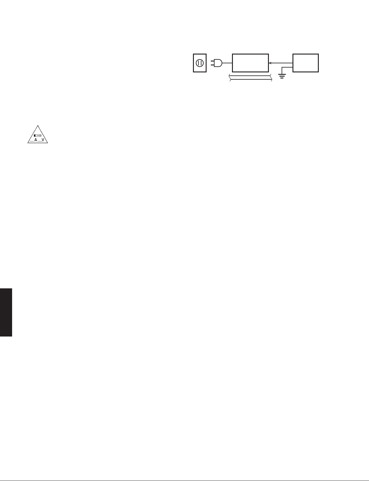
2. Leakage Current Measurement (For 120V Models Only)
When service has been completed, it is imperative to verify
that all exposed conductive surfaces are properly insulated
from supply circuits.
• Meter impedance should be equivalent to 1500 ohms shunted
by 0.15 F.
For U model
“CAUTION”
“F3702: FOR CONTINUED PROTECTION AGAINST RISK OF FIRE, REPLACE ONLY WITH SAME TYPE 8A,
125V FUSE.”
For C model
CAUTION
F3702: REPLACE WITH SAME TYPE 8A, 125V FUSE.
ATTENTION
F3702: UTILISER UN FUSIBLE DE RECHANGE DE MÉME TYPE DE 8A, 125V.
WALL
OUTLET
• Leakage current must not exceed 0.5mA.
• Be sure to test for leakage with the AC plug in both polarities.
EQUIPMENT
UNDER TEST
INSULATING
TABLE
AC LEAKAGE
TESTER OR
EQUIVALENT
WARNING: CHEMICAL CONTENT NOTICE!
This product contains chemicals known to the State of California to cause cancer, or birth defects or other reproductive
harm.
DO NOT PLACE SOLDER, ELECTRICAL/ELECTRONIC OR PLASTIC COMPONENTS IN YOUR MOUTH FOR ANY REASON
WHATSOEVER!
Avoid prolonged, unprotected contact between solder and your skin! When soldering, do not inhale solder fumes or
expose eyes to solder/flux vapor!
If you come in contact with solder or components located inside the enclosure of this product, wash your hands before
handling food.
RX-A720
About lead free solder
RX-V673/HTR-6065/
All of the P.C.B.s installed in this unit and solder joints are soldered using the lead free solder.
Among some types of lead free solder currently available, it is recommended to use one of the following types for the
repair work.
• Sn + Ag + Cu (tin + silver + copper)
• Sn + Cu (tin + copper)
• Sn + Zn + Bi (tin + zinc + bismuth)
Caution:
As the melting point temperature of the lead free solder is about 30°C to 40°C (50°F to 70°F) higher than that of the lead
solder, be sure to use a soldering iron suitable to each solder.
2
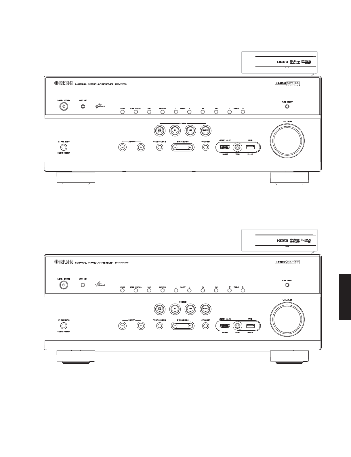
■ FRONT PANELS
RX-V673 (U, C, R, T, K, A, B, G, F, L, S, H models)
RX-V673/HTR-6065/RX-A720
HTR-6065 (A, F models)
RX-V673/HTR-6065/
RX-A720
3
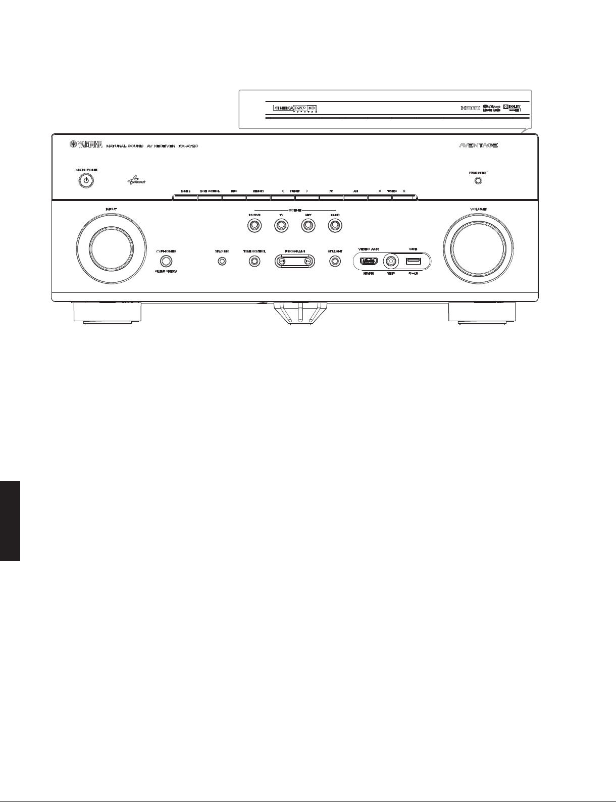
RX-V673/HTR-6065/RX-A720
RX-A720 (U, C, A models)
RX-A720
RX-V673/HTR-6065/
4
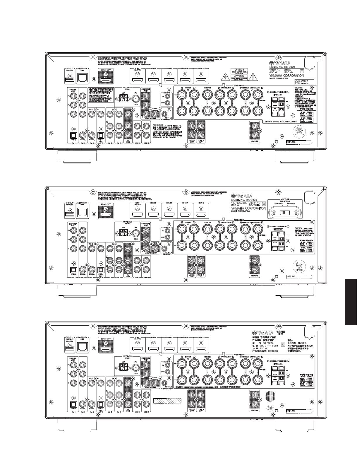
■ REAR PANELS
RX-V673 (U, C models)
RX-V673 (R, S models)
RX-V673/HTR-6065/RX-A720
RX-V673 (T model)
RX-V673/HTR-6065/
RX-A720
5
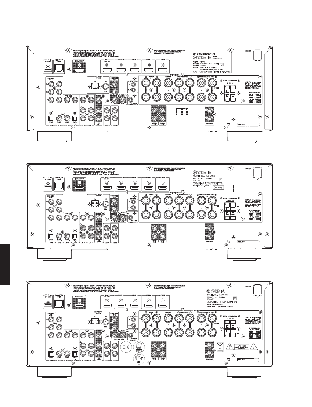
RX-V673/HTR-6065/RX-A720
RX-V673 (K model)
RX-V673 (A model)
RX-A720
RX-V673/HTR-6065/
RX-V673 (B, G, F models)
6
RX-V673 (L, H models)
HTR-6065 (A model)
RX-V673/HTR-6065/RX-A720
H model
HTR-6065 (F model)
RX-V673/HTR-6065/
RX-A720
7
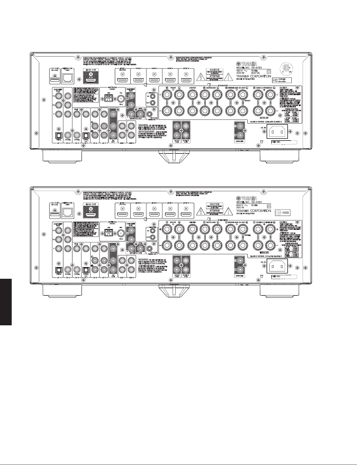
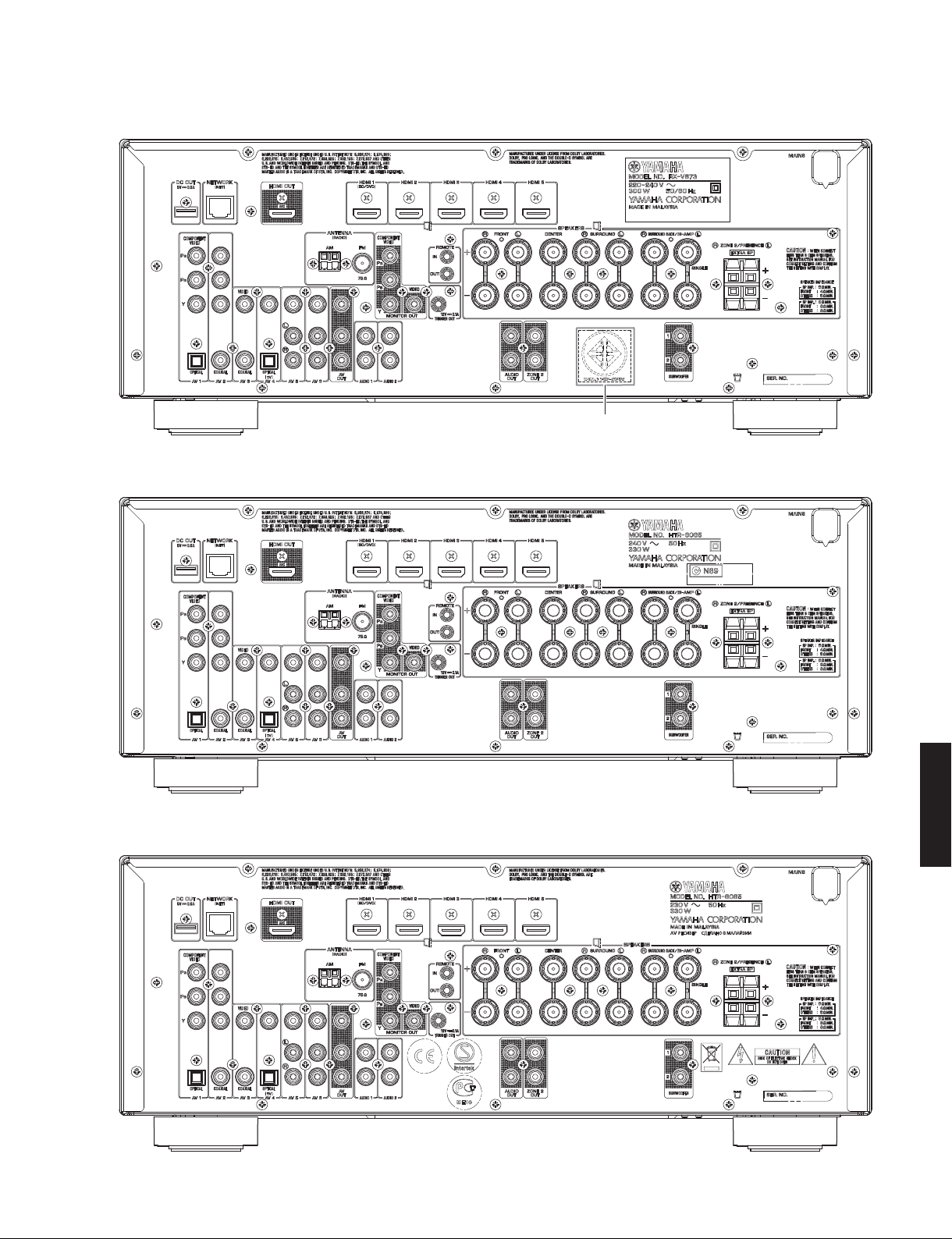
RX-V673/HTR-6065/RX-A720
RX-A720 (U, C models)
RX-A720 (A model)
RX-A720
RX-V673/HTR-6065/
8
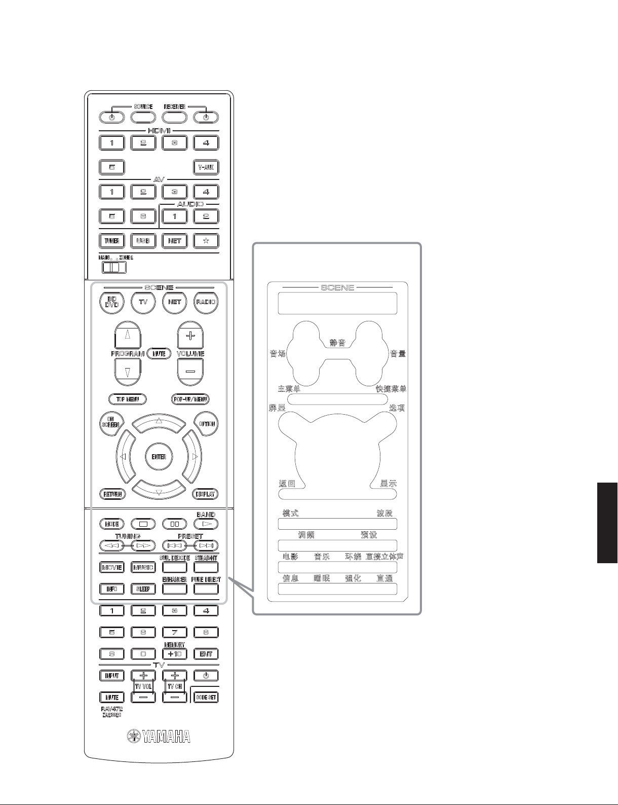
■ REMOTE CONTROL PANEL
RAV472
RX-V673/HTR-6065/RX-A720
Remote control sheet
(T model)
RX-V673/HTR-6065/
RX-A720
9

RX-V673/HTR-6065/RX-A720
■ SPECIFICATIONS
■ Audio Section
Rated Output Power (Power Amp. Section)
(1 kHz, 0.9 % THD)
– 1 channel driven –
U, C, R, T, K, A, B, G, F, L, S, H models (8 ohms)
FRONT L/R ................................................................ 125 W/ch
CENTER .......................................................................... 125 W
SURROUND L/R ........................................................ 125 W/ch
SURROUND BACK L/R .............................................125 W/ch
B, G, F models (4 ohms)
FRONT L/R ................................................................ 150 W/ch
– 2 channels driven simultaneously –
U, C, R, T, K, A, B, G, F, L, S, H models (8 ohms)
FRONT L/R .......................................................105 W + 105 W
CENTER .......................................................................... 105 W
SURROUND L/R ...............................................105 W + 105 W
SURROUND BACK L/R ....................................105 W + 105 W
(20 Hz to 20 kHz, 0.09 % THD)
– 2 channels driven simultaneously –
U, C, R, T, K, A, B, G, F, L, S, H models (8 ohms)
FRONT L/R ...........................................................90 W + 90 W
Maximum Effective Output Power (JEITA) [R, T, K, L, S, H models]
(1 channel driven, 1 kHz, 10 % THD, 8 ohms)
FRONT L/R ......................................................................... 150 W/ch
CENTER .................................................................................. 150 W
SURROUND L/R ................................................................150 W/ch
SURROUND BACK L/R .....................................................150 W/ch
Dynamic Power Per Channel (IHF)
FRONT L/R (1 channel driven)
(8 / 6 / 4 / 2 ohms) ..................................... 130 / 170 / 200 / 240 W
Damping Factor (20 Hz to 20 kHz, 8 ohms)
FRONT L/R to SPEAKER-A ............................................100 or more
Input Sensitivity/Input Impedance (1 kHz, 100 W/8 ohms)
AV5 etc. ............................................................200 mV / 47 k-ohms
Maximum Input Signal (1 kHz, 0.5 % THD)
AV5 etc. (EFFECT ON) .............................................................. 2.3 V
Output Level/Output Impedance
AUDIO OUT ..................................................... 200 mV / 1.2 k-ohms
RX-A720
RX-V673/HTR-6065/
SUBWOOFER (2 ch stereo and FRONT SP: small)
.............................................................................. 1 V / 1.2 k-ohms
ZONE2 OUT ..................................................... 200 mV / 1.2 k-ohms
Headphone Jack Rated Output/Output Impedance
(1 kHz, 50 mV, 8 ohms)
AV5 etc. input .....................................................100 mV / 560 ohms
Frequency Response (10 Hz to 100 kHz)
AV5 etc., FRONT ..................................................................0 / -3 dB
Total Harmonic Distortion (20 Hz to 20 kHz, 50 W/8 ohms)
AV5 etc. (PURE DIRECT) to FRONT SP OUT .............0.06 % or less
Signal to Noise Ratio (IHF-A Network) (Input shorted 250 mV)
AV5 etc. (PURE DIRECT) to SP OUT ....................... 100 dB or more
Residual Noise (IHF-A Network)
FRONT L/R to SP OUT ................................................150 V or less
Channel Separation (1 kHz / 10 kHz)
AV5 etc. (Input 5.1 k-ohms shorted)
...................................................... 60 dB or more / 45 dB or more
Volume Control/Step
......................................... MUTE / -80 dB to +16.5 dB / 0.5 dB step
Tone Control Characteristics
Bass
Boost/Cut ........................................ ±6 dB / 0.5 dB step, at 50 Hz
Turnover frequency .............................................................350 Hz
Treble
Boost/Cut .......................................±6 dB / 0.5 dB step, at 20 kHz
Turnover frequency ............................................................ 3.5 kHz
Filter Characteristics
FRONT, CENTER, SURROUND, SURROUND BACK small (H.P.F.)
....................fc=40/60/80/90/100/110/120/160/200 Hz, 12 dB/oct.
SUBWOOFER small (L.P.F.)
....................fc=40/60/80/90/100/110/120/160/200 Hz, 24 dB/oct.
Optical Jack, Coaxial Jack Support Frequencies
............................................................................... 32 kHz to 96 kHz
■ Video Section
Video Signal Type
Monitor out (Wall paper)
U, C, R, K models .................................................................NTSC
T, A, B, G, F, L, S, H models ..................................................... PAL
Video conversion
.......................................................................................NTSC/PAL
Composite Video Signal Level
...............................................................................1 Vp-p / 75 ohms
Component Video Signal Level
Y .............................................................................1 Vp-p / 75 ohms
Pb/Pr ...................................................................0.7 Vp-p / 75 ohms
Video Maximum Input Level (VIDEO Conversion Off)
................................................................................ 1.5 Vp-p or more
Video Signal to Noise Ratio
................................................................................... 50 dB or more
Monitor Out Frequency Response (VIDEO Conversion Off)
Component video signal level .......................5 Hz to 60 MHz, -3 dB
■ FM Section
Tuning Range
U, C models ......................................................... 87.5 to 107.9 MHz
R, L, S, H models ..................... 87.5 to 108.0 / 87.50 to 108.00 MHz
T, K, A, B, G, F models ....................................87.50 to 108.00 MHz
50 dB Quieting Sensitivity (IHF) (1 kHz, 100 % MOD.)
Mono ......................................................................... 3 µV (20.8 dBf)
Signal to Noise Ratio (IHF)
Mono ........................................................................................71 dB
Stereo ......................................................................................69 dB
Harmonic Distortion (1 kHz)
Mono ........................................................................................ 0.3 %
Stereo ......................................................................................0.5 %
Antenna Input
......................................................................... 75 ohms unbalanced
10

■ AM Section
Tuning Range
U, C models ........................................................... 530 to 1,710 kHz
R, L, S, H models ............................ 530 to 1,710 / 531 to 1,611 kHz
T, K, A, B, G, F models ..........................................531 to 1,611 kHz
Antenna
..................................................................................... Loop antenna
■ General
Power Supply
U, C models ............................................................ AC 120 V, 60 Hz
R, S models .................................AC 110–120/220–240 V, 50/60 Hz
T model ................................................................... AC 220 V, 50 Hz
K model .................................................................. AC 220 V, 60 Hz
A model .................................................................. AC 240 V, 50 Hz
B, G, F models ........................................................ AC 230 V, 50 Hz
L, H models ............................................... AC 220–240 V, 50/60 Hz
Power Consumption
U, C models ..............................................................400 W / 500 VA
R, L, S, H models .................................................................... 300 W
T, K, A, B, G, F models ...........................................................330 W
Standby Power Consumption (reference data)
HDMI control: OFF / Standby through: OFF
................................................................................ 0.1 W (typical)
HDMI control: ON / Standby through: ON
INPUT: HDMI1(HDMI no signal)
.............................................................................3.0 W (typical)
Network standby: ON
................................................................................ 2.0 W (typical)
Maximum Power Consumption [R, L, S, H models]
................................................................................................ 590 W
Dimensions (W x H x D)
[RX-V673/HTR-6065]
............................ 435 x 171 x 364 mm (17-1/8" x 6-3/4" x 14-3/8")
[RX-A720]
............................ 435 x 171 x 367 mm (17-1/8" x 6-3/4" x 14-1/2")
Weight
[RX-V673/HTR-6065]
........................................................................... 10.2 kg (22.5 lbs.)
[RX-A720]
........................................................................... 10.7 kg (23.6 lbs.)
Finish
[RX-V673]
T model ..........................................................................Gold color
U, C, R, T, K, A, B, G, F, L, S, H models ....................... Black color
R, B, G, F, L, H models .............................................Titanium color
[HTR-6065]
A, F models .................................................................. Black color
[RX-A720]
U, C, A models ............................................................. Black color
RX-V673/HTR-6065/RX-A720
Accessories
Remote control ..............................................................................x 1
Batteries (R03, AAA, UM-4) ..........................................................x 2
FM antenna (1.4 m) ......................................................................x 1
AM antenna (1.0 m) ......................................................................x 1
YPAO microphone (6.0 m) ............................................................x 1
Remote control sheet (T model) ...................................................x 1
Power cable (2.0 m) (RX-A720) ....................................................x 1
* Specifications are subject to change without notice.
U ........................U.S .A. model
C ..................Canadian model
R .....................General model
T..................... Chinese model
K ...................... Korean model
A .................Australian model
Manufactured under license from Dolby Laboratories. Dolby, Pro Logic and
the double-D symbol are trademarks of Dolby Laboratories.
DTS-HD, the Symbol, & DTS-HD and the Symbol together are registered
trademarks & DTS-HD Master Audio is a trademark of DTS, Inc.
Product includes software. © DTS, Inc. All Rights Reserved.
AirPlay, the AirPlay logo, iPad, iPhone, iPod, iPod nano, and iPod touch are
trademarks of Apple Inc., registered in the U.S. and other countries.
MPEG Layer-3 audio coding technology licensed from Fraunhofer IIS and
Thomson.
This receiver supports network connections.
“HDMI,” the “HDMI” logo and “High-Definition Multimedia Interface” are
trademarks, or registered trademarks of HDMI Licensing LLC.
“x.v.Color” is a trademark of Sony Corporation.
B .......................British model
G ..................European model
F..................... Russian model
L..................Singapore model
S ...................Brazirian model
H ...........................Thai model
RX-V673/HTR-6065/
RX-A720
11
RX-V673/HTR-6065/RX-A720
“SILENT CINEMA” is a trademark of Yamaha Corporation.
DLNA™ and DLNA CERTIFIED™ are trademarks or registered trademarks
of Digital Living Network Alliance. All rights reserved. Unauthorized use is
strictly prohibited.
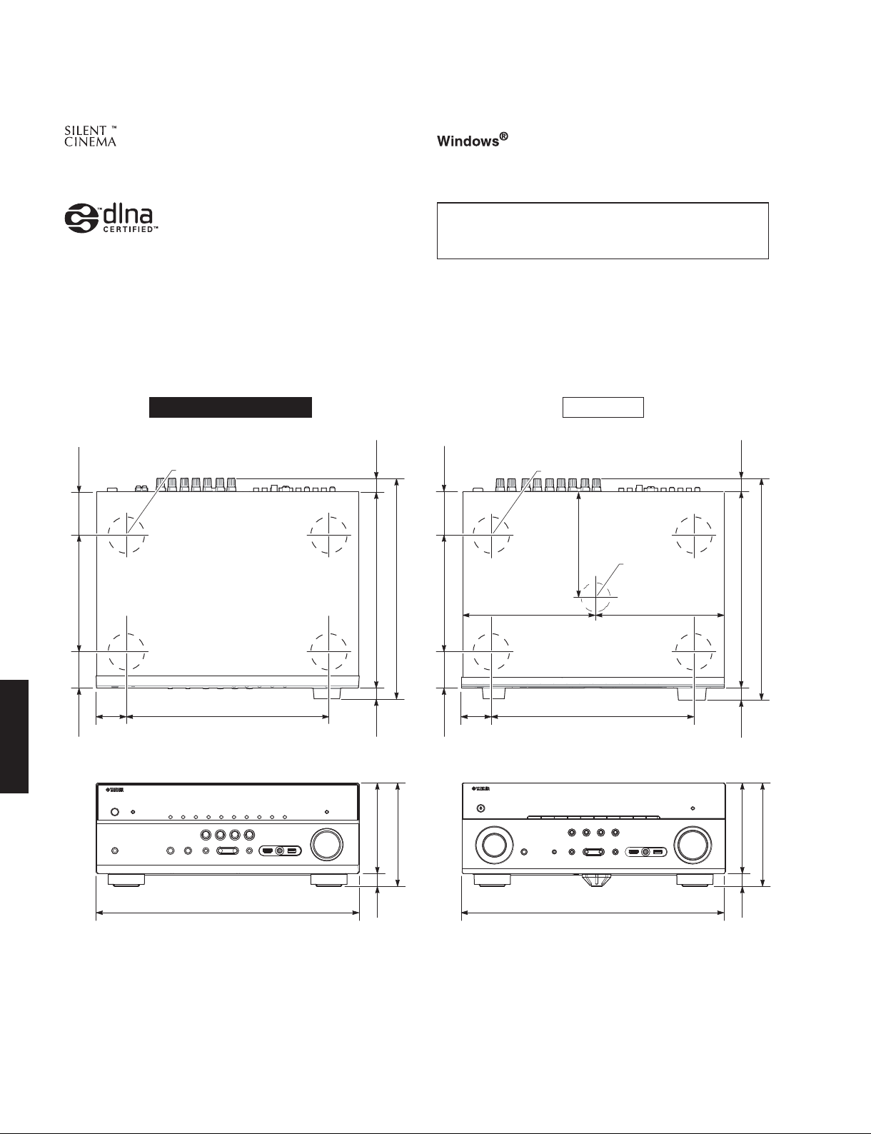
• DIMENSIONS
RX-V673/HTR-6065 RX-A720
72
Top view
(2-7/8")
ø 60
22
(7/8")
Windows is a registered trademark of Microsoft Corporation in the United
States and other countries.
Windows XP, Windows Vista, Windows 7, Windows Media Audio, Windows
Media Connect and Windows Media Player are either registered trademarks
or trademarks of Microsoft Corporation in the United States and/or other
countries.
72
Top view
(2-7/8")
ø 60
173 (6-3/4")
ø 48/18
22
(7/8")
193 (7-5/8")
59
(2")
(2-1/4")
RX-A720
Front view
RX-V673/HTR-6065/
50
335 (13-1/4")
435 (17-1/8")
364 (14-3/8")
324 (12-3/4")
18
(3/4")
150 (5-7/8")
171 (6-3/4")
21
(7/8")
193 (7-5/8")
50
59
(2")
(2-1/4")
Front view
222.5 (8-3/4") 212.5 (8-3/8")
335 (13-1/4")
435 (17-1/8")
Unit: mm (inch)Unit: mm (inch)
367 (14-1/2")
324 (12-3/4")
21
(7/8")
150 (5-7/8")
171 (6-3/4")
21
(7/8")
12
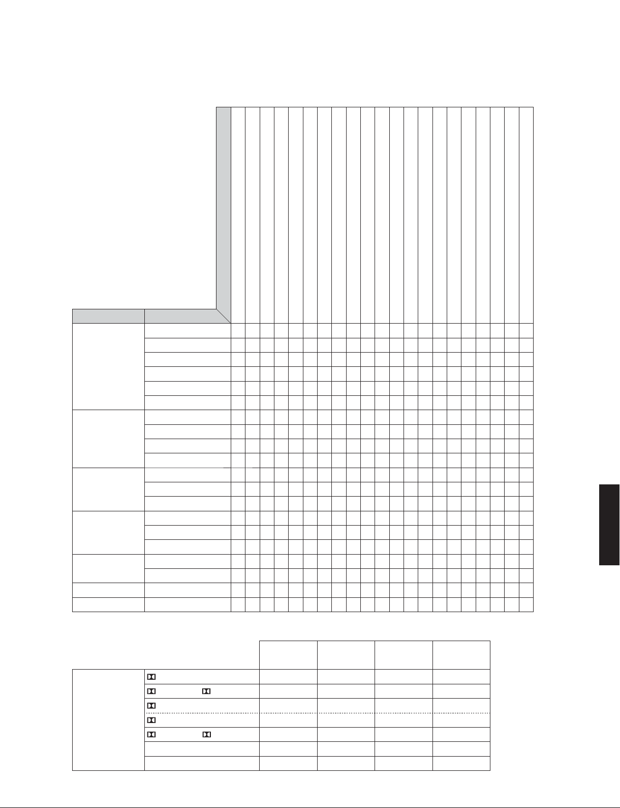
• SELECT MENU
Sound field parameters
RX-V673/HTR-6065/RX-A720
Parameter
Category Program
MOVIE THEATER Standard
Spectacle
Sci-Fi
Adventure
Drama
Mono Movie
ENTERTAINMENT Sports
Action Game
Roleplaying Game
Music Video
CLASSICAL Hall in Munich
Hall in Vienna
Chamber
LIVE/CLUB Cellar Club
The Roxy Theatre
The Bottom Line
STEREO 2ch Stereo
7ch Stereo
SUR. DECODE SURROUND DECODER
STRAIGHT
Decode Type (*1)
DSP Level: -6 to +3 dB, [0]
Initial Delay: 1 to 99 ms
Surround Initial Delay: 1 to 49 ms
Surround Back Initial Delay: 1 to 49 ms
Room Size: 0.1 to 2.0
Surround Room Size: 0.1 to 2.0
Surround Back Room Size: 0.1 to 2.0
Liveness: 0 to 10
Surround Liveness: 0 to 10
Surround Back Liveness: 0 to 10
Reverb Time: 1.0 to 5.0 s
Reverb Delay: 0 to 250 ms
Reverb Level: 0 to 100 %
Direct: Auto / Off, [Auto]
Level: -5 to +5, [0]
Front/Rear Balance: -5 to +5, [0]
Left/Right Balance: -5 to +5, [0]
Height Balance: 0 to 10, [5]
Monaural Mix: Off / On, [Off]
Reset
●● ●○ ●○ ●○ ●
●●●●○●●○ ●
●●●●○●●○ ●
●●●●○●●○ ●
●●●●○●●○ ●
●● ● ● ●●● ●
●●●○●●○ ●
●●●○●●○ ●
●●●○●●○ ●
●●●○●●○ ●
●● ● ● ●
●● ● ● ●
●● ● ●●● ●
●● ● ● ●
●● ● ● ●●● ●
●● ● ● ●
●●
●●●●●●
● ●
RX-V673/HTR-6065/
RX-A720
*1 Surround Decoder
Decode Type
Pro Logic
PL IIx Movie / PL II Movie
PL IIx Music /
PL II Music
PL IIx Game / PL II Game
Neo:6 Cinema
Neo:6 Music
Panorama Center Width Dimension Center Image
Off / On, [Off] 0 to 7, [3] -3 to +3, [0] 0.0 to 1.0, [0.3]
●●●
●
13
RX-V673/HTR-6065/RX-A720
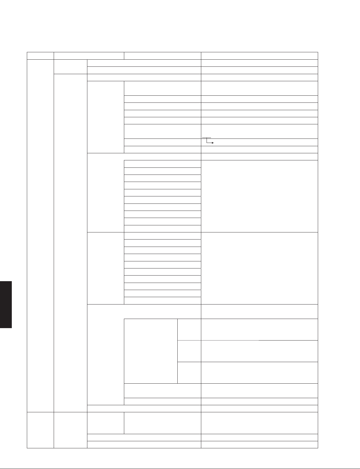
• SET MENU TABLE
MAIN MENU SUB-MENU PARAMETER VALUE [INITIAL VALUE]
Speaker Auto Measure Optimizes the speaker configuration automatically using YPAO.
Setup Result Not Available
Manual Power Amp Assign [Basic] / 7ch +1ZONE / 5ch BI-AMP
RX-A720
RX-V673/HTR-6065/
Sound Setup Lipsync Delay Enable HDMI1 / HDMI2 / HDMI3 / HDMI4 /
Configuration Front Large / [Small]
* When “Subwoofer” is set to “None”, “Front” is disabled.
Center Large / [Small] / None
Surround Large / [Small] / None
Surround Back Large x1 / Large x2 / Small x1 / [Small x2] / None
Front Presence [Use] / None
Subwoofer [Use] / None
[Normal] / Reverse
Extra Bass Not Available
Bass Cross Over 40 / 60 / [80] / 90 / 100 / 110 / 120 / 160 / 200 Hz
Distance Meter / Feet
Front L
Front R
Center
Surround L
Surround R 0.30 to 24.00 m, [3.00 m], 0.05 m step
Surround Back L 1.0 to 80.0 ft, [10.0 ft], 0.2 ft step
Surround Back R
Front Presence L
Front Presence R
Subwoofer
Level Front L
Front R
Center
Surround L
Surround R -10.0 to +10.0 dB, [0.0 dB], 0.5 dB step
Surround Back L
Surround Back R
Front Presence L
Front Presence R
Subwoofer
Parametric EQ Manual / YPAO : Flat / YPAO : Front / YPAO : Natural / [Through]
* Select “ENTER”
Front L Band
Front R / Gain▲ Gain: -20.0 to +6.0 dB, [0.0 dB], 0.5 dB step
Center
Surround L Frequency▶ Frequency: 31.3 Hz to 16.0 kHz, [62.5 Hz]
Surround R / Gain▲ Gain: -20.0 to +6.0 dB, [0.0 dB], 0.5 dB step
Surround Back L
Surround Back R Q
Front Presence L / Gain▲ Gain: -20.0 to +6.0 dB, [0.0 dB], 0.5 dB step
Front Presence R
PEQ Data Copy Flat > Manual / Front > Manual / Natural > Manual
PEQ Data Clear OK / CANCEL * Select “ENTER”
Test Tone [Off] / On
HDMI5 / AV1 / AV2 / AV3 / AV4 / AV5 / Disable / [Enable]
AV6 / AUDIO1 / AUDIO2
Auto/Manual Select [Auto] / Manual
Adjustment 0 to 500 ms, [0 ms], 1 ms step
Band: #1 to #7
▶
Q: 0.500 to 10.080, [1.000]
▶
* Select “ENTER”
14
RX-V673/HTR-6065/RX-A720
MAIN MENU SUB-MENU PARAMETER VALUE [INITIAL VALUE]
Sound Setup Dynamic Range [Maximum] / Standard / Minimum/Auto
Max. Volume -30.0 to +16.5 dB (Maximum volume), [+16.5 dB], 5.0 dB step
Initial Volume [Off] / On
Select “On” Mute, -80 to +16.5 dB, 0.5 dB step
Adaptive DSP Level Off / [On]
Video Setup Video Mode [Direct] / Processing
Select Resolution Through / [Auto] / 576p / 720p / 1080i / 1080p / 4K
“Processing” * Select “ENTER”
Aspect [Through] / 16:9 Normal
HDMI Setup HDMI Control [Off] / On
TV Audio Input AV1 / AV2 / AV3 / [AV4] / AV5 / AV6 / AUDIO1 / AUDIO2
ARC (Audio Return Channel) Off / [On]
Standby Sync Off / On / [Auto]
Audio Output Amp Off / [On]
HDMI OUT (TV) [Off] / On
Standby Through [Off] / On
* When HDMI Control is set to “On”, “Standby Through” is
disabled.
Network IP Address DHCP [Off] / On
Setup IP Address xxx.xxx.xxx. x
Subnet Mask xxx.xxx.xxx. x
Default Gateway xxx.xxx.xxx. x
DNS Server (P) Primary x. x. x. x
DNS Server (S) Secondary x. x. x. x
Network Standby [Off] / On
MAC Address Filter [Off] / On
Filter MAC Address 1–5 xx : xx : xx : xx : xx : xx
6–10
Network Name Input is possible to 15 characters
Multi Zone Main Zone Set Zone Rename Input is possible to 9 characters
Setup Zone2 Set Max. Volume -30.0 to +16.5 dB (Maximum volume), [+16.5 dB], 5.0dB step
Initial Volume [Off] / On
Select “On” Mute, -80 to +16.5 dB, 0.5 dB step
Zone Rename Input is possible to 9 characters
Function Display Set Dimmer (Front Display) -4 to 0
Setup Short Message [On] / Off
Wall Paper Picture1 / Picture2 / Picture3 / Gray
Trigger Output Trigger Mode [Power] / Source / Manual
Select “Source” HDMI1–5, AV1–6, V-AUX, AUDIO1–2, TUNER, AirPlay,
SERVER, NET RADIO, USB
Low / [High]
Target Zone Main / Zone2 / [All]
Memory Guard [Off] / On
ECO Setup Auto Power Down Off / 2 Hours / 4 Hours / 8 Hours / 12 Hours
U, C, R, T, K, A, L, S, H models: [Off]
B, G, F models: [8 Hours]
ECO Mode [Off] / On
Language [English (English)] /
Setup Deutsch (German) / Español (Spanish) / Рyccкий (Russian) /
(Chinese)
中文
(Japanese) / Français (French) /
日本語
RX-V673/HTR-6065/
RX-A720
15
RX-V673/HTR-6065/RX-A720
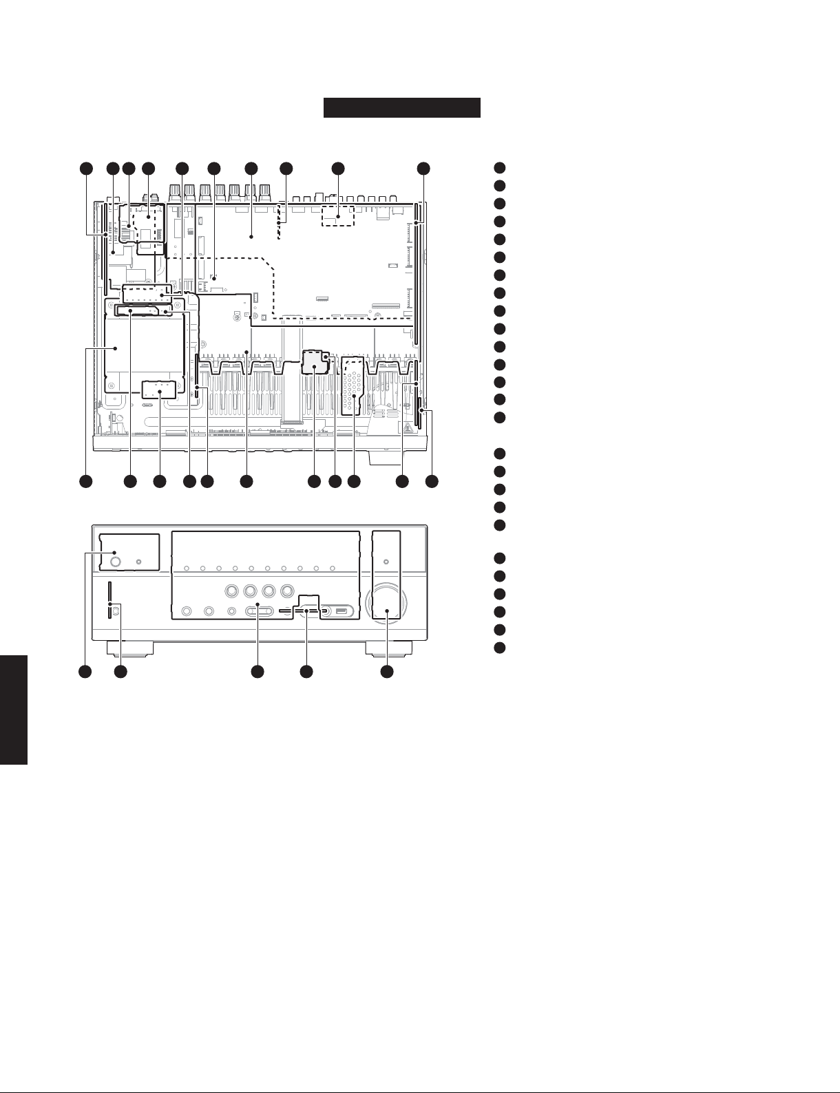
■ INTERNAL VIEW
RX-V673/HTR-6065
Top view
18
523 4 6 7 9
1516 131920
Front view
10
111421 1218 17
1
VIDEO (2) P.C.B.
2
VIDEO (3) P.C.B.
3
VIDEO (8) P.C.B. (R, S models)
4
OPERATION (8) P.C.B.
5
MAIN (2) P.C.B.
6
DIGITAL (1) P.C.B.
7
VIDEO (1) P.C.B.
8
VIDEO (4) P.C.B.
9
AM/FM TUNER
10
OPERATION (2) P.C.B.
11
OPERATION (12) P.C.B.
12
OPERATION (7) P.C.B.
13
OPERATION (11) P.C.B.
14
OPERATION (9) P.C.B. (U, C models)
15
OPERATION (10) P.C.B.
(R, T, K, A, B, G, F, L, S, H models)
6
MAIN (1) P.C.B.
16
MAIN (6) P.C.B.
17
VIDEO (9) P.C.B. (R, S models)
18
VIDEO (7) P.C.B.
19
VIDEO (6) P.C.B.
20
(U, C, T, K, A, B, G, F, L, H models)
POWER TRANSFORMER
21
OPERATION (4) P.C.B.
22
OPERATION (3) P.C.B.
23
OPERATION (1) P.C.B.
24
DIGITAL (2) P.C.B.
25
OPERATION (5) P.C.B.
26
22 23 24 25 26
RX-A720
RX-V673/HTR-6065/
16
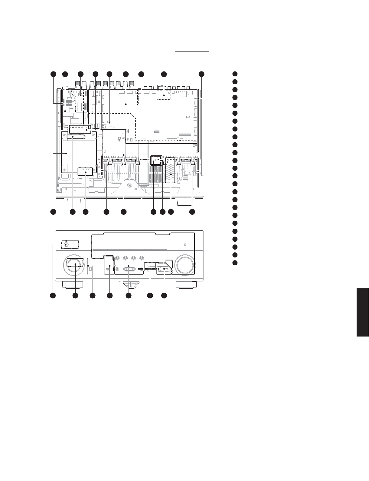
RX-A720
Top view
17
423 5 6 8
1218 1015
1314 111617
9
Front view
1
2
3
4
5
6
7
8
9
10
11
12
13
14
15
16
17
18
19
20
21
22
23
24
25
RX-V673/HTR-6065/RX-A720
VIDEO (2) P.C.B.
VIDEO (3) P.C.B.
OPERATION (8) P.C.B.
MAIN (2) P.C.B.
DIGITAL (1) P.C.B.
VIDEO (1) P.C.B.
VIDEO (4) P.C.B.
AM/FM TUNER
OPERATION (2) P.C.B.
OPERATION (7) P.C.B.
OPERATION (11) P.C.B.
OPERATION (9) P.C.B. (U, C models)
OPERATION (10) P.C.B. (A model)
MAIN (1) P.C.B.
MAIN (6) P.C.B.
VIDEO (7) P.C.B.
VIDEO (6) P.C.B.
POWER TRANSFORMER
OPERATION (5) P.C.B.
OPERATION (6) P.C.B.
OPERATION (3) P.C.B.
OPERATION (4) P.C.B.
OPERATION (1) P.C.B.
DIGITAL (2) P.C.B.
OPERATION (12) P.C.B.
19 21 232220 24 25
■ SERVICE PRECAUTIONS
Safety measures
• Some internal parts in this product contain high voltages and are dangerous.
Be sure to take safety measures during servicing, such as wearing insulating gloves.
• Note that the capacitors indicated below are dangerous even after the power is turned off because an electric charge
remains and a high voltage continues to exist there.
Before starting any repair work, connect a discharging resistor (5 k-ohms/10 W) to the terminals of each capacitor
indicated below to discharge electricity.
The time required for discharging is about 30 seconds per each.
C1082–C1085 on MAIN P.C.B.
C3706 on VIDEO (2) P.C.B.
For details, refer to “PRINTED CIRCUIT BOARDS”.
RX-V673/HTR-6065/
RX-A720
17
RX-V673/HTR-6065/RX-A720
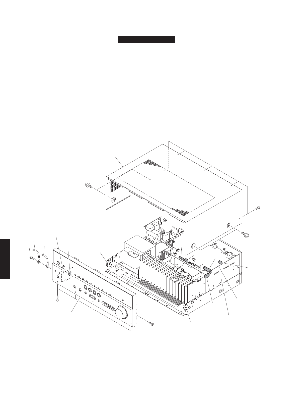
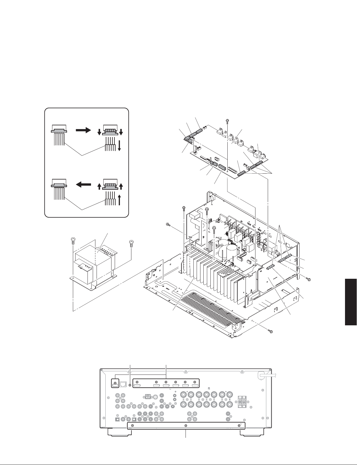
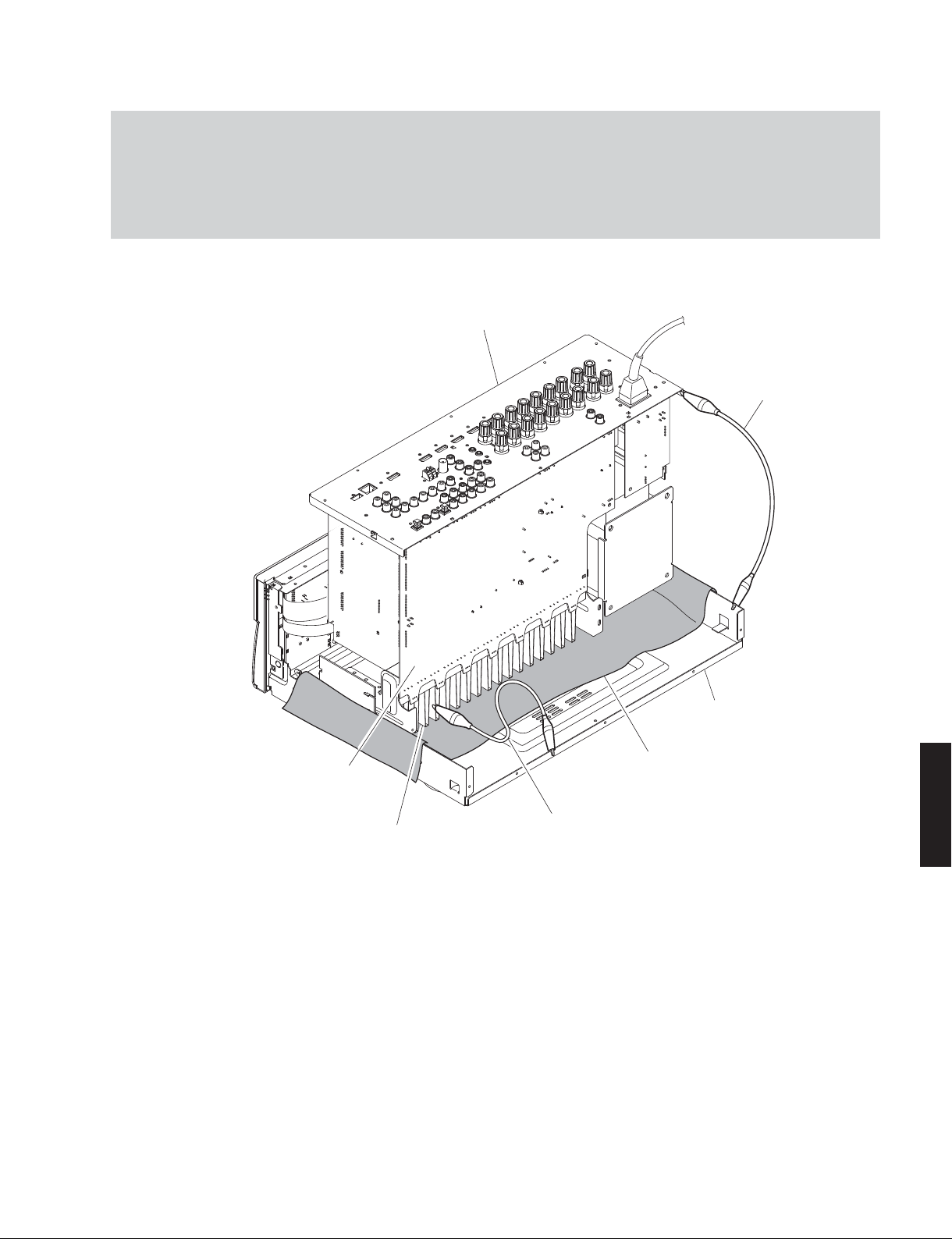
■ DISASSEMBLY PROCEDURES
RX-V673/HTR-6065
(Remove parts in the order as numbered.)
Disconnect the power cable from the AC outlet.
1. Removal of Top Cover
a. Remove 4 screws (①) and 5 screws (②). (Fig. 1)
b. Lift the rear of the top cover to remove it. (Fig. 1)
2. Removal of Front Panel Unit
a. Remove 6 screws (③), and remove W4401 and W4421. (Fig. 1)
b. Remove CB8, CB82, CB458, CB472, CB947 and CB952. (Fig. 1)
c. Release 2 hooks, and remove the front panel unit. (Fig. 1)
Top cover
W4401
RX-A720
RX-V673/HTR-6065/
③
OPERATION (3) P.C.B.
W4421
CB472
③
Front panel unit
①
Hook
③
CB8
Hook
CB947
②
①
CB82
CB952
DIGITAL (1) P.C.B.
CB458
OPERATION (2) P.C.B.
18
Fig. 1
RX-V673/HTR-6065/RX-A720
3. Removal of DIGITAL (1) P.C.B.
a. Remove screw (④) and 7 screws (⑤). (Fig. 3)
b. Remove 3 screws. (⑥). (Fig. 2)
c. Remove CB21, CB76, CB81 and CB942. (Fig. 2)
d. Unlock and remove CB78, CB79 and CB944. (Fig. 2)
e. Remove the DIGITAL (1) P.C.B. which is connected
directly to the OPERATION (2) P.C.B. with board-toboard connectors. (Fig. 2)
Remove CB78, CB79 and CB944
Connected
Cable
Connect CB78, CB79 and CB944
Connected
Cable
Unlock the connector
①
Remove the cable
②
①①
②
Lock the connector
①
Insert the cable
②
①①
②
CB942
CB944
⑦
⑩
Power transformer
⑩
4. Removal of AMP Unit and Power Transformer
a. Remove screw (⑦), 3 screws (⑧), 3 screws (⑨) and
4 screws (⑩). (Fig. 2)
b. Remove 3 screws (⑪). (Fig. 3)
c. Remove the AMP unit together with the power
transformer. (Fig. 2)
CB21
CB76
CB81
CB79
⑥
DIGITAL (1) P.C.B.
CB945
CB946
CB948
Board-to-board connectors
CB78
⑨
⑧
Board-to-board connectors
⑧
AMP unit
⑤④
Fig. 2
Rear view
CB459
CB460
CB461
OPERATION (2) P.C.B.
⑨
⑥
RX-V673/HTR-6065/
RX-A720
⑪
Fig. 3
19
RX-V673/HTR-6065/RX-A720
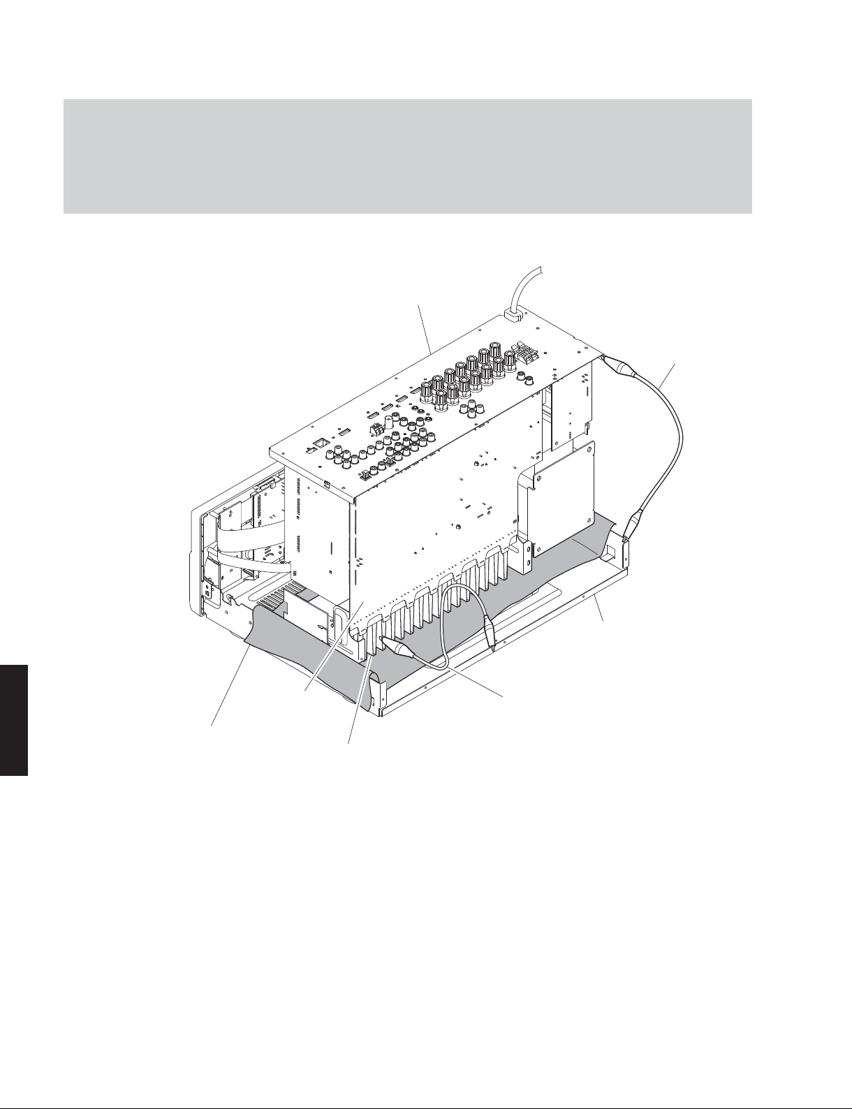
When checking the P.C.B.s:
• Place the P.C.B.s (with rear panel) upright. (Fig. 4)
• Connect the heatsink and rear panel to the chassis with a ground lead. (Fig. 4)
• Reconnect all cables (connectors) that have been disconnected.
• When connecting the flexible flat cable, be careful with polarity.
Rear panel
Ground lead
RX-A720
RX-V673/HTR-6065/
MAIN (1) P.C.B.
Rubber sheet and cloth
Chassis
Ground lead
Heatsink
Fig. 4
20
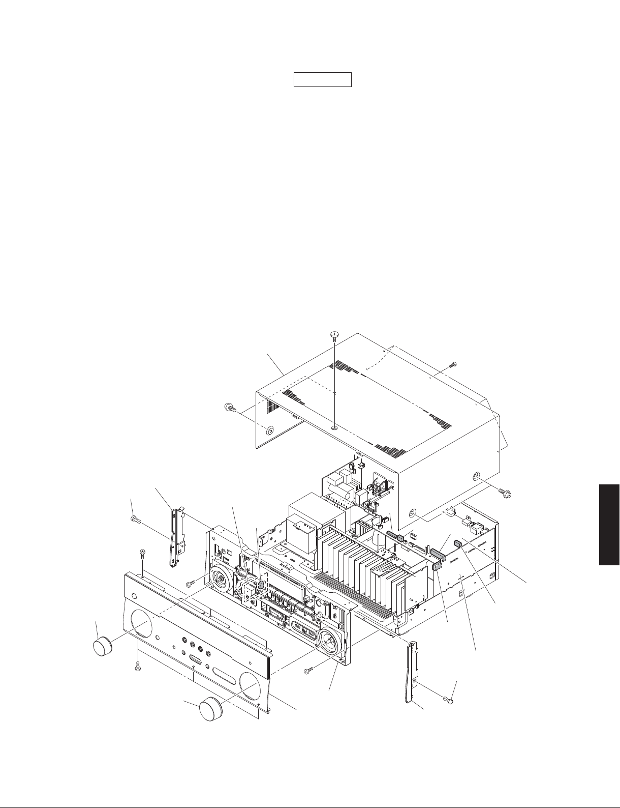
RX-A720
(Remove parts in the order as numbered.)
Disconnect the power cable from the AC outlet.
1. Removal of Top Cover
a. Remove 4 screws (①), 5 screws (②) and screw (③). (Fig. 1)
b. Lift the rear of the top cover to remove it. (Fig. 1)
2. Removal of Front Panel Unit and Sub-Chassis Unit
a. Remove knob (INPUT) and knob (VOLUME). (Fig. 1)
b. Remove 6 screws (④) and then remove the front panel unit. (Fig. 1)
c. Remove 2 push rivets and then remove the side plate (L) and side plate (R). (Fig. 1)
d. Remove CB8, CB82, CB458, CB471, CB947 and CB952. (Fig. 1)
e. Remove 2 screws (⑤) and then remove the sub-chassis unit. (Fig. 1)
RX-V673/HTR-6065/RX-A720
Knob
(INPUT)
Side plate (L)
Push rivet
④
①
OPERATION (3) P.C.B.
⑤
Top cover
CB471
③
CB8
CB947
CB82
CB458
②
①
DIGITAL (1) P.C.B.
CB952
RX-V673/HTR-6065/
RX-A720
④
(VOLUME)
Knob
⑤
Sub-chassis unit
Front panel unit
Fig. 1
OPERATION (2) P.C.B.
Push rivet
Side plate (R)
21
RX-V673/HTR-6065/RX-A720
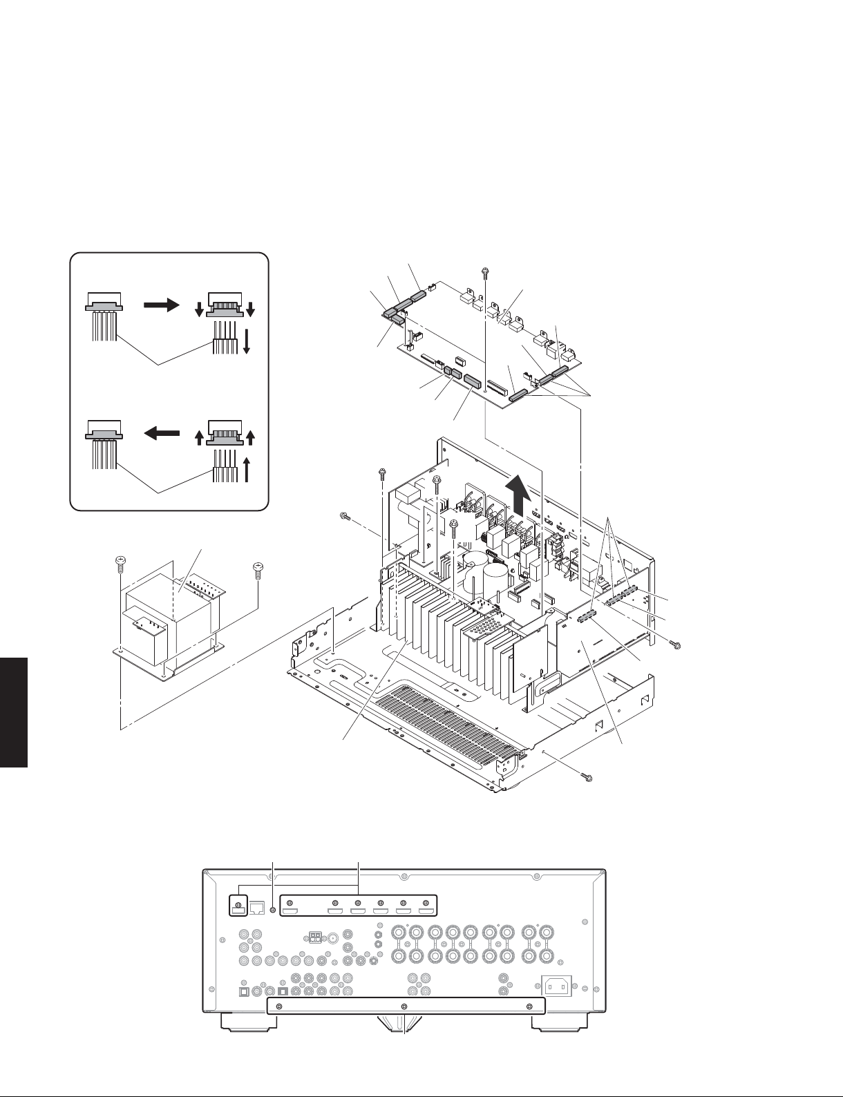
3. Removal of DIGITAL (1) P.C.B.
a. Remove screw (⑥) and 7 screws (⑦). (Fig. 3)
b. Remove 3 screws. (⑧). (Fig. 2)
c. Remove CB21, CB76, CB81 and CB942. (Fig. 2)
d. Unlock and remove CB78, CB79 and CB944. (Fig. 2)
e. Remove the DIGITAL (1) P.C.B. which is connected
directly to the OPERATION (2) P.C.B. with board-toboard connectors. (Fig. 2)
Remove CB78, CB79 and CB944
Connected
Cable
Connect CB78, CB79 and CB944
Connected
Cable
⑫
Unlock the connector
①
Remove the cable
②
①①
Lock the connector
①
Insert the cable
②
①①
Power transformer
②
②
⑨
⑫
CB76
CB942
CB944
⑪
4. Removal of AMP Unit and Power Transformer
a. Remove screw (⑨), 3 screws (⑩), 3 screws (⑪) and
4 screws (⑫). (Fig. 2)
b. Remove 3 screws (⑬). (Fig. 3)
c. Remove the AMP unit together with the power
transformer. (Fig. 2)
CB21
CB81
CB79
CB78
⑧
DIGITAL (1) P.C.B.
CB945
CB946
CB948
Board-to-board connectors
⑩
Board-to-board connectors
⑩
RX-A720
RX-V673/HTR-6065/
AMP unit
CB459
CB460
⑧
CB461
OPERATION (2) P.C.B.
⑪
Fig. 2
⑦⑥
Rear view
22
⑬
Fig. 3
When checking the P.C.B.s:
• Place the P.C.B.s (with rear panel) upright. (Fig. 4)
• Connect the heatsink and rear panel to the chassis with a ground lead. (Fig. 4)
• Reconnect all cables (connectors) that have been disconnected.
• When connecting the flexible flat cable, be careful with polarity.
Rear panel
RX-V673/HTR-6065/RX-A720
Ground lead
MAIN (1) P.C.B.
Heatsink
Fig. 4
Ground lead
Chassis
Rubber sheet and cloth
RX-V673/HTR-6065/
RX-A720
23

RX-V673/HTR-6065/RX-A720
■ UPDATING FIRMWARE
When the following parts are replaced, the firmware must be updated to the latest version.
DIGITAL P.C.B.
FPGA Flash ROM: IC77 on DIGITAL P.C.B.
DSP(TI) Flash ROM: IC923 on DIGITAL P.C.B.
NETWORK Flash ROM: IC953 on DIGITAL P.C.B.
● Confirmation of firmware version and checksum
Before and after updating the firmware, check the firmware version and checksum by using the self-diagnostic
function menu.
Start up the self-diagnostic function and select “S4. ROM VERSION/CHECKSUM” menu.
Using the sub-menu, have the firmware version and checksum displayed, and note them down.
(See “SELF-DIAGNOSTIC FUNCTION”)
* When the firmware version is different from written one after updating, perform the updating procedure again from
the beginning again.
● Initializing the back-up IC (EEPROM: IC82 on DIGITAL P.C.B.)
After updating the firmware, the back-up IC MUST be initialized by the following procedure to store the setting
information (soundfield parameters, system memory and tuner presetting, etc.) properly.
Start up the self-diagnostic function and select “S3. FACTORY PRESET” menu. (See “SELF-DIAGNOSTIC FUNCTION”)
Select “PRESET RSRV”, press the “MAIN ZONE
the back-up IC is initialized.
● Required Tools
• USB storage device
• Firmware
● Preparation
RX-A720
RX-V673/HTR-6065/
1. Download the latest firmware from the specified download source to the folder of the PC.
2. Copy the latest firmware from the PC to the root folder of the USB storage device.
Note) When the latest firmware is copied to a sub-folder of the USB storage device, the update will not proceed.
” key to turn off the power once and turn on the power again. Then
RX-V673/HTR-6065/RX-A720: R0309-xxxx.bin
24
RX-V673/HTR-6065/RX-A720
● Operation Procedures
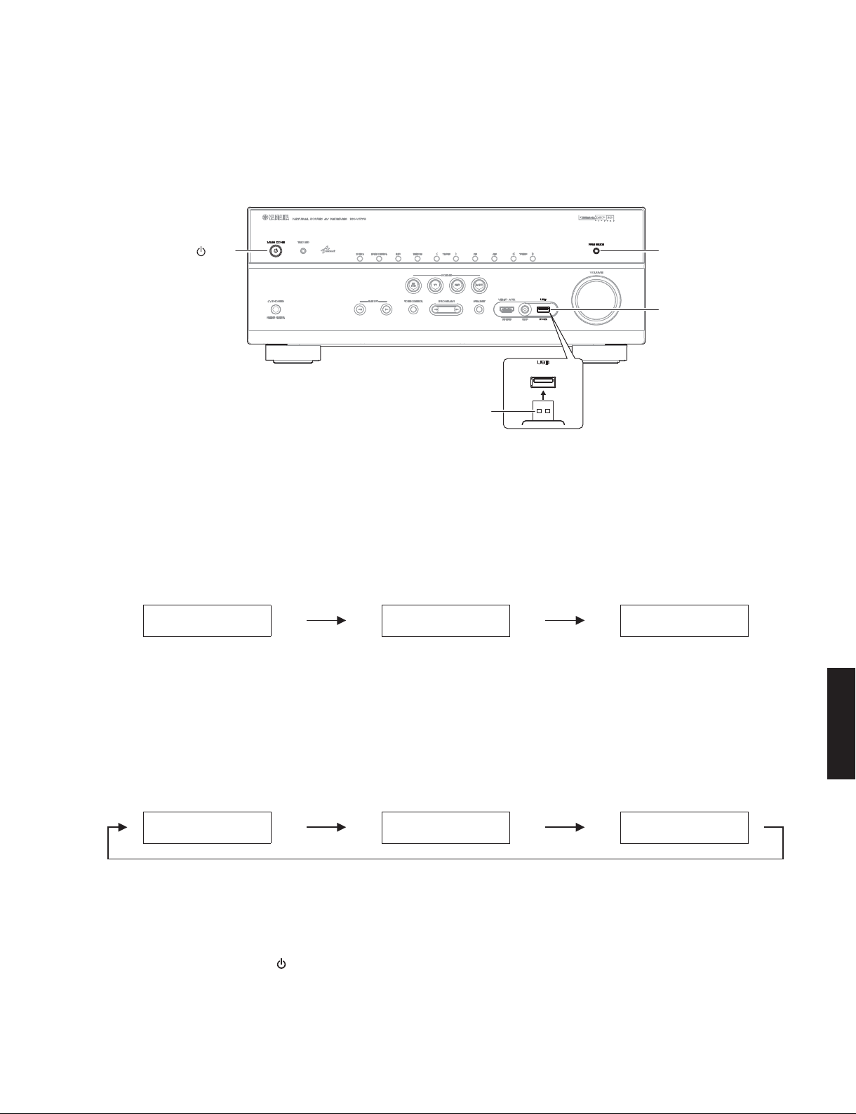
1. Insert the USB storage device to the USB jack. (Fig. 1)
2. While pressing the “PURE DIRECT” key, connect the power cable to the AC outlet. (Fig. 1)
"MAIN ZONE " key "PURE DIRECT" key
USB jack
USB storage device
Fig. 1
3. The USB UPDATE mode is activated and “USB UPDATE” is displayed. Writing of the firmware starts automatically.
(Fig. 2)
Writing is started.
USBUPDATE
VERIFYING...
Writing being executed.
Sx-x:xx%
Fig. 2
4. When writing of the firmware is completed, “UPDATE SUCCESS”, “PLEASE...” and “POWER OFF!” are displayed
repeatedly. (Fig. 3)
Writing is completed.
UPDATESUCCESS
PLEASE...
POWEROFF!
RX-V673/HTR-6065/
RX-A720
Fig. 2
5. Press the “MAIN ZONE
” key to turn off the power. (Fig. 1)
6. Remove the USB storage device from the USB jack. (Fig. 1)
7. Start up the self-diagnostic function and check that the firmware version and checksum are the same as written
ones. (See “Confirmation of firmware version and checksum”)
25
RX-V673/HTR-6065/RX-A720
■ SELF-DIAGNOSTIC FUNCTION
This unit has self-diagnostic functions that are intended for inspection, measurement and location of faulty point.
There are 22 main menu items, each of which has sub-menu items.
Listed in the table below are main menu items and sub-menu items.
Note: Some of the menu items listed below may not apply to the models covered in this service manual.
No. Main menu No. Sub-menu
A: Audio system
A1 DSP AUDIO 1 DSP MARGIN
A2 DIRECT AUDIO 1 ANALOG DIRECT VH
A3 HDMI AUDIO 1 HDMI AUTO
A4 SPEAKERS SET 1 BI-AMP
A5 MULTI CHANNEL INPUT 1 MULTI CHANNEL INPUT 8 ohms
RX-A720
RX-V673/HTR-6065/
(Not for service)
A6 MIC CHECK 1 MIC ROUTE CHECK
A7 MANUAL TEST 1 TEST ALL
2 DSP NON MARGIN
3 INVALID ITEM
(Not for service)
4 DSP FULL CENTER
5 DSP FULL SURROUND
6 DSP FULL SURROUND BACK
7 DSP FULL SUBWOOFER
2 ANALOG DIRECT VL
2 INVALID ITEM
(Not for service)
3 ARC1
4 INVALID ITEM
5 INVALID ITEM
(Not for service)
(Not for service)
2 ZONE/TONE=MAX
3 ZONE/TONE=MIN
4 INVALID ITEM
5 INVALID ITEM
(Not for service)
(Not for service)
6 D-PARTY MODE
7 FULL MUTE
8 INVALID ITEM
9 INVALID ITEM
10 INVALID ITEM
(Not for service)
(Not for service)
(Not for service)
2 MULTI CHANNEL INPUT 6 ohms
2 TEST FRONT L
3 TEST CENTER
4 TEST FRONT R
5 TEST SURROUND R
6 TEST SURROUND BACK R
7 TEST SURROUND BACK L
8 TEST SURROUND L
9 TEST FRONT PRESENCE L
10 TEST FRONT PRESENCE R
11 INVALID ITEM
12 INVALID ITEM
(Not for service)
(Not for service)
13 TEST LFE 1
14 INVALID ITEM
(Not for service)
26
No. Main menu No. Sub-menu
D: Display system
D1 FL CHECK 1 FL CHECK
2 ALL SEGMENT OFF
3 ALL SEGMENT ON
4 CHECK PATTERN 1
5 CHECK PATTERN 2
Z: Zone system
Z1 ZONE TEST 1 AV1
2AV2
3AV3
4AV4
(Not for service)
(Not for service)
(Not for service)
(Not for service)
5AV5
6AV6
7 AUDIO1
8 AUDIO2
9 V-AUX
10 PHONO
(Not for service)
(Not for service)
U: Universal system
U1 USB 1 USB FRONT 1 TRACK
2 USB FRONT 2 TRACK
3 USB_VBUS HIGH POWER
N: Network system
N1 NETWORK 1 IP ADDRESS CHECK
2 MAC ADDRESS CHECK
3 LINE NOISE 100 MDI
4 LINE NOISE 100 MDIX
5 LINE NOISE 10 MDI
6 LINE NOISE 10 MDIX
(Not for service)
(Not for service)
(Not for service)
(Not for service)
7 EXT TEST
8 MAC ADDRESS
C: Communication system
C1 DIGITAL PCB CHECK 1 ALL
2 BUS FLASH ROM
3 BUS FPGA
4 I2C
5 FPGA RAM
6 BUS DIR1
7 BUS DSP1
8 EEPROM
9 INVALID ITEM
10 INVALID ITEM
11 INVALID ITEM
(Not for service)
(Not for service)
(Not for service)
C2 NETWORK IC CHECK 1 ALL
2 LINK CHECK
3
PHY TEST
4 BUS RAM
5 APL ID CHECK
RX-V673/HTR-6065/RX-A720
RX-V673/HTR-6065/
RX-A720
27
RX-V673/HTR-6065/RX-A720
No. Main menu No. Sub-menu
V: Video system
V1 ANALOG VIDEO CHECK
V2 DIGITAL VIDEO CHECK 1 LOOPBACK TEST 1
V3 TEST PATTERN 1 480i
RX-A720
RX-V673/HTR-6065/
1 ANALOG BYPASS
2 INVALID ITEM
3 INVALID ITEM
(Not for service)
(Not for service)
4 MUTE CHECK
5 TEST PATTERN
(Not for service)
6 VIDEO IN
2 LOOPBACK TEST 2
3 LOOPBACK TEST 3
4 INVALID ITEM
5 INVALID ITEM
6 INVALID ITEM
(Not for service)
(Not for service)
(Not for service)
7 HDMI REPEAT
8 DIGITAL CVBS
9 INVALID ITEM
(Not for service)
10 DIGITAL COMPONENT
11 DIGITAL COMPONENT SC
12 GUI-VIDEO OUT
2 480p
3 720p 60Hz
4 1080i 60Hz
5 1080p 60Hz
6 576i
7 576p
8 720p 50Hz
9 1080i 50Hz
10 1080p 50Hz
11 1080p 24Hz
12 1080p 24Hz 3D/FP
13 720p 60Hz 3D/FP
14 720p 50Hz 3D/FP
15 1080i 60Hz 3D/FP
16 1080i 60Hz 3D/SS
17 1080i 50Hz 3D/SS
18 720p 60Hz 3D/TB
19 720p 50Hz 3D/TB
20 1080p 24Hz 3D/TB
21 4k 24Hz
28
No. Main menu No. Sub-menu
P: Power and protection system
P1 SYSTEM MONITOR 1 DC
2 PS1/PS2/PS3
3 THM
4 INVALID ITEM
(Not for service)
5 OUTPUT LEVEL
6 LIMITER CONTROL
7 L3 (J model)
(Not for service)
8 KEY1/KEY2
9 USB-VBUS
(Not for service)
P2 PROTECTION HISTORY 1 HISTORY 1
2 HISTORY 2
3 HISTORY 3
4 HISTORY 4
S: System and version system
S1 FIRMWARE UPDATE 1 FIRMWARE UPDATE
(Not for service)
S2 SET INFORMATION 1 MODEL
2 DESTINATION
3 DEBUG
4 NET RESTART COUNTER
(Not for service)
(Not for service)
S3 FACTORY PRESET 1 PRESET INHIBIT/RESERVE
S4 ROM VERSION/CHECKSUM 1 SYSTEM VERSION
2 MICROPROCESSOR VERSION
3 MICROPROCESSOR CHECKSUM
4 FLASH ROM VERSION
5 FLASH ROM CHECKSUM
6 NETWORK MICROPROCESSOR VERSION
7 NETWORK MICROPROCESSOR CHECKSUM
8 DSP1 VERSION
9 DSP1 CHECKSUM
10 INVALID ITEM
11 INVALID ITEM
(Not for service)
(Not for service)
12 GUI VERSION
13 FPGA GUI VERSION
14 FPGA SD VERSION
15 FPGA HD VERSION
16 INVALID ITEM
17 INVALID ITEM
(Not for service)
(Not for service)
RX-V673/HTR-6065/RX-A720
RX-V673/HTR-6065/
RX-A720
29
RX-V673/HTR-6065/RX-A720
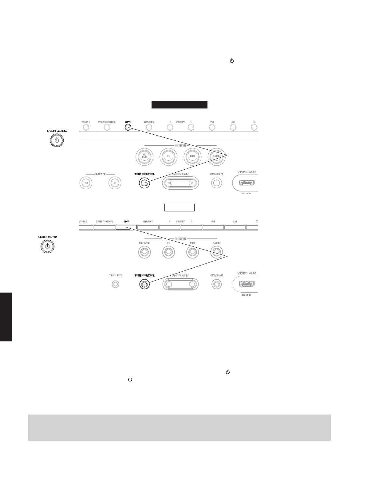
● Starting Self-Diagnostic Function
While pressing the “TONE CONTROL” and “INFO” keys, press the “MAIN ZONE ” key to turn on the power, and release
those 2 keys.
The self-diagnostic function mode is activated.
Keys of this unit
RX-V673/HTR-6065
While pressing these keys, turn on the power.
RX-A720
RX-V673/HTR-6065/
● Starting Self-Diagnostic Function in the protection cancel mode
If the protection function works and causes hindrance to troubleshooting, cancel the protection function by the procedure
below, and it will be possible to enter the self-diagnostic function mode. (The protection functions other than the excess
current detect function will be disabled.)
While pressing the “TONE CONTROL” and “INFO” keys, press the “MAIN ZONE
pressing those 2 keys and “MAIN ZONE
The self-diagnostic function mode is activated with the protection functions disabled.
In this mode, the “SLEEP” segment of the FL display flashes to indicate that the mode is self-diagnostic function mode with the
protection functions disabled.
RX-A720
While pressing these keys, turn on the power.
” key to turn on the power and keep
” key for 3 seconds or longer.
CAUTION!
Using this unit with the protection function disabled may cause further damage to this unit. Use special care for this point
when using this mode.
30

RX-V673/HTR-6065/RX-A720
● Canceling Self-Diagnostic Function
1. Before canceling self-diagnostic function, execute setting for “S3. FACTORY PRESET” menu. (Memory initialization
inhibited or Memory initialized).
* In order to keep the user memory preserved, be sure to select PRESET INHIBIT (Memory initialization inhibited).
2. Press the “MAIN ZONE
” key to turn off the power.
● Display provided when Self-Diagnostic Function started
The display is as described below depending on the situation when the power to this unit is turned off.
1. When the power is turned off by usual operation:
“NO PROTECT” is displayed. Then “A1-1. DSP MARGIN” is displayed in a few seconds.
Main menu displayOpening message
After a few seconds
A1-1
NOPROTECT
DSPMARGIN
2. When the protection function worked to turn off the power:
The information of protection function which worked at that time is displayed. Then “A1-1. DSP MARGIN” is displayed in
a few seconds.
Note: At that time if you restart the self-diagnostic function after turning off the power once, “NO PROTECT” will be
displayed. That is because that situation is equal to “1. When the power is turned off by usual operation:”.
However history of the protection function is stored in memory as backup data. For details, refer to “P2.
PROTECTION HISTORY” menu.
2-1. When there is a history of protection function due to excess current.
IPROTECT
Cause: An excessive current flowed through the power amplifier.
Supplementary information: As over current of the power amplifier is detected, check condition of each power transistor.
Turning on the power without correcting the abnormality will cause the protection function to work immediately and the
power supply will instantly be shut off.
RX-V673/HTR-6065/
RX-A720
Notes:
• Applying the power to this unit without correcting the abnormality can be dangerous and cause additional
circuit damage. To avoid this, if “I PROTECT” protection function works 1 time, the power will not turn on even
when the “MAIN ZONE
function.
• The output transistors in each amplifier channel should be checked for damage before applying power to this
unit.
• Amplifier current should be monitored by measuring DC voltage across the emitter resistors for each channel.
” key is pressed. In order to turn on the power again, start up the self-diagnostic
31

RX-V673/HTR-6065/RX-A720
2-2. When the protection function worked due to abnormal DC output.
H: Displayed when the voltage is HIGHER than upper limit
L: Displayed when the voltage is LOWER than lower limit
DCPRT:xxxH
xxx: A/D conversion value of voltage at the moment when the protection function worked
(Reference voltage: 3.3 V=255)
Cause: DC output of the power amplifier is abnormal.
Supplementary information: The protection function worked due to a DC voltage appearing at the speaker terminal. A
cause could be a defect in the amplifier.
Turning on the power without correcting the abnormality will cause the protection function to work in 5 seconds and the
power supply will be shut off.
2-3. When the protection function worked due to abnormal voltage in the power supply section.
Cause: The voltage in the power supply section is abnormal.
Supplementary information: The protection function worked due to a defect or overload in the power supply.
Turning on the power without correcting the abnormality will cause the protection function to work in 1 seconds and the
power supply will be shut off.
Notes:
RX-A720
RX-V673/HTR-6065/
• Applying the power to this unit without correcting the abnormality can be dangerous and cause additional
circuit damage. To avoid this, if “PS” and “DC” protection function works 3 times consecutively, the power will
not turn on even when the “MAIN ZONE
diagnostic function.
• The output transistors in each amplifier channel should be checked for damage before applying power to this
unit.
• Amplifier current should be monitored by measuring DC voltage across the emitter resistors for each channel.
H: Displayed when the voltage is HIGHER than upper limit
L: Displayed when the voltage is LOWER than lower limit
PSxPRT:xxxL
xxx: A/D conversion value of voltage at the moment when the protection function worked
(Reference voltage: 3.3 V=255)
PS1/PS2/PS3
” key is pressed. In order to turn on the power again, start up the self-
32

RX-V673/HTR-6065/RX-A720
2-4. When the protection function worked due to excessive heatsink temperature.
H: Displayed when the voltage is HIGHER than upper limit
L: Displayed when the voltage is LOWER than lower limit
TMPPRT:xxxL
xxx: A/D conversion value of voltage at the moment when the protection function worked
(Reference voltage: 3.3 V=255)
Cause: The temperature of the heatsink is excessive.
Supplementary information: The protection function worked due to the temperature limit being exceeded. Causes could
be poor ventilation or a defect related to the thermal sensor.
Turning on the power without correcting the abnormality will cause the protection function to work in 1 seconds and the
power supply will be shut off.
● History of protection function
When the protection function has worked, its history is stored in memory as backup data.
Even if no abnormality is noted while servicing the unit, an abnormality which has occurred previously can be defined
as long as the backup data has been stored.
For details, refer to “P2. PROTECTION HISTORY” menu.
RX-V673/HTR-6065/
RX-A720
33

RX-V673/HTR-6065/RX-A720
● Operation procedure of Main menu and Sub-menu
There are 22 main menu items, each of which has sub-menu items.
Main menu selection
Select the main menu using “SCENE TV” (forward) and “SCENE BD/DVD” (reverse) keys.
Sub-menu selection
Select the sub-menu using “SCENE RADIO” (forward) and “SCENE NET” (reverse) keys.
Keys of this unit
Main menu selection
Reverse Forward
Sub-menu selection
Reverse Forward
● Functions in Self-Diagnostic Function mode
In addition to the self-diagnostic function menu items, functions listed below are available.
• Power ON/OFF
• Master volume
• Muting
• Input selection
• Zone control
* Functions related to the tuner and the set menu are not available.
RX-A720
RX-V673/HTR-6065/
● Initial settings when Self-Diagnostic Function started
The following initial settings are used when self-diagnostic function is started.
• Master volume: -20 dB / Zone volume: +2.5dB
• Input: HDMI1 / Zone input: AUDIO1
• Main menu: A1-1. DSP MARGIN
• Speaker setting: LARGE, Bass out to SWFR (All channels)
• HDMI Control: Off
• Zone 2: On
* When self-diagnostic function is canceled, these settings are restored to those before starting self-diagnostic function.
34

● Details of Self-Diagnostic Function menu
A1. DSP AUDIO
This menu is used to check audio signal route via DSP.
A1-1. DSP MARGIN
The audio signal is output including the head margin via DSP.
* When input source is stereo, signal is assigned as below.
Front L: Front L, Center, Surround L, Surround Back L
Front R: Front R, Surround R, Surround Back R
Front L +10 dB: Subwoofer
A1-1
DSPMARGIN
A1-2. DSP NON MARGIN
The SUBWOOFER signal is output including the head margin via DSP.
The audio signal other than SUBWOOFER is output without including the head margin via DSP.
RX-V673/HTR-6065/RX-A720
A1-2
DSPNONMARGIN
A1-3. INVALID ITEM
Not for service.
A1-3
INVALIDITEM
A1-4. DSP FULL CENTER
The audio signal is output to only CENTER channel in digital full bit without including the head margin.
A1-4
DSPFULLC
A1-5. DSP FULL SURROUND
The audio signal is output to only SURROUND L/R channels in digital full bit without including the head margin.
RX-V673/HTR-6065/
RX-A720
A1-5
DSPFULLSUR
35

RX-V673/HTR-6065/RX-A720
A1-6. DSP FULL SURROUND BACK
The audio signal is output to only SURROUND BACK L/R channel in digital full bit without including the head
margin.
A1-7. DSP FULL SUBWOOFER
The audio signal is output to only SUBWOOFER channel in digital full bit without including the head margin.
A1-6
DSPFULLSB
A1-7
DSPFULLSW
A2. DIRECT AUDIO
This menu is used to check audio signal route of PURE DIRECT mode.
A2-1. DIRECT VH
RX-A720
RX-V673/HTR-6065/
A2-2. DIRECT VL
The analog input audio signal is output to FRONT L/R in PURE DIRECT mode.
VH: Voltage High, RY101 on MAIN P.C.B.: Off
A2-1
DIRECT:VH
The analog input audio signal is output to FRONT L/R in PURE DIRECT mode.
VL: Voltage Low, RY101 on MAIN P.C.B.: On
A2-2
DIRECT:VL
36

RX-V673/HTR-6065/RX-A720
A3. HDMI AUDIO
This menu is used to check the route of audio signal input to HDMI IN/OUT jack.
* Before check using “A3-3. ARC 1” menu, be sure to connect a TV monitor equipped with Audio Return Channel
function to this unit in advance.
A3-1
HDMIAUTO
A3-2
INVALIDITEM
A3-3
ARC1
A3-4
INVALIDITEM
A3-5
INVALIDITEM
A3-1. HDMI AUTO
The audio signal input to selectedHDMI IN jack is output.
A3-2. INVALID ITEM
Not for service.
A3-3. ARC 1 (Audio Return Channel function)
The audio signal input to HDMI OUT jack is output.
A3-4. INVALID ITEM
Not for service.
A3-5. INVALID ITEM
Not for service.
RX-V673/HTR-6065/
RX-A720
37

RX-V673/HTR-6065/RX-A720
A4. SPEAKERS SET
This menu is used to check the speaker output.
A4-1
BI-AMP
A4-2
ZONE/TONE=MAX
A4-3
ZONE/TONE=MIN
A4-4
INVALIDITEM
A4-5
INVALIDITEM
A4-6
D-PARTYMODE
A4-1. BI-AMP
The FRONT L/R signal is distributed to SURROUND BACK L/R terminals.
A4-2. ZONE/TONE=MAX
The audio signal is output to FRONT L/R, CENTER and SURROUND L/R terminals with the tone control
“BASS +6 dB”, “TREBLE +6 dB”.
A4-3. ZONE/TONE=MIN
The audio signal is output to FRONT L/R, CENTER and SURROUND L/R terminals with the tone control
“BASS -6 dB”, “TREBLE -6 dB”.
A4-4. INVALID ITEM
Not for service.
A4-5. INVALID ITEM
Not for service.
A4-6. D-PARTY MODE
The FRONT L/R signal is distributed to ZONE2 L/R terminals.
ZONE2 volume: -3.5 dB
A4-7
FULLMUTE
RX-A720
A4-8
INVALIDITEM
RX-V673/HTR-6065/
A4-9
INVALIDITEM
A4-10
INVALIDITEM
A4-7. FULL MUTE
The audio signals are muted at all channels.
A4-8. INVALID ITEM
Not for service.
A4-9. INVALID ITEM
Not for service.
A4-10. INVALID ITEM
Not for service.
38

A5. MULTI CHANNEL INPUT
Not for service.
RX-V673/HTR-6065/RX-A720
A6. MIC CHECK
A6-1. MIC ROUTE CHECK
The audio signal input to the YPAO MIC jack is output to FRONT L and FRONT R channels via A/D-D/A.
A5-1
8ohmMULTICH
A5-2
6ohmMULTICH
A6-1
MICROUTE
RX-V673/HTR-6065/
RX-A720
39

RX-V673/HTR-6065/RX-A720
A7. MANUAL TEST
The test noise generated by built-in noise generator in DSP is output to the channels specified by the sub-menu.
Test noise Test tone
for SUBWOOFER
for other than SUBWOOFER
30 Hz to 80 Hz 50 Hz
pink noise sine wave
500 Hz to 2 kHz 1 kHz
pink noise sine wave
A7-1
TESTALL
A7-2
TESTFRNTL
A7-3
TESTCENTER
A7-4
TESTFRNTR
A7-5
TESTSURRR
A7-1. TEST ALL
The test noise is output to FRONT L/R, CENTER, SURROUND L/R, SURROUND BACK L/R and LFE 1
channels.
A7-2. TEST FRONT L
The test tone is output to FRONT L channel.
A7-3. TEST CENTER
The test tone is output to CENTER channel.
A7-4. TEST FRONT R
The test tone is output to FRONT R channel.
A7-5. TEST SURROUND R
The test tone is output to SURROUND R channel.
A7-6
TESTSBR
RX-A720
RX-V673/HTR-6065/
A7-7
TESTSBL
A7-8
TESTSURRL
A7-9
TESTFPL
40
A7-6. TEST SURROUND BACK R
The test tone is output to SURROUND BACK R channel.
A7-7. TEST SURROUND BACK L
The test tone is output to SURROUND BACK L channel.
A7-8. TEST SURROUND L
The test tone is output to SURROUND L channel.
A7-9. TEST FRONT PRESENCE L
The test tone is output to FRONT PRESENCE L channel.

RX-V673/HTR-6065/RX-A720
A7-10
TESTFPR
A7-11
INVALIDITEM
A7-12
INVALIDITEM
A7-13
TESTLFE1
A7-14
INVALIDITEM
A7-10. TEST FRONT PRESENCE R
The test tone is output to FRONT PRESENCE R channel.
A7-11. INVALID ITEM
Not for service.
A7-12. INVALID ITEM
Not for service.
A7-13. TEST LFE 1 (SUBWOOFER)
The test tone is output to LFE 1 channel.
A7-14. INVALID ITEM
Not for service.
RX-V673/HTR-6065/
RX-A720
41

RX-V673/HTR-6065/RX-A720
D1. FL CHECK
This menu is used to check operation of the FL display.
D1-1. INITIAL DISPLAY
D1-2. ALL SEGMENT OFF
FL display
RX-A720
RX-V673/HTR-6065/
D1-3. ALL SEGMENT ON
* After check, change to next menu at once.
D1-4. CHECK PATTERN 1
Example
Lighting on segments in lattice.
D1-5. CHECK PATTERN 2
NormalShort
42
Segment conditions of the FL tube is checked by turning ON and OFF all segments.
Next, a short between segments next to each other is checked by turning ON and OFF all segments alternately (in
lattice).
(In the above example, the segments in the second row from the top are shorted.)

Z1. ZONE TEST
This menu is used to check audio signal route to ZONE2 OUT jack.
RX-V673/HTR-6065/RX-A720
Z1-1
AV1
Z1-2
AV2
Z1-3
AV3
Z1-4
AV4
Z1-5
AV5
Z1-6
AV6
Z1-1. AV1
Not for service.
Z1-2. AV2
Not for service.
Z1-3. AV3
Not for service.
Z1-4. AV4
Not for service.
Z1-5. AV5
The audio signal input to AV5 jack is output to ZONE 2 OUT jack.
Z1-6. AV6
The audio signal input to AV6 jack is output to ZONE 2 OUT jack.
Z1-7
AUDIO1
Z1-8
AUDIO2
Z1-9
V-AUX
Z1-10
PHONO
Z1-7. AUDIO1
The audio signal input to AUDIO1 jack is output to ZONE 2 OUT jack.
Z1-8. AUDIO2
The audio signal input to AUDIO2 jack is output to ZONE 2 OUT jack.
Z1-9. V-AUX
Not for service.
Z1-10. PHONO
Not for service.
RX-V673/HTR-6065/
RX-A720
43

RX-V673/HTR-6065/RX-A720
U1. USB
This menu is used to check the audio signal route from USB storage device.
U1-1. USB FRONT 1 TRACK
The 1st music file stored in the USB storage device connected to the USB jack is reproduced.
* Copy 2 or more music files from PC to the root folder of the USB storage device in advance.
U1-1
USBF1TRACK
U1-2. USB FRONT 2 TRACK
The 2nd music file stored in the USB storage device connected to the USB jack is reproduced.
U1-2
USBF2TRACK
U1-3. USB_VBUS HIGH POWER
The output current (USB_VBUS) of USB jack is output at up to 2.1A/5V.
N1. NETWORK
This menu is used to check functions related to NETWORK.
Connect between LAN port of broadband router and NETWORK jack of this unit with a network cable.
* When the network condition varies while sub-menu is displayed (e.g., the network is deactivated once), the correct
RX-A720
RX-V673/HTR-6065/
N1-1. IP ADDRESS CHECK
U1-3
USBVBUSHPWR
result will not be displayed.
In that case, once turn off the power to this unit, then start up the self-diagnostic function again and select this
menu.
This menu is used to check that IP address can be obtained.
N1-1
IPADCHK:OK
OK: Connected (IP address obtained)
NG: No traffic / Disconnected
44
N1-2. MAC ADDRESS CHECK
This menu is used to check that MAC address is written.
N1-2
MACADCHK:OK
OK: Normal
NG: Unwritten

N1-3. LINE NOISE 100 MDI
Not for service.
N1-4. LINE NOISE 100 MDIX
Not for service.
N1-5. LINE NOISE 10 MDI
Not for service.
RX-V673/HTR-6065/RX-A720
N1-3
LNMDI100
N1-4
LNMDIX100
N1-5
LNMDI10
N1-6. LINE NOISE 10 MDIX
Not for service.
N1-6
LNMDIX10
N1-7. EXT TEST
Transmission/reception of the NETWORK jack is checked.
With the power turned off, short the pins of the NETWORK jack as shown in the figure below.
Start up the self-diagnostic function and select this menu.
Transmission/reception test is executed and its result is displayed.
Note: Be sure to return the shorted pins to their original condition after executing this test.
12345678
N1-7
EXTTEST:OK
OK: Normal
NG: Abnormal
--: Checking
RX-V673/HTR-6065/
RX-A720
NETWORK jack
N1-8. MAC ADDRESS
Written MAC address is displayed.
N1-8
00A0DExxxxxx
45

RX-V673/HTR-6065/RX-A720
C1. DIGITAL P.C.B. CHECK
This menu is used to check the communication and bus line connection between devices on DIGITAL P.C.B.
C1-1. ALL
The synthetic judgment result of sub-menu C1-2 to C1-8 is displayed.
C1-1
ALL:OK
OK: No error detected
NG: An error is detected
C1-2. BUS FLASH ROM
FLASH ROM (IC77)’s reading/writing are checked.
C1-2
BUSFROM:OK
OK: No error detected
NG: An error is detected
C1-3. BUS FPGA
C1-4. I2C
RX-A720
RX-V673/HTR-6065/
Communication and bus line connection between microprocessor (IC83) and FPGA (IC50) are checked.
C1-3
BUSFPGA:OK
OK: No error detected
NG: An error is detected
The I2C (Inter integrated circuit) bus line connection is checked.
C1-4
0-00---0--0
Error detection of Front HDMI equalizer (IC30)
Error detection of Video decoder (IC21)
0 : No error detected
1 : An error is detected
46
Error detection of HDMI transmitter (IC61)
Error detection of HDMI receiver (IC3)
Error detection of HDMI switcher 1 (IC1)

RX-V673/HTR-6065/RX-A720
C1-5. FPGA RAM
SDRAM (IC53)’s reading/writing are checked.
C1-5
FPGARAM:OK
OK: No error detected
NG: An error is detected
C1-6. BUS DIR1
Communication and bus line connection between microprocessor (IC83) and DIR1 (IC924) are checked.
C1-6
DIR1BUS:OK
OK: No error detected
NG: An error is detected
C1-7. BUS DSP1
Communication and bus line connection between microprocessor (IC83) and DSP1 (IC921) are checked.
C1-8. EEPROM
EEPROM (IC82)'s reading is checked.
C1-9. INVALID ITEM
Not for service.
C1-10. INVALID ITEM
Not for service.
C1-7
DSP1BUS:OK
C1-8
EEPROM:OK
C1-9
INVALIDITEM
OK: No error detected
NG: An error is detected
OK: No error detected
NG: An error is detected
RX-V673/HTR-6065/
RX-A720
C1-11. INVALID ITEM
Not for service.
C1-10
INVALIDITEM
C1-11
INVALIDITEM
47

RX-V673/HTR-6065/RX-A720
C2. NETWORK IC CHECK
This menu is used to check the communication and bus line connection between devices related to network.
C2-1. ALL
The synthetic judgment result of sub-menu C2-2 to C2-5 is displayed.
C2-1
ALL:OKExt.JIG
OK: No error detected
NG: An error is detected
--: Checking
C2-2. LINK CHECK
LAN cable connection is checked.
Connect between NETWORK jack of this unit and LAN port of broadband router with a network cable.
* When the network condition varies while sub-menu is displayed (e.g., the network is deactivated once), the
correct result will not be displayed. In that case, once turn off the power to this unit, then start up the selfdiagnostic function again and select this menu.
When test result using the “C2-2. LINK CHECK” menu is
NG, the sub-menu C2-2 is NG, “Ext. JIG” is displayed.
C2-3. PHY (Ethernet PHYceiver) TEST
RX-A720
RX-V673/HTR-6065/
C2-4. BUS RAM
C2-2
LINKCHK:OK
OK: Normal
NG: Disconnected
--: Checking
Communication and bus line connection between PHY (IC955) and NETWORK microprocessor (IC951) are
checked.
C2-3
PHYTEST:OK
OK: No error detected
NG: An error is detected
--: Checking
Communication and bus line connection between SDRAM (IC952) and NETWORK microprocessor (IC951) are
checked.
48
C2-4
RAMBUS:OK
OK: No error detected
NG: An error is detected
--: Checking

C2-5. APL (Apple) ID CHECK
Apple authentication IC (IC956) device ID is checked.
V1. ANALOG VIDEO CHECK
This menu is used to check the analog video signal route.
RX-V673/HTR-6065/RX-A720
C2-5
APLID:OK
OK: No error detected
NG: An error is detected
--: Checking
V1-1. ANALOG BYPASS
The video signal is converted and output as shown below.
V1-1
ANALOGBYPASS
ANALOG BYPASS
HDMI IN
Component In
Composite In
DIGITAL
IC3
HDMI
Receiver
VIDEO
IC303
Component
Selector
VIDEO
IC307
Composite
Selector
DIGITAL
IC21
VIDEO
Decoder
V1-2. INVALID ITEM
Not for service.
DIGITAL
IC64
FPGA
MUTE
VDEC_N_RST
Transmitter
VIDEO
IC302
Video Driver
VIDEO
IC301
Video Driver
DIGITAL
IC61
HDMI
HDMI OUT
Component Out
RX-V673/HTR-6065/
RX-A720
Composite Out
V1-3. INVALID ITEM
Not for service.
V1-2
INVALIDITEM
V1-3
INVALIDITEM
49

RX-V673/HTR-6065/RX-A720
V1-4. MUTE CHECK
The video signal is muted.
MUTE CHECK
HDMI IN
Component In
DIGITAL
IC3
HDMI
Receiver
VIDEO
IC303
Component
Selector
V1-4
MUTECHECK
DIGITAL
IC21
VIDEO
Decoder
DIGITAL
IC64
FPGA
MUTE
VDEC_N_RST
MUTE
CPNT_N_VMT
Transmitter
VIDEO
IC302
Video Driver
DIGITAL
IC61
HDMI
HDMI OUT
Component Out
V1-5. TEST PATTERN
V1-6. VIDEO INFORMATION
RX-A720
RX-V673/HTR-6065/
VIDEO
IC307
Composite
Composite In
Selector
Not for service.
V1-5
TESTPATTERN
The information of input analog video signals is displayed.
V1-6
VIDIN:480i60
MUTE
VID_N_MMT
VIDEO
IC301
Video Driver
Composite Out
50

V2. DIGITAL VIDEO CHECK
This menu is used to check the digital video signal route.
V2-1. LOOPBACK TEST 1
Execute the test for all HDMI IN jacks by repeating the procedure below.
1. Select sub-menu other than V2-1.
2. Connect between any of the HDMI IN jacks and HDMI OUT jack with an HDMI cable.
3. Select V2-1. The test result is displayed in a few seconds.
CB5
CB4
CB30
HDMI IN
Front
HDMI
IN5
HDMI
IN4
CB3
HDMI
IN3
V2-1
TEST1:OK
HDMI Cable for Loopback
CB2
HDMI
IN2
CB1
HDMI
IN1
RX-V673/HTR-6065/RX-A720
OK: No error detected
NG: An error is detected
--: Checking
CB61
HDMI
OUT1
IC30
Front-HDMI-Board
HDMI EQUALIZER
TMDS261
Y,CbCr
Y,C
CVBS
IC2
HDMI SWITCHER 2
Sii9589-3
IC21
VIDEO DECODER
ADV7180BSTZ
IC3
HDMI RECEIVER
ADV7619
IC1
HDMI SWITCHER 1
Sii9589-3
IC53
128Mbit
SDRAM
IC50
FPGA
EP4CE15F23C6N
IC61
HDMI
TRANSMITTER
Sii9136-3
RX-V673/HTR-6065/
RX-A720
51

RX-V673/HTR-6065/RX-A720
V2-2. LOOPBACK TEST 2
Execute the test for all HDMI IN jacks by repeating the procedure below.
1. Select sub-menu other than V2-2.
2. Connect between any of the HDMI IN jacks and HDMI OUT jack with an HDMI cable.
3. Select the input source corresponding to the connected HDMI IN jack by using “INPUT
keys (RX-V673/HTR-6065) / “INPUT” knob (RX-A720).
4. Select V2-2. The test result is displayed in a few seconds.
Select the input source Result
HDMI1 V-AUX
” and “INPUT ”
V2-2
TEST2:OK
OK: No error detected
NG: An error is detected
--: Checking
HDMI Cable for Loopback
RX-A720
RX-V673/HTR-6065/
CB30
HDMI IN
Front
IC30
Front-HDMI-Board
HDMI EQUALIZER
TMDS261
Y,CbCr
Y,C
CVBS
IC2
HDMI SWITCHER 2
Sii9589-3
IC21
VIDEO DECODER
ADV7180BSTZ
CB5
HDMI
IN5
IC3
HDMI RECEIVER
ADV7619
CB4
HDMI
CB3
HDMI
IN4
IN3
IC1
HDMI SWITCHER 1
Sii9589-3
CB2
HDMI
IN2
CB1
HDMI
IN1
EP4CE15F23C6N
IC53
128Mbit
SDRAM
IC50
FPGA
CB61
HDMI
OUT1
IC61
HDMI
TRANSMITTER
Sii9136-3
4K test pattern 3840x2160/24Hz
52

V2-3. LOOPBACK TEST 3
Execute the test for all HDMI IN jacks by repeating the procedure below.
1. Select sub-menu other than V2-3.
2. Connect between any of the HDMI IN jacks and HDMI OUT jack with an HDMI cable.
3. Select the input source corresponding to the connected HDMI IN jack by using “INPUT
keys (RX-V673/HTR-6065) / “INPUT” knob (RX-A720).
4. Select V2-3. The test result is displayed in a few seconds.
Select the input source Result
HDMI1 V-AUX
RX-V673/HTR-6065/RX-A720
” and “INPUT ”
V2-3
TEST3:OK
OK: No error detected
NG: An error is detected
--: Checking
HDMI Cable for Loopback
CB30
HDMI IN
Front
IC30
Front-HDMI-Board
HDMI EQUALIZER
TMDS261
HDMI SWITCHER 2
Y,CbCr
Y,C
CVBS
VIDEO DECODER
V2-4. INVALID ITEM
Not for service.
IC2
Sii9589-3
IC21
ADV7180BSTZ
CB5
HDMI
IN5
IC3
HDMI RECEIVER
ADV7619
CB4
CB3
HDMI
HDMI
IN4
IN3
IC1
HDMI SWITCHER 1
Sii9589-3
CB2
HDMI
IN2
CB1
HDMI
IN1
EP4CE15F23C6N
IC53
128Mbit
SDRAM
IC50
FPGA
1080/60Hz 12bit
CB61
HDMI
OUT1
IC61
HDMI
TRANSMITTER
Sii9136-3
RX-V673/HTR-6065/
RX-A720
V2-5. INVALID ITEM
Not for service.
V2-6. INVALID ITEM
Not for service.
V2-4
INVALIDITEM
V2-5
INVALIDITEM
V2-6
INVALIDITEM
53

RX-V673/HTR-6065/RX-A720
V2-7. HDMI REPEAT
The video/audio signals input to HDMI IN jack are output to HDMI OUT jack.
V2-7
HDMIREPEAT**
The Deep Color video signals is input, “30” bit or
“36” bit is displayed.
CB30
HDMI IN
Front
IC30
Front-HDMI-Board
HDMI EQUALIZER
TMDS261
Y,CbCr
Y,C
CVBS
HDMI output
HDMI
IC2
HDMI SWITCHER 2
Sii9589-3
IC21
VIDEO DECODER
ADV7180BSTZ
BD/DVD player
CB5
HDMI
IN5
IC3
HDMI RECEIVER
ADV7619
CB4
HDMI
CB3
HDMI
IN4
IN3
IC1
HDMI SWITCHER 1
Sii9589-3
CB2
HDMI
IN2
CB1
HDMI
IN1
EP4CE15F23C6N
IC53
128Mbit
SDRAM
IC50
FPGA
HDMI
TV
CB61
HDMI
OUT1
IC61
HDMI
TRANSMITTER
Sii9136-3
V2-8. DIGITAL CVBS
RX-A720
RX-V673/HTR-6065/
Video output
VIDEO
BD/DVD player
The video (CVBS) signal is converted and output as shown below.
V2-8
DIGITALCVBS
CB5
CB4
CB3
CB2
IN2
CB1
HDMI
IN1
CB30
HDMI IN
Front
IC30
Front-HDMI-Board
HDMI EQUALIZER
TMDS261
Y,CbCr
Y,C
CVBS
IC2
HDMI SWITCHER 2
Sii9589-3
IC21
VIDEO DECODER
ADV7180BSTZ
HDMI
IN5
IC3
HDMI RECEIVER
ADV7619
HDMI
HDMI
IN4
IN3
IC1
HDMI SWITCHER 1
Sii9589-3
HDMI
IC53
128Mbit
SDRAM
IC50
FPGA
EP4CE15F23C6N
HDMI
TV
CB61
HDMI
OUT1
IC61
HDMI
TRANSMITTER
Sii9136-3
54

V2-9. INVALID ITEM
Not for service.
V2-9
INVALIDITEM
V2-10. DIGITAL COMPONENT
The component video (Y, Cb, Cr) signal is converted and output as shown below.
V2-10
DIGITALCmp
RX-V673/HTR-6065/RX-A720
TV
HDMI
HDMI IN
Front-HDMI-Board
HDMI EQUALIZER
TMDS261
Component video output
COMPONENT
BD/DVD player
CB30
Front
IC30
Y,CbCr
Y,C
CVBS
IC2
HDMI SWITCHER 2
Sii9589-3
IC21
VIDEO DECODER
ADV7180BSTZ
CB5
HDMI
IN5
IC3
HDMI RECEIVER
ADV7619
CB4
CB3
HDMI
HDMI
IN4
IN3
IC1
HDMI SWITCHER 1
Sii9589-3
CB2
HDMI
IN2
CB1
HDMI
IN1
EP4CE15F23C6N
IC53
128Mbit
SDRAM
IC50
FPGA
CB61
HDMI
OUT1
IC61
HDMI
TRANSMITTER
Sii9136-3
RX-V673/HTR-6065/
RX-A720
55

RX-V673/HTR-6065/RX-A720
V2-11. DIGITAL COMPONENT SC
The component video (Y, Cb, Cr) signal is converted and output as shown below.
HDMI video output up-scaling: 480i/p, 576i/p only => 1080p
Front-HDMI-Board
HDMI EQUALIZER
Component output
COMPONENT
BD/DVD player
CB30
HDMI IN
Front
IC30
TMDS261
Y,CbCr
Y,C
CVBS
IC2
HDMI SWITCHER 2
Sii9589-3
IC21
VIDEO DECODER
ADV7180BSTZ
CB5
HDMI
IN5
IC3
HDMI RECEIVER
ADV7619
V2-11
DIGITALCmpSC
CB4
HDMI
CB3
HDMI
IN4
IN3
IC1
HDMI SWITCHER 1
Sii9589-3
CB2
HDMI
IN2
CB1
HDMI
IN1
EP4CE15F23C6N
IC53
128Mbit
SDRAM
IC50
FPGA
HDMI
TV
CB61
HDMI
OUT1
IC61
HDMI
TRANSMITTER
Sii9136-3
V2-12. GUI (Graphical User Interface)-VIDEO OUT
RX-A720
RX-V673/HTR-6065/
The GUI is output from FPGA (IC50 on DIGITAL P.C.B.).
V2-12
GUI-VIDEOOUT
CB5
CB4
CB30
HDMI IN
Front
IC30
Front-HDMI-Board
HDMI EQUALIZER
TMDS261
Y,CbCr
Y,C
CVBS
IC2
HDMI SWITCHER 2
Sii9589-3
IC21
VIDEO DECODER
ADV7180BSTZ
HDMI
IN5
IC3
HDMI RECEIVER
ADV7619
HDMI
CB3
HDMI
IN4
IN3
IC1
HDMI SWITCHER 1
Sii9589-3
CB2
HDMI
IN2
CB1
HDMI
IN1
EP4CE15F23C6N
GUI
IC53
128Mbit
SDRAM
IC50
FPGA
HDMI
TV
CB61
HDMI
OUT1
IC61
HDMI
TRANSMITTER
Sii9136-3
56

V3. TEST PATTERN
The video signal is output to HDMI OUT jack with its resolution converted as shown below.
CB5
CB4
CB3
CB2
IN2
CB1
HDMI
IN1
CB30
HDMI IN
Front
HDMI
IN5
HDMI
IN4
HDMI
IN3
HDMI
RX-V673/HTR-6065/RX-A720
TV
HDMI
CB61
HDMI
OUT1
IC30
Front-HDMI-Board
HDMI EQUALIZER
TMDS261
Y,CbCr
Y,C
CVBS
V3-1. 480i
V3-1
480i
V3-5. 1080p 60Hz
V3-5
1080p60
IC2
HDMI SWITCHER 2
Sii9589-3
IC21
VIDEO DECODER
ADV7180BSTZ
IC3
HDMI RECEIVER
ADV7619
V3-2. 480p
V3-2
480p
V3-6. 576i
V3-6
576i
IC1
HDMI SWITCHER 1
Sii9589-3
IC53
128Mbit
SDRAM
IC50
FPGA
EP4CE15F23C6N
GUI
V3-3. 720p 60Hz
V3-3
720p60
V3-7. 576p
V3-7
576p
IC61
HDMI
TRANSMITTER
Sii9136-3
V3-4. 1080i 60Hz
V3-4
1080i60
V3-8. 720p 50Hz
V3-8
720p50
RX-V673/HTR-6065/
RX-A720
V3-9. 1080i 50Hz
V3-9
1080i50
V3-13. 720p 60Hz 3D/FP
V3-13
720p603D/FP
V3-17. 1080i 50Hz 3D/SS
V3-17
1080i503D/SS
V3-21. 4k 24Hz
V3-21
4k24
V3-10. 1080p 50Hz
V3-10
1080p50
V3-14. 720p 50Hz 3D/FP
V3-14
720p503D/FP
V3-18. 720p 60Hz 3D/TB
V3-18
720p603D/TB
(TB: Top-and-Bottom)
(4k: Digital cinema 4K, Resolution 3996 × 2160p)
V3-11. 1080p 24Hz
V3-11
1080p24
V3-12. 1080p 24Hz 3D/FP
V3-12
1080p243D/FP
(FP: Frame Packing)
V3-15. 1080i 60Hz 3D/FP
V3-15
1080i603D/FP
V3-16. 1080i 60Hz 3D/SS
V3-16
1080i603D/SS
(SS: Side-by-Side)
V3-19. 720p 50Hz 3D/TB V3-20. 1080p 24Hz 3D/TB
V3-19
720p503D/TB
V3-20
1080p243D/TB
57

RX-V673/HTR-6065/RX-A720
P1. SYSTEM MONITOR
This menu is used to display the A/D conversion value of the microprocessor which detects panel keys and protection
functions by using the sub-menu.
When “P1-7. KEY1/KEY2” sub-menu is selected, keys become inoperable due to detection of the values of all keys.
However, it is possible to advance to the next menu by pressing the “SCENE RADIO” (forward) key or “SCENE NET”
(reverse) key on the remote control.
* Numeric values in the figure are given as reference only.
P1-1. DC
Power amplifier DC (DC voltage) output is detected.
The voltage at 5 pin (DC_PRT) of IC78 is displayed.
Normal value: 32 to 74
(Reference voltage: 3.3 V=255)
* If DC becomes out of the normal value range, the protection function works to turn off the power.
P1-1
DC:50
P1-2. PS1/PS2/PS3
RX-A720
RX-V673/HTR-6065/
Power supply voltage (PS) protection detection.
The voltage at 2 pin (PS1_PRT)/1 pin (PS2_PRT)/13 pin (PS3_PRT) of IC78 are displayed.
Voltage detects
PS1: ACBL, AC12, AC5, ±7
PS2: -VP, +5T, ±5V
PS3: +5.5V
Normal value
PS1: 12 to 100
PS2: 90 to 166 (PURE DIRECT mode: 143 to 220)
PS3: 132 to 168
(Reference voltage: 3.3 V=255)
* If PS1, PS2 or PS3 becomes out of the normal value range, the protection function works to turn off the
power.
P1-2
PS:77/129/153
PS3
PS2
PS1
58
P1-3. THM
Temperature of the heatsink (THM) is detected.
The voltage at 12 pin (THM1) of IC78 is displayed.
Normal value: 116 to 255 (U, C models)
42 to 255 (R, T, K, A, B, G, F, L, S, H models)
(Reference voltage: 3.3 V=255)
* If THM becomes out of the normal value range, the protection function works to turn off the power.
P1-3
TMa:114

P1-4. INVALID ITEM
Not for service.
P1-5. OUTPUT LEVEL
Output level of speaker output is detected.
The voltage at 4 pin (AMP_OLV) of IC78 is displayed.
(Reference voltage: 3.3 V=255)
RX-V673/HTR-6065/RX-A720
P1-4
INVALIDITEM
P1-5
OUTLVL:255
P1-6. LIMITER CONTROL
Power limitter control is detected.
The voltage at 4 pin (AMP_LMT) of IC83 is displayed.
(Reference voltage: 3.3 V=255)
P1-7. L3 (J model)
Not for service.
P1-6
LMTCNT:255
RX-V673/HTR-6065/
RX-A720
P1-7
L3:4
59

RX-V673/HTR-6065/RX-A720
P1-8. KEY1/KEY2
Panel key is detected.
When the A/D conversion value of the panel key becomes out of the specified range, normal operation will not
be available.
In that case, check the constant of voltage dividing resistor, solder condition, etc. Refer to table.
* When “P1-8. KEY1/KEY2” menu is selected, keys become inoperable due to detection of the values of all
keys. However, it is possible to advance to the next menu by pressing the “SCENE RADIO” (forward) key or
“SCENE NET” (reverse) key on the remote control.
(Reference voltage: 3.3 V=255)
P1-8
KY:254/255
KEY2
KEY1
RX-A720
RX-V673/HTR-6065/
Display KEY1
0 – 11
12 – 32
33 – 54
55 – 75
76 – 96
97 – 119 ZONE2
120 – 142
143 – 172
173 – 202
203 – 235
255 Key off
(RX-V673/HTR-6065 models)
(RX-V673/HTR-6065 models)
RADIO
(SCENE4)
NET
(SCENE3)
TV
(SCENE2)
BD/DVD
(SCENE1)
ZONE
CONTROL
INPUT >
INPUT <
MAIN ZONE
TONE
CONTROL
Display KEY2
0 – 11
12 – 32
33 – 54
55 – 77 AM
78 – 99 FM
100 – 121
122 – 144
145 – 166 MEMORY
167 – 186 INFO
187 – 205 STRAIGHT
206 – 226
227 – 246
255 Key off
PURE
DIRECT
TUNING
>>
TUNING
<<
PRESET
>
PRESET
<
PROGRAM
>
PROGRAM
<
60
P1-9. USB-VBUS
Not for service.
P1-9
USB-VBUS:3

P2. PROTECTION HISTORY
This menu is used to display the history of protection function.
All history of protection function will be erased by pressing the “STRAIGHT” key.
* Numeric values in the figure are given as reference only.
RX-V673/HTR-6065/RX-A720
P2-1
1st:PS2000L
P2-2
2nd:TMP1000L
P2-3
3rd:DC000L
P2-4
NoPrt
P2-1. History 1
H: Displayed when the voltage is HIGHER than upper limit.
L: Displayed when the voltage is LOWER than lower limit.
xxx: A/D conversion value of voltage at the moment when the protection function
worked.
(Reference voltage: 3.3 V=255)
P2-2. History 2
P2-3. History 3
P2-4. History 4
S1. FIRMWARE UPDATE
Not for service.
S1-1
F/WUPDATE?
S2. SET INFORMATION
The model name and destination of this unit are displayed.
S2-1. MODEL
The model name of this unit is displayed.
S2-1
MDL:V673255
RX-V673/HTR-6065/
RX-A720
Not for service.
Model name
V673 : RX-V673
6065 : HTR-6065
A720 : RX-A720
61

RX-V673/HTR-6065/RX-A720
S2-2. DESTINATION
The destination of this unit is displayed.
Destination J U C R (R, S) T K A BG (B, G, F) L (L, H)
A/D conversion value
(3.3 V=255)
S2-3. DEBUG
Not for service.
S2-2
DEST:U28
A/D conversion value
Destination
0 − 12 13 − 39 40 − 67 68 − 92 93 − 115 116 − 140 141 − 169 199 − 221 222 − 244
S2-3
DBG:255
S2-4. NET RESTART COUNTER
S3. FACTORY PRESET
This menu is used to reserve/inhibit initialization of the back-up IC (EEPROM: IC82 on DIGITAL P.C.B.).
RX-A720
RX-V673/HTR-6065/
S3-1
PRESET:INH
S3-1
PRESET:RSRV
Not for service.
S2-4
NRC:0
S3-1. PRESET INHIBIT (Initialization inhibited)
Initialization of the back-up IC is not executed. Select this sub-menu to protect the values set by the user.
S3-1. PRESET RESERVED (Initialization reserved)
Initialization of the back-up IC is reserved. (Actual initialization is executed when the power is turned on
next.) To reset to the original factory settings or to reset the backup IC, select this sub-menu and press
the “MAIN ZONE
” key to turn off the power.
62
CAUTION: Before setting to the PRESET RESERVED, write down the existing preset memory content of the tuner. (This
is because setting to the PRESET RESERVED will cause the user memory content to be erased.)

RX-V673/HTR-6065/RX-A720
S4. ROM VERSION/CHECKSUM
The firmware version and checksum values are displayed.
The checksum is obtained by adding the data at every 8-bit and expressing the result as a hexadecimal notation.
* Numeric values in the figure are given as reference only.
S4-1
SYS-VER.1.10
S4-2
VER.00040
S4-3
SUM.F0EA
S4-4
FR-V.00029
S4-5
FR-S.D2A0
S4-6
S-VER.0041
S4-1. SYSTEM VERSION
The firmware version is displayed.
S4-2. MICROPROCESSOR VERSION
The firmware version of MICROPROCESSOR (IC83 on DIGITAL P.C.B.) is displayed.
S4-3. MICROPROCESSOR CHECKSUM
The checksum value of MICROPROCESSOR (IC83 on DIGITAL P.C.B.) is displayed.
S4-4. FLASH ROM VERSION
The firmware version of FLASH ROM (IC77 on DIGITAL P.C.B.) is displayed.
S4-5. FLASH ROM CHECKSUM
The checksum value of FLASH ROM (IC77 on DIGITAL P.C.B.) is displayed.
S4-6. NETWORK MICROPROCESSOR VERSION
The firmware version of Network microprocessor (IC951 on DIGITAL P.C.B.) is displayed.
S4-7
S-SUM.992245EF
S4-8
D1-V.1.06r3
S4-9
D1-S.47CD49C3
S4-10
INVALIDITEM
S4-7. NETWORK MICROPROCESSOR CHECKSUM
The checksum value of Network microprocessor (IC951 on DIGITAL P.C.B.) is displayed.
S4-8. DSP1 VERSION
The firmware version of DSP1 (IC921 on DIGITAL P.C.B.) is displayed.
S4-9. DSP1 CHECKSUM
The checksum value of DSP1 (IC921 on DIGITAL P.C.B.) is displayed.
S4-10. INVALID ITEM
Not for service.
RX-V673/HTR-6065/
RX-A720
63

RX-V673/HTR-6065/RX-A720
S4-11
INVALIDITEM
S4-12
G-V.000006136
S4-13
FPGA-G-V.18
S4-14
FPGA-S-V.12
S4-15
FPGA-H-V.6
S4-16
INVALIDITEM
S4-11. INVALID ITEM
Not for service.
S4-12. GUI VERSION
The firmware version of GUI data is displayed.
S4-13. FPGA GUI VERSION
The firmware version of GUI section in FPGA (IC50 on DIGITAL P.C.B.) is displayed.
S4-14. FPGA SD (Standard Definition) VERSION
The firmware version of SD I/P scaler section in FPGA (IC50 on DIGITAL P.C.B.) is displayed.
S4-15. FPGA HD (High Definition) VERSION
The firmware version of HD I/P scaler section in FPGA (IC50 on DIGITAL P.C.B.) is displayed.
S4-16. INVALID ITEM
Not for service.
S4-17
INVALIDITEM
RX-A720
RX-V673/HTR-6065/
S4-17. INVALID ITEM
Not for service.
64

RX-V673/HTR-6065/RX-A720
■ POWER AMPLIFIER ADJUSTMENT
1. Right after power is turned on, confirm that the voltage across the terminals of R1152 (SURROUND BACK Rch), R1154
(SURROUND Rch), R1150 (FRONT Rch), R1148 (CENTER), R1149 (FRONT Lch), R1153 (SURROUND Lch) and R1151
(SURROUND BACK Lch) are within the confines of 0.1 mV to 10 mV.
2. If measured voltage exceeds 10 mV, open (cut off) R1104 (SURROUND BACK Rch), R1106 (SURROUND Rch), R1102 (FRONT
Rch), R1100 (CENTER), R1101 (FRONT Lch), R1105 (SURROUND Lch) and R1103 (SURROUND BACK Lch), and then
reconfirm the voltage.
Attention
If the measured voltage exceeds 10 mV after repairing the power amplifier, check other parts again for any possible
defect before cutting the resistor.
3. Confirm that the voltage is within the confines of 0.2 mV to 15 mV after 60 minutes.
0.1 mV – 10 mV
R1154
R1106
(DC)
R1153 R1152
R1105
R1152 (SURROUND BACK Rch)
R1154 (SURROUND Rch)
R1150 (FRONT Rch)
R1148 (CENTER)
R1149 (FRONT Lch)
R1153 (SURROUND Lch)
R1151 (SURROUND BACK Lch)
Front side
R1151
R1104
R1103
Open (cut off)
R1150 R1149
R1102
R1104 (SURROUND BACK Rch)
R1106 (SURROUND Rch)
R1102 (FRONT Rch)
R1100 (CENTER)
R1101 (FRONT Lch)
R1105 (SURROUND Lch)
R1103 (SURROUND BACK Lch)
R1148
R1101
R1100
RX-V673/HTR-6065/
RX-A720
MAIN (1) P.C.B.
65

RX-V673/HTR-6065/RX-A720
■ DISPLAY DATA
● V4001 : 18-MT-11GNK (OPERATION P.C.B.)
RX-V673/HTR-6065
69
PATTERN AREA
● PIN CONNECTION
Pin No.
Connection
Pin No.
Connection
Note : 1) F1, F2 ..... Filament pin 2) NP ..... No pin 3) NX ..... No extend pin 4) 1G-18G ..... Grid pin
● GRID ASSIGNMENT
69
68 67NP66NP65P164P263P362P461P560P659P758P857P956
F2NX
34
P3233P3332P3431P3530P36
18G
1a 1a1a2a 2a2a 2a1a
29 28
NXNX27NX26NX25NX24NX23NX2218G2117G2016G1915G1814G1713G1612G1511 G1410G139G128G117G106G95G84G73G62G51G4NP3NP
17G
S8 S9
P1055P1154P1253P1352P1451P1550P1649P1748P1847P1946P2045P2144P2243P2342P2441P2540P2639P2738P2837P29
16G
17G
1
36
P3035P31
21
F1NX
15G
S7 S5S15 S5
S12
RX-A720
RX-V673/HTR-6065/
66
S11
S10
f
gm
e
2G1G 3G 4G 5G 6G 7G 11G10G9G8G 12G 13G 14G
a
j
b
h
k
nr
c
p
d
(18G–16G)
1-1 2-1 3-1 4-1 5-1
1- 2
2-2
3-2
1- 3
2-3
3-3
1- 4
2-4
3-4
1- 5
2-5
3-5
1- 6
2-6
3-6
1- 7
2-7
3-7
4-2
4-3
4-4
4-5
4-6
4-7
5-2
5-3
5-4
5-5
5-6
5-7
(1G–14G)
S1
S13
S6
a
f
g
e
d
b
c
S2
S3
S3
S4
S2
(15G)

● ANODE CONNECTION
RX-V673/HTR-6065/RX-A720
RX-V673/HTR-6065
P1
P2
P3
P4
P5
P6
P7
P8
P9
P10
P11
P12
P13
P14
P15
P16
P17
P18
P19
P20
P21
P22
P23
P24
P25
P26
P27
P28
P29
P30
P31
P32
P33
P34
P35
P36
18G
1a
1h
1j
1k
1b
1f
1m
1g
1c
1e
1r
1p
1n
1d
2a
2h
2j
2k
2b
2f
2m
2g
2c
2e
2r
2p
2n
2d
S12
S10
S11
17G
1a
1h
1j
1k
1b
1f
1m
1g
1c
1e
1r
1p
1n
1d
2a
2h
2j
2k
2b
2f
2m
2g
2c
2e
2r
2p
2n
2d
S8
S9
S15
–
16G
1a
1h
1j
1k
1b
1f
1m
1g
1c
1e
1r
1p
1n
1d
2a
2h
2j
2k
2b
2f
2m
2g
2c
2e
2r
2p
2n
2d
15G
S5
S7
1d
2d
S2
1e
2e
S3
1c
2c
S4
1g
2g
1f
2f
1b
2b
1a
2a
S6
S13
1G–14G
1-1
2-1
3-1
4-1
5-1
1-2
2-2
3-2
4-2
5-2
1-3
2-3
3-3
4-3
5-3
1-4
2-4
3-4
4-4
5-4
1-5
2-5
3-5
4-5
5-5
1-6
2-6
3-6
4-6
5-6
1-7
2-7
3-7
4-7
5-7
S1
RX-V673/HTR-6065/
RX-A720
67

RX-V673/HTR-6065/RX-A720
● V4001 : HNA-18MM03T (OPERATION P.C.B.)
RX-A720
69
PATTERN AREA
● PIN CONNECTION
Pin No.
Connection
Pin No.
Connection
Note : 1) F1, F2 ..... Filament pin 2) 1G–18G ..... Grid pin 3) P1–P36 ..... Anode pin 4) NP ..... No pin 5) NX ..... No extended pin
● GRID ASSIGNMENT
69
68 67NP66NP65P164P263P362P461P560P659P758P857P956
F2 F2
34
P3233P3332P3431P3530P36
18G
1a 1a1a2a 2a2a
29 28
NXNX27NX26NX25NX24NX23NX2218G2117G2016G1915G1814G1713G1612G1511 G1410G139G128G117G106G95G84G73G62G51G4NP3NP
17G
3a 3b
P1055P1154P1253P1352P1451P1550P1649P1748P1847P1946P2045P2144P2243P2342P2441P2540P2639P2738P2837P29
16G
17G
15G
1
36
P3035P31
21
F1F1
V1 S1S3 S1
A1
RX-A720
RX-V673/HTR-6065/
f
gm
e
68
A3
A2
a
j
h
p
d
(18G–16G)
2G1G 3G 4G 5G 6G 7G 11G10G9G8G 12G 13G 14G
1-1 2-1 3-1 4-1 5-1
1- 2
2-2
2-3
2-4
2-5
2-6
2-7
3-2
3-3
3-4
3-5
3-6
3-7
b
k
nr
c
1- 3
1- 4
1- 5
1- 6
1- 7
4-2
4-3
4-4
4-5
4-6
4-7
5-2
5-3
5-4
5-5
5-6
5-7
V2
V7V6V3
V8V1
V4
V5
U1
(1G–14G)
(15G)
V14
V13
V15
V12
S2
A4
V18
V9
V10
V17
V11
V16
V17
V18

● ANODE CONNECTION
RX-V673/HTR-6065/RX-A720
RX-A720
P1
P2
P3
P4
P5
P6
P7
P8
P9
P10
P11
P12
P13
P14
P15
P16
P17
P18
P19
P20
P21
P22
P23
P24
P25
P26
P27
P28
P29
P30
P31
P32
P33
P34
P35
P36
18G
1a
1h
1j
1k
1b
1f
1m
1g
1c
1e
1r
1p
1n
1d
2a
2h
2j
2k
2b
2f
2m
2g
2c
2e
2r
2p
2n
2d
A1
A2
A3
17G
1a
1h
1j
1k
1b
1f
1m
1g
1c
1e
1r
1p
1n
1d
2a
2h
2j
2k
2b
2f
2m
2g
2c
2e
2r
2p
2n
2d
3a
3b
S3
–
16G
1a
1h
1j
1k
1b
1f
1m
1g
1c
1e
1r
1p
1n
1d
2a
2h
2j
2k
2b
2f
2m
2g
2c
2e
2r
2p
2n
2d
15G
S1
V1
V5
V12
V18
V6
V13
V17
V4
V11
V16
V8
V15
V7
V14
V3
V10
V2
V9
A4
S2
1G–14G
1-1
2-1
3-1
4-1
5-1
1-2
2-2
3-2
4-2
5-2
1-3
2-3
3-3
4-3
5-3
1-4
2-4
3-4
4-4
5-4
1-5
2-5
3-5
4-5
5-5
1-6
2-6
3-6
4-6
5-6
1-7
2-7
3-7
4-7
5-7
U1
RX-V673/HTR-6065/
RX-A720
69

RX-V673/HTR-6065/RX-A720
■ IC DATA
IC921: D80YK113CPTP400 (DIGITAL P.C.B.)
Digital signal processor
Input
Clock(s)
Peripherals
System Control
(Watchdog)
GPIO
eHRPWM
USB2.0
OTG Ctlr
PLL/Clock
Generator
w/OSC
GeneralPurpose
Timer
GeneralPurpose
Timer
Control Timers
eCAP
PHY
JTAG Interface
Memory Protection
I/O Protection
Power/Sleep
Controller
RTC/
OSC
Pin
Multiplexing
32-KHz
Switched Control Resource (SCR)
DMA
EDMA3
eQEP
Connectivity
HPI
dMAX
Audio Ports
MMC/SD
(8b)
McASP
w/FIFO
DSP Subsystem
TM
C674x
DSP MICRO-
PROCESSOR
AET
32 KB
32 KB
L1 Pgm
L1 RAM
256 KB L2 RAM
1024 KB L2 ROM
I2C SPI
External Memory Interface
EMIFA(8b/16b)
NAND/Flash
16b SDRAM
Serial Interface
Shared Memory
128 KB
RAM
EMIFB
SDRAM Only
(16b/32b)
UART
RX-A720
RX-V673/HTR-6065/
70
USB0_VDDA12
USB0_VDDA18
USB0_DP
USB0_DM
USB0_VDDA33
PLL0_VDDA
PLL0_VSSA
OSCIN
OSCVSS
OSCOUT
RESET
RTC_XI
RTC_CVDD
GP7[14]
AHCLKX1/EPWMQB/GP3[14]
ACLKX1/EPWMQA/GP3[15]
AFSX1/EPWMSYNCI/EPWMSYNC0/GP4[10]
ACLKR1/ECAP2/APWM2/GP4[12]
AFSR1/GP4[13]
AXR1[8]/EPWM1A/GP4[8]
AXR1[7]/EPWM1B/GP4[7]
AXR1[6]/EPWM2A/GP4[6]
AXR1[5]/EPWM2B/GP4[5]
AXR1[4]/EQEP1B/GP4[4]
AXR1[3]/EQEP1A/GP4[3]
AXR1[2]/GP4[2]
AXR1[1]/GP4[1]
ACLKX0/ECAP0/APWM0/GP2[12]
AFSX0/GP2[13]/BOOT[10]
AHCLKR0/GP2[14]/BOOT[11]
AFSR0/GP3[12]
ACLKR0/ECAP1/APWM1/GP2[15]
AMUTE1/EHRPWMTZ/GP4[14]
DVDD
128
127
126
132
131
130
129
RSV2
133
134
135
NC
136
137
138
NC
139
140
141
142
143
144
145
146
CVDD
147
148
149
TRST
150
DVDD
151
TMS
152
TDI
153
CVDD
154
TCK
155
TDO
156
157
158
DVDD
159
CVDD
160
161
CVDD
162
163
DVDD
164
165
166
CVDD
167
168
169
170
171
DVDD
172
173
174
175
176
123456789
DD
DV
AXR1[0]/GP4[0]
AXR1[10]/GP5[10]
AXR1[11]/GP5[11]
SPI1_ENA/UART2_RXD/GP5[12]
UART0_RXD/I2C0_SDA/TM64P0_IN12/GP5[8]/BOOT[8]
UART0_TXD/I2C0_SCL/TM64P0_OUT12/GP5[9]/BOOT[9]
AXR0[11]/AXR2[0]/GP3[11]
DVDD
CVDD
119
118
117
116
115
125
124
123
122
1011121314151617181920212223242526272829303132333435363738394041424344
DD
CV
SPI1_SCS[0]/UART2_TXD/GP5[13]
SPI0_CLK/EQEP1I/GP5[2]BOOT[2]
SPI0_SCS[0]/UART0_RTS/EQEP0B/GP5[4]/BOOT[4]
114
121
120
DVDD
EMA_WAIT[0]/UHPI_HRDY/GP2[10]
SPI1_CLK/EQEP1S/GP5[7]BOOT[7]
SPI0_SOMI[0]/EQEP0I/GP5[0]BOOT[0]
SPI0_SIMO[0]/EQEP0S/GP5[1]BOOT[1]
SPI1_SOMI[0]/I2C1/SCL/GP5[5]BOOT[5]
SPI1_SIMO[0]/I2C1/SDA/GP5[6]BOOT[6]
SPI0_ENA/UART0_CTS/EQEP0A/GP5[3]/BOOT[3]
EMB_BA[1]/GP7[0]
EMB_BA[0]/GP7[1]
EMB_CS[0]
EMB_RAS
DVDD
113
112
111
110
109
108
107
106
105
DVDD
CVDD
CVDD
EMA_A[10]/GP1[10]
EMA_BA[0]/GP1[14]
EMA_CS[3]/AMUTE2/GP2[6]
EMA_BA[1]/UHPI_HHWIL/GP1[13]
EMA_OE/UHPI_HDS1/AXR0[13]/GP2[7]
EMA_CS[2]/UHPI_HCS/GP2[5]/BOOT[15]
EMB_A[2]/GP7[4]
EMB_A[1]/GP7[3]
EMB_A[0]/GP7[2]
DVDD
CVDD
9998979695949392919089
104
103
102
101
100
DVDD
EMA_A[0]/GP1[0]
EMA_A[3]/GP1[3]
EMA_A[4]/GP1[4]
EMA_A[5]/GP1[5]
EMA_A[6]/GP1[6]
EMA_A[7]/GP1[7]
EMA_A[1]/MMCSD_CLK/UHPI/HCNTL0/GP1[1]
EMA_A[2]/MMCSD_CMD/UHPI/HCNTL1/GP1[2]
EMB_A[7]/GP7[9]
EMB_A[6]/GP7[8]
EMB_A[5]/GP7[7]
EMB_A[4]/GP7[6]
EMB_A[3]/GP7[5]
EMB_A[10]/GP7[12]
AXR0[0]/AFSR2/GP3[0]
AXR0[1]/ACLKX2/GP3[1]
AXR0[2]/AXR2[3]/GP3[2]
AXR0[3]/AXR2[2]/GP3[3]
AXR0[4]/AXR2[1]/GP3[4]
AXR0[5]/AFSX2/GP3[5]
AXR0[6]/ACLKR2/GP3[6]
AXR0[7]/GP3[7]
AXR0[8]/GP3[8]
UART1_RXD/AXR0[9]/GP3[9]
UART1_TXD/AXR0[10]/GP3[10]
AHCLKX0/AHCLKX2/USB_REFCLKIN/GP2[11]
EMB_A[12]/GP3[13]
EMB_A[11]/GP7[13]
EMB_A[9]/GP7[11]
EMB_A[8]/GP7[10]
DVDD
CVDD
88
EMB_SDCKE
87
DVDD
86
EMB_CLK
85
EMB_WE/DQM[1]/GP5[14]
84
EMB_D[8]/GP6[8]
83
EMB_D[9]/GP6[9]
82
EMB_D[10]/GP6[10]
81
DVDD
80
EMB_D[11]/GP6[11]
79
EMB_D[12]/GP6[12]
78
EMB_D[13]/GP6[13]
77
CVDD
76
EMB_D[14]/GP6[14]
75
DVDD
74
EMB_D[15]/GP6[15]
73
EMB_D[0]/GP6[0]
72
EMB_D[1]/GP6[1]
71
DVDD
70
EMB_D[2]/GP6[2]
69
CVDD
68
EMB_D[3]/GP6[3]
67
CVDD
66
EMB_D[4]/GP6[4]
65
DVDD
64
EMB_D[5]/GP6[5]
63
EMB_D[6]/GP6[6]
62
EMB_D[7]/GP6[7]
61
CVDD
60
EMB_WE_DQM[0]/GP5[15]
59
EMB_WE
58
DVDD
57
EMB_CAS
56
CVDD
55
EMA_WE]/UHPI_HRW/AXR0[12]/GP2[3]/BOOT[14]
54
EMA_D[7]/MMCSD_DAT[7]/UHPI_HD[7]/GP0[7]/BOOT[13]
53
DVDD
52
EMA_D[6]/MMCSD_DAT[6]/UHPI_HD[6]/GP0[6]
51
EMA_D[5]/MMCSD_DAT[5]/UHPI_HD[5]/GP0[5]
50
CVDD
49
EMA_D[4]/MMCSD_DAT[4]/UHPI_HD[4]/GP0[4]
48
EMA_D[3]/MMCSD_DAT[3]/UHPI_HD[3]/GP0[3]
47
DVDD
46
EMA_D[2]/MMCSD_DAT[2]/UHPI_HD[2]/GP0[2]
45
EMA_D[1]/MMCSD_DAT[1]/UHPI_HD[1]/GP0[1]
DVDD
CVDD
EMA_A[8]/GP1[8]
EMA_A[9]/GP1[9]
EMA_A[11]/GP1[11]
EMA_A[12]/GP1[12]
EMA_D[0]/MMCSD_DAT[0]/UHPI_HD[0]/GP0[0]/BOOT[12]

RX-V673/HTR-6065/RX-A720
Pin
No. (1) (2)
1 AXR1[0]/GP4[0] I/O IPD McASP1 serial data
2 UART0_RXD/I2C0_SDA/TM64P0_IN12/GP5[8]/ I IPU BOOT[8]
BOOT[8] I IPU UART0 receive data
3 UART0_TXD/I2C0_SCL/TM64P0_OUT12/GP5[9]/ I IPU BOOT[9]
BOOT[9] O IPU UART0 transmit data
4 AXR1[10]/GP5[10] I/O IPU McASP1 serial data
5 DVDD (I/O supply) PWR 3.3-V I/O supply voltage pins
6 AXR1[11]/GP5[11] I/O IPU McASP1 serial data
7 SPI1_ENA /UART2_RXD/GP5[12] I/O IPU SPI1 enable
8 SPI1_SCS[0] /UART2_TXD/GP5[13] I/O IPU SPI1 chip select
9 SPI0_SCS[0] /UART0_RTS/EQEP0B/GP5[4]/BOOT[4] I/O IPU SPI0 chip select
10 CVDD (Core supply) PWR 1.2-V core supply voltage pins
11 SPI0_CLK/EQEP1I/GP5[2]/BOOT[2] I/O IPD SPI0 clock
12 SPI0_ENA /UART0_CTS/EQEP0A/GP5[3]/BOOT[3] I/O IPU SPI0 enable
13 SPI1_SOMI[0]/I2C1_SCL/GP5[5]/BOOT[5] I/O IPU SPI1 data/slave-out-master-in
14 SPI1_SIMO[0]/I2C1_SDA/GP5[6]/BOOT[6] I/O IPU SPI1 data/slave-in-master-out
15 DVDD (I/O supply) PWR 3.3-V I/O supply voltage pins
16 SPI1_CLK/EQEP1S/GP5[7]/BOOT[7] I/O IPD SPI1 clock
17 SPI0_SOMI[0]/EQEP0I/GP5[0]/BOOT[0] I/O IPD SPI0 data/slave-out-master-in
18 SPI0_SIMO[0]/EQEP0S/GP5[1]/BOOT[1] I/O IPD SPI0 data/slave-in-master-out
19 EMA_WAIT[0]/ UHPI_HRDY/GP2[10] I IPU EMIFA wait input/interrupt
20 CVDD (Core supply) PWR 1.2-V core supply voltage pins
21 EMA_CS[3] /AMUTE2/GP2[6] O IPU EMIFA Async chip select
22 EMA_OE /UHPI_HDS1/AXR0[13]/GP2[7] O IPU EMIFA output enable
23 EMA_CS[2] /UHPI_HCS/GP2[5]/BOOT[15] O IPU EMIFA Async chip select
24 EMA_OE/UHPI_HDS1/AXR0[13]/GP2[7] I/O IPU McASP0 serial data
DVDD (I/O supply) PWR 3.3-V I/O supply voltage pins
25 EMA_BA[0]/ GP1[14] O IPU EMIFA bank address
26 EMA_BA[1]/ UHPI_HHWIL/GP1[13] O IPU EMIFA bank address
Function Name
TYPE PULL
I/O IPU I2C0 serial data
I IPU Timer0 lower input
I/O IPU I2C0 serial clock
O IPU Timer0 lower output
I IPU UART2 receive data
O IPU UART2 transmit data
I IPU eQEP0B quadrature input
I IPU BOOT[4]
O IPU UART0 ready-to-send output
I IPD eQEP1 index
I IPD BOOT[2]
I IPU eQEP0A quadrature input
I IPU BOOT[3]
I IPU UART0 clear-to-send input
I IPU BOOT[5]
I/O IPU I2C1 serial clock
I IPU BOOT[6]
I/O IPU I2C1 serial Data
I IPD eQEP1 strobe
I IPD BOOT[7]
I IPD eQEP0 index
I IPD BOOT[0]
I IPD eQEP0 strobe
I IPD BOOT[1]
I/O IPU UHPI ready
O IPU McASP2 mute output
I/O IPU UHPI data strobe
I IPU BOOT[15]
I/O IPU UHPI chip select
I/O IPU UHPI half-word identification control
Detail of Function
RX-V673/HTR-6065/
RX-A720
71

RX-V673/HTR-6065/RX-A720
Pin
No. (1) (2)
27 EMA_A[10]/ GP1[10] O IPU EMIFA address bus
28 CVDD (Core supply) PWR 1.2-V core supply voltage pins
29 EMA_A[0]/ GP1[0] O IPD EMIFA address bus
30 EMA_A[1]/MMCSD_CLK/UHPI_HCNTL0/GP1[1] O IPU EMIFA address bus
31 EMA_A[2]/MMCSD_CMD/UHPI_HCNTL1/GP1[2] O IPU EMIFA address bus
32 EMA_A[3]/ GP1[3] O IPD EMIFA address bus
33 DVDD (I/O supply) PWR 3.3-V I/O supply voltage pins
34 EMA_A[4]/ GP1[4] O IPD EMIFA address bus
35 EMA_A[5]/ GP1[5] O IPD EMIFA address bus
36 EMA_A[6]/ GP1[6] O IPD EMIFA address bus
37 EMA_A[7]/ GP1[7] O IPD EMIFA address bus
38 CVDD (Core supply) PWR 1.2-V core supply voltage pins
39 EMA_A[8]/ GP1[8] O IPU EMIFA address bus
40 EMA_A[9]/ GP1[9] O IPU EMIFA address bus
41 EMA_A[11]/ GP1[11] O IPU EMIFA address bus
42 EMA_A[12]/ GP1[12] O IPU EMIFA address bus
43 DVDD (I/O supply) PWR 3.3-V I/O supply voltage pins
44 EMA_D[0]/MMCSD_DAT[0]/UHPI_HD[0]/GP0[0]/ I/O IPU EMIFA data bus
BOOT[12] I IPU BOOT[12]
45 EMA_D[1]/MMCSD_DAT[1]/UHPI_HD[1]/GP0[1] I/O IPU EMIFA data bus
46 EMA_D[2]/MMCSD_DAT[2]/UHPI_HD[2]/GP0[2] I/O IPU EMIFA data bus
47 DVDD (I/O supply) PWR 3.3-V I/O supply voltage pins
48 EMA_D[3]/MMCSD_DAT[3]/UHPI_HD[3]/GP0[3] I/O IPU EMIFA data bus
49 EMA_D[4]/MMCSD_DAT[4]/UHPI_HD[4]/GP0[4] I/O IPU EMIFA data bus
RX-A720
RX-V673/HTR-6065/
50 CVDD (Core supply) PWR 1.2-V core supply voltage pins
51 EMA_D[5]/MMCSD_DAT[5]/UHPI_HD[5]/GP0[5] I/O IPU EMIFA data bus
52 EMA_D[6]/MMCSD_DAT[6]/UHPI_HD[6]/GP0[6] I/O IPU EMIFA data bus
53 DVDD (I/O supply) PWR 3.3-V I/O supply voltage pins
54 EMA_D[7]/MMCSD_DAT[7]/UHPI_HD[7]/GP0[7]/ I/O IPU EMIFA data bus
BOOT[13] I IPU BOOT[13]
55 EMA_WE /UHPI_HRW/AXR0[12]/GP2[3]/BOOT[14] O IPU EMIFA SDRAM write enable
56 CVDD (Core supply) PWR 1.2-V core supply voltage pins
57 EMB_CAS O IPU EMIFB column address strobe
58 DVDD (I/O supply) PWR 3.3-V I/O supply voltage pins
59 EMB_WE O IPU EMIFB write enable
60 EMB_WE_DQM[0] /GP5[15] O IPU EMIFB write enable/data mask for EMB_D.
72
Function Name
TYPE PULL
I/O IPU UHPI access control
O IPU MMCSD_CLK
I/O IPU UHPI access control
I/O IPU MMCSD_CMD
I/O IPU UHPI data bus
I/O IPU MMC/SD data
I/O IPU UHPI data bus
I/O IPU MMC/SD data
I/O IPU UHPI data bus
I/O IPU MMC/SD data
I/O IPU UHPI data bus
I/O IPU MMC/SD data
I/O IPU UHPI data bus
I/O IPU MMC/SD data
I/O IPU UHPI data bus
I/O IPU MMC/SD data
I/O IPU UHPI data bus
I/O IPU MMC/SD data
I/O IPU UHPI data bus
I/O IPU MMC/SD data
I IPU BOOT[14]
I/O IPU UHPI read/write
I/O IPU McASP0 serial data
Detail of Function

RX-V673/HTR-6065/RX-A720
Pin
No. (1) (2)
61 CVDD (Core supply) PWR 1.2-V core supply voltage pins
62 EMB_D[7]/GP6[7] I/O IPD EMIFB SDRAM data bus
63 EMB_D[6]/GP6[6] I/O IPD EMIFB SDRAM data bus
64 EMB_D[5]/GP6[5] I/O IPD EMIFB SDRAM data bus
65 DVDD (I/O supply) PWR 3.3-V I/O supply voltage pins
66 EMB_D[4]/GP6[4] I/O IPD EMIFB SDRAM data bus
67 CVDD (Core supply) PWR 1.2-V core supply voltage pins
68 EMB_D[3]/GP6[3] I/O IPD EMIFB SDRAM data bus
69 CVDD (Core supply) PWR 1.2-V core supply voltage pins
70 EMB_D[2]/GP6[2] I/O IPD EMIFB SDRAM data bus
71 DVDD (I/O supply) PWR 3.3-V I/O supply voltage pins
72 EMB_D[1]/GP6[1] I/O IPD EMIFB SDRAM data bus
73 EMB_D[0]/GP6[0] I/O IPD EMIFB SDRAM data bus
74 EMB_D[15]/GP6[15] I/O IPD EMIFB SDRAM data bus
75 DVDD (I/O supply) PWR 3.3-V I/O supply voltage pins
76 EMB_D[14]/GP6[14] I/O IPD EMIFB SDRAM data bus
77 CVDD (Core supply) PWR 1.2-V core supply voltage pins
78 EMB_D[13]/GP6[13] I/O IPD EMIFB SDRAM data bus
79 EMB_D[12]/GP6[12] I/O IPD EMIFB SDRAM data bus
80 EMB_D[11]/GP6[11] I/O IPD EMIFB SDRAM data bus
81 DVDD (I/O supply) PWR 3.3-V I/O supply voltage pins
82 EMB_D[10]/GP6[10] I/O IPD EMIFB SDRAM data bus
83 EMB_D[9]/GP6[9] I/O IPD EMIFB SDRAM data bus
84 EMB_D[8]/GP6[8] I/O IPD EMIFB SDRAM data bus
85 EMB_WE_DQM[1] /GP5[14] O IPU EMIFB write enable/data mask for EMB_D
86 EMB_CLK O IPU EMIF SDRAM clock
87 DVDD (I/O supply) PWR 3.3-V I/O supply voltage pins
88 EMB_SDCKE I/O IPU EMIFB SDRAM clock enable
89 EMB_A[12]/GP3[13] O IPD EMIFB SDRAM row/column address bus
90 DVDD (I/O supply) PWR 3.3-V I/O supply voltage pins
91 EMB_A[11]/GP7[13] O IPD EMIFB SDRAM row/column address bus
92 EMB_A[9]/GP7[11] O IPD EMIFB SDRAM row/column address bus
93 CVDD (Core supply) PWR 1.2-V core supply voltage pins
94 EMB_A[8]/GP7[10] O IPD EMIFB SDRAM row/column address bus
95 EMB_A[7]/GP7[9] O IPD EMIFB SDRAM row/column address bus
96 EMB_A[6]/GP7[8] O IPD EMIFB SDRAM row/column address bus
97 EMB_A[5]/GP7[7] O IPD EMIFB SDRAM row/column address bus
98 EMB_A[4]/GP7[6] O IPD EMIFB SDRAM row/column address
99 DVDD (I/O supply) PWR 3.3-V I/O supply voltage pins
100 EMB_A[3]/GP7[5] O IPD EMIFB SDRAM row/column address
101 EMB_A[2]/GP7[4] O IPD EMIFB SDRAM row/column address
102 EMB_A[1]/GP7[3] O IPD EMIFB SDRAM row/column address
103 EMB_A[0]/GP7[2] O IPD EMIFB SDRAM row/column address
104 CVDD (Core supply) PWR 1.2-V core supply voltage pins
105 EMB_A[10]/GP7[12] O IPD EMIFB SDRAM row/column address bus
106 EMB_BA[1]/GP7[0] O IPU EMIFB SDRAM bank address
107 EMB_BA[0]/GP7[1] O IPU EMIFB SDRAM bank address
108 EMB_CS[0] O IPU EMIFB SDRAM chip select 0
109 DVDD (I/O supply) PWR 3.3-V I/O supply voltage pins
110 EMB_RAS O IPU EMIFB SDRAM row address strobe
111 AXR0[0]/AFSR2/GP3[0] I/O IPD McASP0 serial data
112 AXR0[1]/ACLKX2/GP3[1] I/O IPD McASP0 serial data
113 AXR0[2]/AXR2[3]/GP3[2] I/O IPD McASP0 serial data
114 CVDD (Core supply) PWR 1.2-V core supply voltage pins
115 AXR0[3]/AXR2[2]/GP3[3] I/O IPD McASP0 serial data
Function Name
TYPE PULL
O IPD McASP2 serial data
O IPD McASP2 transmit bit clock
O IPD McASP2 serial data
O IPD McASP2 serial data
Detail of Function
RX-V673/HTR-6065/
RX-A720
73

RX-V673/HTR-6065/RX-A720
Pin
No. (1) (2)
116 AXR0[4]/ AXR2[1]/GP3[4] I/O IPD McASP0 serial data
117 AXR0[5]/AFSX2/GP3[5] I/O IPD McASP0 serial data
118 AXR0[6]/ACLKR2/GP3[6] I/O IPD McASP0 serial data
119 DVDD (I/O supply) PWR 3.3-V I/O supply voltage pins
120 AXR0[7]/GP3[7] I/O IPD McASP0 serial data
121 AXR0[8]/GP3[8] I/O IPU McASP0 serial data
122 UART1_RXD/AXR0[9]/GP3[9] I IPD UART1 receive data
123 UART1_TXD/AXR0[10]/GP3[10] O IPD UART1 transmit data
124 AXR0[11]/ AXR2[0]/GP3[11] I/O IPD McASP0 serial data
125 AHCLKX0/AHCLKX2/USB_REFCLKIN/GP2[11] I/O IPD McASP0 transmit master clock
126 ACLKX0/ECAP0/APWM0/GP2[12] I/O IPD Enhanced capture 0/input or auxiliary PWM 0 output
127 AFSX0/GP2[13]/BOOT[10] I IPD BOOT[10]
128 DVDD (I/O supply) PWR 3.3-V I/O supply voltage pins
129 AHCLKR0/GP2[14]/BOOT[11] I IPD BOOT[11]
130 ACLKR0/ECAP1/APWM1/GP2[15] I/O IPD Enhanced capture 1/input or auxiliary PWM 1 output
131 AFSR0/GP3[12] I/O IPD McASP0 receive frame sync
132 AMUTE1/EPWMTZ/GP4[14] I/O IPD eHRPWM0 trip zone input
133 RSV2 PWR Reserved. For proper device operation, this pin must be tied directly to CVDD
134 USB0_VDDA12 (4) PWR USB0 PHY 1.2-V LDO output for bypass cap
135 USB0_VDDA18 PWR USB0 PHY 1.8-V supply input
136 NC – –
137 USB0_DP A USB0 PHY data plus
RX-A720
RX-V673/HTR-6065/
138 USB0_DM A USB0 PHY data minus
139 NC – –
140 USB0_VDDA33 PWR USB0 PHY 3.3-V supply
141 PLL0_VDDA PWR PLL analog VDD (1.2-V filtered supply)
142 PLL0_VSSA GND PLL analog VSS (for filter)
143 OSCIN I Oscillator input
144 OSCVSS GND Oscillator ground (for filter only)
145 OSCOUT O Oscillator output
146 RESET I Device reset input
147 CVDD (Core supply) PWR 1.2-V core supply voltage pins
148 RTC_XI I Low-frequency (32-kHz) oscillator receiver for real-time clock
149 RTC_CVDD PWR RTC module core power ( isolated from rest of chip CVDD)
150 TRST I IPD JTAG test reset
151 DVDD (I/O supply) PWR 3.3-V I/O supply voltage pins
152 TMS I IPU JTAG test mode select
153 TDI I IPU JTAG test data input
154 CVDD (Core supply) PWR 1.2-V core supply voltage pins
155 TCK I IPU JTAG test clock
156 TDO O IPD JTAG test data output
157 GP7[14] (5) I/O IPD General-Purpose IO signal
158 DVDD (I/O supply) PWR 3.3-V I/O supply voltage pins
159 CVDD (Core supply) PWR 1.2-V core supply voltage pins
74
Function Name
TYPE PULL
O IPD McASP2 serial data
O IPD McASP2 transmit frame sync
I/O IPD McASP2 receive bit clock
(3) I/O IPD McASP0 serial data
(3) I/O IPD McASP0 serial data
O IPD McASP2 serial data
O IPD McASP2 transmit master clock
I IPD USB_REFCLKIN. Optional 48 MHz clock input
I/O IPD McASP0 transmit bit clock
I/O IPD McASP0 transmit frame sync
I/O IPD McASP0 receive master clock
I/O IPD McASP0 receive bit clock
I/O IPD eHRPWM1 trip zone input
I/O IPD eHRPWM2 trip zone input
O IPD McASP1 mute output
Detail of Function

RX-V673/HTR-6065/RX-A720
Pin
No. (1) (2)
160 AHCLKX1/EPWM0B/GP3[14] I/O IPD eHRPWM0 B output
161 CVDD (Core supply) PWR 1.2-V core supply voltage pins
162 ACLKX1/EPWM0A/GP3[15] I/O IPD eHRPWM0 A output
163 AFSX1/EPWMSYNCI/EPWMSYNCO/GP4[10] I/O IPD Sync input to eHRPWM0 module or sync output to external PWM
164 DVDD (I/O supply) PWR 3.3-V I/O supply voltage pins
165 ACLKR1/ECAP2/APWM2/GP4[12] I/O IPD enhanced capture 2/input or auxiliary PWM 2 output
166 AFSR1/GP4[13] I/O IPD McASP1 receive frame sync
167 CVDD (Core supply) PWR 1.2-V core supply voltage pins
168 AXR1[8]/EPWM1A/GP4[8] I/O IPD eHRPWM1 A (with high-resolution)
169 AXR1[7]/EPWM1B/GP4[7] I/O IPD eHRPWM1 B
170 AXR1[6]/EPWM2A/GP4[6] I/O IPD eHRPWM2 A (with high-resolution)
171 AXR1[5]/EPWM2B/GP4[5] I/O IPD eHRPWM2 B
172 DVDD (I/O supply) PWR 3.3-V I/O supply voltage pins
173 AXR1[4]/EQEP1B/GP4[4] I IPD eQEP1B quadrature input
174 AXR1[3]/EQEP1A/GP4[3] I IPD eQEP1A quadrature input
175 AXR1[2]/GP4[2] I/O IPD McASP1 serial data
176 AXR1[1]/GP4[1] I/O IPD McASP1 serial data
Function Name
TYPE PULL
I/O IPD McASP1 transmit master clock
I/O IPD McASP1transmit bit clock
I/O IPD McASP1 transmit frame sync
I/O IPD McASP1 receive bit clock
I/O IPD McASP1 serial data
I/O IPD McASP1 serial data
I/O IPD McASP1 serial data
I/O IPD McASP1 serial data
I/O IPD McASP1 serial data
I/O IPD McASP1 serial data
Detail of Function
(1) I = Input, O = Output, I/O = Bidirectional, Z = High impedance, PWR = Supply voltage, GND = Ground, A = Analog signal.
Note: The pin type shown refers to the input, output or high-impedance state of the pin function when configured as the the signal name highlighted
in bold. All multiplexed signals may enter a high-impedance state when the configured function is input-only or the configured function supports
high-Z operation. All GPIO signals can be used as input or output. For multiplexed pins where functions have different types (ie., input versus
output), the table reflects the pin function direction for that particular peripheral.
(2) IPD = Internal Pulldown resistor, IPU = Internal Pullup resistor
(3) 122, 123 pin: As these signals are internally pulled down while the device is in reset, it is necessary to externally pull them high with resistors if UART1
boot mode is used.
(4) 134 pin: Core power supply LDO output for USB PHY. This pin must be connected via a 0.22-mF capacitor to VSS. When the USB peripheral is not
used, the USB_VDDA12 signal should still be connected via a 1-mF capacitor to VSS.
(5) 157 pin: GP7[14] is initially configured as a reserved function after reset and will not be in a predictable state. This signal will only be stable after
the GPIO configuration for this pin has been completed. Users should carefully consider the system implications of this pin being in an
unknown state after reset.
RX-V673/HTR-6065/
RX-A720
75

RX-V673/HTR-6065/RX-A720
IC951: DM860A (DIGITAL P.C.B.)
Network microprocessor
* No replacement part available.
RESET, BOOT_SEL
4xAudio, 1xVideo
4xAudio
2xAudio
2xAudio
Audio
Memory Bus,
System Extension
LCD
USB
UART
SPI
Security Engine
Reset, Boot, OTP
AV0 Port
2
S, I8S, DSD, video
I
AV2 Port
2
I
S, I8S, DSD
AV3 Port
2
I
S, I8S, DSD,
SPDIF
AV4 Port
2
I
S, I8S, DSD,
SPDIF, ADAT
stereo
PWM-DAC
SD/SRAM and System
Extension Controller
LCD Controller
USB 2.0
USB
OTG
8 kByte RAM
PHY
2 x UART-1
SPI
General Purpose
on-chip RAM
slave
slave
slave
slave
slave
slave
64 kBytes
S
Y
S
T
E
M
B
U
S
master
slave
master
slave
master
slave
master
slave
master
slave
slave
Timing Engine
2 PLLs, 3 DCOs
DMA
2 Forwarding Units
64 Contexts
ARM 926EJ-S
240 MHz
I-cache 16 kByte
D-cache 16 kByte
Interrupt Controller
Watchdog, 2 Timer
RTSP Processor
160 MHz
I-cache 16 kByte
TCM 48 kByte
Audio Engine
160 MHz
I-cache 4 kByte
TCM 10 kByte
Ethernet MAC
10/100 Mbps
NAND FLASH
SSM Controller
CLOCKS
GPIO
(R/SSS)MII
NAND
SSM
RX-A720
RX-V673/HTR-6065/
76
123456789101112131415161718
USBDN
A
USBDP
B
VSS12
C SSMD2
USB
VDD12
D
USB
VSS33
E
RTC
VDD33
F
RTC
VDD12
G
DCO
VSS12
H
DCO
J
PDOUT1
PDOUT0
K
L
AV0CLK
AV0
M D4VSSVS S VSSVSS VSSVSS
CTRL0
AV0
N D8VSSVSS VSSVSS VSSVSS
DATA2
AV1
P
DATA2
AV2CLK
R
AV2
T
CTRL0
AV2
U
DATA0
V NC
123456789101112131415
VDD33
USBC
VDD33
USBT
USBREXT
USBVBUS
USBID
RTCXIN
RTCXOUT
VSS12
PLL
VCO1
VCO0
AOUTLN
AV0
CTRL1
AV0
DATA1
AV1
DATA1
AV2
CTRL1
AV2
DATA1
AV3
CTRL0
AV4
DATA0
VSS33
USBC
VSS33
USBT
USBXO
USBXI
NRES33
USBATST
USBVB
USDRV
VDD33
PLL
VSS33
PLL
VDD12
PLL
XTALO
AOUTLP
XTALI
AOUTRP
AOUTRN
AV0
DATA3
CTRL2
AV0
DATA3
DATA0
AV1
DATA0
DATA3
AV2
AV3CL
DATA2
AV3
AV3
CTRL1
DATA0
AV4
LCDD16 LCDD13 LCDD9
DATA1
LCDD17
LCDD15 LCDD12 LCDD8
OUT
AV0
AV1
AV2
TDO
TDI
HIGHZ
n.c.
VSS RFCLKN SSMD1 SSMD5 TXD1n.c. n.c. RFRXINRFRXQN
NRES12
VSS
OUT
NRES33
NRES12
REF
REF
NC
NC
NC
NC
VDD12
CORE
VDD33IO
VSS
VDD33IO
VDD12
CORE
VDD12
CORE
VSS
VDD33IO
VSS VSS
VDD33IO
VDD12
VSS
CORE
VDD12
VSS
CORE
VDD33IO VDD33IO VDD33IO VDD33IO
AV3
K
LCDD11
DATA1
n.c.
RREF
VDD33
VDD12
CORE
VSSVSS
VSS
VSSVSS
VSSVSS
VSS
VSS
VSS
LCDD7 FD3
LCDD6LCDD14 LCDD10
LCDD5
LCDD4
n.c.
VDD12
SSMWP
VDD33IO VDD3 3IO
VSSVS S VSSVSS VSSVSS
VSSVS S VSSVSS VSSVSS
VDD12
VDD12
CORE
CORE
LCD
LCDD3
CTRL0
LCD
LCDD2
CTRL1
LCD
LCDD1
CTRL2
LCD
LCDD0
CTRL3
SSMD0 SSMD4 SSMCMDn.c. VDD33 RFCLKP RFRXIPRFRXQP
SSMCLK
SSMCP
VDD12
CORE
VSS A22
VSS
VPP MIITXEN MIITXC LK MIIRXER MIICRS FD2
MIITXD0
SSMD6 TCK
SSMD3
SSMD7
VDD12
CORE
VDD12
CORE
MIITXD2
MIIRXD0
VSSNC
TXD0
NRESET
VDD33IOVDD33IO
VSSVSS
VSSVSS
VDD12
CORE
MIIRXD2
RXD1
RXD0 A2TEST1
SPIDI
VDD12
CORE
VDD12
CORE
VDD33IO
VDD33IO
VDD12
CORE
VDD12
CORE
VDD33IO
VDD33IO
MII
RXDV
MIIMDIO
TMS
SPINCS0
SPIDO A7
A9
A13_RAS A14_CAS
A17_DQ M0A18_DQ
A21
NCS0 NCS1
MEMCLK NWE
D3 D2
D7 D6
D11 D10
FD0 FD1
FD5
NFCE0
MIIPHY
CLK
A0
SPICLK
SPINCS1
A3
A4A1A5
A6 A8
A10
A11 A12
A15_BA0 A16_BA1
A19
M1
A23
NCS2
NOE
D1
D5
D9
D13
FD4
FD7
FD6LCDCLK MIIRXCLK MIICOLMIIITXER
FCLE
NFWE
NFWP
NFREMIITXD1 MIIRXD1 MIIRXD3MIITXD3 FALEMIIMDC
16 17 18
A
B
C
D
E
F
A20
G
NCS3VSSVSS VSS
H
MEMCKEVSSVSS VSSVSS VSS
J
NWAITVSSVS S VSS
K
D0VSSVS S VSSVSS VSSVSS
L
M
N
D12
P
D14
R
D15
T
NFRB
U
V
AV-P ort 0
Pin No. Function Name I/O Detail of Function
M4
N1
N2 Several formats are supported.
N3
N4 Video data, together with AV0DATA[3:0]:
P1
P2 AV1DATA[3:0] = video[7:4]
P3
L1 AV0CLK I/O
M1 AV0CTRL0 I/O • Serial audio formats: LRCK input or output.
M2 AV0CTRL1 I/O • Serial audio formats: Master clock output.
M3 AV0CTRL2 I/O
AV-P ort 2
Pin No. Function Name I/O Detail of Function
P4
R3
T2 Several formats are supported.
U1
R1 AV2CLK I/O
T1 AV2CTRL0 I/O
R2 AV2CTRL1 I/O
AV-P ort 3
Pin No. Function Name I/O Detail of Function
R5
T4 Several formats are supported.
R4 AV3CLK I/O
U2 AV3CTRL0 I/O
T3 AV3CTRL1 I/O
AV-P ort 4
Pin No. Function Name I/O Detail of Function
U3
V2 Several formats are supported.
PWM-DAC
Pin No. Function Name I/O Detail of Function
K4 AOUTLP O Left channel PWM output (positive).
L2 AOUTLN O Left channel PWM output (negative).
L4 AOUTRP O Right channel PWM output (positive).
L3 AOUTRN O Right channel PWM output (negative).
UART Interface
Pin No. Function Name I/O Detail of Function
B14 RXD0 I UART-0 receive signal.
C13 TXD0 O UART-0 transmit signal.
A14 RXD1 I UART-1 receive signal.
B13 TXD1 O UART-1 transmit signal.
AV0DATA[3:0] I/O
AV1DATA[3:0] I/O
AV2DATA[3:0] I/O
AV3DATA[1:0] I/O
AV4DATA[1:0] I/O
Audio/video data.
AV0DATA[3:0] = video[3:0]
Data clock. Depending on the AV-Port 0 configuration, this clock is a bit- or byte-clock which is used to
transmit or receive the AV0DATA[*] synchronously.
Configurable sync signal:
• Video formats: PSYNC input or output.
Configurable sync signal:
• Video formats: DVALID input or output.
Configurable sync signal:
• Video formats: FSYNC input or output.
Audio data.
Data clock. Depending on the AV-Port 2 configuration this clock is a bit-clock which is used to transmit or
receive the AV2DATA[*] synchronously.
Configurable sync signal:
Serial audio formats: LRCK input or output.
Configurable sync signal:
Serial audio formats: Master clock output.
Audio data.
Data clock. Depending on the AV-Port 3 configuration this clock is a bit-clock which is used to transmit or
receive the AV3DATA[*] synchronously.
Configurable sync signal:
Serial audio formats: LRCK input or output.
Configurable sync signal:
Serial audio formats: Master clock output.
Audio data.
RX-V673/HTR-6065/RX-A720
RX-V673/HTR-6065/
RX-A720
77
RX-V673/HTR-6065/RX-A720
Serial Peripheral Interface (SPI)
Pin No. Function Name I/O Detail of Function
D14 SPIDIN I SPI data receive.
D15 SPIDOUT O SPI data transmit.
B16 SPICLK I/O SPI clock.
C15 SPINCS0 I/O Master only mode: Chip-select 1 output.
B17 SPINCS1 I/O Master only mode: Chip-select 2 output.
External Memory Interface
Pin No. Function Name I/O Detail of Function
T18
R18
P17
P18
N15
N16
N17
N18
M15
M16
M17
M18
L15
L16
L17
L18
E18
E17
E16
E15
D18
D17
D16 A[12:0] O Address bus for external memory and peripheral access.
C18
C17
RX-A720
RX-V673/HTR-6065/
C16
B18
A18
A17
F15 A13_RAS O
F16 A14_CAS O
F17 A15_BA0 O
F18 A16_BA1 O
G15 A17_DQM0 O
G16 A18_DQM1 O
H17
H16
H15 A[23:19] O Address bus for external memory and peripheral access.
G18
G17
Multi-master mode: Chip-select input (used to detect bus conflict).
Slave mode: Chip-select input.
Multi-master mode: Chip-select 2 output.
Slave mode: Not used.
D[15:0] I/O Data bus for external memory and peripheral access.
SRAM: Address output
SDRAM: Row access strobe
SRAM: Address output
SDRAM: Column access strobe
SRAM: Address output
SDRAM: Bank select
SRAM: Address output
SDRAM: Bank select
SRAM: Address output
SDRAM: Data mask
SRAM: Address output
SDRAM: Data mask
78

RX-V673/HTR-6065/RX-A720
Pin No. Function Name I/O Detail of Function
H18 Chip select signals. The active memory range for NCS[n] (active low) can be configured.
J17 • NCS[0] supports SRAM, can be used for booting.
J16 NCS[3:0] O • NCS[1] supports SDRAM or SRAM.
J15 • NCS[2] supports SRAM.
• NCS[3] supports SRAM.
K17 NOE O Output enable, asserted (low) for read operations.
K16 NWE O Write enable, asserted (low) for write operations.
K18 NWAIT I
K15 MEMCLK O SDRAM system clock.
J18 MEMCKE O SDRAM clock enable.
NAND-Flash Interface
Pin No. Function Name I/O Detail of Function
T17
T16
T15
R17
R16
R15
P16
P15
V18 FALE O Address latch enable; pull-up/down defines boot mode.
U16 FCLE O Command latch enable; pull-up/down defines boot mode.
U15 NFCE0 O Chip-enable, low-active.
U18 NFRB I Ready/busy. NAND flash is busy when NFRB is low.
V17 NFRE O Read enable, low-active.
U17 NFWE O Write enable, low-active.
V16 NFWP O Write protect, low-active.
FD[7:0] I/O Bi-directional data bus.
External wait line. If NWAIT is asserted, memory access will be stalled. Can be configured as either lowactive (default) or high-active.
Ethernet MAC-Phy Interface (MII)
Pin No. Function Name I/O MII RMII SMII
U14 MIIDIO I/O Management data Management data
V14 MIIMDC O Management clock Management clock
V13 MIIRXD[3] I RxD 3 RxD 1
U13 MIIRXD[2] I RxD 2 RxD 0
V12 MIIRXD[1] I RxD 1 Rx-Sync
U12 MIIRXD[0] I RxD 0 RxD
T12 MIIRXCLK I Receive clock Receive clock
R13 MIIRXER I Receive error Receive error
T14 MIIRXDV I Receive data valid Carrier sense/data valid
V11 MIITXD[3] O TxD 3 TxD 1
U11 MIITXD[2] O TxD 2 TxD 0
V10 MIITXD[1] O TxD 1 Tx-Sync
U10 MIITXD[0] O TxD 0 TxD
R12 MIITXCLK I Transmit clock Transmit clock
T11 MIITXER O Transmit error
R11 MIITXEN O Transmit data enable Transmit data enable
T13 MIICOL I MII ethernet collision
R14 MIICRS I MII carrier sense
V15 MIIPHYCLK O 25.000 MHz clock 50.000 MHz clock 125.000 MHz clock
RX-V673/HTR-6065/
RX-A720
79

RX-V673/HTR-6065/RX-A720
USB 2.0 OTG
Pin No. Function Name I/O Detail of Function
B1 USBD+ I/O Positive data line that is connected to the serial USB cable.
A1 USBD– I/O Negative data line that is connected to the serial USB cable.
E2 USBID I USB ID pin of mini-AB receptacle.
C2 USBREXT I External bias resistor (2K7, 1%); connect resistor to VSSUSB.
D2 USBVBUS I VBUS voltage sense.
E3 USBVBUSDRV O Control signal to control VBUS 5V voltage source.
C4 USBXTALI I Oscillator circuit input for a 24.000 MHz crystal (optional).
Without external crystal, pull this pin to GND.
C3 USBXTALO O Oscillator circuit output for a 24.000 MHz crystal (optional).
Without external crystal, leave this pin open.
D3 USBATST – Do not connect.
Power-on Reset Pins
Pin No. Function Name I/O Detail of Function
D6 NRES12REF I Voltage reference input. NRES12OUT is release when this input voltage exceeds VTH12.
C5 NRES12OUT O Open-drain reset (active low) for 1.2V core power supply.
D5 NRES33REF I Voltage reference input. NRES33OUT is release when this input voltage exceeds VTH33.
D4 NRES33OUT O Open-drain reset (active low) for 3.3V core power supply
Real-Time Clock (RTC) Pins (RTC is Not Supported)
Pin No. Function Name I/O Detail of Function
F2 RTCXIN I No connection. Leave this pin open circuit.
G2 RTCXOUT O No connection. Leave this pin open circuit.
F1 VDD33RTC Power No connection. Leave this pin open circuit.
E1 VSS33RTC Power Ground (0 V) for RTC
LCD Interface
Pin No. Function Name I/O TFT Mode LCD STN monochr.
V3 LCDD[17] O RED5
U4 LCDD[16] O RED4
V4 LCDD[15] O RED3
T5 LCDD[14] O RED2
RX-A720
RX-V673/HTR-6065/
U5 LCDD[13] O RED1
V5 LCDD[12] O (RED0)
R6 LCDD[11] O GREEN5
T6 LCDD[10] O GREEN4
U6 LCDD[9] O GREEN3
V6 LCDD[8] O GREEN2
R7 LCDD[7] O GREEN1 DATAHIGH3 DATA7 DATA7
T7 LCDD[6] O GREEN0 DATAHIGH2 DATA6 DATA6
U7 LCDD[5] O BLUE5 DATAHIGH1 DATA5 DATA5
V7 LCDD[4] O BLUE4 DATAHIGH0 DATA4 DATA4
R8 LCDD[3] O BLUE3 DATA3 DATALOW3 DATA3 DATA3
T8 LCDD[2] O BLUE2 DATA2 DATALOW2 DATA2 DATA2
U8 LCDD[1] O BLUE1 DATA1 DATALOW1 DATA1 DATA1
V8 LCDD[0] O (BLUE0) DATA0 DATALOW0 DATA0 DATA0
T10 LCDCLK O Byte clock CL2 CL2 CL2 CL2
V9 LCDCTRL[3] O Display off Display off Display off Display off Display off
U9 LCDCTRL[2] O Vsync FLM FLM FLM FLM
T9 LCDCTRL[1] O HSync CL1 CL1 CL1 CL1
R9 LCDCTRL[0] O DVALID M/Bias
LCD STN monochr.
(double)
LCD STN color
LCD STN color
(bias)
80

SSM Interface
Pin No. Function Name I/O Detail of Function
D12
C12
B12
A12
D11
C11
B11
A11
C10 SSMCLK O Clock output.
A13 SSMCMD O Command output.
D10 SSMCP I Card power input (high = off).
D9 SSMWP I Write protect input (low = protect).
External PLL Pins
Pin No. Function Name I/O Detail of Function
J2
K2
J1
K1 Each of them can be used to feed the loop-filter of a PLL structure.
SSMD[7:0] I/O Data lines.
VCO[1:0] I
PDOUT[1:0] O
External oscillator inputs, typically coming from an external VCO. Together with the external loop-filter and
the internal clock dividers, each PDOUT/VCO pair can form a complete PLL.
Phase discriminator outputs. These signals are charge-pump type outputs.
RX-V673/HTR-6065/RX-A720
Global Pins
Pin No. Function Name I/O Detail of Function
Reset (active low). When asserted, the chip is placed in the reset state and the peripheral pins are
D13 NRESET I
K3 XTALI I Oscillator circuit input. Internal system clock will be derived from XTALI (internal clock multiplier).
J3 XTALO O Oscillator circuit output.
C7 RREF I Reference current. Connect a 3.0 k-ohms ±1% resistor to GND.
B10 TEST1 I Reserved. Connect to VDD for normal operation.
A10 HIGHZ I Reserved. Connect to VDD for normal operation.
E4
F4
G4
H4
J4
V1
A4
A5
B4
B5
C8
C9
JTAG Interface
Pin No. Function Name I/O Detail of Function
B15 TMS I JTAG mode select.
C14 TCK I JTAG clock.
A16 TDI I JTAG serial data input.
A15 TDO O JTAG serial data output.
n.c. – Pins must be left unconnected (18x).
configured as inputs. After deassertion of NRESET, the chip is clocked by XTALI and starts booting from the
port configured by the FCLE, FALE pins.
The NRESET signal must be asserted after power-up.
RX-V673/HTR-6065/
RX-A720
81

RX-V673/HTR-6065/RX-A720
Power Supply Pins
Pin No. Function Name Detail of Function
A6
E8
E9
E12
E13
F5
G5
H14
J14
K5
L5
M14
N14
P6
P7
P10
P11
D7
F6
F7
F8
F9
F10
F11
F12
F13
G6
G7
G8
G9
G10
G11
G12
G13
H6
H7
H8
RX-A720
RX-V673/HTR-6065/
H9 VSS Ground (0 V).
H10
H11
H12
H13
J6
J7
J8
J9
J10
J11
J12
J13
K6
K7
K8
K9
K10
K11
K12
VDD33 I/O power supply (+3.3 V).
Pin No. Function Name Detail of Function
K13
L6
L7
L8
L9
L10
L11
L12
L13
M6
M7
M8
M9
M10 VSS Ground (0 V).
M11
M12
M13
N6
N7
N8
N9
N10
N11
N12
N13
B6
C6
R10 VPP
A2
B2 Power supply (+3.3 V) for USB interface.
A3
B3
F3 VDD33PLL Power supply (+3.3V) for PLL.
G3 VSS33PLL Ground (0 V).
E6
E7
E10
E11
F14
G14
H5
J5
K14 VDD12 Power supply (+1.2V).
L14
M5
N5
P8
P9
P12
P13
D8
D1 VDD12USB Power supply (+1.2V) for USB interface.
C1 VSS12USB Ground (0 V).
H3 VDD12PLL Power supply (+1.2V) for PLL.
H2 VSS12PLL Ground (0 V).
G1 VDD12DCO Power supply (+1.2V) for DCO.
H1 VSS12DCO Ground (0 V).
VDD33USB
VSS33USB
Ground (0 V).
82

IC83: R5F6416MADFE (DIGITAL P.C.B.)
Microprocessor
* No replacement part available.
RX-V673/HTR-6065/RX-A720
D[8]
D[7]
D[6]
D[5]
D[4]
P19_1
P11_4
P19_0
P11_3
P11_2
P11_1
P11_0
P18_7
P18_6
P18_5
P18_4
P18_3
P18_2
D[3]
D[2]
D[1]
D[0]
P15_7
P15_6
P15_5
P15_4
P15_3
P15_2
IIO0_1
VSS
P15_0
VCC
P10_7
AN_6
AN_5
P10_4
P10_3
AN_2
AN_1
AVSS
P10_0
VREF
AVCC
SCL4/RXD4
8 8 8 8 8 8 8
Port P0 Port P1 Port P2 Port P3 Port P4 Port P5 Port P6
Peripheral functions
Timer:
Timer A16 bits × 5 timers
Timer B16 bits × 6 timers
Three-phase motor
controller
Serial interface:
11
channels
Multi-master I2C-bus
interface:
1 channel
Intelligent I/O
Time Measurement: 16
Wave generation: 24
Serial interface:
- Variable-length
synchronous serial I/O
- IEBus
A[0]
A[1]
125
124
INT8
P19_7
8
A[2]
123
P19_6
A[3]
122
INT7
Port P17
A[4]
121
INT6
A[5]
120
P14_3
Port P19
Port P18
8
D[9]
D[10]
D[11]
D[12]
D[13]
D[14]
D[15]
132
131
130
129
128
127
P9_4
DA0
SDA3
SCL3
126
P9_0
133
134
135
136
137
138
139
140
141
142
143
144
145
146
147
148
149
150
151
152
153
154
155
156
157
158
159
160
161
162
163
164
165
166
167
168
169
170
171
172
173
174
175
176
12345678910111213141516171819202122232425262728293031323334353637383940414243
P9_5
SDA4/TXD4
A/D converter:
10 bits × 1 circuit
Standard: 10 inputs
Maximum: 34 inputs
D/A converter:
8 bits × 2 channels
X-Y converter:
16 bits × 16 bits
CRC calculator (CCITT)
16
12
X
+ X
+ X5 + 1
R32C/100 Series Microprocessor Core
R2R0
R2R0
R3R1
R3R1
R6R4
R6R4
R7R5
R7R5
A0
A0
A1
A1
A2
A2
A3
A3
FB
FB
SB
SB
Port P15Port P16 Port P13Port P14 P14_1
A[6]
119
8
A[7]
VSS
A[8]
VCC
TXD6
118
117
116
115
114
CLK6
113
P12_2
112
P12_3
111
P12_4
110
88 85
A[9]
109
IC83
R5F6416MADFE
XIN
VDC0
P14_1
VDC1
NSD
CNVSS
P8_7
P8_6
XOUT
RESET
VSS
Clock generator:
4 circuits
- XIN-XOUT
- XCIN-XCOUT
- On-chip oscillator
- PLL frequency synthesizer
Watchdog timer:
DMAC II
FLG
INTB
ISP
USP
PC
SVF
SVP
VCT
A[10]
108
VCC
A[11]
107
NMI
P16_0
106
INT2
Floating-point unit
CLK9
RXD9
TXD9
105
104
103
INT1
INT0
TA4IN
15 bits
DMAC
A[12]
102
SCL5
A[13]
101
P18_1
Memory
Multiplier
A[14]
100
P18_0
8
Port P7
Port P8
P8_5 Port P9
Port P10
ROM
RAM
A[15]
P16_4
9998979695949392919089
SDA5
TA3IN
CLK10
RXD10
P7_4
TA2IN
TXD10
A[16]
P17_7
P17_6
Port P11
Port P12
A[17]
P17_5
P11_5
P17_4
A[18]
TA2IN
P11_6
A[19]
88
87
86
85
84
83
82
81
80
79
78
77
76
75
74
73
72
71
70
69
68
67
66
65
64
63
62
61
60
59
58
57
56
55
54
53
52
51
50
49
48
47
46
45
44
P7_2
SCL2
7
8
8
8
8
A[20]
A[21]
A[22]
CS0
P19_2
P17_0
P17_1
P17_2
P17_3
P19_3
P12_5
P12_6
P12_7
WR/P5_0
NC(BC1)
RD
NC(BCLK)
P13_0
P13_1
VCC
P13_2
VSS
P13_3
CS1
P5_5
CS2
CS3
P19_4
ISTXD2
ISRXD2
ISCLK2
P13_7
P19_5
P6_0
CLK0
RXD0
TXD0
P6_4
CLK1
P11_7
RXD1
P14_7
TXD1
SDA2
RX-V673/HTR-6065/
RX-A720
83

RX-V673/HTR-6065/RX-A720
Pin
No.
1 SRXD4/SDA4/TXD4/ANEX1/P9_6 TUN_SDA I/O O Tuner I2C data
2 CLK4/ANEX0/P9_5 VOL1_SCK O O VOL1 (R2A15220FP #1) communication clock
3 N_CTS4/N_N_RTS4/N_SS4/TB4IN/DA1/P9_4 VOL_MOSI O O VOL1/VOL2/VOL3 communication data
4 N_CTS3/N_N_RTS3/N_SS3/TB3IN/DA0/P9_3 AMP_LMT O I Limiter control
IEOUT/ISTXD2/OUTC2_0/SRXD3/SDA3/TXD3/
5
TB2IN/P9_2
6 IEIN/ISRXD2/STXD3/SCL3/RXD3/TB1IN/P9_1 HDMI_SCL O O HDMI 400k I2C clock
7 CLK3/TB0IN/P9_0 SPRY_5CH O O SP relay 5CH (L, C, R, SRL, SRR)
8 P19_7 PA_B_RY O O Power amplifier B power supply control
9 N_INT8/P14_6 HAU_N_INT I O Mute signal from HDMI, RX1 and RX2
10 P19_6 FLD_N_RST O O FLD reset
11 N_INT7/P14_5 HTX1_N_INT I O HDMI TX CEC interrupt
12 N_INT6/P14_4 PWR_DET I I AC power detect
13 P14_3 FLD_N_CS O O FLD chip select
14 VDC0 VDC0 ---
15 P14_1 (for exclusive use of the input) I_PRT I I Current protection
16 VDC1 VDC1 ---
17 NSD NSD Debugger
18 CNVSS DBG_CNVSS ---
19 XCIN/P8_7 MIC_N_DET I O Microphone detection
20 XCOUT/P8_6 PD_LED O O Pure direct LED
21 RESET MCPU_N_RST ---
22 XOUT XOUT ---
23 VSS VSS ---
24 XIN XIN ---
25 VCC VCC ---
26 NMI/P8_5 NMI ---
27 N_INT2/P8_4 WAKEUP_INT I O Power switch, MISO interrupt of RS-232C (Sleep return)
28 N_INT1/P8_3 REM_IN2 I O Remote control pulse input 2
29 N_INT0/P8_2 REM_IN1 I O Remote control pulse input 1
UD0B/UD1B/IIO1_5/N_RTS5/N_CTS5/N_SS5/
30
U/TA4IN/P8_1
UD0A/UD1A/RXD5/SCL5/STXD5/U/TA4OUT/
31
P8_0
32 P18_1 FLD_PON O O FL driver +3.3V power supply control
33 P18_0 STBY_LED O O Standby LED control
RX-A720
RX-V673/HTR-6065/
34 UD0B/UD1B/IIO1_4/CLK5/TA3IN/P7_7 HSW_N_INT I O Sii9589 1, 2 interrupt
UD0A/UD1A/IIO1_3/N_RTS8/N_CTS8/TXD5/
35
SDA5/SRXD5/TA3OUT/P7_6
36 IIO1_2/RXD8/W/TA2IN/P7_5 DAU_N_INT I O Interrupt from DIR1, DIR2 and DSP
37 IIO1_1/CLK8/W/TA2OUT/P7_4 – O O No used
38 P17_7 ISEL_RA I I Input selector A
39 P17_6 ISEL_RB I I Input selector B
40 P17_5 VOL_RA I I Volume A
41 P17_4 VOL_RB I I Volume B
IIO1_0/TXD8/N_SS2/N_RTS2/N_CTS2/V/
42
TA1IN/P7_3
43 CLK2/V/TA1OUT/P7_2 R32C_N_INT O O Interrupt of R32C to Blackfin
MSCL/IEIN/ISRXD2/OUTC2_2/IIO1_7/STXD2/
44
SCL2/RXD2/TA0IN/TB5IN/P7_1
TA0OUT/TXD2/SDA2/SRXD2/IIO1_6/OUTC2_0/
45
ISTXD2/IEOUT/MSDA/P7_0
46 TXD1/SDA1/SRXD1/P6_7 232C_DBG_MOSI O O RS-232C transmission data / Debug / E8a
47 P14_7 DSP_PON O O DSP power supply
48 RXD1/SCL1/STXD1/P6_6 232C_DBG_MISO I O RS-232C reception data / Debug / E8a
49 P11_7 DAC_N_CS O O DAC chip select (SW of V3071, FP DAC is D-FF)
50 CLK1/P6_5 DBG_SCK I O E8a
Port Name Function Name
HDR_MOSI O O HD Radio transmission data
HDMI_SDA I/O O HDMI 400k I2C data
TUN_N_INT I O Interrupt from TUNER
FHDMI_SCL O O HDMI switcher 100k I2C clock
FHDMI_SDA I/O O HDMI switcher 100k I2C data
HRX_N_INT I O HDMI RX (ADV7619) interrupt
NCPU_SPI_REQ I O BridgeCO request
DV_SCL O O D-VIDEO 400k I2C clock
DV_SDA I/O O D-VIDEO 400k I2C data
I/O
Related
Power Supply
ON OFF
Detail of Function
84

RX-V673/HTR-6065/RX-A720
Pin
No.
N_CTS1/N_RTS1/N_SS1/OUTC2_1/ISCLK2/
51
P6_4
52 TXD0/SDA0/SRXD0/P6_3 DSP_MOSI O O DSP/DIR/DAC transmission data
53 TB2IN/RXD0/SCL0/STXD0/P6_2 DSP_MISO I I DSP/DIR/DAC reception data
54 TB1IN/CLK0/P6_1 DSP_SCK O O DSP/DIR/DAC communication clock
55 TB0IN/N_CTS0/N_RTS0/N_SS0/P6_0 NCPU_N_INT I O Network microprocessor interrupt
56 P19_5 – I I No used (+3.3DSP is applied, input por t setting)
57 D31/OUTC2_7/P13_7 DSP1_N_RST O O DSP1 reset
58 D30/OUTC2_1/ISCLK2/P13_6 Space
59 D29/OUTC2_2/ISRXD2/IEIN/P13_5 Space
60 D28/OUTC2_0/ISTXD2/IEOUT/P13_4 Space
61 P19_4 EEP_N_CS O O EEPROM chip select
62 RDY/CS3/N_CTS7/N_RTS7/P5_7 FPGA_N_CS B O External bus FPGA chip select
63 ALE/CS2/RXD7/P5_6 DFF2_N_CS B O External bus DFF2 chip select
64 HOLD/CLK7/P5_5 DBG_EPM I I E8a
65 HLDA/CS1/TXD7/P5_4 DFF1_N_CS B O External bus DFF1 chip select
66 D27/OUTC2_3/P13_3 – O O No used
67 VSS VSS ---
68 D26/OUTC2_6/P13_2 DSP1_N_SPIRDY I O DSP1 SPI ready
69 VCC VCC ---
70 D25/OUTC2_5/P13_1 – O O No used
71 D24/OUTC2_4/P13_0 DSP1_N_CS O O DSP1 chip select
72 CLKOUT/BCLK/P5_3 NC(BCLK) B O External bus
73 RD/P5_2 MCBUS_N_RD B O External bus
74 WR1/BC1/P5_1 NC(BC1) B O External bus
75 WR0/WR/P5_0 MCBUS_N_WR B I External bus
76 D23/P12_7 MT_DA O O Mute Digital Audio
77 D22/P12_6 DIR1_N_CS O O DIR1 chip select
78 D21/P12_5 DIR_N_RST O O DIR reset
79 P19_3 – O O No used
80 P17_3 HPA_PU O O HDMI RX HPA_B terminal pull-up presence control
81 P17_2 HSW_N_CS O O HDMI SW chip select / L=SW1, H=SW2
82 P17_1 NCPU_PON O O NET / USB power supply
83 P17_0 NCPU_VBUSDRV I O USB VBUS drive
84 P19_2 USB_VBUS_PON O O USB VBUS power supply control
85 CS0/A23/TXD6/SDA6/SRXD6/P4_7 FLASH_N_CS O O External bus Flash ROM chip select
86 CS1/A22/RXD6/SCL6/STXD6/P4_6 A[22] B O External bus
87 CS2/A21/CLK6/P4_5 A[21] B O External bus
88 CS3/A20/N_CTS6/N_RTS6/N_SS6/P4_4 A[20] B O External bus
A19/TXD3/SDA3/SRXD3/OUTC2_0/ISTXD2/
89
IEOUT/P4_3
90 P11_6 – O O No used
91 A18/RXD3/SCL3/STXD3/ISRXD2/IEIN/P4_2 A[18] B O External bus
92 P11_5 DFF_FROM_N_RST O O Reset of DFF
93 A17/CLK3/P4_1 A[17] B O External bus
94 A16/N_CTS3/N_RTS3/N_SS3/P4_0 A[16] B O External bus
95 P16_7/TXD10 EX_MOSI O O FL / EEPROM / Expansion IO transmission data
96 P16_6/RXD10 EEP_MISO I O EEPROM reception data
97 P16_5/CLK10 EX_SCK O O FL / EEPROM / Expansion IO communication clock
98 P16_4/N_CTS10/N_RTS10 BF_MT I O Mute signal from Blackfin (for NCPU_N_INT distinction)
99 A15/[A15/D15]/TA4IN/U/P3_7 A[15] B O External bus
100 A14/[A14/D14]/TA4OUT/U/P3_6 A[14] B O External bus
101 A13/[A13/D13]/TA2IN/W/P3_5 A[13] B O External bus
102 A12/[A12/D12]/TA2OUT/W/P3_4 A[12] B O External bus
Port Name Function Name
DBG_BUSY O O E8a
NCPU_SPI_RDY I O BridgeCO data ready
DBG_N_CE I I E8a
– O O No used
A[19] B O External bus
NCPU_AMUTE I O Mute signal from BridgeCO
I/O
Related
Power Supply
ON OFF
Detail of Function
RX-V673/HTR-6065/
RX-A720
85

RX-V673/HTR-6065/RX-A720
Pin
No.
103 P16_3/TXD9 NCPU_PIC_MISO O O Network microprocessor SPI transmission data
104 P16_2/RXD9 NCPU_PIC_MOSI I O Network microprocessor SPI reception data
105 P16_1/CLK9 NCPU_PIC_SCK I O Network microprocessor SPI communication clock
106 P16_0/N_CTS9/N_RTS9 NCPU_N_RST O O Network microprocessor reset
107 A11/[A11/D11]/TA1IN/V/P3_3 A[11] B O External bus
108 A10/[A10/D10]/TA1OUT/V/P3_2 A[10] B O External bus
109 A9/[A9/D9]/TA3OUT/UD0B/UD1B/P3_1 A[9] B O External bus
110 D20/P12_4 AD_SEL_A O O AD select A
111 D19/N_CTS6/N_RTS6/N_SS6/P12_3 AD_SEL_B O O AD select B
112 D18/RXD6/SCL6/STXD6/P12_2 AD_SEL_C O O AD select C
113 D17/CLK6/P12_1 FPGA_SCK O O FPGA clock (at Boot)
114 D16/TXD6/SDA6/SRXD6/P12_0 FPGA_MOSI O O FPGA transmission data (at Boot)
115 VCC VCC ---
116 A8/[A8/D8]/TA0OUT/UD0A/UD1A/P3_0 A[8] B O External bus
117 VSS VSS ---
118 A7/[A7/D7]/AN2_7/P2_7/TXD10 A[7] B O External bus
119 A6/[A6/D6]/AN2_6/P2_6/RXD10 A[6] B O External bus
120 A5/[A5/D5]/AN2_5/P2_5/CLK10 A[5] B O External bus
121 A4/[A4/D4]/AN2_4/P2_4/N_CTS10/N_RTS10 A[4] B O External bus
122 A3/[A3/D3]/AN2_3/P2_3/TXD9 A[3] B O External bus
123 A2/[A2/D2]/AN2_2/P2_2/RXD9 A[2] B O External bus
124 A1/[A1/D1]/BC2/[BC2/D1]/AN2_1/P2_1/CLK9 A[1] B O External bus
A0/[A0/D0]/BC0/[BC0/D0]/AN2_0/P2_0/N_
125
CTS9/N_RTS9
126 D15/N_INT5/IIO0_7/IIO1_7/P1_7 D[15] B I External bus
127 D14/N_INT4/IIO0_6/IIO1_6/P1_6 D[14] B I External bus
128 D13/N_INT3/IIO0_5/IIO1_5/P1_5 D[13] B I External bus
129 D12/IIO0_4/IIO1_4/P1_4 D[12] B I External bus
130 D11/IIO0_3/IIO1_3/P1_3 D[11] B I External bus
131 D10/IIO0_2/IIO1_2/P1_2 D[10] B I External bus
132 D9/IIO0_1/IIO1_1/P1_1 D[9] B I External bus
133 IIO0_0/IIO1_0/D8/P1_0 D[8] B I External bus
134 AN0_7/D7/P0_7 D[7] B I External bus
135 AN0_6/D6/P0_6 D[6] B I External bus
RX-A720
RX-V673/HTR-6065/
136 AN0_5/D5/P0_5 D[5] B I External bus
137 AN0_4/D4/P0_4 D[4] B I External bus
138 P19_1 FPGA_N_CFG O O FPGA nCONF
139 WR3/BC3/P11_4 FPGA_N_STA I I FPGA nSTATUS
140 P19_0 FPGA_CDONE I I FPGA CONF DONE
141 IIO1_3/N_RTS8/N_CTS8/WR2/CS3/P11_3 DIAG_CHECK O O Diag inspection result output / OK=High, NG=Low
142 IIO1_2/RXD8/CS2/P11_2 NCPU_MISO I O Network microprocessor UART reception data
143 IIO1_1/CLK8/CS1/P11_1 SPRY_Z2&FP O O SP relay Zone2 and Front Presence
144 IIO1_0/TXD8/CS0/P11_0 NCPU_MOSI O O Net work microprocessor UART transmission data
145 P18_7 HPRY O O HP relay
146 P18_6 MT_N_Z2 O O Mute Zone2 (Line out)
147 P18_5 SPRY_SB&BA O O SP relay surround back and Bi-Amp
148 P18_4 MT_N_5CH O O Mute 5ch (L, C, R, SRL, SRR Preout/Main amplifier input)
149 P18_3 MT_N_SW O O Mute Subwoofer (Preout)
150 P18_2 MT_N_SB O O Mute SB/BA/Z2/FP (Preout/Main amplifier input)
151 AN0_3/D3/P0_3 D[3] B I External bus
152 AN0_2/D2/P0_2 D[2] B I External bus
153 AN0_1/D1/P0_1 D[1] B I External bus
154 AN0_0/D0/P0_0 D[0] B I External bus
86
Port Name Function Name
NCPU_SPI_MOSI O O Data (Master out slave in)
NCPU_SPI_MISO I O Data (Master in slave out)
NCPU_SPI_SCK O O Clock (Master out slave in)
A[0] B O External bus
NDAC_N_MT O O Net zone DAC mute
NCPU_SPI_N_CS O O Network microprocessor SPI chip select
I/O
Related
Power Supply
ON OFF
Detail of Function

RX-V673/HTR-6065/RX-A720
Pin
No.
Port Name Function Name
Related
Power Supply
Detail of Function
ON OFF
I/O
IIO0_7/N_RTS6/N_CTS6/N_SS6/AN15_7/
155
P15_7
SVID_DET I I S-video detect
156 IIO0_6/CLK6/AN15_6/P15_6 HP_N_DET I O Headphone detection
157 IIO0_5/RXD6/SCL6/STXD6/AN15_5/P15_5 EX1_N_CS O O Expansion IO 1 chip select
158 IIO0_4/TXD6/SDA6/SRXD6/AN15_4/P15_4 EX1_N_RST O O Expansion IO 1 reset
159 IIO0_3/N_RTS7/N_CTS7/AN15_3/P15_3 DSP1_N_INT I O Interrupt from DSP1 (for DAU_N_INT distinction)
160 IIO0_2/RXD7/AN15_2/P15_2 DIR1_N_INT I O Interrupt from DIR1 (for DAU_N_INT distinction)
161 IIO0_1/CLK7/AN15_1/P15_1 IR_OUT O O Remote control cord output
162 VSS VSS ---
163 IIO0_0/TXD7/AN15_0/P15_0 HRX1_N_MT I O
164 VCC VCC ---
165 KI3/AN_7/P10_7 +3.3S_PON O O +3.3S power supply
166 KI2/AN_6/P10_6 AD2_COM I O AD selector 2 COM input
167 KI1/AN_5/P10_5 AD1_COM I O AD selector 1 COM input
168 KI0/AN_4/P10_4 HSW_2CHIP I I HDMI SW number distinction
169 AN_3/P10_3 – O O No used
170 AN_2/P10_2 KY_AD2 I O Key 2
171 AN_1/P10_1 KY_AD1 I O Key 1
172 AVSS AVSS ---
173 AN_0/P10_0 TUN_N_RST O O Tuner reset
174 VREF VREF ---
175 AVCC AVCC ---
176 STXD4/SCL4/RXD4/ADTRG/P9_7 TUN_SCL O O Tuner I2C clock
Key detection for A/D port
Key input (A/D) pull-up resistance 10 k-ohms
0 Ω + 1.0 kΩ + 1.0 kΩ + 1.5 kΩ + 1.5 kΩ + 2.2 kΩ + 3.3 kΩ + 4.7 kΩ 22 kΩ 33 kΩ
Detected voltage value
at 171 pin
A/D value
(3.3 V=255)
KEY1
Detected voltage value
at 170 pin
A/D value
(3.3 V=255)
KEY2
Destination detection for A/D port
Pull-up resistance 10 k-ohms
R753
on DIGITAL P.C.B.
Detected voltage value
at 111 pin
A/D value
(3.3 V=255)
Destination J U C R, S T K A B, G, F L, H
0 – 0.15 V 0.15 – 0.42 V 0.43 – 0.70 V 0.71 – 0.97 V 0.98 – 1.24 V 1.25 – 1.53 V 1.54 – 1.84 V 1.85 – 2.22 V 2.23 – 2.62 V 2.63 – 3.04 V
0 – 11 12 – 32 33 – 54 55 – 75 76 – 96 97 – 119 120 – 142 143 – 163 182 – 197 198 – 209
RADIO
(SCENE4)
0 Ω + 1.0 kΩ + 1.0 kΩ + 1.5 kΩ + 1.8 kΩ + 2.2 kΩ + 3.3 kΩ + 4.7 kΩ + 6.8 kΩ + 10 kΩ + 22 kΩ + 68 kΩ
0 – 0.15 V 0.16 – 0.42 V 0.43 – 0.70 V 0.71 – 0.99 V 1.00 – 1.27 V 1.28 – 1.56 V 1.57 – 1.86 V 1.87 – 2.14 V 2.15 – 2.39 V 2.40 – 2.65 V 2.66 – 2.91 V 2.92 – 3.17 V
0 – 11 12 – 32 33 – 54 55 – 77 78 – 99 100 – 121 122 – 144 145 – 166 167 – 186 187 – 205 206 – 226 227 – 246
PURE
DIRECT
0 Ω 1.2 kΩ 2.7 kΩ 4.7 kΩ 6.8 kΩ 10 kΩ 15 kΩ 47 kΩ 100 kΩ
0 – 0.16 V 0.17 – 0.51 V 0.52 – 0.87 V 0.88 – 1.92 V 1.93 – 1.49 V 1.50 – 1.81 V 1.82 – 2.35 V 2.36 – 2.86 V 2.87 – 3.15 V
0 – 12 13 – 39 40 – 67 68 – 92 93 – 115 116 – 140 141 – 169 199 – 221 222 – 244
NET
(SCENE3)
TUNING>>TUNING
<<
TV
(SCENE2)
BD/DVD
(SCENE1)
AM FM
ZONE
CONTROL
PRESET>PRESET
ZONE2
<
INPUT > INPUT <
(RX-V673/HTR-6065 models)
MEMORY INFO STRAIGHT
MAIN ZONE
(power)
PROGRAM>PROGRAM
TONE
CONTROL
<
RX-V673/HTR-6065/
RX-A720
87

RX-V673/HTR-6065/RX-A720
• Microprocessor extended port
IC76, 78: SN74LV4051APWR (DIGITAL P.C.B.)
8-channel analog multiplexers/demultiplexers
1
16
Y4
Y6
COM
Y7
Y5
INH
GND
GND
2
3
4
5
6
7
8
V
CC
15
Y2
14
Y1
13
Y0
12
Y3
11
A
10
B
9
C
3
COM
13
Y0
14
11
A
Y1
15
Y2
INH
IC76
Pin
No.
1 Y4 THM2 I I Temperature detection 2
2 Y6 THM3 I I Temperature detection 3
4 Y7 THM4 I I Temperature detection 4
5 Y5 DEST I I Destination distinction
RX-A720
RX-V673/HTR-6065/
12 Y3 MODEL I I Model distinction
13 Y0 Space I I –
14 Y1 USB_VBUS_PRT I I Front USB overcurrent detection
15 Y2 Space I I –
10
INH
B
9
C
6
INPUTS
BA
C
L
L
L
L
L
L
L
L
L
L
H
L
H
L
H
L
H
L
X
H
H
L
L
H
H
H
L
L
H
L
L
H
H
H
X
X
ON
CHANNEL
Y0
Y1
Y2
Y3
Y4
Y5
Y6
Y7
None
I/O
Port Name Function Name Related Power Supply Detail of Function
ON OFF
12
Y3
1
Y4
5
Y5
2
Y6
4
Y7
IC78
Pin
Port Name Function Name Related Power Supply Detail of Function
No.
AD selector 1 (AD1_COM signal is input into AN_5 of R32C)
1 Y4 PS2_PRT I I Power supply protection 2
2 Y6 PS1_PRT I I Power supply protection 1
4 Y7 AMP_OLV I I Amplifier output level detection
5 Y5 DC_PRT I I DC protection
12 Y3 THM1 I I Temperature detection 1
13 Y0 PS3_PRT I I Power supply protection 3
14 Y1 L3_DET I I D terminal L3 detection
15 Y2 MODE I I Special mode distinction
I/O
ON OFF
88

IC79, 81: TC74VHC273FT (EL,K) (DIGITAL P.C.B.)
Octal D-type flip-flop with clear
RX-V673/HTR-6065/RX-A720
1CLR
2
Q1
D1
3
D2
4
5
Q2
6
Q3
7
D3
D4
8
9
Q4
10
GND
Inputs Output
DCKCLR
XX
L
L
H
H
H
X
H
20 V
CC
19
Q8
D8
18
D7
17
16
Q7
15
Q6
14
D6
D5
13
12
Q5
CK
11
Q
L
L
H
Q
Function
Clear
No Change
n
CLR
CK
−
−
D1
3
1
11
D2
4
R
D
Q
CK
2
Q1
D3
7
R
D
Q
CK
5
Q2
D4
8
R
D
Q
CK
6
Q3
D5
13
R
D
Q
CK
9
Q4
D6
14
R
D
Q
CK
12
Q5
17
R
D
Q
CK
15
Q6
IC79
Pin
R32C external
No.
bus data
Function Name Related Power Supply Detail of Function
2 D[8] HDMI_PON O O HDMI power supply (Necessary for DSP, A-VIDEO drive)
5 D[9] HRX1_N_RST O O HDMI receiver reset
6 D[10] HTX1_N_RST O O HDMI transmitter reset
9 D[11] HTX2_N_RST O O HDMI transmitter 2 reset
12 D[12] CEC_EN O O CEC function ON/OFF of HDMI TX1
15 D[13] HTX_AUSEL O O HDMI transmitter sound select
16 D[14] HAU_N_OE O O HDMI to DIR sound output enable
19 D[15] ZTX_AUSEL2 O O Switching of the HDMI sound and except HDMI
I/O
ON OFF
D7
D8
18
R
D
CK
R
D
Q
16
Q
CK
19
Q7
Q8
RX-V673/HTR-6065/
RX-A720
IC81 (D-FF11)
Pin
R32C external
No.
bus data
Function Name Related Power Supply Detail of Function
2 D[0] HSW_N_RST O O HDMI switcher reset
5 D[1] VDEC_N_RST O O Video decoder reset
6 D[2] WIFI_PON O O WiFi adaptor power supply control (spare)
9 D[3] HRX_VSEL O O Video decoder to scaler line enable
12 D[4] F_HEQ_CE O O Front HDMI + 3.3HF power supply:
15 D[5] VID_PON O O Video power supply
16 D[6] +3.3D_PON O O OR of HDMI_PON, DSP_PON, NET_USB_PON
19 D[7] PRY O O Power relay
I/O
ON OFF
Interlocking movement with HDMI_PON
89

RX-V673/HTR-6065/RX-A720
■ PIN CONNECTION DIAGRAMS
• ICs
ADV7180BSTZ
3348
49
64
116
EP4CE15F23C6N
AB
A
1
LAN8700C-AEZG-TR
2728
36
1
10
9
ADV7619KSVZ
97
32
17
128
22
22
28
19
18
36
BD7542F-E2
6596
64
8
BD9328EFJ
BD9329AEFJ-E2
33
132
8
1
A
14
AB
M12L2561616A-5TG2A
1927
1
9
M12L64164A-5TG
18
10
54
1
D80YK113CPTP400
132
133
4
1
176
4
1
1
144
OUT
KIA7912PIFHP3350IM14X
GND
KIA7805API
7
IN
COM
89
OUT
IN
M66003-0131FP-R
28
27
49
64
116
DM860A-AQE
88
45
LM19CIZ/LF
+VS
V
3348
32
17
V
A
1
18
LM833MX
OUT
GND
MFI341S2162
16
20
18
1
A
V
8
15
1
4
1
11
10
6
5
MX29GL256FLT2I-90Q
1
RX-A720
28
RX-V673/HTR-6065/
8
37
48
90
MX29LV640EBTI-70G
56
1
24
29
NJM2388F05
48
25
NJM2505A
4
1.
VIN
2.
VOUT
3.
1
GND
4.
ON/OFF CONTROL
4
5
1
3
NJM2581M
14
1
7
NT5SV8M16HS-6K PCM5101PWRNJM4565M (TE1) PCM1681PWPRNJM7812FA
54 28
4
1
3: IN
2: COM
1: OUT
127
28
1
R5F6416MADFEPCM9211PTR R2A15220FP R5F213G1DN400SP#W4
36
1
25
24
13
12
100
80
81
1
51
50
31
30
24
1
12
14
20
1
132
133
176
144
10
89
88
45

• ICs • Diodes
RX-V673/HTR-6065/RX-A720
R1163N501B-TR-FE
R1172N301D-TR-F
4
5
3
1
R1172H121D-T1-F
R1172H501D-T1-F
RP132H331D-T1-FE
8
14
4
1
7
1
TMDS261BPAGR
3348
49
64
161
8
3
TC74HC4051AFEL TC74HC4053AFSTR2A153
16
1
TC74VHCU04FT
14
W25Q80BVSSIG
32
17
Pin 1 Pin 2
D6SBN20
Pin 4 Pin 5
3, 8
AC
+
RP130Q121D-TR-F
RP130Q181D-TR-F
RP130Q251D-TR-FE
RP130Q331D-TR-F
RP130Q501D-TR-F
4
1
3
4
1
1: CE
2: GND
3: NC
4: VDD
5
5: VOUT
4
1
TC74LCX245FT TC74VHC157FT
8
16
1
TC7SH08FU
8
20
TC7WH126FU TC7WZ32FK (TE85L, F)
2
SiI9136CTU-3R1EX25512ATA00A
SII9589-3
1
100
SN74LV4051APWR
75
76
51
50
16
8
1
SN74LVC1G17DCKR
26
1
25
4
5
3
1
TC74VHC273FT (EL,K)
10
16
8
1
20
10
1
TL431ACLPRTC74VHCT08AF
1SS355
1SS355VMTE-17
Cathode
RCLAMP0584J
8
1
5
4
• Transistors
Anode
DBL155G RB215T-90 RB501V-40
MTZJ5.1C
MTZJ6.8C
MTZJ13B
+
–
–
AC
RF101L2STE25 SARS05
Cathode
AC
AC
Cathode
RS203M-B-C-J80 RS603M-B-C-J80 UDZS12B 12V
Anode
–
AC
AC
+
Anode
+
1
2
3
–
Cathode
AC
AC
Anode
RB521S-30
Anode
Cathode
UDZV4.3B
UDZV5.1B
UDZV36B
Anode
Cathode
TC7SH32FU
TC7SH86FU
TC7SH125FU
7
1
8
1
4
5
4
3
1
8
4
1
8
4
1
1
2
3
1: CATHODE
2: ANODE
3: REF
2N5401C-AT/P 2N5551C-AT 2SA1312-GR,BL 2SA1576A
2SA1576UBTLR
E
C
B
2SC3324-GR,BL
B
C
E
2SC4081 T106
C
E
BB
2SC4614S/T-AN 2SC5964-TD-E
C
2SC3906K
C
E
C
2SC4081UBTLR
E
B
HN4B01JE KRA102M-AT/P
KRC102M-AT
4
5
1. BASE 1 (B1)
2. EMITTER (E)
3. BASE 2 (B2)
4. COLLECTOR 2 (C2)
5. COLLECTOR 1 (G2)
3
1
B
2SD2704 K
C
E
B
E
C
B
KTA1046-Y-U/PFY KTA1504S
KTA1837-U/P
E
C
B
B
C
E
KTC3875S
2SA1695 O,P,Y 2SA1708 2SA1770S/T-AN 2SA949
2SC4468 O,P,Y
E
B
B
C
E
2SD2705S TP
B
C
E
DTA044EUBTL
E
C
DTC014EUBTL
B
C
E
C
E
B
E
C
B
3
2
1
1: IN
2: GND
3: OUT
2SC2229
B
DTA114EKA
DTC114EKA
DTC144EKA
3
2
E
C
B
1
1: GND
2: IN
3: OUT
MCH6336-TL-E RAL035P01 μPA672T-T1-A
4
6
C
E
B
1
1. Drain
2. Drain
3. Gate
4. Source
5. Drain
6. Drain
3
4
6
3
1
1. DRAIN
2. DRAIN
3. GATE
4. SOURCE
5. DRAIN
6. DRAIN
6
4
3
1
1. Source 1 (S1)
2. Gate 1 (G1)
3. Drain 2 (D2)
4. Source 2 (S2)
5. Gate 2 (G2)
6. Drain 1 (D1)
91

ABCDEFGH I J
RX-V673/HTR-6065/RX-A720
1
■ BLOCK DIAGRAMS
AUDIO Section Block Diagram
5
SCK
8
37
ADL/R
RXIN0
35
RXIN1
RXIN2
32
RXIN3
RXIN4
PCM9211
30
RXIN5
29
47,48
10
11
12
13
14
IC924
RXIN6
A/D
VIN L/R
3
MPIO_A0
7
MPIO_C0
8
MPIO_C1
9
MPIO_C2
MPIO_C3
MPIO_B0
MPIO_B1
MPIO_B2
MPIO_B3
AV-1
AV_2
AV_3
AV_4
HDMI_AUD_RTN
2
Ethernet
NETWORK
PHY
LAN8700
IC955
Microprocessor
USB (Front)
DIGITAL IN / OUT
3
HDMI IN1
HDMI IN2
HDMI IN3
HDMI IN4
HDMI Switcher
SII9589-3CTUC
IC1
HDMI IN5
HDMI Equalizer
HDMI IN (Front)
TMDS261BPAGR
IC30
HDMI Switcher
SII9589-3CTUC
IC2
HDMI OUT 1
4
DIGITAL
r 4FFQBHFm→
SCHEMATIC DIAGRAM
Network
BridgeCo
DM860A
IC951
NCPU_MCK
NCPU_BCK
NCPU_WCK
NCPU_SDO
HDMI Receiver
ADV7619BSVZ
HDMI_AUD_RTN
DAC
PCM5101PWR
IC945
107
RT_MCLK
RT_SCK/DCLK
106
RT_WS/D2B
105
RT_SD0/D0B
104
103
RT_SD1/D1A
RT_SD2/D1B
102
IC3
101
RT_SD3/D2A
RT_SPDIF/D0A100
HDMI
Transmitter
SII9136CTU-3
IC61
2
3
4
5
TC74LCX245
6
7
8
9
Buffer
IC65
18
HMCK
HBCK_DCLK
17
HWCK_DSD2B
16
HPSD0_DSD0B
15
14
HPSD1_DSD1A
HPSD2_DSD1B
13
12
HPSD3_DSD2A
11
HDIG_DSD0A
Selector
TC74VHC157
IC64
20
SCKO
8Mbit
IC923
DSP
D80YK113CPTP400
IC921
SDRAM
64Mbit
IC922
AHCLKX0
AHCLKX0
ACLKX0
ACLKX0
AFSX0
AFSX0
AXR0[5]
AXR0[6]
AXR0[3]
AXR0[4]
AXR0[8]
125
126
127
117
119
115
116
121
NOR Flash
DIR
LRCK
DOUT
19
BCK
18
17
AUP_MCK
AUP_BCK
AUP_WCK
AUP_SDO
HPSD1/DSD1A
HPSD2/DSD1B
HPSD3/DSD2A
HWCK_DSD2B
HDIG_DSD0A
165
ACLKR1
166
AFSR1
176
AXR1[1]
175
AXR1[2]
174
AXR1[3]
173
AXR1[4]
171
AXR1[5]
1
AXR1[0]
LRCK
7
6
DATA1
11
DATA2
12
DATA3
13
DATA4
BCK
DAC
PCM1681
PWPR
IC456
IC451-454
LM833MX
5dB
-
5dB
-
5dB
-
5dB
-
DA_FL/FR
DA_C/SW
DA_SR/SL
DA_SBL/SBR
DA_SBL/SBR
OPERATION
r 4FFQBHFm→
SCHEMATIC DIAGRAM
VIDEO
5
ANALOG IN / OUT
6
r 4FFQBHFm→
SCHEMATIC DIAGRAM
AV-5
AV-6
AUDIO 1
AUDIO 2
AM/FM TUNER
YPAO
MIC
NET/USB
DA_FL/FR
INL8/INR8
INL9/INR9
AV-5
AV-6
AUDIO1
AUDIO2
tip
ring
shell
INL4/INR4
INL3/INR3
INL2/INR2
INL1/INR1
INL10/INR10
INL11/INR11
ADCL/ADCR
SUBL1/SUBR1
SBLCIN/SBRCIN
ADL/R
MAIN
SUB
RECL1/RECR1
RECL2/RECR2
DA_SW
DA_SBL/SBR
SWIN1
SBLIN1/SBRIN1
DA_C
DA_SL/SR
CIN1
SLIN1/SRIN1
DA_FL/FR
FLIN1/FRIN1
DA_SBL/SBR
ADL/R
DA_FL/FR
DA_C
ZONE 2
DA_SL/SR
ZONE 2
DA_SW
FL/FR
C
SL/SR
SBL/SBR
SW
MASTERVOLUME
CLOCKDATA
Tone
Control
No Use
C
SL/SR
SBL/SBR
SW
Center Mix
LFE Mix
R2A15220FP
IC153
FLOUT/FROUT
FLPreOUT/FRPreOUT
SLOUT/SROUT
SLPreOUT/SRPreOUT
SBLOUT/SBROUT
SBLPreOUT/SBRPreOUT
SWOUT
COUT
MUTE_F
MAIN
r 4FFQBHF→
SCHEMATIC DIAGRAM
Muting
Muting
Muting
Muting
MUTE_C
MUTE_S
MUTE_SB
FL/FR
C
SL/SR
SBL/SBR
VIDEO
r 4FFQBHFm→
SCHEMATIC DIAGRAM
tip
ring
PHONES
shell
FRONT L/R
CENTER
SURROUND L/R
SURROUND BACK L/R
ZONE2/PRESENCE
SPEAKERS
AV OUT
AUDIO OUT
Muting
SUBWOOFER
ZONE 2
7
Muting
MUTE_ZONE 2
VOL_SCK
VOL_MOSI
Microprocessor
R5F6416MADFE
IC83
MUTE_5ch
MUTE_SB
MUTE_SW
92

ABCDEFGH I J
RX-V673/HTR-6065/RX-A720
1
DIGITAL P.C.B. Section Block Diagram
HDMI (Front)
HDMI
Equalizer
TMDS261BPAGR
IC30
2
DIGITAL (2)
r 4FFQBHF→
SCHEMATIC DIAGRAM
HDMI IN
USB
(Front)
IN1IN2IN3IN4IN5
OUT1
NETWORK
DC OUT
(USB Rear)
CEC
FHDMI_SCL/SDA
HDMI
Transmitter
SiI9136CTU-3
IC61
HDMI_SCL/SDA
LAN8700C-AEZG-TR
HDMI_SCL/SDA
HDMI Switcher
SiI9589-3
IC2
HDMI_SCL/SDA
HDMI Switcher
SiI9589-3
IC1
Audio Upconv I2S
3
HDMI I2S SD0
HDMI_SCL/SDA
HDMI Receiver
ADV7619BSVZ
IC3
116115
XL1
28.63636MHz
48bit
27MHz
SDRAM
128Mbit
NT5SV8M16HS-6K
IC53
16bit
48bit
4
Video Input
ADCVBS
ADPb
ADPr
ADY
5
35
AIN1
AIN2
AIN3
47
AIN4
48
AIN5
49
AIN6
Video Decoder
ADV7180
IC21
2221
XL21
28.63636MHz
8bit
8bit
54
DV_SCL/SDA
Flash ROM
XM29LV640EBTI-70G
TC74VHC273FT
64Mbit
IC77
DFF1
2pcs
FPGA_N_CS
FLASH_N_CS
FPGA
EP4CE15F23C6N
IC50
16bit
16bit
16bit
FPGA SPI
IC79, IC81
DFF1_N_CS
16bit
EBIU
SPI6
44,45
35,36
I2C2
5,6
I2C3
I2C4/UART4
I2C5
SPI10
166
AN6
167
AN5
AN4
AN3
170
AN2
171
AN1
Microprocessor
R32C/116A
R5F6416MADFE
IC83
RAM: 96K Byte
ROM: 1M Byte
Clock:50MHz
2422
XL75
8MHz CERALOCK
DV_SCL/SDA
6
AM/FM Tuner
HDMI_SCL/SDA
FHDMI_SCL/SDA
FL display
EEPROM
R1EX25512ATA00A
512kbit
IC82
7
DIGITAL (1)
r 4FFQBHFm→
SCHEMATIC DIAGRAM
Analog Mux
SN74LV4051APWR
IC76
Analog Mux
SN74LV4051APWR
IC78
KY_AD2
KY_AD1
HDMI I2S SD1~SD3
HDMI DSD/SPDIF
HDMI AudioHDMI Audio
36bit
SPI9UART8
SPI0
Buffer
TC74LCX245FT
IC65
HDMI I2S SD0~SD3
HDMI DSD
DSP SPI
16bit
SDRAM Serial Flash
64Mbit
M12L64164A-5TG
IC922 IC923
NCPU UART
NCPU SPI
Audio Upconv I2S SD4
8Mbit
W25Q80BVSSIG
ARC
Buffer
16bit
Apple
Authentication
MFI341S2162
IC956
DSP
D80YK113CPTP400
IC921
145143
XL922
20MHz
I2C_SCL/SDA
TX/RX
Ethernet PHY
IC955
RMII 50MHz
Microprocessor
HDMI_ARC
XL951
24MHz
J3K3
Network
BridgeCo
DM860A
IC951
NCPU SPI
DIR I2S
DSP I2S SD0~SD3
USB_DP/DM
Net/USB I2S
Net/USB I2S
Net/USB I2S
HDMI_SPDIF
HDMI I2S SD0
DSP SPI
M12L2561616A-5TG2A
R1172H501D
IC940
16bit
SDRAM
256Mbit
IC952
MPIO_B
MPIO_C
MAIN
PCM9211PTR
Output
24.576MHz
VBus (5V)
DAC
PCM5101PWR
IC945
DIR
IC924
ADC
4039
XL921
NOR Flash
256Mbit
MX29GL256FLT2I-90
IC953
16bit
NET_L / R
HDMI_SPDIF
HDMI_ARC
37
AV1_D
35
AV2_D
32
AV3_D
AV4_D
3
47,48
AD_L / R
DSP SPI
Zone2
Analog Audio
SPDIF Input
Analog Input
MAIN Zone
I2S
DAC
93

ABCDEFGH I J
RX-V673/HTR-6065/RX-A720
1
DIGITAL / VIDEO Section Block Diagram
IC2
SII9589-3CTUC
IC1
SII9589-3CTUC
2
IC30
XL21
TMDS261B
PAGR
HDMI IN
(Front)
IC3
HDMI Receiver
XL1
ADV7619BSVZ
IC61
HDMI Transmitter
SII9136CTU-3
3
IC21
VIDEO Decoder
ADV7180BSTZ
DIGITAL
4
VIDEO
r 4FFQBHFm→
SCHEMATIC DIAGRAM
r 4FFQBHFm→
SCHEMATIC DIAGRAM
R5F213G1DNSP
IC50
XL51
5
VIDEO
TC74HC4051AFEL
NJM2581M
6
COMPONENT
VIDEO
NJM2581M
TC74HC4053AF
FHP3350IM14X
TC74HC4053AF
AV OUT
VIDEO
COMPONENT
VIDEO
VIDEO
MONITOR OUT
7
94

ABCDEFGH I J
RX-V673/HTR-6065/RX-A720
1
Power Supply Section Block Diagram
Power
Transformer
VIDEO
2
r 4FFQBHFm→
SCHEMATIC DIAGRAM
3
4
AC IN
PL1
RY371
FUSE
F3702
5
AC-DC Converter
30W (5.5V/5.5A)
RY371
PRY
6
Speaker Impedance relay
D1041
+-
+-
DC-DC Converter
for FL
FLD_PON
IC943
BD9329EFJ
OutIn
+3.3D
Adj
D1040
+-
IC101
VREG
OutIn
+12V
Gnd
Gnd
-12V
OutIn
VREG
IC102
D3304
RP130Q331D-TR-F
RP130Q501D-TR-F
IC333
VREG
+5V
IC334
VREG
+3.3M
+5V
IC85
IC8
+5M
C1084
C1085
OutIn
Gnd
OutIn
Gnd
VID_PON
PNP
Q3304
OutIn
Gnd
Gnd
VREG
OutIn
+5A
Gnd
+5V
Driver
Q4085
IC84
RP130Q331D-TR-F
+3.3S
OutIn
+3.3D
IC941
RP130Q331D-TR-F
FL filament
FL filament
OutIn
Gnd
+3.3S_PON
+3.3D
+3.3A
IC65
+B
-B
+5A
+12A
-12A
-VP
+5Tu
+5V
-5V
OutIn
+3.3A
Gnd
+5.5
+3.3M
+3.3S
+5M
Power Amplifier
Power Amplifier
A/D, D/A
ZONE DAC
Analog Audio
Analog Audio
AM/FM Tuner (Silicon lab)
Analog Video
Analog Video
Microprocessor
Port expantion IC
+5.5
+3.3D
+3.3H
+1.8D
+5.5
R1163N501B
RP130Q501D
R1172H331B
R1172N301D
RP130Q251D
RP130Q181D
RP130Q181D
RP130Q121D
IC4
BD9329EFJ
+1.2
DH
+5HT
IC6
+5H
+3.3
HF
IC56
+3.0
FPGA
IC55
+2.5
FPGA
IC6
+1.8
HRPLL
IC27
+1.8
DPLL
IC57
+1.2
FPLL
OutIn
Adj
OutIn
Gnd
OutIn
Gnd
OutIn
Gnd
HDMI_PON
OutIn
Gnd
OutIn
Gnd
OutIn
Gnd
OutIn
Gnd
HDMI_PON
OutIn
Gnd
HDMI_PON
5HT1_PON
HDMI_PON
F_HEQ_CE
RAL035P01
HDMI_PON
HDMI_PON
HDMI_PON
+1.8H
RAL035P01
HDMI_PON
+5HT1
+5H
+3.3HF
+3.3H
+3.0FPGA
+2.5FPGA
+1.8HRPLL
+1.8DPLL
+1.8H
+1.2FPLL
+1.2DH
HDMI1 OUT +5Power
HDMI Receiver
Front HDMI IN Equalizer
HDMI Transmitter/Receiver/Switcher
FPGA
VIDEO DEC
FPGA
FPGA
HDMI Receiver PLL
VIDEO DEC PLL
HDMI Receiver
VIDEO DEC
FPGA PLL
HDMI Switcher/Transmitter
+1.2DH
FPGA
+5.5
+3.3D
+1.8D
+5.5
+3.3D
IC931
RP130Q501D
OutIn
+5DSP
Gnd
IC930
RP130Q331D-TR-F
OutIn
+3.3
DR1
Gnd
DSP_PON
IC929
R1172H121D
OutIn
+1.2
DSP1
Gnd
IC940
R1172H501D
VBUS
IC942
BD9328EFJ
+1.2N
NCPU_PON
DSP_PON
DSP_PON
DSP_PON
OutIn
Gnd
OutIn
Adj
RAL035P01
RAL035P01
WIFI_PON
NCPU_PON
RAL035P01
+5DSP
+3.3DR1
+3.3DSP
+1.2DSP1
u-con
OPAMP and FET
+5USB
Gnd
VBUS
OutIn
+1.2N
+5USB
+3.3N
Optical/Coaxial IN
DIR
DSP
DSP
WiFi Adaptor power
+1.2N
+5USB
+3.3N
+3.3D_PON
IC944
BD9328EFJ
+1.8D
7
Adj
OutIn
+3.3D_PON
+1.8D
+1.8D
+1.8D
DIGITAL
r 4FFQBHFm→
SCHEMATIC DIAGRAM
NCPU_PON
95

ABCDEFGH I J
RX-V673/HTR-6065/RX-A720
RX-V673/HTR-6065 RX-A720
1
2
3
4
5
6
■ PRINTED CIRCUIT BOARDS
DIGITAL (1) (Side A)
• Semiconductor Location
Ref no. Location
D351 A6
D602 H2
D607 H2
D9401 C5
D9402 G5
D9403 G5
D9404 G5
D9405 G5
D9406 I4
D9407 I4
SPRY_SB&BA
TU_N_RST/HDR_N_RST
TU_SDA/HDR_MOSI
VIDEO (1)
(CB324)
Ref no. Location
VIDEO (1)
L3_DET
+5M
N.C.
HP_N_DET
EX_SCK
EX1_N_RST
SPRY_5CH
IC1 D3
IC2 C3
IC3 E4
IC4 C4
IC8 C4
IC10 D3
IC21 C4
IC27 C3
IC30 B6
IC31 A7
(CB303)
VE
VE
VE
VE
DACVBS
VE
VE
+5VA
VE
ADCVBS
PS2_PRT
PS1_PRT
VID_PON
EX_MOSI
EX1_N_CS
SPRY_Z2&FP
TUN_N_INT
TU_SCL/HDR_MISO
VIDEO (3)
(W3703)
DAPr
DAPb
DAY
ADPr
ADPb
ADY
N.C.
HPRY
+5.5V
+5.5V
DGND
DGND
No replacement part available.
CB21
CB76
CB942
DIGITAL (2) (Side A)
VIDEO AUX
HDMI IN
CB30
IC86
12
43
IC27
34
21
32
41
CB943
33
48
IC8
CB944
+3.3M
DGND
25
26
50
51
32
49
85
IC4
14
(for service)
PRY
ACPWR_DET
MCPU_N_RST
1
100
IC2
75
76
17
16
IC21
1
64
8
5
IC944
14
8
5
IC942
14
No replacement part available.
DEST
VIDEO (3)
(CB375)
Ref no. Location
IC50 F3
IC51 F4
IC56 F3
IC60 H3
IC61 G3
IC64 G3
CB5 CB4 CB3 CB2 CB1 CB61
26
50
25
51
8
14
IC943
IC1
54
1
IC10
5
1
100
75
76
3
IC946
14
4
23
IC947
5
1
32
1
8
128
IC3
33
20
1
20
1
Ref no. Location
IC65 G4
IC66 H3
IC75 F5
IC76 E5
IC77 F4
IC78 E5
97
96
65
64
133
10
11
176
10
1
16
1
1
8
IC78
16
9
CB8
IC79
11
IC81
8
IC76
9
Ref no. Location
IC79 E5
IC81 E5
IC82 F4
IC83 F5
IC84 G6
IC85 F6
25
48
132
IC83
4
5
IC77
IC56
3
1
CB947
4
5
Ref no. Location
HDMI 1
(BD/DVD)HDMI 2HDMI 3HDMI 4HDMI 5
IC50
IC51
1
3
24
1
89
88
45
44
IC75
3
1
(Writing port)
32
IC85
41
IC86 C4
IC91 F5
IC92 F5
IC93 F5
IC921 G5
IC922 H5
No replacement part available.
5
4
4
5
IC82
8
1
1
8
4
IC93
5
545
4
1
3
1
3
IC92 IC914
CB84
2
IC84
1
CB81
Ref no. Location
IC924 H5
IC926 H5
IC927 H5
IC930 I5
IC931 I4
IC940 I3
76
100
1
1
3
4
5
3
4
CB79
75
IC949
Ref no. Location
IC941 I5
IC942 C5
IC943 D5
IC944 C4
IC945 I5
IC946 D5
HDMI OUT
51
50
IC61
26
25
8
1
IC64
9
16
10
1
IC65
11
20
176
1
IC921
44
45
54 28
127
CB78
88
IC922
Ref no. Location
IC947 E6
IC949 G5
IC951 I4
IC952 H3
IC953 H4
IC955 I3
NETWORK
Ref no. Location
IC956 I3
Q11 C4
Q12 D4
Q17 C4
Q21 E4
Q250 B3
DC OUT
Ref no. Location
Q251 B3
Q252 C3
Q253 C3
Q351 B6
Q352 B6
Q9401 E5
Ref no. Location
Q9402 E5
Q9404 D5
Q9405 D5
Q9406 D5
Q9407 H6
Q9408 E6
(NET)
CB940
CB951
1
5
1
IC60
3
4
27
28
56
IC953
1
133
132
89
14
IC66
8
7
1
1
IC952
54
26
28
24
IC926
4
5
25
3
1
3
4
IC927
5
1
IC924
36
37
36
9
10
IC951
13
12
1
48
34
21
IC930
CB82
28
IC955
18
1
5
IC940
4
3
1
27
20
5
6
IC956
16
10
15
11
19
2
1
IC931
43
CB952
IC945
34
21
IC941
CB948
N.C
N.C
N.C
N.C
N.C
CB945CB946
N.C
AV2_D
AV4_D
N.C
N.C
+5A
AD_R
NETL
NETR
N.C
DA_WCK
DA_SD_F
DA_MCK
DA_SD_SR
N.C.
DGND
DAC_N_CS
DSP_MOSI
N.C.
N.C.
MUTE_5CH
MODEL
OPERATION (2)
(CB459)
N.C
N.C
N.C
N.C
N.C
DGND
AV1_D
AV3_D
N.C
+5DSP
N.C
N.C
AD_L
ADE
NETE
+3.3DSP
DA_SD_CSW
DA_BCK
DGND
DGND
OPERATION (2)
OPERATION (2)
DA_SD_SB
DGND
N.C.
SR_PON5
DSP_SCK
N.C.
N.C.
N.C.
MUTE_SB
R_200_DET
(CB460)
(CB461)
48
33
3249
IC31
IC30
45
31
1764
1
16
CB36
FR_SDA
HPD
FR_SCL
+5VPower
SDA
+Vcc
SCL
CEC
SheildC
F_HEQ_CE
DataC-
Sheild0
DataC+
Data0-
Data0+
Sheild1
Data1-
Data1+
Sheild2
Sheild
Data2-
Data2+
RX-V673/HTR-6065
OPERATION (1) (W4481)
SCL
SDA
Sheild
Data1-
Data2-
Data1+
Sheild2
Data0+
Sheild1
7
Data2+
Data0-
Sheild0
DataC+
CEC
DataC-
SheildC
+Vcc
+5VPower
F_HEQ_CE
HPD
FR_SCL
FR_SDA
OPERATION (12)
RX-A720
(W4481)
GND
GND
+5USB
+5USB
RX-V673/HTR-6065
OPERATION (9)
(CB491) (U, C models)
RX-V673/HTR-6065
OPERATION (10) (CB494)
(R, T, K, A, B, G, F, L, S, H models)
RM-
RM+
VIDEO (4)
(W3601)
+3.3S
THM1
DGND
RX-A720
OPERATION (9)
(CB491) (U, C models)
RX-A720
OPERATION (10)
(CB494) (A model)
I_PRT
DGND
DC_PRT
PS1_PRT
PA_B_RY
AMP_LMT
AMP_OLV
VOL1_SCK
MAIN (1) (CB156)
THM2
MT_Z2
MT_SW
VOL_MOSI
FLD_SCK
FLD_N_RST
FLD_MOSI
FLD_N_CS
RM+
IR_OUT
ISEL_RB
MIC_N_DET
RM-
ISEL_RA
REM_IN1
PS2_PRT
NC
KY_AD1
VDL_RA
KY_AD2
VDL_RB
PSW_DET
+5.5
+3.3M
PD_LED
FLD_PON
STBY_LED
DGND
+5.5
DGND
OPERATION (1)
(CB401)
D-
VBUS
D+
FG
GND
RX-V673/HTR-6065
OPERATION (1)
(W4482)
RX-A720
OPERATION (12)
(W4482)
96

ABCDEFGH I J
RX-V673/HTR-6065/RX-A720
RX-V673/HTR-6065 RX-A720
1
DIGITAL (1) (Side B)
2
• Semiconductor Location
Ref no. Location
D610 D2
D750 D6
IC6 G3
IC53 D4
14
IC55
23
1
4
IC57
3
3
2
14
IC6
23
IC55 E3
IC57 E3
IC80 E5
IC87 D5
IC923 D5
IC929 G4
Q5 G3
28
27
Q6 G3
Q7 G3
Q8 G3
IC53
Q9 F3
Q10 F3
Q14 E3
4
54
1
45
IC929
3
1
Ref no. Location
Q15 E3
Q18 H4
Q19 E3
Q20 E3
Q750 F6
Q751 F6
Q752 F6
Q753 F6
Q754 F6
Q755 F6
Q756 D6
Q757 D6
Q758 C6
Q759 D6
Q760 D6
Q9201 G4
Q9202 G4
4
85
IC923
14
3
1
5
IC80
5
IC87
4
5
8
1
DIGITAL (2) (Side B)
6
7
97

ABCDEFGH I J
RX-V673/HTR-6065/RX-A720
RX-V673/HTR-6065
1
OPERATION (1) (Side A)
2
DIGITAL (1)
(CB82)
FLD_N_RST
FLD_SCK
MIC_N_DET
RMS_OUT
3
OPERATION (2)
(CB458)
RM+
DGND
DGND
KEY1
VDL_RA
PD_LED
+3.3M
+5.5
DGND
FLD_N_CS
FLD_MOSI
REM_IN
PSW_DET
VDL_RB
FL_PON
STBY_LED
E
+12V
VAUXE
RM-
DGND
PRV2
KEY2
+5.5
DGND
-12V
MIC
VAU X
CB401
Remote control sensor
CB402
SW411
TUNING
SW412
SW413
AM FM
SW414
SW415
SW416
SW417
SW418
PRESET MEMORY INFO ZONE 2
SW405
ZONE CONTROL
SW406
4
+3.3M
VDL_RA
VDL_RB
KEY2
PD_LED
+5.5
DGND
FG
FG
OPERATION (5)
(CB471)
5
GND
GND
VBus
DIGITAL (1)
(CB947)
VBus
CB406
W4481
W4482
CB446
SW401
SW402
SW403
SW404
RADIO NET TV BD/
DVD
SCENE
SW420
SW419
SW421
SW407
+12V
MIC
E
-12V
CB407
MIC_N_DET
PSW_DET
STBY_LED
+3.3M
DGND
FG
OPERATION (4)
SW409SW408
(CB473)
6
FG
GND
VBus
-Data
DIGITAL (1)
(CB952)
+Data
USB
(Front)
VIDEO
STRAIGHT
PROGRAM TONE
CONTROL
INPUT
• Semiconductor Location
Ref no. Location
D4011 I3
Q4005 D4
Q4085 J4
7
98

ABCDEFGH I J
RX-V673/HTR-6065/RX-A720
RX-V673/HTR-6065
1
OPERATION (1) (Side B)
2
4849
IC481
3
43
12
64
1
IC401
1716
33
32
4
5
6
• Semiconductor Location
Ref no. Location
D4001 C4
D4002 C4
D4006 I4
D4007 I4
D4010 D4
D4012 D4
7
D4081 H5
D4082 I5
Ref no. Location
D4083 I4
D4084 I5
D4085 I4
D4086 I4
D4091 C6
D4092 C6
IC401 E3
IC481 B3
Ref no. Location
Q4001 E3
Q4002 E3
Q4003 E3
Q4004 D4
Q4006 F3
Q4007 G3
Q4008 F3
Q4009 F3
Ref no. Location
Q4012 E3
Q4081 H5
Q4082 H4
Q4083 H4
Q4084 H4
99

ABCDEFGH I J
RX-V673/HTR-6065/RX-A720
RX-V673/HTR-6065
1
DIGITAL (1)
(CB948)
DIGITAL (1)
(CB946)
DIGITAL (1)
(CB945)
OPERATION (2) (Side A)
Z2_DA_L
ADR
AGND
ADL
+5A
N.C.
N.C.
N.C.
N.C.
N.C.
+5DSP
AV4_D
AV3_D
AV2_D
AV1_D
N.C.
DGND
CB459
N.C.
N.C.
N.C.
N.C.
N.C.
N.C.
N.C.
N.C.
N.C.
N.C.
+3.3DSP
DA_WCK
DA_SD_F
DA_BCK
DA_SD_CSW
Z2_DA_R
+3.3DSP
Z2_DA_E
CB460
MODEL
MUTE_5CH
OPERATION (1)
(CB402)
2
VAU X
MIC
-12V
VAUXE
+12V
E
CB458
N.C.
R_200_DET
MUTE_SB
N.C.
N.C.
DSP_MOSI
N.C.
N.C.
DSP_SCK
CB461
DAC1_N_CS
DGND
N.C.
N.C.
SR_PON5
DA_SD_SR
DGND
DA_SD_SB
DA_MCK
DGND
DGND
3
4
INOUT
IC457
COM
CB455
5
NC
NC
TUE
R_200_DET
(CB302)
+5V
VAUXE
VAUXV
MUTE_S
MUTE_C
MUTE_SB
MAIN (1)
CB454
-12V
+12V
MUTE_F
(CB155)
CB453
E
DASBR
DASBL
E
DASR
E
DAC
DASL
E
E
ADR
DAFL
DAFR
DASW
ADL
AUXE
AUXR
AUXL
E
MIC
TUE
TUR
TUL
USBE
USBR
XME
USBL
CB452
XMR
XML
IPE
IPR
IPL
SRE
SRR
SRL
PHE
PHR
PHL
DGND
AV4_D
CB451
DGND
AV3_D
AV1_D
AV2_D
DGND
+5DSP
• Semiconductor Location
MAIN (1)
(CB154)
MAIN (1)
(CB153)
MAIN (1)
(CB152)
Ref no. Location
IC457 G4
TUL
TUR
VIDEO (1)
6
7
100
 Loading...