

Yamaha EMX-860-ST Service Manual

SERVICE MANUAL
011457
PA
19990220-99800
CONTENTS
SPECIFICATIONS ................................................ 3/4
PANEL LAYOUT .................................... 5
CIRCUIT BOARD LAYOUT ................. 7
BLOCK DIAGRAM
DISASSEMBLY PROCEDURE .............................. 9
LSI PIN DESCRIPTION .............................. 11
IC BLOCK DIAGRAM ................................. 11
CIRCUIT BOARDS ...................................... 12
INSPECTION .............................................................. 15
MIDI INPLEMENTATION CHART.......................................... 25
PARTS LIST
1.96K-296 Printed in Japan ’99.03
............................ 8
HAMAMATSU, JAPAN
EMX860ST
This manual has been provided for the use of authorized Yamaha Retailers and their service personnel. It has been assumed
that basic service procedures inherent to the industry, and more specifically Yamaha Products, are already known and understood by the users, and have therefore not been restated.
WARNING : Failure to follow appropriate service and safety procedures when servicing this product may result in per-
IMPORTANT : This presentation or sale of this manual to any individual or firm does not constitute authorization certifi-
The data provided is belived to be accurate and applicable to the unit(s) indicated on the cover. The research engineering, and
service departments of Yamaha are continually striving to improve Yamaha products. Modifications are, therefore, inevitable
and changes in specification are subject to change without notice or obligation to retrofit. Should any discrepancy appear to
exist, please contact the distributor’s Service Division.
WARNING : Static discharges can destroy expensive components. Discharge any static electricity your body may
IMPORTANT : Turn the unit OFF during disassembly and parts replacement. Recheck all work before you apply power
IMPOR TANT NOTICE
sonal injury, destruction of expensive components and failure of the product to perform as specified. For
these reasons, we advise all Yamaha product owners that all service required should be performed by an
authorized Yamaha Retailer or the appointed service representative.
cation, recognition of any applicable technical capabilities, or establish a principal-agent relationship of
any form.
have accumulated by grounding yourself to the ground buss in the unit (heavy gauge black wires connect
to this buss.)
to the unit.
LITHIUM BA TTERY HANDLING
This product uses a lithium battery for memory back-up.
WARNING : Lithium batteries are dangerous because they can be exploded by improper handling. Observe the following pre-
Leave lithium battery replacement to qualified service personnel.
Always replace with batteries of the same type.
When installing on the PC board by soldering, solder using the connection terminals provided on the battery cells.
Never solder directly to the cells. Perform the soldering as quickly as possible.
Never reverse the battery polarities when installing.
Do not short the batteries.
Do not attempt to recharge these batteries.
Do not disasemble the batteries.
Never heat batteries or throw them into fire.
ADVARSEL!
Lithiumbatteri-Eksplosionsfare ved fejlagtig handtering. Udskiftning ma kun ske med batteri af samme fabrikat og type. lever det brugte
batteri tilbage til leverandren.
VARNING
Explosionsfara vid felaktigt batteribyte.
Anvand samma batterityp eller en ekvivalent typ som rekommenderas av apparattillverkaren.
Kassera anvant batteri enligt fabrikantens instruktion.
VAROITUS
Paristo voi rajahtaa, jos se on virheellisesti asennettu.
Vaihda paristo ainoastaan laitevalmistajan suosittelemaan tyyppiiin.
Havita kaytetty paristo valmistajan ohjeiden mukaisesti.
The following information complies with Dutch official Gazette 1995. 45; ESSENTIALS OF ORDER ON THE COLLECTION OF BATTERIES.
• Please refer to the diassembly procedure for the removal of Back-up Battery.
• Leest u voor het verwijderen van de backup batterij deze beschrijving.
cautions when handling or replacing lithium batteries.
WARNING: CHEMICAL CONTENT NOTICE!
The solder used in the production of this product contains LEAD. In addition, other electrical/electronic and/or plastic (Where
applicable) components may also contain traces of chemicals found by the California Health and Welfare Agency (and possibly
other entities) to cause cancer and/or birth defects or other reproductive harm.
DO NOT PLACE SOLDER, ELECTRICAL/ELECTRONIC OR PLASTIC COMPONENTS IN YOUR MOUTH FOR ANY REASON WHAT
SO EVER!
Avoid prolonged, unprotected contact between solder and your skin! When soldering, do not inhale solder fumes or expose
eyes to solder/flux vapor!
If you come in contact with solder or components located inside the enclosure of this product, wash your hands before handling
food.
WARNING
Components having special characteristics are marked and must be replaced with parts having specification equal to those
originally installed.
2
2
SPECIFICATIONS
EMX860ST
General specifications
MAIN STEREO: 135 W+135 W/8Ω @0.5% THD at‹° kHz, 200 W+200 W/4Ω @0.5% THD at 1 kHz
Maximum output power
Frequency response
Total harmonic distortion
Hum & noise
(Average, Rs=150Ω)
(with 20 Hz–20 kHz BPF)
Maximum voltage gain
(PAD: OFF)
Crosstalk at 1 kHz
Input channel equalization
Meters
Graphic equalizer
Internal digital effect
Phantom power
Limiter
LIMIT indicators
Foot switch
Optional accessories
Power requirement
Power consumption
Dimensions (WxHxD)
Weight
MAIN BRIDGE: 400 W/8Ω @0.5% THD at 1 kHz
MONITOR: 135 W/8Ω @0.5% THD at 1 kHz, 200 W/4Ω @0.5% THD at 1 kHz
20 Hz–20 kHz +1 dB, –3 dB @1 W output into 8Ω (POWER AMP OUT)
20 Hz–20 kHz +1 dB, –3 dB @+4 dB output into 10 kΩ (MAIN OUT, MONITOR OUT, EFFECT OUT)
Less than 0.5% @20 Hz–20 kHz, 100 W output into 4Ω (POWER AMP OUT)
Less than 0.3% @20 Hz–20 kHz, +14 dB output into 10 kΩ (MAIN OUT, MONITOR OUT, EFFECT OUT)
–125 dB equivalent input noise, –68 dB residual output noise (POWER AMP OUT)
–95 dB residual output noise (MAIN OUT, MONITOR OUT, EFFECT OUT)
–80 dB (MAIN OUT) Master level control: nominal level, All channel level controls: minimum
–75 dB (MONITOR OUT) Master level control: nominal level, All channel level controls: minimum
–71 dB (MAIN OUT) Master level control: nominal level, 1 channel level control: nominal level
–84 dB (EFFECT OUT) Master level control: nominal level, All channel level controls: minimum
–64 dB (EFFECT OUT) Master level control: nominal level, 1 channel level control: nominal level
86 dB CH IN (Lo-Z) to POWER AMP OUT (CH1–6)
66 dB CH IN (Lo-Z) to MAIN OUT, MONITOR OUT (CH1–6)
72 dB CH IN (Lo-Z) to EFFECT OUT (CH1–6)
48 dB CH IN (Lo-Z) to REC OUT (CH1–6)
56 dB CH IN (Hi-Z) to MAIN OUT, MONITOR OUT (CH1–6)
26 dB AUX IN to MAIN OUT
24 dB TAPE IN to MAIN OUT
66 dB MIC IN to MAIN OUT (CH7–8)
26 dB LINE IN to MAIN OUT (CH7–8)
–65 dB adjacent input, –65 dB input to output
±15 dB Maximum
* Turn over/roll-off frequency of shelving: 3 dB below maximum variable level.
5 POINTS LED METER (MAIN OUT L/R, MONITOR OUT)
7 bands (125, 250, 500, 1k, 2k, 4k, 8k Hz)
±12 dB Maximum (MAIN OUT, MONITOR OUT)
3 types (Vocal, L Hall, S Hall)
+48 V is supplied to electrically balanced inputs for powering condenser microphones via 6.8 kΩ current
limiting/isolation resisters.
Comp. : THD 0.5% (MAIN, MONITOR)
Turns on. : THD 0.5% (MAIN, MONITOR)
DIGITAL EFFECT MUTE : on/off
FC5 Foot switch
USA and Canada 120 V AC 60 Hz
Europe 230 V AC 50 Hz
Other 240 V AC 50 Hz
300 W
497x324x275 mm
17 kg
HIGH 10 kHz shelving
MID 2.5 kHz peaking
LOW 100 Hz shelving
Input specifications
Input level
Input connectors
CH INPUT (Lo-Z) OFF 3 kΩ 50–600Ω Mics –62 dB (616 µV) –50 dB (2.45 mV) –20 dB (77.5 mV) XLR-3-31
(CH1–6) ON 600Ω Lines –32 dB (19.5 mV) –20 dB (77.5 mV) +10 dB (2.45 V) type
CH INPUT (Hi-Z) OFF 10 kΩ 50–600Ω Mics –52 dB (1.95 mV) –40 dB (7.75 mV) –10 dB (245 mV) Phone jack
(CH1–6) ON 600Ω Lines –22 dB (61.6 mV) –10 dB (245 mV) +20 dB (7.75 V) (TRS)*2
MIC INPUT (CH7, 8) 3 kΩ 50–600Ω Mics –62 dB (616 µV) –50 dB (2.45 mV) –20 dB (77.5 mV) XLR-3-31 type*2
LINE INPUT (CH7, 8) (L, R)
TAPE IN (L, R) 10 kΩ 600Ω Line
AUX IN (L, R) 10 kΩ 600Ω Line –22 dB (61.6 mV) –10 dB (245 mV) +20 dB (7.75 V) Phone jack*3
*1. Sensitivity is the lowest level that can produce an output of +4 db (1.23 V) or the nominal output level when the unit is set at maximum gain.
*2. Balanced.
*3. Unbalanced.
• 0 dB=0.775 Vrms, 0 dBV=1 Vrms.
PAD
Actual load
impedance
10 kΩ 600Ω Line –22 dB (61.6 mV) –10 dB (245 mV) +20 dB (7.75 V) Phone jack
Nominal
impedance
Sensitivity*
–22 dBV (79.4 mV)
1
Nominal level
–10 dBV (316 mV) +17.8 dBV (7 V) Phono jack
Max. before
cliping
Connector
type
Output specifications
Output connectors
MAIN AMP OUT (L, R) (A, B) 0.1Ω 4/8Ω Speaker 37.7 W/4Ω (200 W/4Ω) Phone jack
MAIN BTL OUT 0.1Ω 8Ω Speaker 75.4 W/8Ω (400 W/8Ω) Phone jack
MONITOR AMP OUT (A, B) 0.1Ω 8Ω Speaker 37.7 W/4Ω (200 W/4Ω) Phone jack
MAIN OUT (L, R) 600Ω 10 kΩ Lines +4 dB (1.23 V) +20 dB (7.75 V) Phone jack
MONITOR OUT 600Ω 10 kΩ Lines +4 dB (1.23 V) +20 dB (7.75 V) Phone jack
EFFECT OUT 600Ω 10 kΩ Lines +4 dB (1.23 V) +20 dB (7.75 V) Phone jack
REC OUT (1, 2) 600Ω 10 kΩ Lines –10 dBV (316 mV) +10 dBV (3.16 V) Phono jack
• All output jacks are unbalanced.
• 0 dB=0.775 Vrms, 0 dBV=1 Vrms.
Actual source
impedance
Nominal
impedance
Nominal Max. before cliping
Specifications are subject to change without prior notice.
Output level
Connector type
3

EMX860ST
4
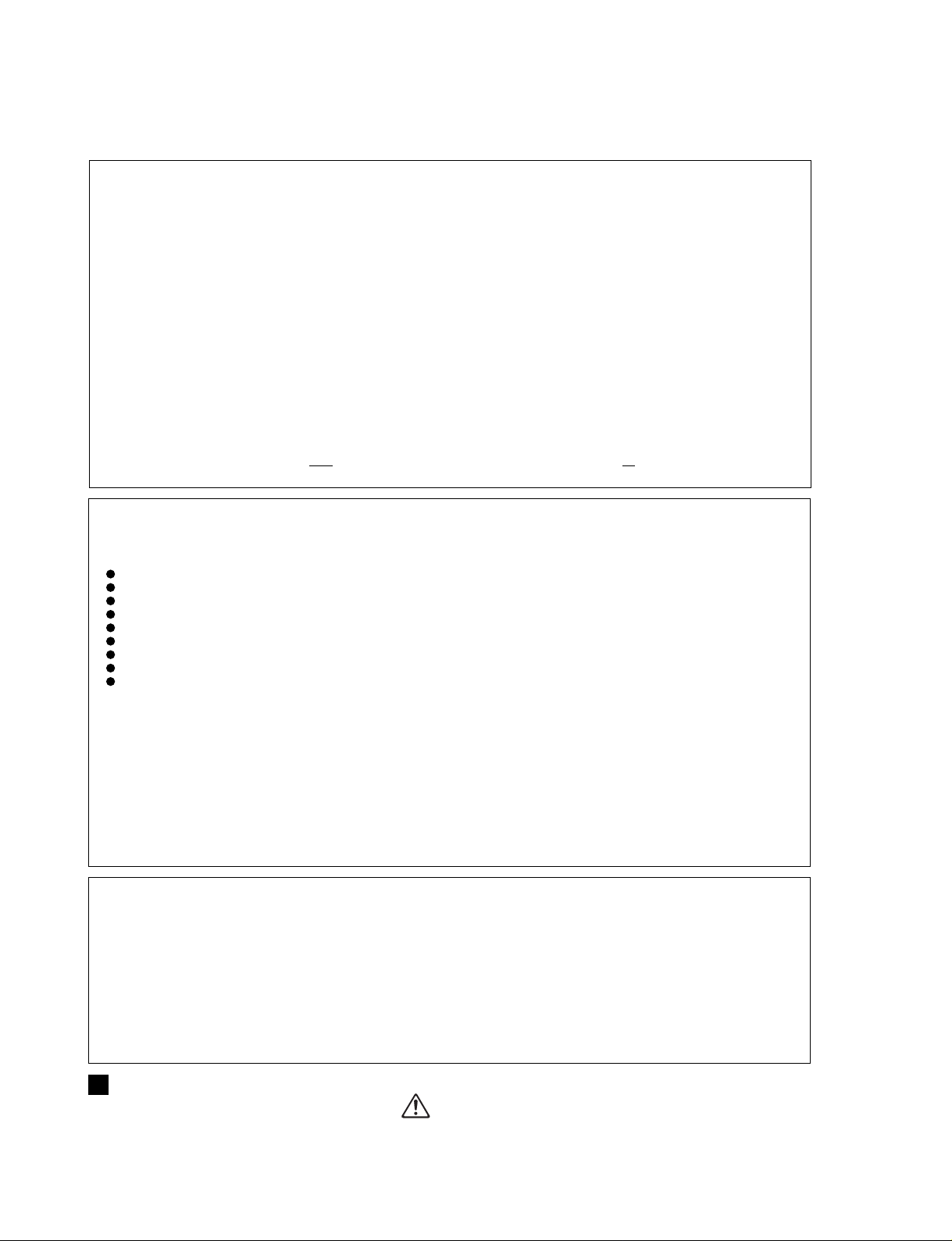
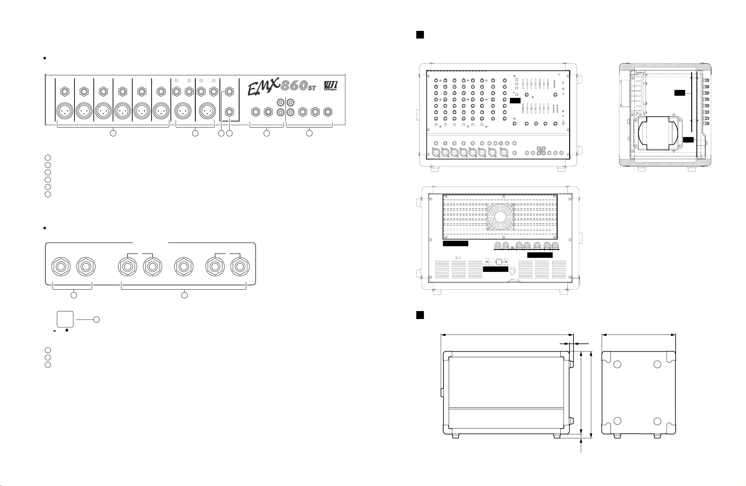
PANEL LAYOUT
Channel section
1
HIGH
–15 +15
MID
1
–15 +15
LOW
–15 +15
MONI
2
3
4
5
010
EFFECT
010
PAN
LR
LEVEL
010
Equalizer controls (HIGH, MID, LOW)
1
Monitor controls (MONI)
2
Effect control (EFFECT)
3
PAN control (BAL/PAN control for CH7/8)
4
Level control (LEVEL)
5
Pad switch (PAD) (1-6 only)
6
EMX860ST
PAD
6
1
DIGITAL EFFECT section
VOCAL
L HALL
S HALL
ON
DIGITAL
EFFECT
EFFECT section
7
8
Effect select switch
7
DIGITAL EFFECT ON switch
8
010
EFFECT OUT
EFFECT
EFFECT OUT control
9
9
5
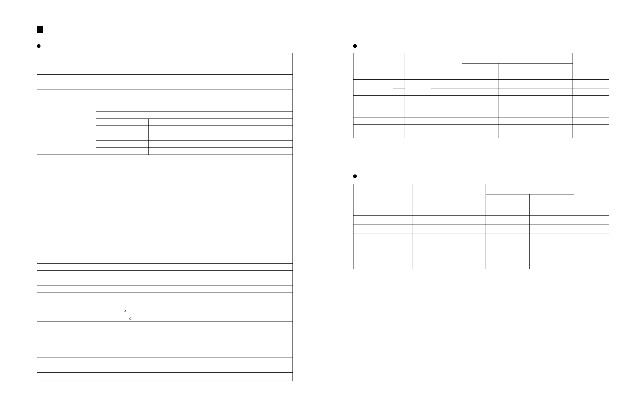
EMX860ST
MONITOR section
10
–12
•
6
•
0
•
6
•
+12
125 250 500 1k 2k 4k 8k
11
010
EFFECT RTN
MONITOR
MAIN section
14
–12
•
6
•
0
•
6
•
+12
125 250 500 1k 2k 4k 8k
–12
+12
•
6
•
0
•
6
•
–12
•
6
•
0
•
6
•
+12
010
MASTER
+6
+3
0
–5
–10
LR
+6
+3
–5
–10
Graphic equalizer
10
EFFECT RTN control
11
MASTER control
12
Peak level indicator
0
13
13
12
Graphic equalizer
14
EFFECT RTN control
15
AUX IN control
16
TAPE IN
19
17
MASTER control
18
Peak level indicator
19
010010
EFFECT RTN AUX IN TAPE IN
MAIN STEREO
15
POWER AMP section
LIMITER
MONI
MAIN
LR
LIMITER
L+R
BRIDGE
16
20
21
STEREO
010
010
MASTER
17
LIMITER indicator
20
Stereo/Bridge select switch
21
18
POWER indicator & PHANTOM switch
22
POWER
PHANTOM
+48V
ON
OFF
23
POWER indicator
22
PHANTOM +48 V switch
23
POWER
AMP
6
30816
H:324
16
W:497 D:275
Unit: mm
MIX
POWER 1/3
POWER 2/3
POWER 3/3
Input/output panel
Hi-Z
Lo-Z
Hi-Z
Lo-Z
Hi-Z
Lo-Z
Hi-Z
Lo-Z
Hi-Z
Lo-Z
1 2
Channel input jacks (Hi-Z, Lo-Z) 1-6
1
Channel input jacks (MIC/LINE) 7-8
2
Effect output jack (EFFECT OUT)
3
Foot switch jack (FOOT SW)
4
AUX IN/TAPE IN jacks
5
REC OUT/MONITOR/MAIN (STEREO) jacks
6
Hi-Z
LR
LINE
(MONO)
MICLo-Z
LINELR
(MONO)
MIC
EFFECT
FOOT SW
3
OUT
EMX860ST
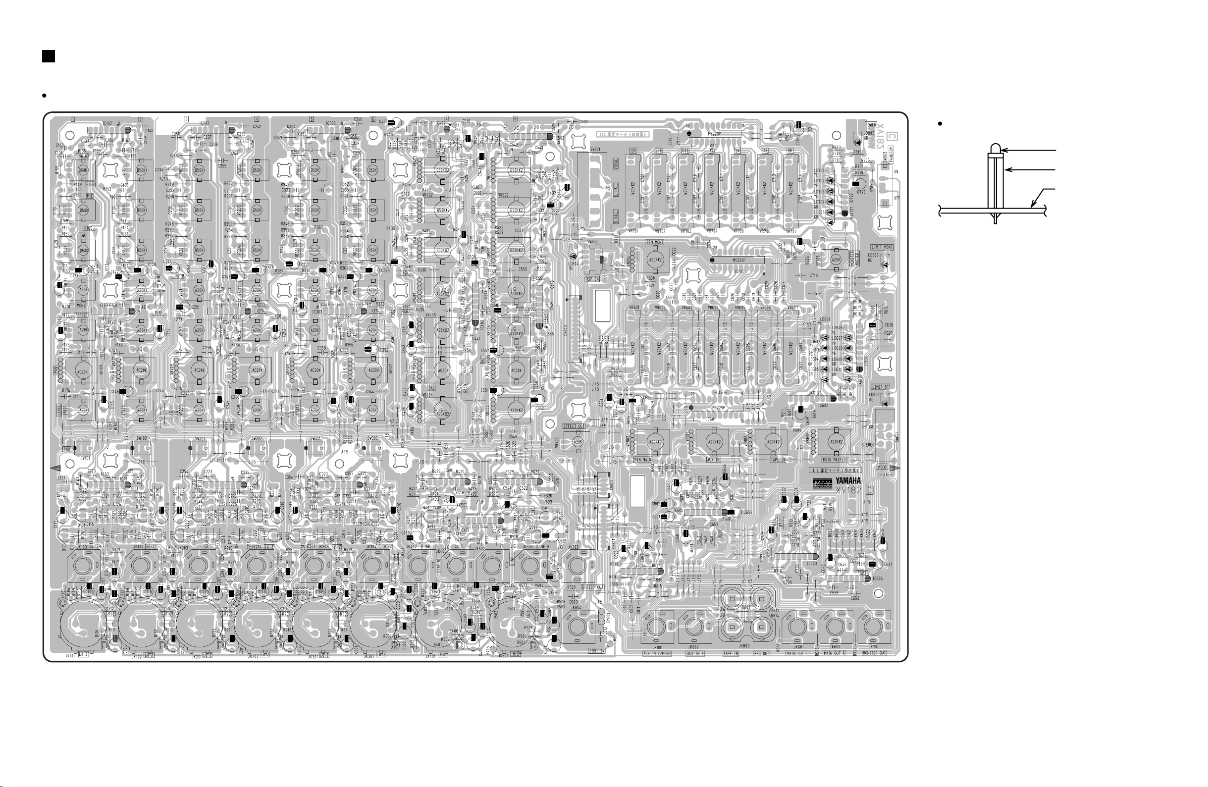
CIRCUIT BOARD LAYOUT
POWERED MIXER
LL
(MONO)
R
RR
INPUT TO MAIN
4
TAPE
IN
5
REC
OUT
MAIN(STEREO) MONITORAUX IN
L
RL
OUTPUT
Power
6
transformer
SUB
MIX
Rear panel
SPEAKERS
MONITOR
A
RL
BRIDGE
1
POWER
3
ON/ OFF
SPEAKERS MONITOR jacks
1
SPEAKERS L/R/L+R BRIDGE jacks
2
Power switch
3
L+R
BABAB
2
DIMENSIONS
(単位)
7
EMX860ST
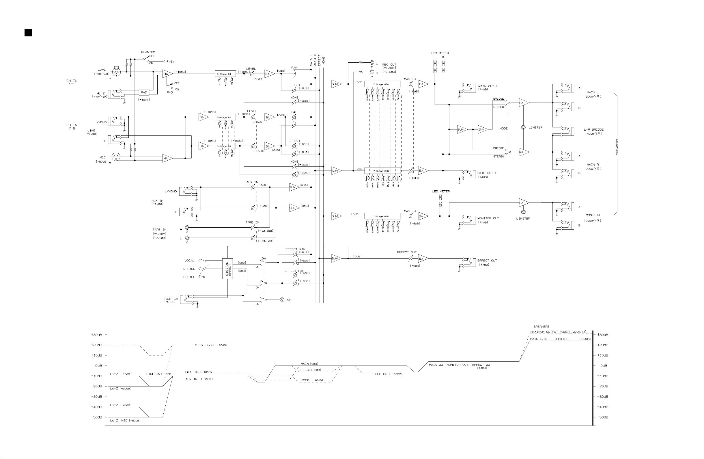
BLOCK & LEVEL DIAGRAM
KEC-92359
8
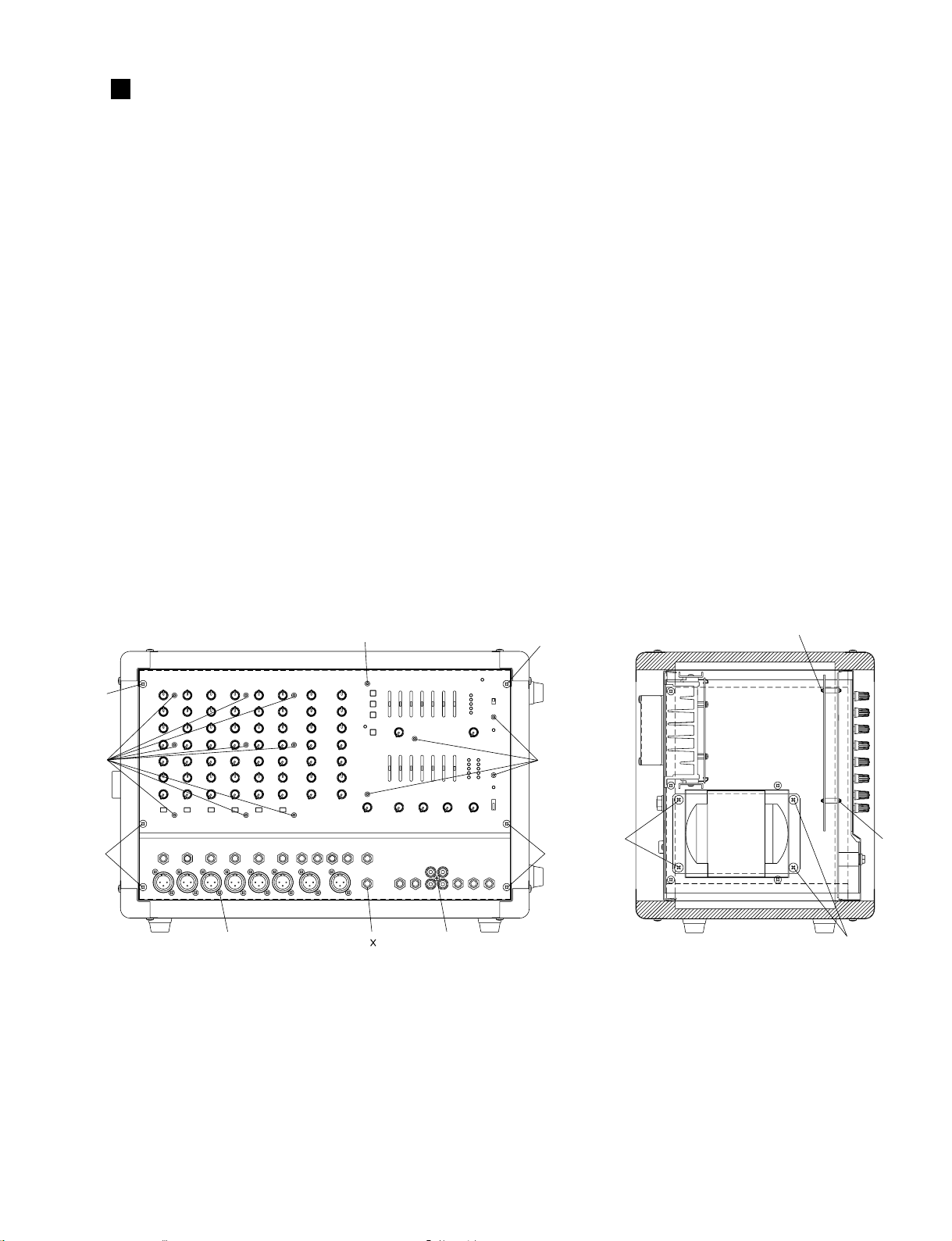
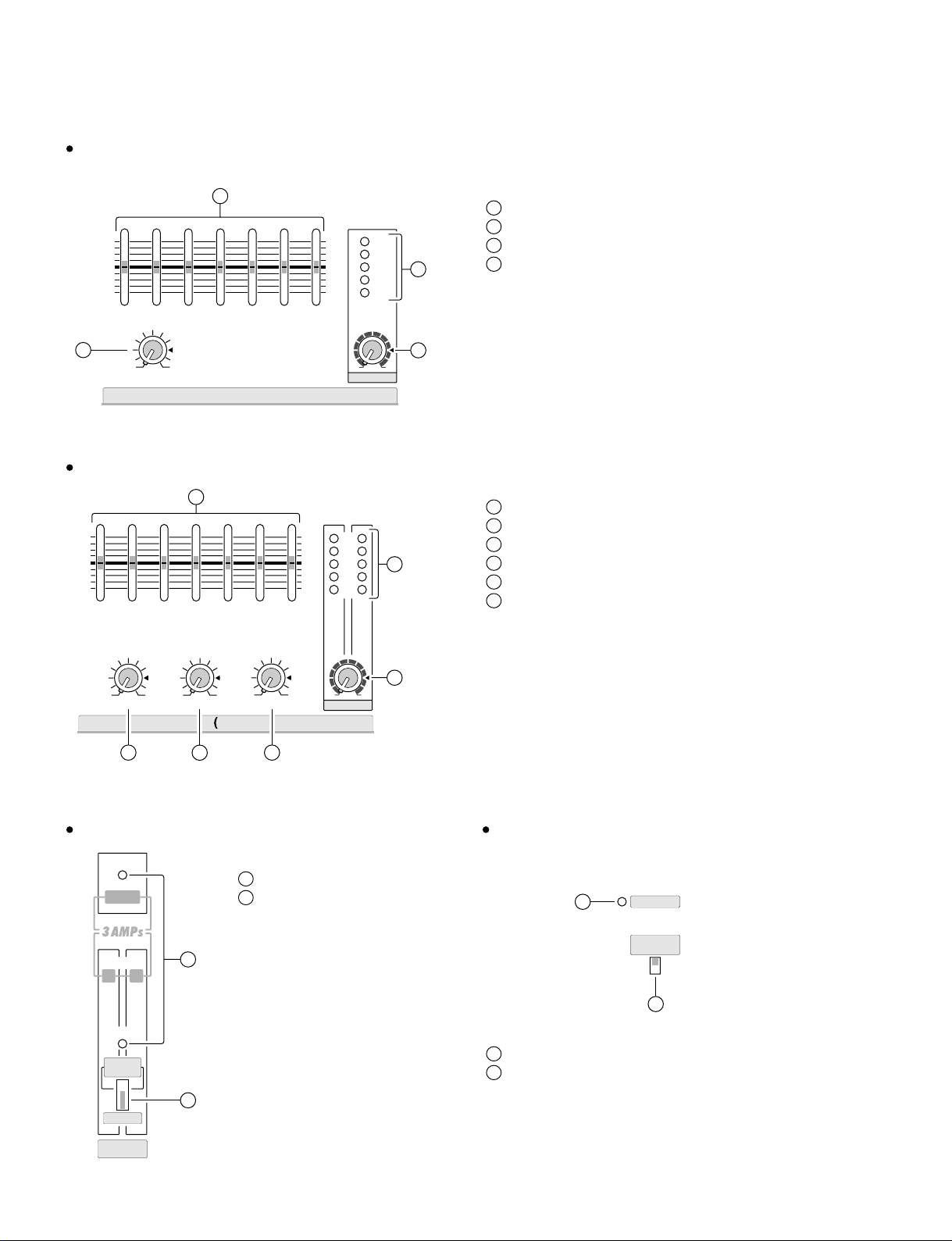
DISASSEMBLY PROCEDURE
1. MIX Circuit Board
1-1 Remove the six (6) screws marked [30]. The panel
assembly can then be removed. (Fig. 1)
1-2 Remove the sixty-three (63) knobs, the seventeen
(17) hexagonal nuts marked [A] and the seventeen
(17) screws marked [P120]. (Fig. 1)
1-3 Remove the fourteen (14) screws marked [P40]. The
MIX circuit board can then be removed. (Fig. 1)
2. SUB Circuit Board
2-1 Remove the panel assembly. (See Procedure 1.)
2-2 Remove the SUB circuit board from the spacer port
marked [P110]. (Fig. 2)
EMX860ST
[P40]
[30]
[P40]
[30]
[P120] [A]
[30]: Bonding B-Tyte Screw 4.0X8 MFZN2BL (VR779900)
[P40]: Hexagonal Socket Screw-P 3X25 MFZNBL (V3289800)
[P120]: Bonding Tapping Screw-P 3.0X8 MFZN2BL (VN413300)
17
Fig.1
[P120]
[P110]
[30]
[P40]
[70]
[30]
[70]: Bind Head Screw SP 5.0X10 MFZN2BL (VU688100)
Fig.2
[P110]
[70]
9

EMX860ST
3. PWR 1/3, 2/3, 3/3 Circuit Boards
3-1 Remove the panel assembly. (See Procedure 1.)
3-2 Remove the two (2) connectors from the power
transformer and the six (6) screws marked [50].
The rear assembly can then be removed. (Fig. 3)
3-3 Remove the six (6) screws marked [R150]. The
radiating plate with the PWR 1/3 circuit board can
then be removed. (Fig. 3)
Remove the fourteen (14) screws marked [R80], the
six (6) screws marked [R40] and the TR holder
marked [R60]. The PWR 1/3 circuit board can then
be removed. (Fig. 4)
3-4 Remove the seven (7) hexagonal nuts marked [B]
and the screw marked [R210A].
The PWR 2/3 circuit board can then be removed.
3-5 Remove two (2) screws marked [R210B]. The PWR
3/3 circuit board can then be removed. (Fig. 3)
4. Motor fan
4-1 Remove the panel assembly. (See Procedure 1-1.)
4-2 Remove the rear assembly. (See Procedure 3-2.)
4-3 Remove the PWS 1/3 circuit board. (See Procedure
3-3.)
4-4 Remove the two (2) screws marked [R100]. The
motor fan can then be removed.
5. Power transformer
5-1 Remove the panel assembly. (See Procedure 1-1.)
5-2 Remove the rear assembly. (See Procedure 3-2.)
5-3 Remove the four (4) screws marked [70]. The power
transformer can then be removed. (Fig. 2)
[R150]
[50]
[R150]
[R100]
[50]
[B]
[R100]
[50]
7
[R210A]
[R60]
[50]
[R40]
[R80]
[R80]
[R40]
[R40]
[R80]
[R80]
[R210B]
[50]: Bonding B-Tyte Screw 4.0X8 MFZN2BL (VR779900)
[R100]: Bind Head Screw 3.0X30 ZMC2BL (VT520200)
[R150]: Bind Head Tapping Screw-B 4.0X8 MFZN2BL (EG340190)
[R210]: Bonding Tapping Screw-B 3.0X8 MFZN2BL (VN413300)
Fig.3
10
[R40]: Bind Head Screw SP 3.0X8 MFZN2Y (EG330290)
[R80]: Bind Head Tapping Screw-B 3.0X12 MFZN2BL (VQ074600)
Fig.4
EMX860ST
NJM2068L-D (XM356A00)
NJM4558L (XM922A00)
Dual Operational Amplifier
BA6137 (XA534A00)
LED Driver
M5229P (XG203A00)
7 SEGMENTS GRAPHIC EQUALIZER
TC74HC14AP (IR001400)
Hex Inverter
TC74HC74AP (IR007400)
Dual D-Type Flip-Flop
D1
+ + + + +
+
Constant
Current
Circuit
1D22D33D44
GND5D56Amp
Output
7IN8
VCC
9
1
2
3
4
5
6
7
8
9
10
11
12
13
14
15
16
17
18
19
20
IN1
IN2
IN3
IN4
IN5
NF1
NF2
NF3
NF4
NF5
-Vcc
GND
+Vcc
OUTPUT
INVERTED
INPUT
NON-INVERTED
INPUT
NF7
NF6
IN7
IN6
-
+
-
+
-
+
-
+
-
+
-
+
-
+
-
+
47k
560
47k
560
47k
560
47k
560
47k
47k
47k
47k
560
10k
10k
11A
2
3
4
5
6
7
1Y
2A
2Y
3A
3Y
GND
8
9
10
11
12
13
14
V
DD
6A
6Y
5A
5Y
4A
4Y
PR CLR
INPUTS OUTPUTS
CK D Q Q
LH H L
HL L H
LL H H
HH t H H L
HH t L H L
HH L Q Q
D
CK
PR
Q
Q
D
CK
PR
Q
Q
CLR
CLR
OO
2PR
11CLR
2
3
4
5
6
7
1D
1CK
1PR
1Q
1Q
GND
8
9
10
11
12
13
14
VCC
2CLR
2D
2CK
2Q
2Q
LSI PIN DISCRIPTION
YSS234 (XN299A00) Digital Sound Processor
PIN
NO.
10 ER1 I Eary refrection preset select 42 MA0 O
11 ER2 I 43 MA1 O
12 REV0 I 44 MA2 O
13 REV1 I Effect select 45 MA3 O
14 REV2 I 46 MA4 O
15 MUTEN I DC D+5V 47 MA5 O External RAM interface address
16 ICN I Initial clear 48 MA6 O
17 PRG I DC D+5V 49 MA7 O
18 MODE I Preset mode (H=DC +5V) 50 MA12 O
19 VSS - Ground 51 MA14 O
20 AVSS - Ground 52 VSS - Ground
21 CVA - N.C. 53 MA10 O
22 AORL O N.C. 54 MA011 O
23 AORR O N.C. 55 MA09 O External RAM interface address
24 CHL I Sample hold capacitor connection 56 MA8 O
25 AIL I Lch ADC input 57 MA13 O
26 VDD - DC D+5V 58 VDD - DC D+5V
27 AIR I Rch ADC input 59 WEN I Write enable
28 CHR I Sample hold capacitor connection 60 OEN I Output enable
29 AOFL O Lch DAC output 61 CEN I Chip select
30 AOFR O Rch DAC output 62 MD7 I/O
31 AVDD - DC A+5V 63 MD6 I/O External RAM interface data
32 CVB I Rch midpoint voltage 64 MD5 I/O
NAME I/O FUNCTION
1 MD4 I/O 33 AVDD - DC A+5Vs bus
2 MD3 I/O 34 VDD - DC D+5V
3 MD0 I/O External RAM interface data 35 TST0 - DC D+5V
4 MD1 I/O 36 TST1 - DC D+5V
5 MD2 I/O 37 DOEN - DC D+5V
6 MCKO O Master clock output 38 SDO1 O N.C.
7 XO O Crystal oscillator connection 39 SDO0 O N.C.
8 XI I Crystal oscillator connection 40 WC O N.C.
9 ER0 I 41 BCO O N.C
PIN
NO.
NAME I/O FUNCTION
IC BLOCK DIAGRAM
11
EMX860ST
LED
LED Spacer
Circuit Board
CIRCUIT BOARDS
MIX Circuit Board
CN803: to SUB-CN101
LED installation
12
Component side
Note : See parts list for details of circuit board component parts.
CN101:
to MIX
-CN803
SUB Circuit Board
EMX860ST
CN301:
to PWR
-CN101
3NA-V295250
CN202:
to MIX
-CN802
CN201:
to MIX
-CN801
Component side
13
EMX860ST
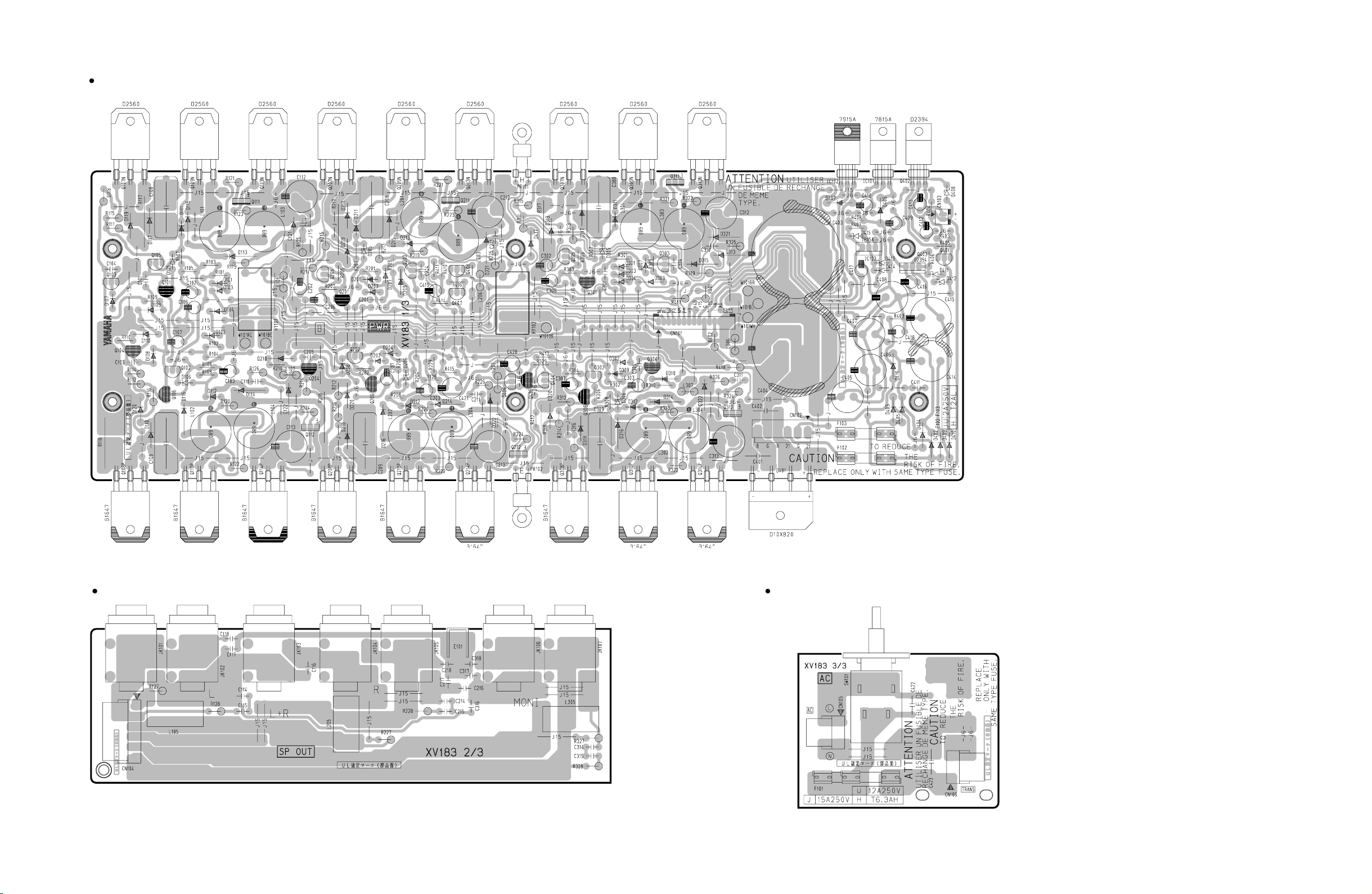
PWR 1/3 Circuit Board
CN101:
to SUB-CN301
PWR 2/3 Circuit Board
Component side
PWR 3/3 Circuit Board
CN105:
to AC
Cable
CN102:
to Transformer
CN106:
to Transformer
14
CN104 : to PWR 1/3 -W101RE-1
-W101BL-2
-W101BE-3
-W101WH-4
-W101OR-5
-W101BR-6
Component side
Component side
KEC-72360

INSPECTIONS
1. Measuring Instruments
Low Frequency Oscillator: Balance Output, Output Impedance = 150 ohms
Oscilloscope: Input Impedance >= 100 kohms
Level Meter: Input Impedance >= 100 kohms
Note: Use a balance input measuring instrument
2. Mixer Part
2-1 Setting Conditions
Setting conditions are as follows unless otherwise specified.
2-2 Input and Output Load
Input Signal: 1 kHz, sine wave (Rs = 150 ohms)
Load: All output terminals have a 10 k ohms load
2-3 Control Panel Setting
Channel Input (CH1-CH6) Section
EQ (HIGH, MID, LOW) level controls: Center
MONITOR level control: Maximum
EFFECT level control: Maximum
PAN: Center
LEVEL: Maximum
PAD: OFF
Stereo Channel Input (CH7-CH8) Section
EQ (HIGH, MID, LOW) level controls: Center
MONITOR level control: Maximum
EFFECT level control: Maximum
PAN: Center
LEVEL: Maximum
EFFECT Section
DIGITAL EFFECT ON switch OFF
EFFECT OUT level control Maximum
MAIN Section
GRAPHIC EQUALIZER (7 band) Fader: Center
EFFECT RTN level control: Maximum
AUX IN: Maximum
TAPE IN: Maximum
MASTER (MAIN): Maximum
MONITOR Section
GRAPHIC EQUALIZER (7 band) Fader: Center
EFFECT RTN level control: Maximum
MASTER (MAIN) level control: Maximum
Others
PHANTOM +48V switch OFF
POWER AMP switch STEREO
EMX860ST
15
EMX860ST
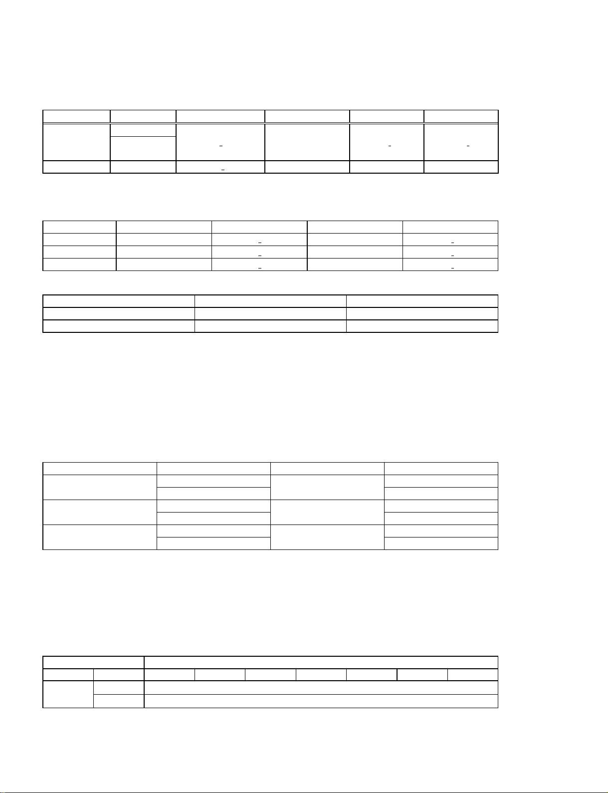
2-4 Gain
Each output gain should be as shown in the table below.
Table 1: INPUT CH 1-CH 6 [Units: dBs]
Input Terminal Input Level M AIN OUT (L, R) MONITOR OUT EFFECT OUT REC OUT (L, R)
Lo-Z -62
-32
+2.5
+1 +4 +10 -16.8
2.0
± 2
+2.5
2.0
(PAD ON)
Hi-Z -52 +1 - - -
+2.5
2.0
Note: When the POWER AMP MODE switch is set to the BRIDGE side, confirm the gain
Table 2: INPUT CH7-CH8 [Units: dBs]
Input Terminal Input Level MAIN OUT MONITOR OUT EFFECT OUT
MIC -62 +1 +7 ± 2+13
LINE L -22 +1 +7 ± 2+13
LINE R -22 +1 +1 ± 2+7
+2.5
2.0
+2.5
2.0
+2.5
2.0
Table 3: AUX IN and TAPE IN [Units: dBs]
Inp u t T e r minal In p ut Level MAIN OUTPUT
AUX IN -22 +4 ± 2
TAPE IN -22 +1.8 ± 2
+2.5
2.0
+2.5
2.0
+2.5
2.0
+2.5
2.0
2-5 Frequency Response
When the input signal frequency is set to 20 Hz and 20 kHz for the systems shown in Tables 1, 2 and 3, the each
output terminal should fall within the range of +1 and -3 dB at 20 Hz and 20 kHz, using 1 kHz as the r eference.
2-6 Equalizer Characteristics
When the input signals shown below are applied to the channel input in the states of 2-3 and the channel EQ (HIGH,MID,
LOW) level controls are changed from center position (flat), the boost/cut range at the MAIN OUT should be as follows:
Table 4 [Units: dB]
EQ Controls GAIN Frequency Response
LOW Maximum 100 Hz +12 ± 2
Minimum +12 ± 2
MID Maximum 2.5 kHz +12 ± 2
Minimum +12 ± 2
HIGH Maximum 10 kHz +12 ± 2
Minimum +12 ± 2
If the result of the equalizer is out of the specified range, change the input signal frequency so that the output
signal is at the set level. Its frequency should then be within the range of 80 - 120% of the standard frequency.
2-7 Graphic Equalizer Characteristics
When the input signals shown below are applied to the channel input in the states of 2-3 and graphic equalizer level controls are
changed from center position (flat), the boost/cut range at the MAIN OUT and the MONITOR OUT should be as follows:
Table 5 [Units: dB]
Input signal frequency and Fader name
125 Hz 250 Hz 500 Hz 1 kHz 2 kHz 4 kHz 8 kHz
Response Maximum
Minimum
+12
±
-12 2
±
2
If the result of the graphic equalizer is out of the specified range, change the input signal frequency so that the
output signal is at the set level. Its frequency should then be within the range of 80 - 120% of the standard
frequency.
16
 Loading...