

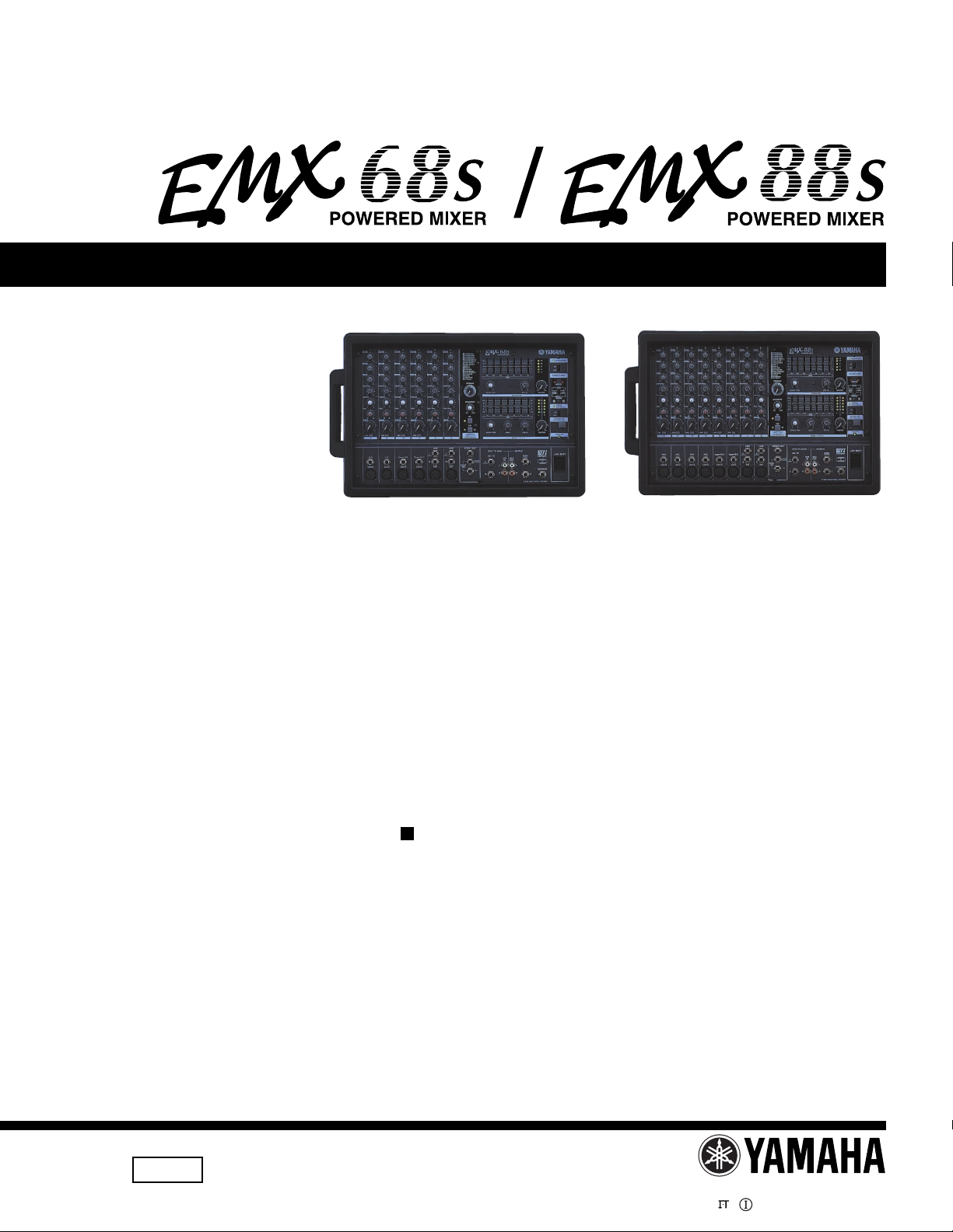
Yamaha EMX-68-S, EMX-88-S Service manual
SERVICE MANUAL
EMX68S EMX88S
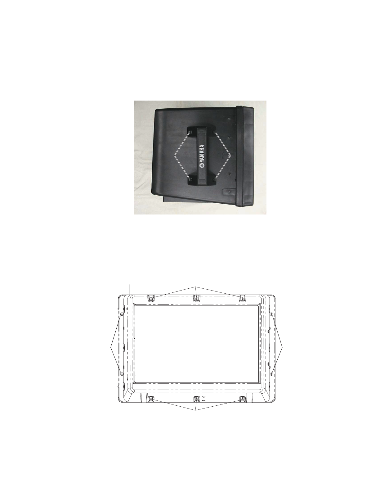
• OPTION
RK-88 RACK MOUNT KIT
This document is printed on chlorine free (ECF) paper with soy ink.
PA 011625
EMX68S 20020325-92000
EMX88S 20020325-105000
RK88 20020325-2500
CONTENTS
SPECIFICATIONS .............................................................................. 3
PANEL LAYOUT.................................................................................. 7
CIRCUIT BOARD LAYOUT & WIRING
.......................................................................................................... 10
DIMENSIONS ....................................................................................11
BLOCK & LEVEL DIAGRAM............................................................. 12
DISASSEMBLY PROCEDURE ......................................................... 14
LSI PIN DESCRIPTION .................................................................... 20
IC BLOCK DIAGRAM........................................................................ 22
CIRCUIT BOARDS ........................................................................... 23
INSPECTION .................................................................................... 37
OVERALL CIRCUIT DIAGRAM
P ARTS LIST
HAMAMATSU, JAPAN
1,387K-7041 Printed in Japan 2002.03
EMX68S / EMX88S
This manual has been provided for the use of authorized Yamaha Retailers and their service personnel. It has been assumed that
basic service procedures inherent to the industry, and more specifically Yamaha Products, are already known and understood by the
users, and have therefore not been restated.
WARNING: Failure to follow appropriate service and safety procedures when servicing this product may result in per-
IMPORTANT: This presentation or sale of this manual to any individual or firm does not constitute authorization, certifica-
The data provided is believed to be accurate and applicable to the unit(s) indicated on the cover. The research engineering, and
service departments of Yamaha are continually striving to improve Yamaha products. Modifications are, therefor, inevitable and
changes in specification are subject to change without notice or obligation to retrofit. Should any discrepancy appear to exist, please
contact the distributor's Service Division.
WARNING: Static discharges can destroy expensive components. Discharge any static electricity your body may have
IMPORTANT: Turn the unit OFF during disassembly and parts replacement. Recheck all work before you apply power to
The solder used in the production of this product contains LEAD. In addition, other electrical / electronic and / or plastic (where
applicable) components may also contain traces of chemicals found by the California Health and Welfare Agency (and possibly other
entities) to cause cancer and / or birth defects or other reproductive harm.
DO NOT PLACE SOLDER, ELECTRICAL / ELECTRONIC OR PLASTIC COMPONENTS IN YOUR MOUTH FOR ANY REASON
WHAT SO EVER!
Avoid prolonged, unprotected contact between solder and your skin! When soldering, do not inhale solder fumes or expose eyes to
solder / flux vapor!
If you come in contact with solder or components located inside the enclosure of this product, wash your hands before handling food.
IMPORTANT NOTICE
sonal injury, destruction of expensive components and failure of the product to per form as specified. For
these reasons, we advise all Yamaha product owners that all service required should be performed by an
authorized Yamaha Retailer or the appointed service representative.
tion, recognition of any applicable technical capabilities, or establish a principal-agent relationship of any
form.
accumulated by grounding yourself to the ground buss in the unit (heavy gauge black wires connect to this
buss).
the unit.
WARNING: CHEMICAL CONTENT NOTICE!
IMPORTANT NOTICE FOR THE UNITED KINGDOM
Connecting the Plug and Cord
WARNING: THIS APPARATUS MUST BE EARTHED
IMPORTANT: The wires in this main lead are coloured in accor-
dance with the following code:
GREEN-AND-YELLOW: EARTH
BLUE: NEUTRAL
BROWN: LIVE
As the colours of the wires in the main lead of this apparatus may not
correspond with the coloured markings identifying the terminals in your
plug, proceed as follows:
The GREEN-and-YELLOW wire must be connected to the terminal in the
plug that is marked with the letter E or the safety earth symbol (or coloured
GREEN or GREEN-and-YELLOW).
The BLUE wire must be connected to the terminal that is marked with the
letter N (or coloured BLACK).
The BROWN wire must be connected to the terminal that is marked with
the letter L (or coloured RED).
This applies only to products distributed by Yamaha Kemble Music (U. K.) Ltd.
WARNING
Components having special characteristics are marked and
must be replaced with parts having specification equal to those
originally installed.
2
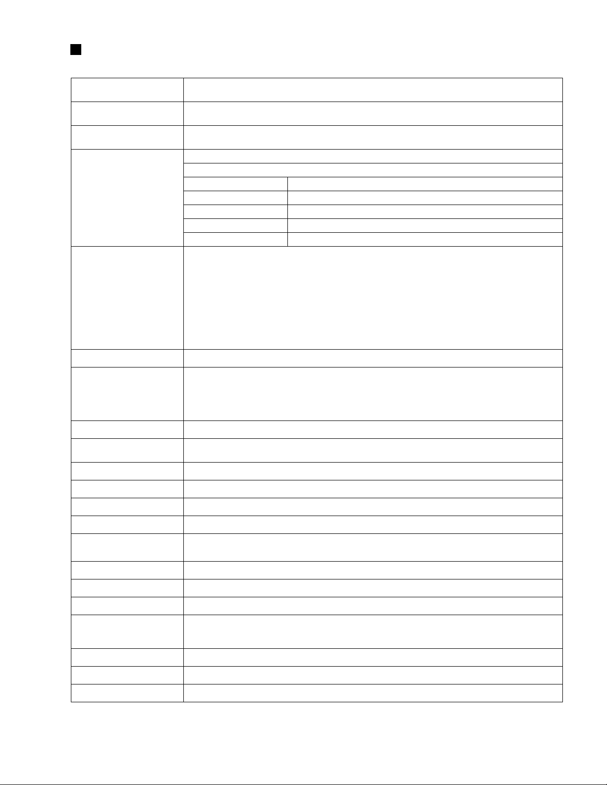
SPECIFICATIONS
● General specifications
Maximum output power
Frequency response
Total harmonic distortion
Hum & noise
(Average, Rs=150Ω)
(with 20 Hz–20 kHz BPF)
Maximum voltage gain
Crosstalk at 1 kHz 65 dB adjacent input, 65 dB input to output
Input channel equalization
Meters 5 POINTS LED METER (MAIN OUT L/R, MONITOR OUT)
Graphic equalizer
Internal digital effect 16 programs, parameter control, tap delay control
MAIN L, R: 400 W+400 W/4Ω @0.5% THD at 1 kHz, 270 W+270 W/8Ω @0.5% THD at 1 kHz
MAIN BRIDGE: 800 W/8Ω @0.5% THD at 1 kHz
20 Hz–20 kHz +1 dB, –3 dB @1 W output into 8Ω (SPEAKERS OUT)
20 Hz–20 kHz +1 dB, –3 dB @+4 dB output into 10 kΩ (MAIN OUT, MONITOR OUT, EFFECT OUT)
Less than 0.5% @20 Hz–20 kHz, 200 W output into 4Ω (SPEAKERS OUT)
Less than 0.3% @20 Hz–20 kHz, +14 dB output into 10 kΩ (MAIN OUT, MONITOR OUT, EFFECT OUT)
–124 dB equivalent input noise, –65 dB residual output noise (SPEAKERS OUT)
–88 dB residual output noise (MAIN OUT, MONITOR OUT)
–79 dB (MAIN OUT) Master level control: nominal level, All channel level controls: minimum
–75 dB (MONITOR OUT) Master level control: nominal level, All channel level controls: minimum
–69 dB (MAIN OUT) Master level control: nominal level, 1 channel level control: nominal level
–84 dB (EFFECT OUT) All channel level controls: minimum
–64 dB (EFFECT OUT) 1 channel level control: nominal level
86 dB CH IN (Lo-Z) to SPEAKERS OUT
66 dB CH IN (Lo-Z) to MAIN OUT, MONITOR OUT
66 dB CH IN (Lo-Z) to EFFECT OUT
48 dB CH IN (Lo-Z) to REC OUT
56 dB CH IN (Hi-Z) to MAIN OUT, MONITOR OUT
46 dB CH IN (Super Hi-Z) to MAIN OUT
26 dB AUX IN to MAIN OUT
24 dB 2TR IN to MAIN OUT
66 dB MIC IN to MAIN OUT
26 dB LINE IN to MAIN OUT
±15 dB Maximum
HIGH 10 kHz shelving
MID 2.5 kHz peaking
LOW 100 Hz shelving
* Turn over/roll-off frequency of shelving: 3 dB below maximum variable level.
7 bands (125, 250, 500, 1k, 2k, 4k, 8k Hz)
±12 dB Maximum (MAIN OUT, MONITOR OUT)
EMX68S / EMX88S
Phantom power +15 V (balanced input)
Limiter Comp. : THD≥0.5% (SPEAKERS OUT)
LIMIT indicators Turns on. : THD≥0.5% (SPEAKERS OUT)
Protection circuit (Power
amp)
Fan circuit stop — low speed (50°C) — variable — high speed (70°C)
Foot switch (FC5) DIGITAL EFFECT MUTE : on/off, Tap delay
Optional accessories RK-88, FC5
Power requirement/
Power consumption
Dimensions (WxHxD) 482 x 305 x 328 mm
Weight 15.5 kg
Supplied accessories AC power cord, Owner’s Manual
POWER switch on/off mute, DC detection, TEMP (heatsink temp. ≥90°C)
USA and Canada 120 V AC 60 Hz/300W
Europe 230 V AC 50 Hz/350W
Other 240 V AC 50 Hz/350W
3
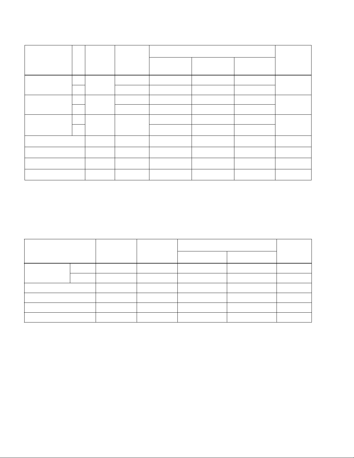
EMX68S / EMX88S
● Input specificaitons
Input connectors PAD
Actual load
impedance
Nominal
impedance
Sensitivity
Input level
Connector
*1
Nominal level
Max. before
clipping
type
CH INPUT (Low-Z)
(CH1–4/1–6)
CH INPUT (Hi-Z)
(CH1–2/1–4)
CH INPUT
(Super Hi-Z)
(CH3–4/5–6)
OFF
3 kΩ
ON 600Ω Lines –32 dB (19.5 mV) –20 dB (77.5 mV) +10 dB (2.45 V)
OFF
10 kΩ
ON 600Ω Lines –22 dB (61.6 mV) –10 dB (245 mV) +20 dB (7.75 V)
OFF
470 kΩ 1kΩ
ON –12 dB (195 mV) 0 dB (775 mV) +10 dB (3.16 V)
50–600Ω Mics –62 dB (0.616 mV) –50 dB (2.45 mV) –20 dB (77.5 mV)
50–600Ω Mics –52 dB (1.95 mV) –40 dB (7.75 mV) –10 dB (245 mV)
–42 dB (6.16 mV) –30 dB (24.5 mV) 0 dB (775 mV)
MIC INPUT 3 kΩ 50–600Ω Mics –62 dB (0.616 mV) –50 dB (2.45 mV) –20 dB (77.5 mV)
LINE INPUT (L, R) 10 kΩ 600Ω Line –22 dB (61.6 mV) –10 dB (245 mV) +20 dB (7.75 V)
AUX IN (L, R) 10 kΩ 600Ω Line –22 dB (61.6 mV) –10 dB (245 mV) +20 dB (7.75 V)
2TR IN (L, R) 10 kΩ 600Ω Line –22 dBV (79.4 mV) –10 dBV (316 mV)
+17.8 dBV (7.76 V)
*1. Sensitivity is the lowest level that can produce an output of +4 dB (1.23 V) or the nominal output level when the unit is set at maximum gain.
(All level controls are at maximum position.)
*2. Balanced.
*3. Unbalanced.
• 0 dB=0.775 Vrms, 0 dBV=1 Vrms.
● Output specificaitons
Output level
Max. before clipping
Output connectors
Actual source
impedance
Nominal
impedance
Nominal
XLR-3-31
*2
type
Phone jack
*2
(TRS)
Phone jack
*3
XLR-3-31 type
Phone jack
Phone jack
Phono jack
*3
*3
Connector
type
*2
SPEAKERS OUT
A, B (1, 2) 0.1Ω 4/8Ω Speaker 80 W/4Ω (400 W/4Ω) Phone jack
BRIDGE 0.1Ω 8Ω Speaker 160 W/8Ω ) Phone jack
(800 W/8Ω
MAIN OUT (L, R) 600Ω 10 kΩ Lines +4 dB (1.23 V) +20 dB (7.75 V) Phone jack
EFFECT OUT 600Ω 10 kΩ Lines +4 dB (1.23 V) +20 dB (7.75 V) Phone jack
MONITOR OUT 600Ω 10 kΩ Lines +4 dB (1.23 V) +20 dB (7.75 V) Phone jack
REC OUT (L, R) 600Ω 10 kΩ Lines –10 dBV (316 mV) +10 dBV (3.16 V) Phono jack
• All output jacks are unbalanced.
• 0 dB=0.775 Vrms, 0 dBV=1 Vrms.
4

EMX68S / EMX88S
5

EMX68S / EMX88S
6
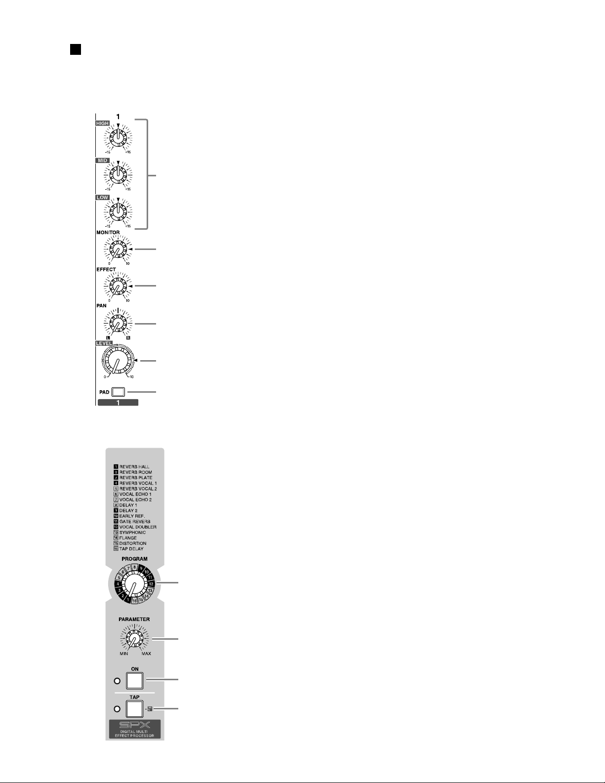
PANEL LAYOUT
● CONTROL P ANEL
1. CONTROL SECTION
• Channel Control
햲
햳
햴
EMX68S / EMX88S
햲 Equalizer (HIGH, MID, LOW)
햳 MONITOR control
햴 EFFECT control
햵 PAN control (EMX-68S/CH1-4, EMX-88S/CH1-6)
BAL/PAN control (EMX-68S/CH5-6, EMX-88S/CH7-8)
햶 LEVEL control
햷 PAD switch (EMX-68S/CH1-4, EMX-88S/CH1-6)
• Digital Effect
햵
햶
햷
햸 PROGRAM selector
햹 PARAMETER control
햺 ON switch
햻 TAP switch
햸
햹
햺
햻
7
EMX68S / EMX88S
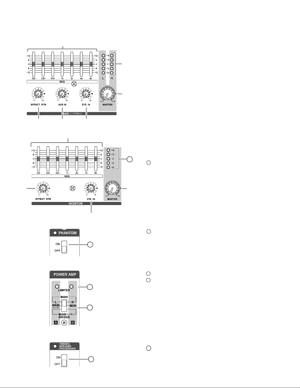
• MAIN
햾햿헀
• MONITOR
햽
헃
헂
헁
21
햽 Graphic Equalizer
햾 EFFECT RTN control
햿 AUX IN control
헀 2TR IN control
헁 MASTER control
헂 Peak Level Indicator
헃 Graphic Equalizer
헄 EFFECT RTN control
헅 2TR IN control
헆 MASTER control
21
Peak Level Indicator
헄
• PHANTOM switch, indicator
• POWER AMP
헅
22
23
24
헆
22
PHANTOM ON/OFF switch
23
LIMITER indicator
24
Power Amp select switch
• YAMAHA SPEAKER PROCESSING
8
25
25
ON/OFF switch
• STAND-BY • POWER switch, indicator
27
POWER ON/OFF switch,
indicator
27
26
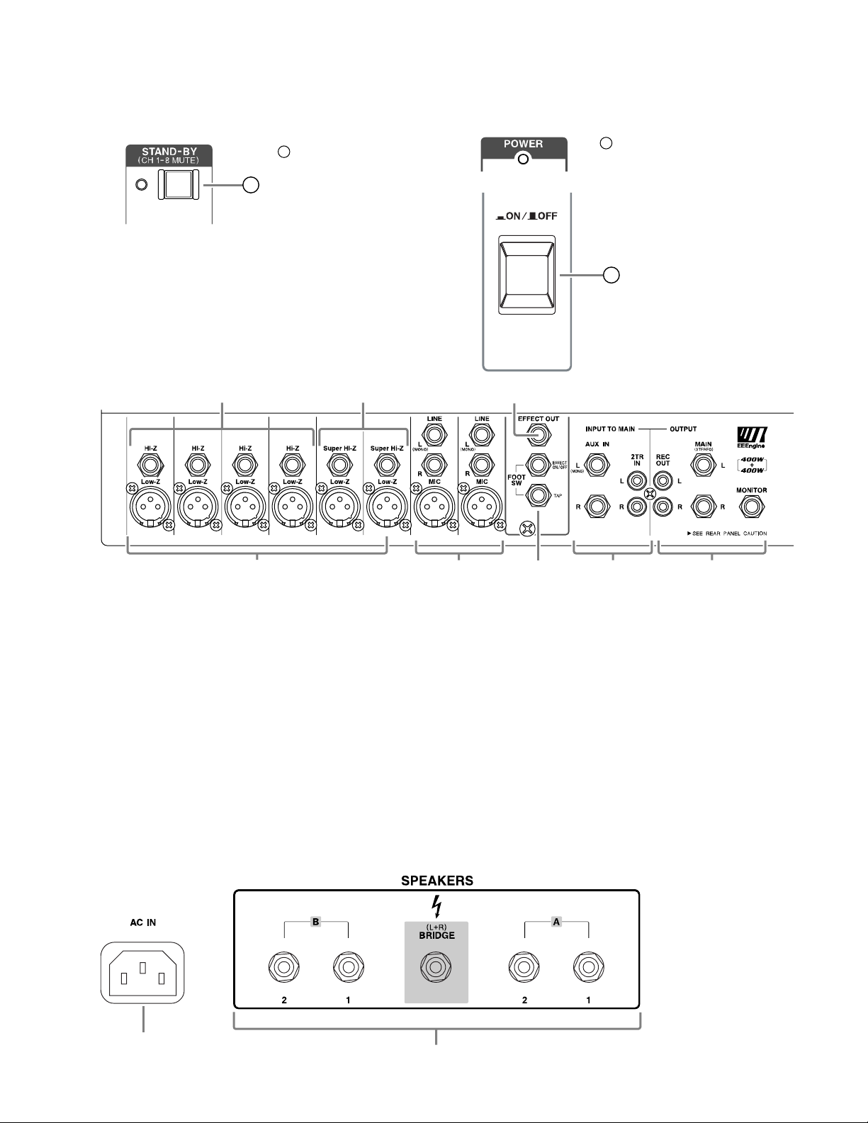
2. INPUT/OUTPUT SECTION
26
ON/OFF switch
햳햴 햶
EMX68S / EMX88S
햲 INPUT terminal (Low-Z)
(EMX-68S/CH1-4, EMX-88S/CH1-6)
햳 INPUT terminal (Hi-Z)
(EMX-68S/CH1-2, EMX-88S/CH1-4)
햴 INPUT terminal (Super Hi-Z)
(EMX-68S/CH3-4, EMX-88S/CH5-6)
햵 INPUT terminal (MIC, LINE)
(EMX-68S/CH5-6, EMX-88S/CH7-8)
햶 EFFECT OUT terminal
햷 FOOT SW terminal
햸 INPUT TO MAIN terminal (AUX IN, 2TR IN)
햹 OUTPUT terminal (REC OUT, MAIN(STEREO),
MONITOR)
● REAR P ANEL
햵햷햸 햹햲
햲 SPEAKERS terminal
햳 AC IN socket
햳
햲
9
EMX68S / EMX88S
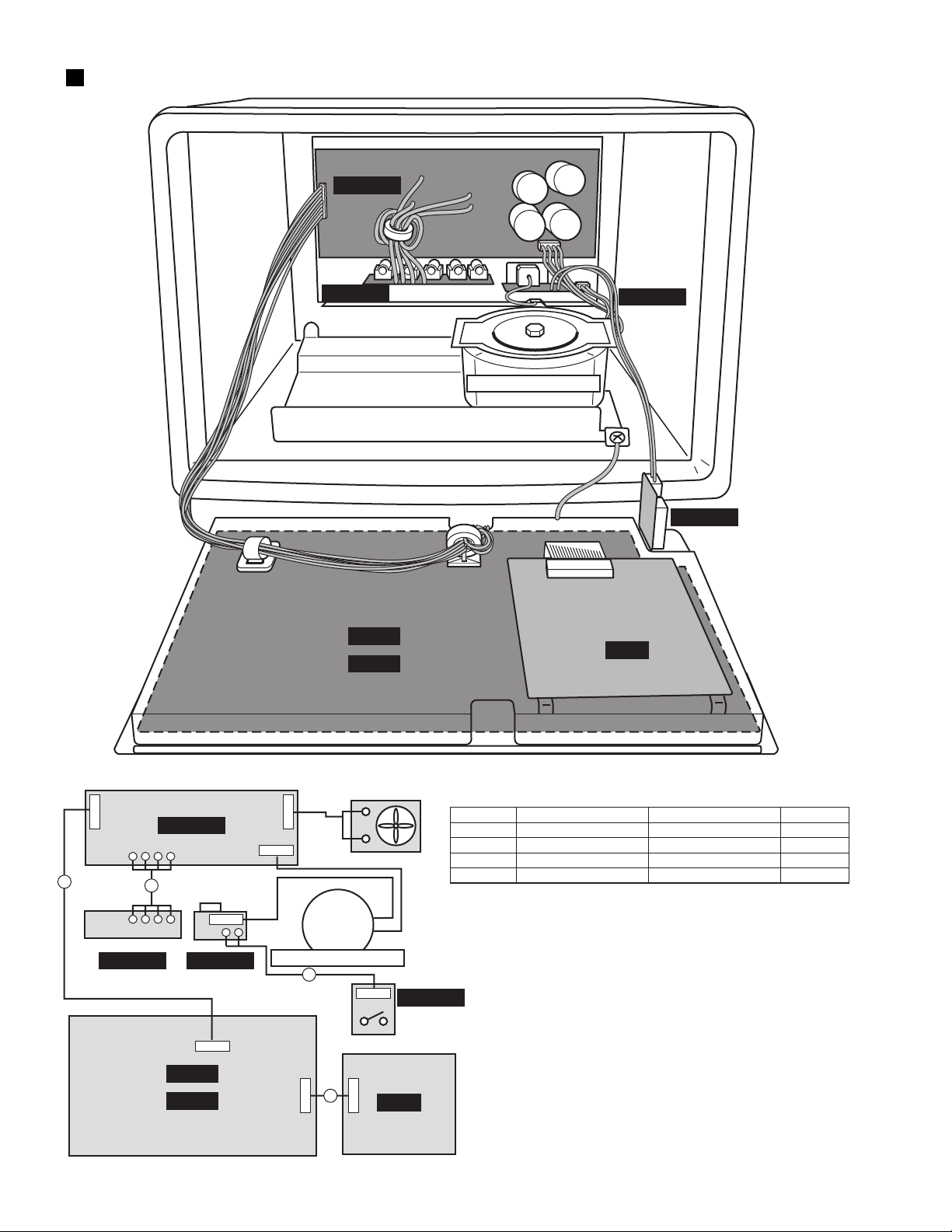
CIRCUIT BOARD LAYOUT & WIRING
PWR 1/4
PWR 2/4
MIX88
MIX68
PWR 3/4
Power T ransformer
PWR 4/4
DSP
10
15P
1
CN101
PWR 2/4
PWR 1/4
3
MIX88
MIX68
AC INLET
CN104
PWR 3/4
15P
CN903
2P
CN105
CN106
6P
3P
Power T ransformer
4
27P 27P
2
CN901
DC Fan
CN107
CN101
3P
PWR 4/4
POWER
ON/OFF
DSP
Location Connector Assembly Remarks Parts No.
1 MIX68/88-PWR1/4
2 MIX68/88-DSP 100mm P=1.25 MF12710
3 PWR1/4-PWR2/4 B&B4P (V827270)
4 PWR3/4-PWR4/4 PSW V827290
24185&2426 15P L=700
V842620
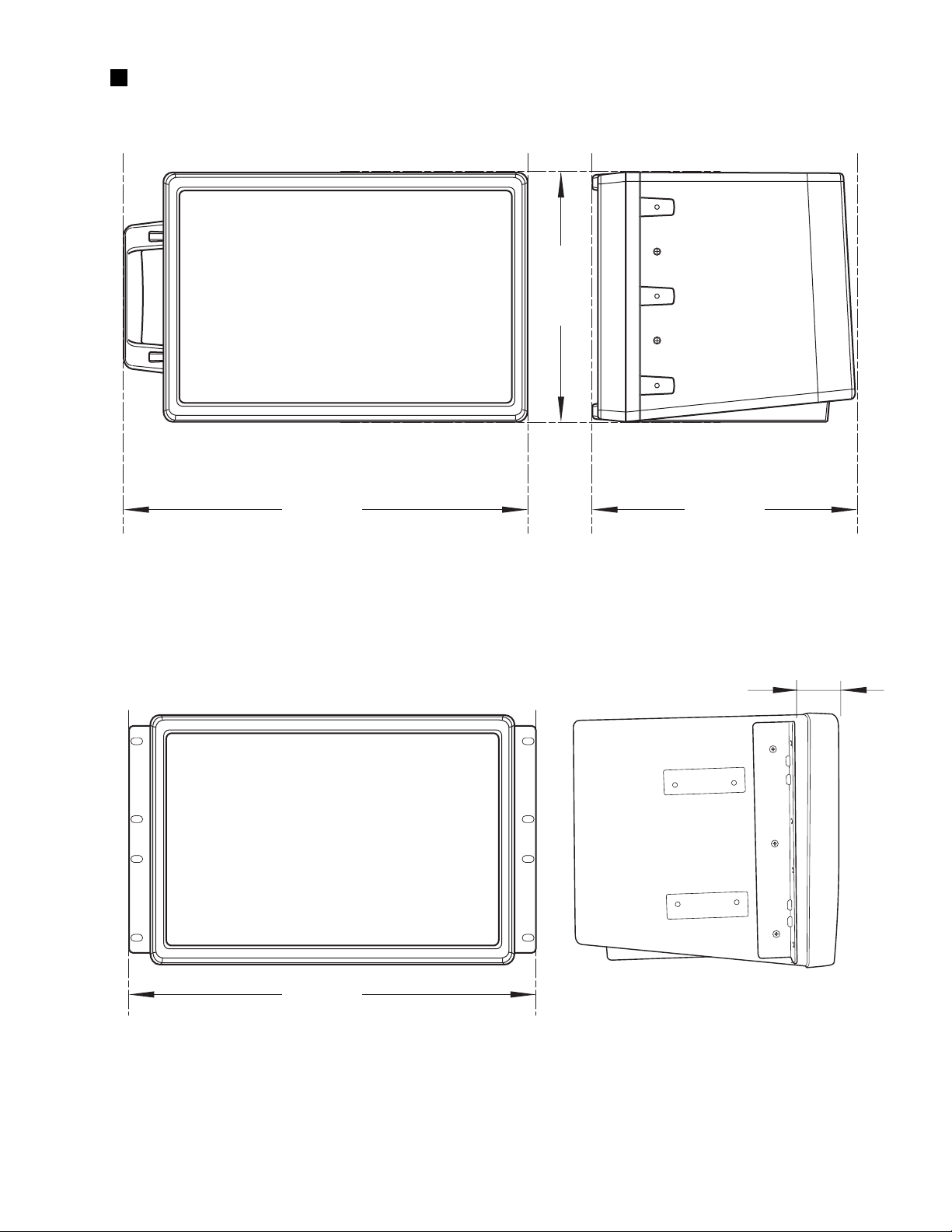
DIMENSIONS
● Front View ● Side View
305mm
EMX68S / EMX88S
481.5mm
● Front View with Rack Mount Adaptor
327.6mm
62mm
448.5mm
11
EMX68S / EMX88S
C
M
M
M
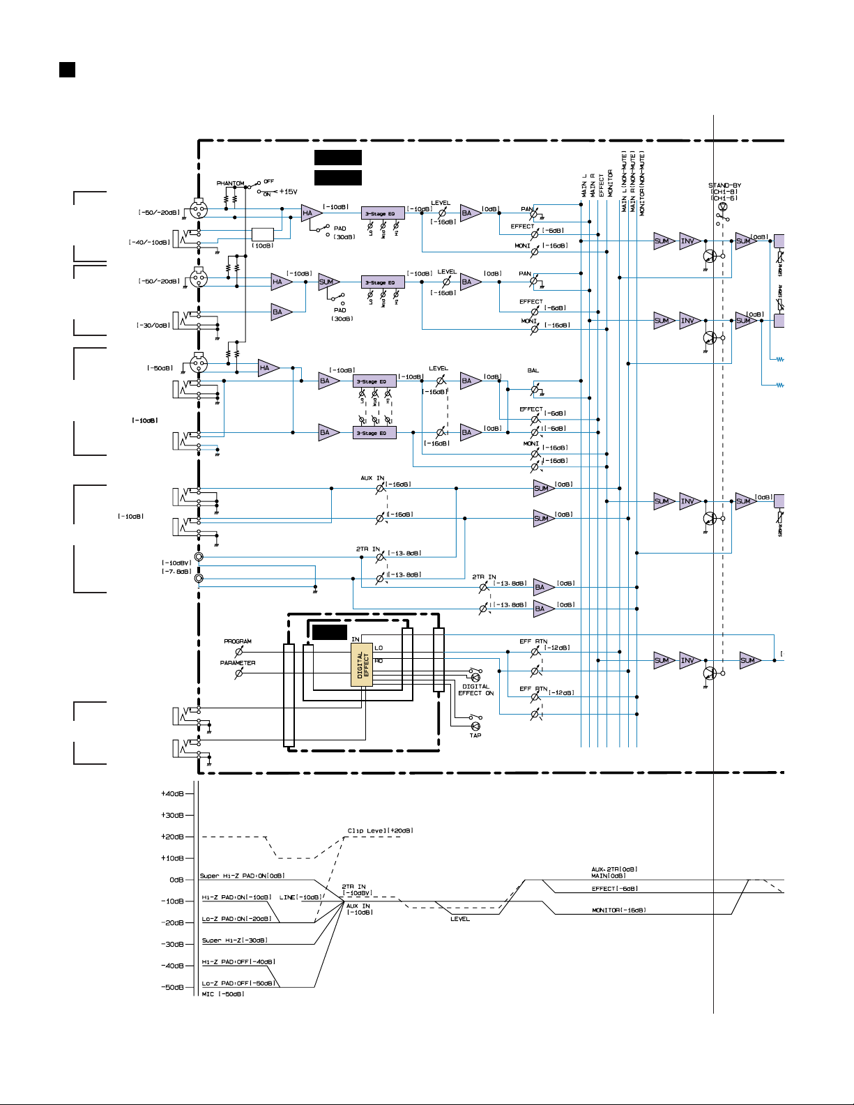
BLOCK & LEVEL DIAGRAM
A
CH INPUT
EMX-68S [CH1,2]
EMX-88S [CH1-4]
CH INPUT
EMX-68S [CH3,4]
EMX-88S [CH5,6]
CH INPUT
EMX-68S [CH5,6]
EMX-88S [CH7,8]
INPUT TO MAIN
FOOT SW
Super Hi-Z
L/MONO
LINE
L/MONO
AUX IN
2TR IN
EFFECT
ON/OFF
TAP
Low-Z
Hi-Z
Low-Z
MIC
R
R
12
3
2
4
3
1
12
3
2
4
3
1
12
3
2
4
3
1
2
4
3
1
2
4
3
1
2
4
3
1
L
R
EMX-68S/88S:EN901
EMX-68S/88S:VR905
2
4
3
1
2
4
3
1
EMX-68S/88S:
SW906
EMX-68S/88S:
IC502
6
5
57
EMX-68S/88S:IC501
EMX-68S/88S:IC704
6
5
7
21-24 12-15
20 16
CN901-27PIN
13 23 22
14
MIX68
MIX88
EMX-68S:IC101
EMX-88S:IC101,301
6
5
7
EMX-68S/88S:
IC503
5
7
EMX-68S/88S:
IC701,801
57
EMX-68S/88S:
IC701,801
31
DSP
EMX-68S/88S:
IC102
EMX-68S/88S:
IC504
7
EMX-68S/88S:
IC702,802
EMX-68S/88S:
IC702,802
CN101-27PIN
18,19
20,21
EMX-68S:IC103
EMX-88S:IC103,303
57
EMX-68S/88S:IC505
57
EMX-68S/88S:IC703,803
57
31
EMX-68S/88S:IC703,803
829
CN901-27PIN
928
1027
EMX-68S/88S:IC901
EMX-68S/88S:IC901
EMX-68S/88S:IC902
EMX-68S/88S:IC902
21
67
21
57
216
EMX-68S/88S:
IC920
216
EMX-68S/88S:
IC921
216
EMX-68S/88S:
IC922
216
EMX-68S/88S:
IC923
EMX-68S/88S:
IC920
EMX-68S/88S:
IC921
EMX-68S/88S:
IC922
EMX-68S/88S:
IC923
7
7
7
7
EMX-68S/88S:
IC903
6
7
EMX-68S/88S:
IC903
2
1
EMX-68S/88S:
IC904
6
7
2
EMX-68S/88S:I
E
E
E
1
12
A’
EMX-68S/88S:
IC920
216
X-68S/88S:
920
EMX-68S/88S:
IC921
216
X-68S/88S:
921
EMX-68S/88S:
IC922
216
MX-68S/88S:
922
EMX68S / EMX88S
A
EMX-68S/88S:IC911
8
1,2,3,4,7
EMX-68S/88S:IC912
8
EMX-68S/88S:
IC903
6
7
EMX-68S/88S:IC905,906
7
EMX-68S/88S:IC914
5
7
1,2,3,4,7
2
MAIN L
4
3
1
PWR 2/4
SPEAKERS
PWR 1/4
1
A
2
BRIDGE
1
B
2
2
4
3
1
2
MAIN R
4
3
1
EMX-68S/88S:IC917,918
EMX-68S/88S:
IC917,918
EMX-68S/88S:SW905
MONITOR
CN903-15PIN
CN101-15PIN
PA
PA
W101RE1
W101BE1
W101RE2
+
W101BE2
+++
EMX-68S/88S:
IC903
2
7
1
EMX-68S/88S:IC907,908
REC OUT
EMX-68S/88S:
IC904
6
7
EMX-68S/88S:IC909,910
7
3
EMX-68S/88S:IC914
1
5
7
EMX-68S/88S:IC916
EMX-68S/88S:IC915
3
5
7
EMX-68S/88S:IC915
1
EMX-68S/88S:SW904
216
MX-68S/88S:
923
EMX-68S/88S:
IC923
2
7
1
EMX-68S/88S:IC904 EMX-68S/88S:IC916
EMX-68S/88S:IC913
8
1,2,3,4,7
3
1
2
4
3
1
EFFECT OUT
A’
38CA1-8822109 1
13
EMX68S / EMX88S
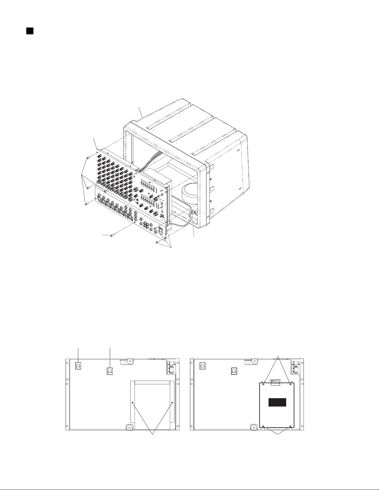
DISASSEMBLY PROCEDURE
1. Front Panel Assembly (Time required: about 3 min)
1-1. Remove the seven (7) screws marked [80] and the
screw marked [90]. (Fig.1)
1-2. Hold volume knobs and pull the front panel
forward. (Fig.1)
1-3. Remove the screw marked [100]. The front panel
assembly can then be removed. (Fig.1)
Front Panel Assembly
[80]
Body Assembly
[90]
[80]: Bind Head Screw 4.0X12 MFZN2BL (VB132700)
[90]: Bind Head Screw 4.0X20 MFZN2BL (VB403600)
[100]: Bind Head Screw A4.0X8 MFZN2BL (VP156800)
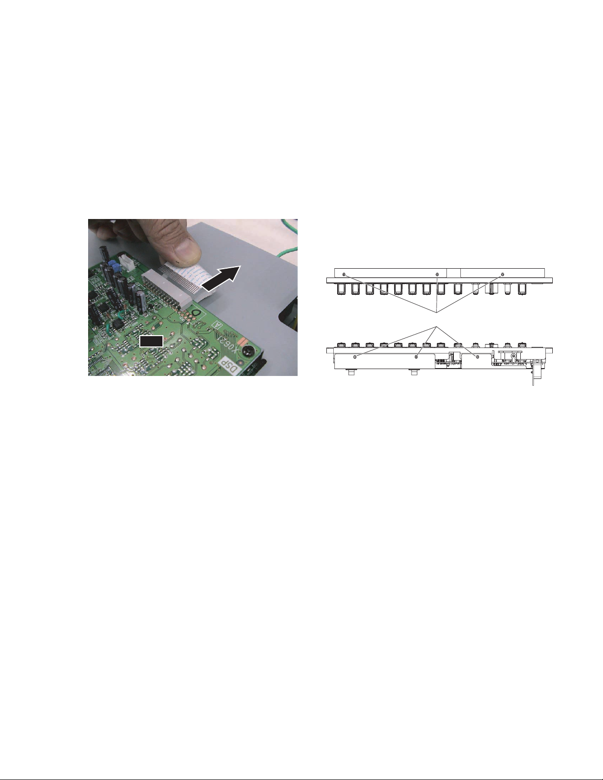
2. DSP-SPX1 Circuit Board (Time required: about 4 min)
2-1. Remove the front panel assembly. (See Procedure 1)
2-2. Remove the two (2) screws marked [170] to
remove the shield case. (Fig.2)
2-3. Remove the four (4) screws marked [140]. The
DSP-SPX1 circuit board can then be removed.
(Fig.2)
[250]
[270]
[80]
[100]
(Fig. 1)
[140]
DSP
14
[170] [140]
[140]: Bind Head Tapping Screw-B 3.0X6 MFZN2BL (EP600230)
[170]: Bind Head Tapping Screw-B 3.0X6 MFZN2BL (EP600230)
[250]: Cord Binder TS-0708 KSS (VZ765100)
[270]: Cable Cramp AB-3S-3M NYLON66 (V9078900)
(Fig. 2)
3. MIX68 Circuit Board (EMX68S)
(Time required: about 18 min)
MIX88 Circuit Board (EMX88S)
(Time required: about 20 min)
3-1. Remove the front panel assembly. (See Procedure 1)
3-2. Remove the cable from the cord binder marked
[250]. (Fig.2)
3-3. Remove the shield case. (See Procedure 2-2)
3-4. Pull out the connector assembly from CN101 on
the DSP-SPX1 circuit board. (Fig.4)
3-5. Remove the six (6) screws marked [240] to remove
the shield plate. (Fig.3)
EMX68S / EMX88S
PullPull
DSP
(Fig. 4)
3-6. EMX68S: Remove the fifteen (15) screws marked
[40], and the thirteen (13) screws
marked [41], and the sixteen (16)
hexagonal nuts marked [A]. (Fig.5)
EMX88S: Remove the fifteen (15) screws marked
[40], and the seventeen (17) screws
marked [41], and the eighteen (18)
hexagonal nuts marked [A]. (Fig.5)
3-7. EMX68S: Remove the eighteen (18) knobs marked
[50], the nine (9) knobs marked [60], the
nine (9) knobs marked [70], six (6)
knobs marked [80], and the nine (9)
knobs marked [90]. The mix68 circuit
board can then be removed. (Fig.5)
EMX88S: Remove the twenty-four (24) knobs
marked [50], the eleven (11) knobs
marked [60], the eleven (11) knobs
marked [70], eight (8) knobs marked
[80], and the eleven (11) knobs marked
[90]. The mix88 circuit board can then
be removed. (Fig.5)
T op Vie w
[240]
Bottom View
[240]: Bind Head Tapping Screw-B 3.0X6 MFZN2BL (EP600230)
(Fig. 3)
Note: When placing the front panel assembly on
the table, take care not to weight the PWR
circuit board 4/4. (Fig.6)
15
EMX68S / EMX88S
[120]
[60] [70] [90][90]
[40] [40] [40] [40] [40] [40] [40] [40] [40][40]
EMX88SEMX68S
[50]
[60] [70] [90][90][50]
[70]
[60]
[80]
[90]
[A] [A][41] [A] [A][41][41] [41]
[40]: Screw X25 MFZNBL (V3289800)
[41]: Bonding Tapping Screw-B 3.0X8 MFZN2BL (VN413300)
[50]: Knob GREEN/M-GRAY (V6225300)
[60]: Knob L-GRAY/M-GRAY (V6225600)
[70]: Knob BLUE/M-GRAY (V6225400)
[80]: Knob RED/M-GRAY (V6225500)
[90]: Knob L-GRAY/D-GRAY (V6225700)
[70]
[60]
[80]
[90]
(Fig. 5)
4. PWR Circuit Board 4/4 (Time required: about 4 min)
4-1. Remove the front panel assembly. (See Procedure 1)
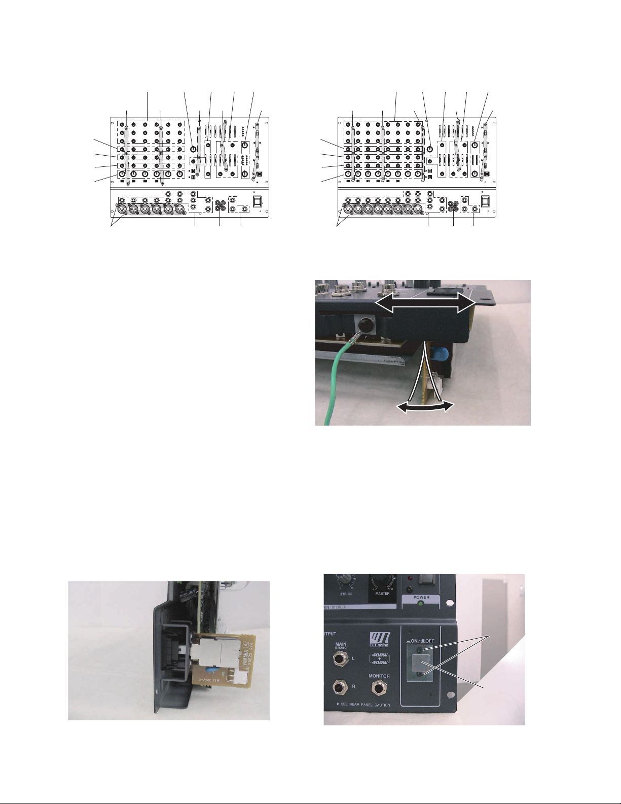
4-2. Pinch slightly the stopper of the power switch
escutcheon with a plyer, pull it to the front to
remove. (Fig.7-1)
4-3. Remove the two (2) screws marked [100]. (Fig.7-2)
4-4. Remove the power switch knob marked [120]. The
PWR circuit board 4/4 can then be removed.
(Fig.7-2)
(Fig. 7-1)
16
(Fig. 6)
[100][100]
[120]
(Fig. 7-2)
[100]: Bind Head Screw 3.0X8 MFZN2BL (VB659000)
[120]: Power Switch Knob MX12/4 (VU859000)
5. Rear Panel Assembly
(Time required: about 5 min)
5-1. Remove the front panel assembly. (See Procedure 1)
5-2. Remove the eight (8) screws marked [60] and the
two (2) screws marked [44]. (Fig.8)
5-3. Hold the cord holder and pull the rear panel
forward to remove. (Fig.9)
[60]
[130]
[C]
EMX68S / EMX88S
[140][150b]
[150a]
[60][44]
[44]
(Fig. 8)
[44]: Bind Head Tapping Screw-B 4.0X8 MFZN2BL (EG340190)
[60]: Bind Head Screw 4.0X12 MFZN2BL (VB132700)
[130]: Bind Head Screw 4.0X30 MFZN2BL (VT229100)
[140]: Bind Head Tapping Screw-B 3.0X12 MFZN2BL (VQ074600)
[150]: Bonding Tapping Screw-B 3.0X8 MFZN2BL (VN413300)
Note: When reinstalling, install the rear panel
assembly and the front panel assembly in that
order to connect the PSW connector easily.
6. PWR Circuit Board 2/4
(Time required: about 7 min)
6-1. Remove the rear panel assembly. (See Procedure 5)
6-2. Remove the screw marked [150a] and the five (5)
hexagonal nuts marked [C]. The PWR circuit board
2/4 can then be removed. (Fig.8)
7. PWR Circuit Board 3/4
(Time required: about 6 min)
7-1. Remove the rear panel assembly. (See Procedure 5)
7-2. Remove the two (2) screws marked [140] and the
screw marked [150b]. (Fig.8)
7-3. Remove the screw marked [240]. The PWR circuit
board 3/4 can then be removed. (Fig.10)
(Fig. 9)
Rear Panel Assembly
[240]
(Fig. 10)
[240]: Bind Head Screw A4.0X8 MFZN2BL (VP156800)
17
EMX68S / EMX88S
[90]
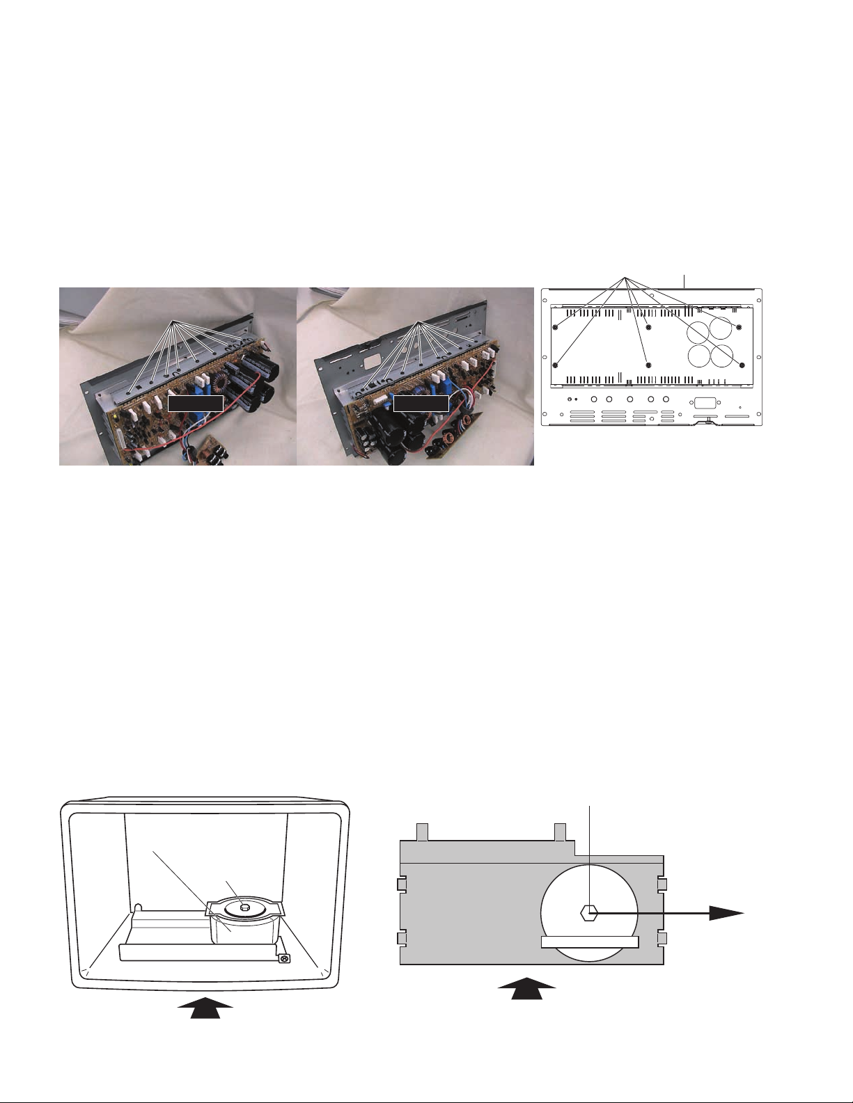
8. PWR Circuit Board 1/4 (Time required: about 13 min)
8-1. Remove the rear panel assembly. (See Procedure 5)
8-2. Remove the PWR circuit board 2/4. (See Procedure 6)
8-3. Remove the PWR circuit board 3/4. (See Procedure 7)
8-4. Remove the sixteen (16) screws marked [90] to
remove the TR holder A and the TR holder B.
(Fig.11)
8-5. Remove the six (6) screws marked [40]. The PWR
circuit board 1/4 can then be removed. (Fig.12)
Upper Side View Bottom Side View
[40] Rear Panel
[90][90] [90]
PWR 1/4 PWR 1/4
(Fig. 11)
[90]: Bind Head Tapping Screw-B 3.0X12 MFZN2BL (VQ074600)
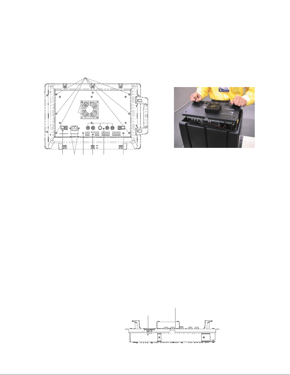
9. Fan (Time required: about 6 min)
9-1. Remove the rear panel assembly. (See Procedure 5)
9-2. Remove the two (2) screws marked [130]. The fan
can then be removed. (Fig.8)
10.
Power Transformer (Time required: about 4 min)
10-1. Remove the front panel assembly. (See Procedure 1)
10-2. Remove the bolt marked [D]. The power trans-
former can then be removed. (Fig.13)
Note: When reinstalling the power transformer,
make sure to lead the cables to the direction
shown in Fig.14. Leading them to unfit
direction may cause hum noise on the
system.
[90]
(Fig. 12)
[40]: Bind Head Screw SP 3.0X8 MFZN2Y
(EG330290)
18
Power T ransformer
[D]
FRONT VIEW
(Fig. 13) (Fig. 14)
Direction to lead
the cables
Power Transformer
FRONT VIEW
Body Assemb
Handle
11. Front Frame (Time required: about 6 min)
11-1. Remove the front panel assembly. (See Procedure 1)
11-2. Remove the four (4) screws marked [50] to remove
the handle assembly. (Fig.15)
11-3. Remove the ten (10) screws marked [40]. The front
frame can then be removed. (Fig.16)
EMX68S / EMX88S
Body Assemb
Body Assembly
[50] [50]
[50] [50]
ly
Handle
Handle
(Fig. 15)
[50]: Bind Head Screw 4.0X16 MFZN2BL (EG340110)
Body Assembly
[40]
[40][40]
[40]
(Fig. 16)
[40]: Bind Head Tapping Screw-P 4.0X30 MFZN2BL (V8322700)
19
EMX68S / EMX88S
LSI PIN DESCRIPTION
● M30622MCA-XXXFP (X2416A00) CPU DSP: IC109
PIN PIN
NAME I/O FUNCTION
NO.
1 P96/ I/O 41 P55/HOLD I/O CMOS 8Bit Input Output Port
2 P95/ I/O 42 P54/HLDA I/O CMOS 8Bit Input Output Port
3 P94/ I/O 43 P53/BCLK I/O CMOS 8Bit Input Output Port
4 P93/ I/O CMOS 8Bit Input Output Port 44 P52/RD I/O CMOS 8Bit Input Output Port
5 P92/ I/O 45
6 P91/ I/O 46
7 P90/ I/O 47 P47/CS3 I/O
8 BYTE I BASS change Terminal 48 P46/CS2 I/O
9 CN Vss I Change Processor Mode 49 P45/ CS1 I/O
10
P87/X CIN
11
P86/X COUT
12 RESET I Reset Input 52 P42/A18 I/O
13 X OUT O Main Clock Output 53 P41/A17 I/O
14 Vss Ground 54 P40/A16 I/O
15 X IN I Main Clock Input 55 P37/A15 I/O
16 Vcc Power Supply 56 P36/A14 I/O
17 P85/NMI I Input Only 57 P35/A13 I/O
18 P84/INT2 I/O 58 P34/A12 I/O CMOS 8Bit Input Output Port
19 P83/INT1 I/O 59 P33/A11 I/O
20 P82/INT0 I/O CMOS 8Bit Input Output Port 60 P32/A10 I/O
21
P81/T A4IN/U
22
P80/TA4OUT/U
23
P77/TA3IN
24
P76/TA3OUT
25
P75/TA2IN/W
26
P74/T A2OUT/W
27
P73/ TA1IN/V
28
P72/CLK2/TA1OUT
29
P71/RXD2
30
P70/TXD2
31
P67/TXD1
32
P66/RXD1
33
P65/CLK1
34
P64/ RTS1
35
P63/TXD0
36
P62/RXD0
37 P61/CLK0 I/O 77 P13/D11 I/O
38
P60/CTS0/RTS0
39
P57/RDY/CLKOUT
40 P56/ALE I/O CMOS 8Bit Input Output Port 80 P10/D8 I/O
I/O CMOS 8Bit Input Output Port 50 P44/CS0 I/O
I/O CMOS 8Bit Input Output Port 51 P43/A19 I/O
I/O 61 P31/A9 I/O
I/O 62 Vcc
I/O 63
I/O 64 Vss
I/O 65
I/O
CMOS 8Bit Input Output Port
I/O 67
I/O 68
I/O 69
I/O 70
I/O 71
I/O 72
I/O 73
I/O CMOS 8Bit Input Output Port 74
I/O 75
I/O 76 P14/D12 I/O
I/O 78 P12/D10 I/O
I/O CMOS 8Bit Input Output Port 79 P11/D9 I/O
NAME I/O FUNCTION
NO.
P51/WRH/BHE
P50/WRL/WR
P30/A8(/-/D7)
P27/A7(D7/D6)
66
P26/A6(/D6/D5)
P25/A5(/D5/D4)
P24/A4(/D4/D3)
P23/A3(/D3/D2)
P22/A2(/D2/D1)
P21/A1(/D1/D0)
P20/A0(/D0/-)
P17/D15/INT5
P16/D14/INT4
P15/D13/INT3
I/O CMOS 8Bit Input Output Port
I/O CMOS 8Bit Input Output Port
I/O CMOS 8Bit Input Output Port
I/O
I/O
I/O
I/O
I/O
I/O
I/O
I/O
I/O
I/O
I/O
CMOS 8Bit Input Output Port
CMOS 8Bit Input Output Port
CMOS 8Bit Input Output Port
● YM3436DK (XG948E00) DIR2 (Digital Format Interface) DSP: IC103
PIN PIN
NAME I/O FUNCTION
NO.
1 DAUX I Auxiliary input for audio data 23 RSTN I System reset input
2 HDLT O Asynchronous buffer operation flag 24 Vdda VCO section power (+5V)
3 DOUT O Audio data output 25 CTLN I VCO control input N
4 VFL O Parity flag output 26 PCO O PLL phase comparison output
5 OPT O Fs x 1 Synchronous output signal for DAC 27 ( NC )
6 SYNC O Fs x 1 Synchronous output signal for DSP 28 CTLP I VCO control input P
7 MCC O Fs x 64 Bit clock output 29 Vssa VCO section power (GND)
8 WC O Fs x 1 Word clock output 30 TSTN I Test terminal. Open for normal use
9 MCB O Fs x 128 Bit clock output 31 KM2 I Clock mode switching input 2
10 MCA O Fs x 256 Bit clock output 32 KMO I Clock mode switching input 0
11 SKSY I Clock Synchronous control input 33 FS1 O
12 XI I
13 XO O Crystal oscillator connector 35 CSM I Channel status output method selection
14 P256 O VCO oscillating clock connection 36 EXTW I
15 LOCK O PLL lock flag 37 DDIN I EIAJ (AES/EBU) data input
16 Vss Logic section power 38 LR O PLL word clock output
17 TC O PLL time constant switching output 39 Vdd Logic section power (+5V)
18 DIM1 I Data input mode selection 40 ERR O Data error flag output
19 DIM0 I Data input mode selection 41 EMP O
20 DOM1 I Data output mode selection 42 CD0 O
21 DOM0 I Data output mode selection 43 CCK I
22 KM1 I Clock mode switching input 1 44 CLD I
Crystal oscillator connection or external clock input 34
NAME I/O FUNCTION
NO.
FS0 O
Channel status sampling frequency display output 1
Channel status sampling frequency display output 0
External synchronous auxiliary input word clock
Channel status emphasis control code output
3-wire type microcomputer interface data output
3-wire type microcomputer interface clock input
3-wire type microcomputer interface load input
20
EMX68S / EMX88S
● YSS910-S (XV988A00) DSP6 (Digital Signal Processor) DPS: IC112
PIN PIN
NAME I/O FUNCTION
NO.
1 Vdd Power supply (3.3 V) 89 Vss Ground
2 Vss Ground 90 DB13 I/O
3XI I
4XO O
5 Vdd Power supply (5 V) 93 DB16 I/O
6 /SYNCI I Sync. signal input 94 DB17 I/O
7 /SYNCO O Sync. signal output 95 DB18 I/O
8 Vdd Power supply (5 V) 96 DB19 I/O
9 CKI I System clock input (30 MHz) 97 DB20 I/O
10 CKO O System clock output (30 MHz) 98 DB21 I/O
11 CKSEL I
12 Vss Ground 100 Vss Ground
13 MCKS I Serial I/O master clock input (128 x Fs) 101 Vdd Power supply (3.3 V)
14 /SSYNC I Serial I/O Sync. signal output 102 DB23 I/O
15 /IC I Initial clear 103 DB24 I/O
16 /TEST I Test mode setting (0: Test, 1: Normal) 104 DB25 I/O
17 BTYP I Data bus type select (0: 8 bit, 1: 16 bit) 105 DB26 I/O
18 /IRQ O IRQ output 106 DB27 I/O Parallel data bus
19 TRIG I/O Trigger signal input/output 107 DB28 I/O
20 Vdd Power supply (5 V) 108 DB29 I/O
21 Vss Ground 109 DB30 I/O
22 /CS I chip select signal input 110 DB31 I/O
23 /WR I Write signal input 111
24 /RD I Read signal input 112 Vss Ground
25 CA7 I/O 113 Vdd Power supply (5 V)
26 CA6 I/O 114 DA00 I/O
27 CA5 I/O 115 DA01 I/O
28 CA4 I/O Address bus of internal register 116 DA02 I/O
29 CA3 I/O 117 DA03 I/O
30 CA2 I/O 118 DA04 I/O
31 CA1 I/O 119 DA05 I/O
32 Vss Ground 120 DA06 I/O
33 Vdd Power supply (3.3 V) 121 DA07 I/O
34 CD15 I/O 122 Vss Ground
35 CD14 I/O 123 DA08 I/O
36 CD13 I/O 124 DA09 I/O
37 CD12 I/O 125 DA10 I/O
38 CD11 I/O
39 CD10 I/O 127 DA12 I/O
40 CD09 I/O 128 DA13 I/O
41 CD08 I/O 129 DA14 I/O
42 CD07 I/O 130 DA15 I/O
43 CD06 I/O 131 Vss Ground
44 Vss Ground 132 Vdd Power supply (3.3 V)
45 Vdd Power supply (3.3 V) 133 (n.c) Not used
46 Vdd Power supply (5 V) 134 Vdd Power supply (5 V)
47 CD05 I/O 135 DA16 I/O
48 CD04 I/O 136 DA17 I/O
49 CD03 I/O
50 CD02 I/O 138 DA19 I/O
51 CD01 I/O 139 DA20 I/O
52 CD00 I/O 140 DA21 I/O
53 /WAIT O WAIT output 141 DA22 I/O
54 Vss Ground 142 DA23 I/O
55 SI0 I 143 Vss Ground
56 SI1 I 144 DA24 I/O
57 SI2 I 145 DA25 I/O
58 SI3 I
59 SI4 I 147 DA27 I/O
60 SI5 I 148 DA28 I/O
61 SI6 I 149 DA29 I/O
62 SI7 I 150 DA30 I/O
63 Vss Ground 151 DA31 I/O
64 Vdd Power supply (5 V) 152 Vdd Power supply (5 V)
65 SO0 O 153 Vss Ground
66 SO1 O 154 A00 O
67 SO2 O 155 A01 O
68 SO3 O
69 SO4 O 157 A03 O
70 SO5 O 158 A04 O
71 SO6 O 159 A05 O
72 SO7 O 160 A06 O
73 Vss Ground 161 A07 O
74 DB00 I/O 162 A08 O
75 DB01 I/O 163 A09 O
76 DB02 I/O 164 Vss Ground
77 DB03 I/O 165 Vdd Power supply (3.3 V)
78 DB04 I/O 166 A10 O
79 DB05 I/O 167 A11 O
80 DB06 I/O Parallel data bus 168 A12 O
81 DB07 I/O 169 A13 O
82 DB08 I/O 170 A14 O
83 DB09 I/O 171 A15/RAS O
84 DB10 I/O 172 A16/CAS O
85 DB11 I/O 173 A17/CE O Memory address (SRAM), /CE (PSRAM)
86 DB12 I/O 174 /WE O Memory write enable signal
87 Vdd Power supply (5 V) 175 /OE O Memory output enable signal
88 Vdd Power supply (3.3 V) 176 Vdd Power supply (5 V)
System master clock input (60 MHz or 30 MHz)
System master clock output (High or 30 MHz)
System master clock select (0: 60 MHz, 1: 30 MHz)
Data bus of internal register
Data bus of internal register
Serial data input
Serial data output
NAME I/O FUNCTION
NO.
91 DB14 I/O
92 DB15 I/O
99 DB22 I/O
TIMO/DBOB
126 DA11 I/O
137 DA18 I/O
146 DA26 I/O
156 A02 O
I/O
Parallel data bus
Timing signal output/ Parallel data bus output/ input
Memory data bus
Memory data bus
Memory data bus
Memory data bus
Memory address (SRAM, PSRAM, DRAM)
Memory address (SRAM, PSRAM, DRAM)
Memory address (SRAM, PSRAM)
Memory address (SRAM, PSRAM), /RAS (DRAM)
Memory address (SRAM, PSRAM), /CAS (DRAM)
21
EMX68S / EMX88S
● AK4522VF-E2 (XW008A00) CODEC (CMOS A/D & D/A Converter) DSP: IC108
PIN PIN
NAME I/O FUNCTION
NO.
NAME I/O FUNCTION
NO.
1 VREFH I Positive voltage reference input , VA 13 SDTO O Audio serial data output
Used as a positive voltage reference by 14 SMUTE I Soft muteS
ADC & DAC, VREFH is conne externally When this pin goes H, soft mute cycle
to filtered VA. is intiated.
2 AINR+ I Rch analog positive input
When returning L, the output mute releases.
3 AINR- I Rch analog negative input 15 DEM0 I De-emphasis frequency select
4 AINL+ I Lch analog positive input 16 DEM1 I Master clock Input/X'tal input
5 AINL- I Lch analog negative input 17 MCKI I Digital power supply
6 VA - Analog power supply 18 VD - Digital ground
7 AGND - Analog ground 19 DGND - Reset
8 DIF0 I
9 DIF1 I 21 CMODE I H: 384fs, L: 256fs, NS: 512fs
Audio data interface format
20 /PD I Master clock select (Internal biased pin)
10 LRCK I Input/Output channel clock 22 AOUTL O Lch analog output
11 SCLK I Audio serial data clock 23 AOUTR O Rch analog output
12 SDTI I Audio serial data input 24 VCOM O Common voltage output , VA/2
IC BLOCK DIAGRAM
74HCU04DT (XZ110A00)
INVERTER
1Y
2A
2Y
3A
3Y
11A
2
3
4
5
6
7
SS
V
DSP: IC104
V
14
6A
13
6Y
12
5A
11
5Y
10
4A
9
4Y
8
DD
NJM2068MD-T1 (XJ553A00)
NJM4558MT-1 (IG103520)
TL072CPSR (XV423A00)
Dual Operational Amplifier
DSP-SPX1: IC105, IC106, IC107
MIX68: IC101, IC102, IC103, IC501
IC502, IC503, IC504, IC505
IC701, IC702, IC703, IC704
IC801, IC802, IC803, IC901
IC902, IC903, IC904, IC914
IC915, IC916, IC917, IC918
IC919, IC920, IC921, IC922
IC923
MIX88: IC101, IC102, IC103, IC301
IC302, IC303, IC501, IC502
IC503, IC504, IC505, IC701
IC702, IC703, IC704, IC801
IC802, IC803, IC901, IC902
IC903, IC904, IC914, IC915
IC916, IC917, IC918, IC919
IC920, IC921, IC922, IC923
74HC08DT(XZ108A00)
AND
1B
1Y
2Y
2A
2B
Output A +V
Inverting
Input A
Non-Inverting
Input A
-DC Voltage Supply
1
2
3
4
5
6
7
1
2
3
4-V
Vss
DSP: IC111
+-
+-
141A
13
12
11
10
9
8
8
7
6
5
VDD
4B
4A
4Y
3Y
3A
3B
+DC Voltage
Supply
Output B
Inverting
Input B
Non-Inverting
Input B
NJM2060M(TE2)OP (XM560A00)
Quad Operational Amplifier
MIX68: IC905, IC906, IC907, IC908
IC909, IC910
MIX88: IC905, IC906, IC907, IC908
IC909, IC910
LB1403N (XZ348A00)
LED Driver
MIX68: IC911, IC912, IC913
MIX88: IC911, IC912, IC913
+ + + + +
1D22D33D44
D1
GND5D56Amp
+
Output
7IN8
Constant
Current
Circuit
9
CC
V
22

EMX68S / EMX88S
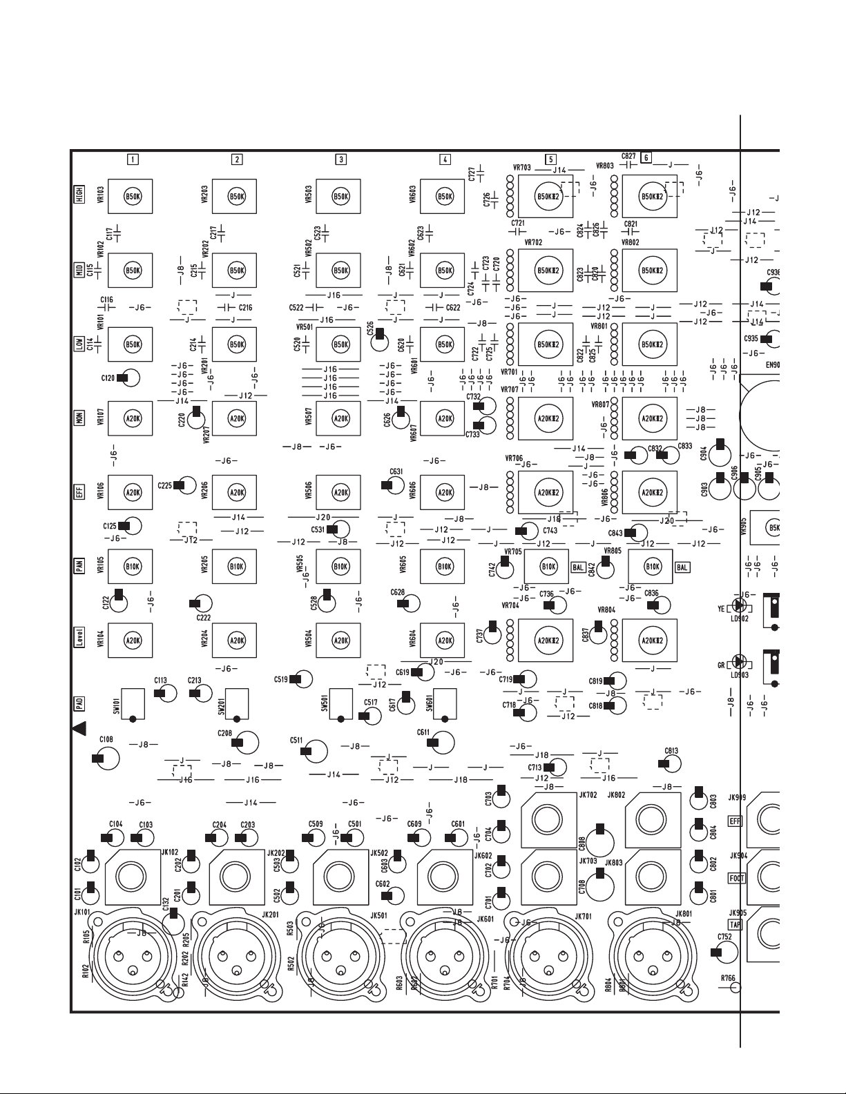
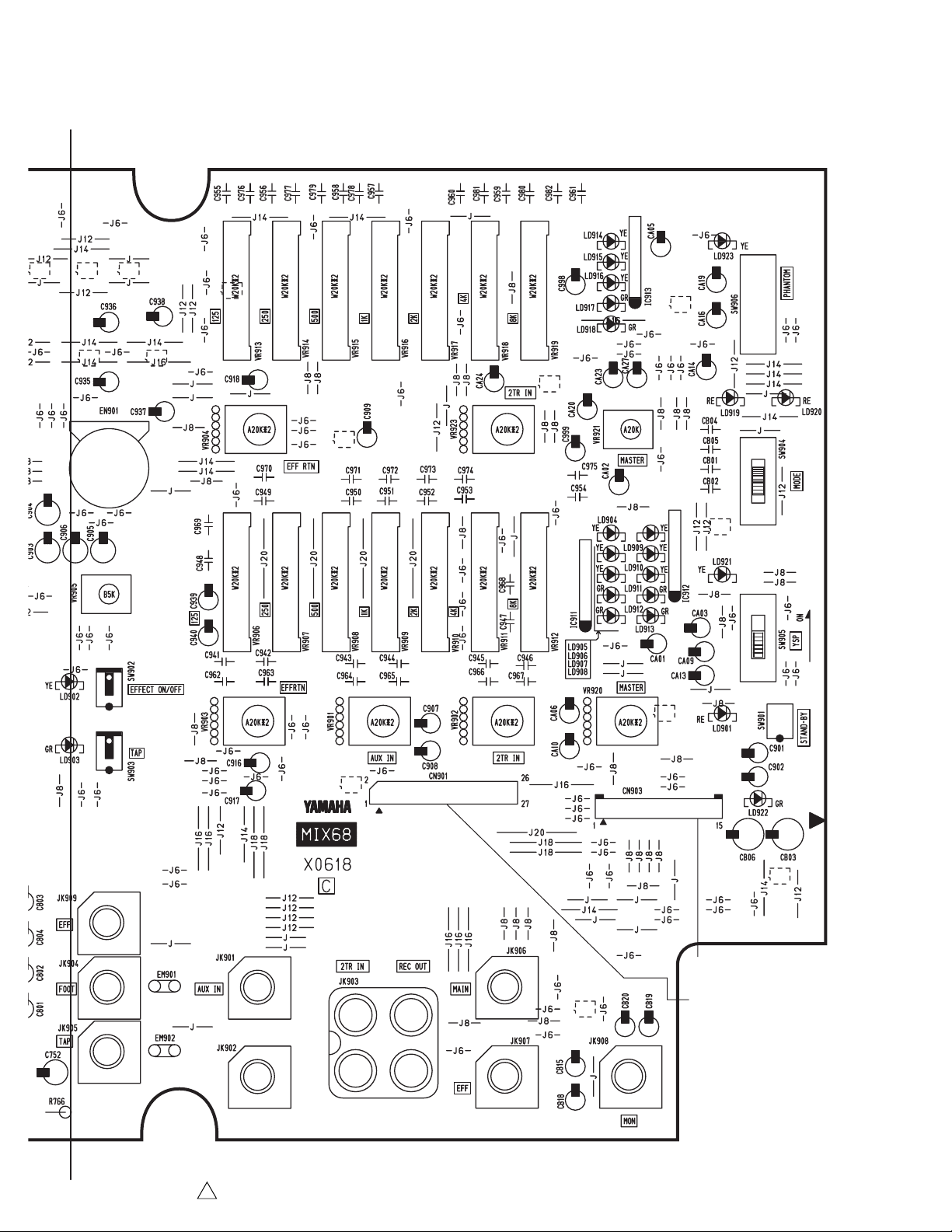
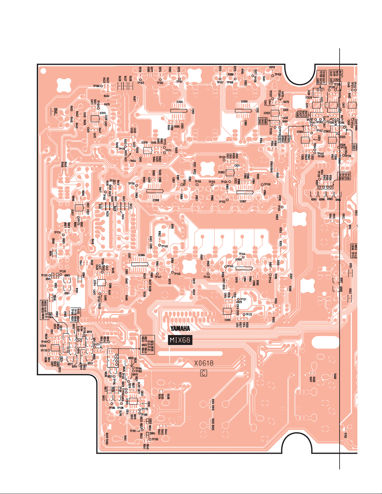
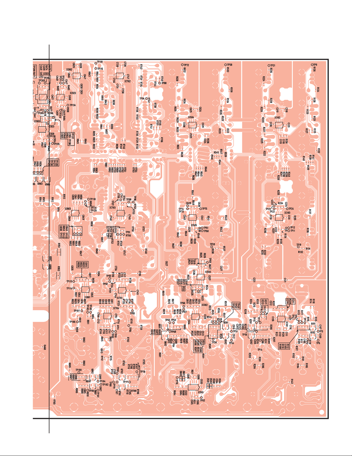
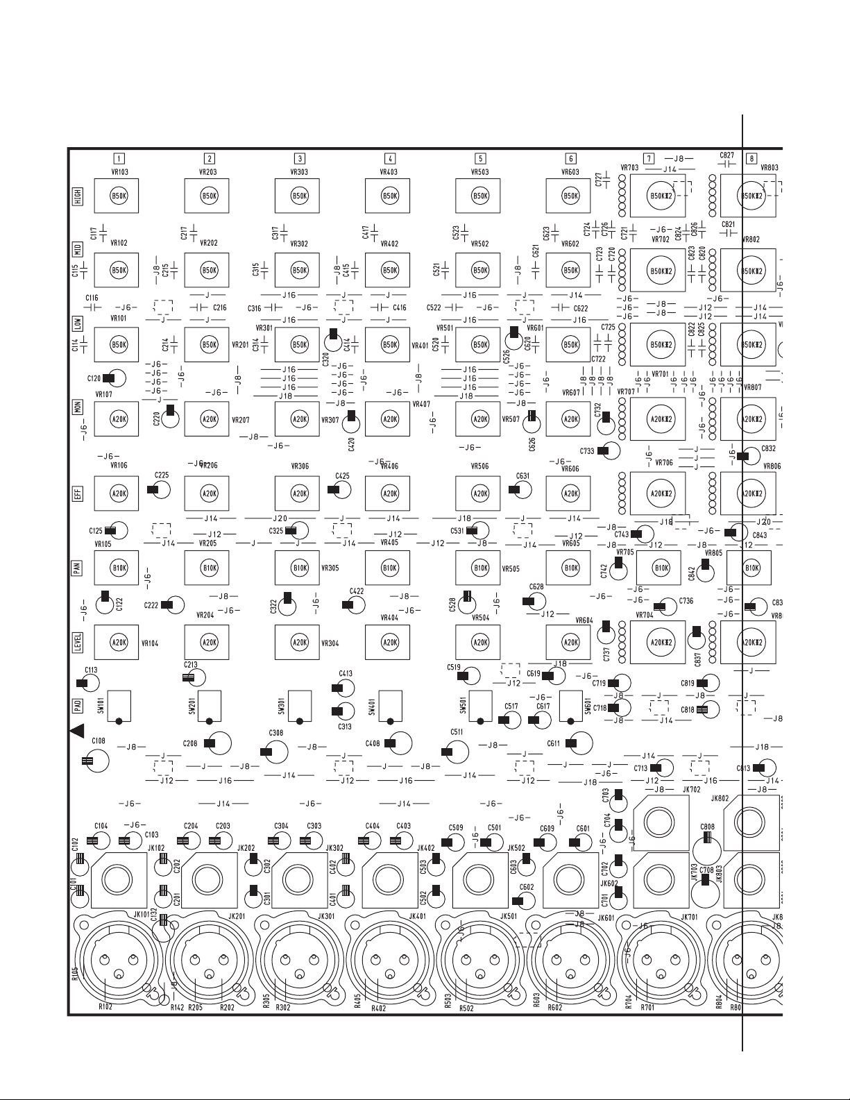
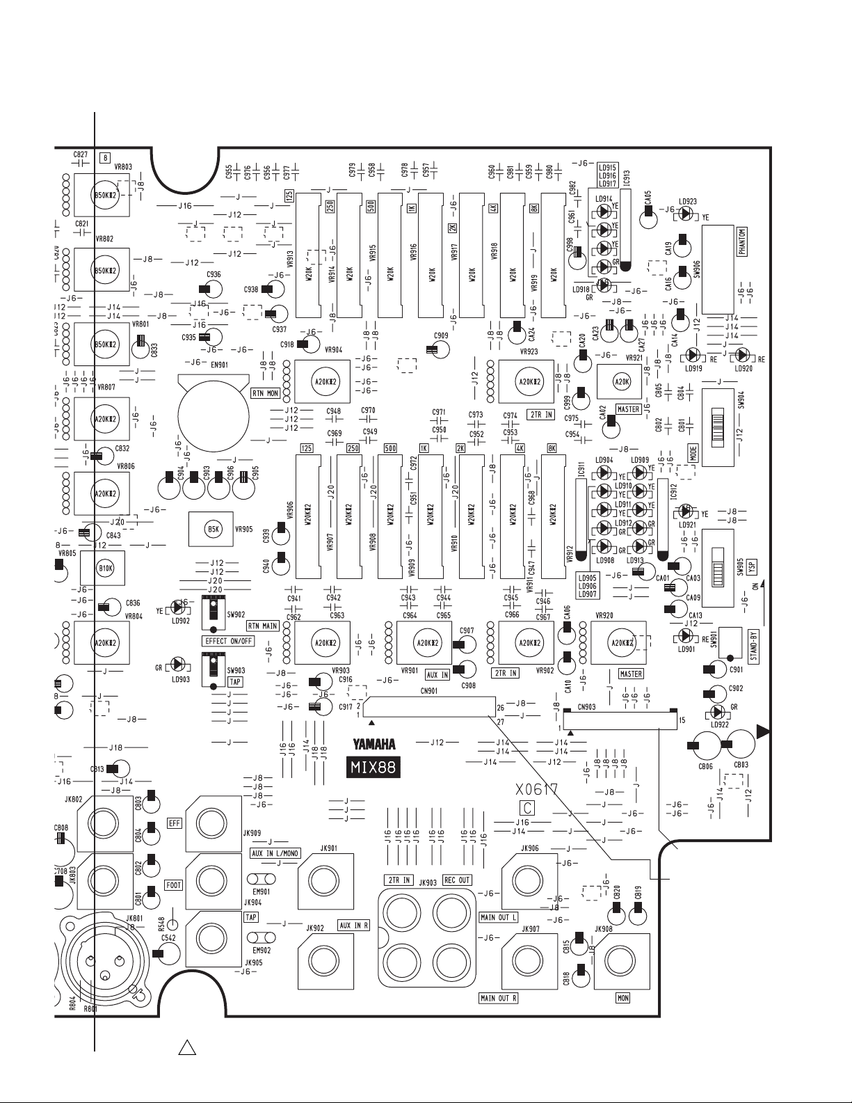
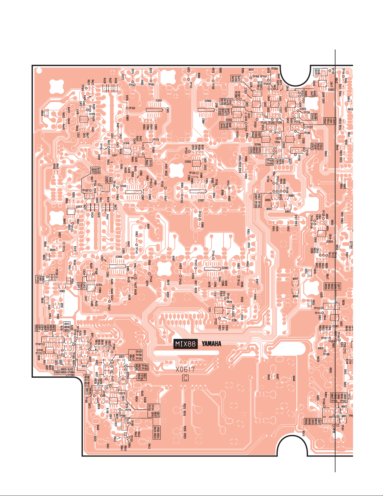
CIRCUIT BOARDS
CONTENTS
MIX68 CIRCUIT BOARD (COMPONENT SIDE) .................................................................................................24
MIX68 CIRCUIT BOARD (PATTERN SIDE) ........................................................................................................26
MIX88 CIRCUIT BOARD (COMPONENT SIDE) .................................................................................................28
MIX88 CIRCUIT BOARD (PATTERN SIDE) ........................................................................................................30
DSP CIRCUIT BOARD (COMPONENT SIDE) ....................................................................................................32
DSP CIRCUIT BOARD (PATTERN SIDE) ...........................................................................................................33
PWR 1/4 CIRCUIT BOARD (COMPONENT SIDE) .............................................................................................34
PWR 2/4 CIRCUIT BOARD (COMPONENT SIDE) .............................................................................................36
PWR 3/4 CIRCUIT BOARD (COMPONENT SIDE) .............................................................................................36
PWR 4/4 CIRCUIT BOARD (COMPONENT SIDE) .............................................................................................36
23
EMX68S / EMX88S
E
R
●
MIX68 Circuit Board
A
HIGH
MID
LOW
MONITOR
EFFECT
PAN
HIGH
MID
LOW
MONITOR
EFFECT
PAN
HIGH
MID
LOW
MONITOR
EFFECT
PAN
HIGH
MID
LOW
MONITOR
EFFECT
PAN
HIGH
MID
LOW
MONITOR
EFFECT
BAL/PAN
HIGH
MID
LOW
MONITOR
EFFECT
BAL/PAN
PROG
PARAMET
LEVEL
PAD
Hi-Z Hi-Z
LEVEL
PAD
LEVEL
PAD
Super Hi-Z Super Hi-Z
LEVEL
PAD
LEVEL
LINE L
LINE R
ON
LEVEL
TAP
LINE L
LINE R
24
Low-Z Low-Z Low-Z Low-Z MIC MIC
A'
EMX68S / EMX88S
A
R
PROGRAM
PARAMETER
ON
L
TAP
EFFECT RTN
EFFECT RTN
MONITOR
GRAPHIC
EQUALIZER
MAIN GRAPHIC
EQUALIZER
AUX IN
2TR IN
2TR IN
+6
+3
0
-5
-10
MASTER
MASTER
PHAMTOM
ON / OFF
POWER AMP
MODE
YAMAHA
SPEAKER
PROCESSING
STAND BY
A’
EFFECT OUT
EFFECT
ON/OFF
TAP
3NA-V826680 1
AUX IN L
AUX IN R
2TR IN L
2TR IN R
REC OUT L
REC OUT R
MAIN L
MAIN R
POWER
to PWR1/4-CN101
to DSP-CN101
MONITOR
Component side
25
EMX68S / EMX88S
●
MIX68 Circuit Board
A
26
A’
EMX68S / EMX88S
A
A'
Pattern side
27
EMX68S / EMX88S
P
D
N
●
MIX88 Circuit Board
A
HIGH
MID
LOW
MONITOR
EFFECT
PAN
HIGH
MID
LOW
MONITOR
EFFECT
PAN
HIGH
MID
LOW
MONITOR
EFFECT
PAN
HIGH
MID
LOW
MONITOR
EFFECT
PAN
HIGH
MID
MONITOR
EFFECT
PAN
LOW
HIGH
MID
LOW
MONITOR
EFFECT
PAN
HIGH
MID
LOW
MONITOR
EFFECT
BAL/PAN
HIGH
MI
LOW
MO
EFFECT
BAL/
LEVEL
PAD
Hi-Z Hi-Z
LEVEL
PAD
LEVEL
PAD
Hi-Z Hi-Z
LEVEL
PAD
LEVEL
PAD
Super Hi-Z Super Hi-Z
LEVEL
PAD
LEVEL
LINE L
LINE R
LEVEL
LINE L
LINE R
28
Low-Z Low-Z
Low-Z Low-Z
Low-Z Low-Z
MIC MIC
A'
A
HIGH
EMX68S / EMX88S
LOW
EFFECT
BAL/PAN
MID
MONITOR
ON
PROGRAM
PARAMETER
EFFECT RTN
MAIN GRAPHIC
EQUALIZER
MONITOR
GRAPHIC
EQUALIZER
2TR IN
+6
+3
0
-5
-10
PHAMTOM
ON / OFF
MASTER
POWER AMP
MODE
YAMAHA
SPEAKER
PROCESSING
LEVEL
LINE L
LINE R
MIC
TAP
EFFECT OUT
EFFECT
ON/OFF
TAP
EFFECT RTN
AUX IN L
AUX IN R
AUX IN
2TR IN L
2TR IN R
REC OUT L
REC OUT R
2TR IN
MAIN L
MAIN R
MASTER
MONITOR
STAND BY
POWER
to PWR1/4-CN101
to DSP-CN101
3NA-V826670 1
A’
Component side
29
EMX68S / EMX88S
●
MIX88 Circuit Board
A
30
A’
 Loading...