Yamaha EMX-5000 Service Manual
SERVICE MANUAL
本资料由OKXIA视听皮带资源库www.okxia.cn提供
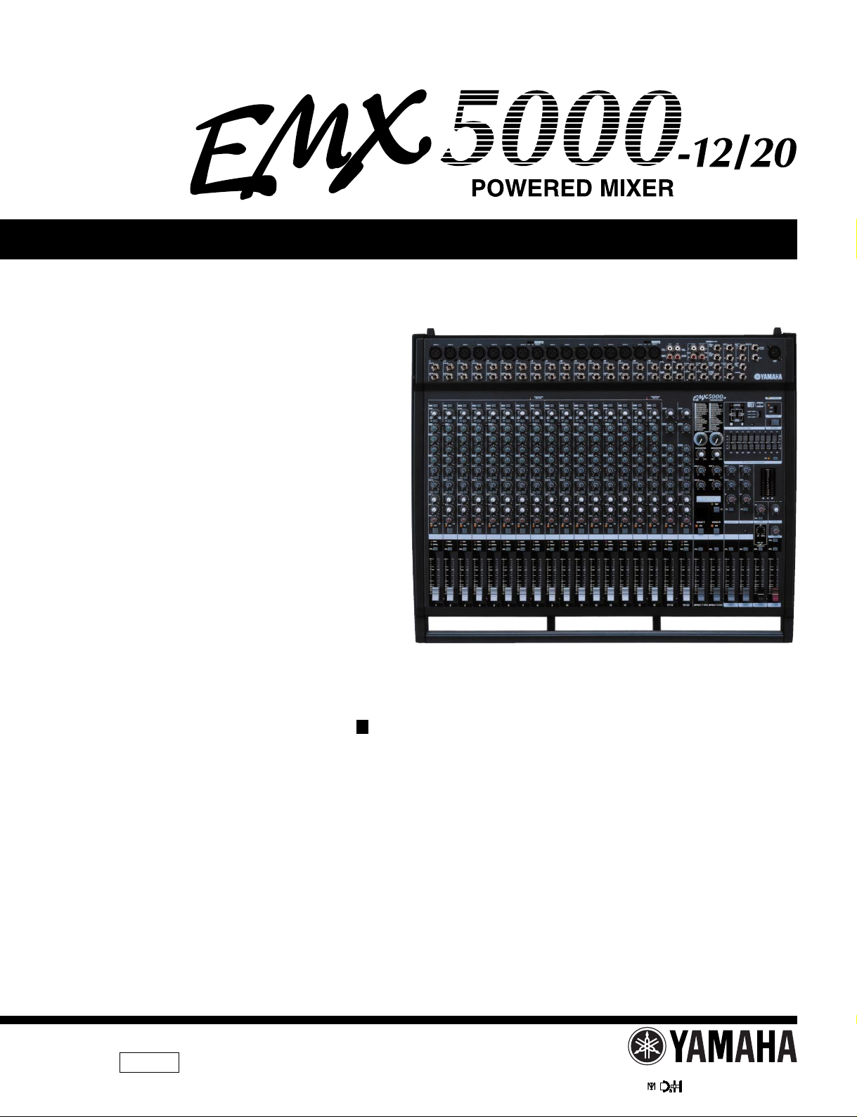
EMX5000-12/20
This document is printed on chlorine free (ECF) paper with soy ink.
011633
PA
EMX5000-20
CONTENTS
SPECIFICATIONS ................................................ 3/5
PANEL LAYOUT .................................... 7
CIRCUIT BOARD LAYOUT ............... 11
BLOCK & LEVEL DIAGRAM.......................................................
WIRING ................................................................... 14
DIMENSIONS .......................................................... 14
DISASSEMBLY PROCEDURE ............................ 15
LSI PIN DESCRIPTION .............................. 20
IC BLOCK DIAGRAM ................................. 23
CIRCUIT BOARDS ....................................... 24
INSPECTIONS ...................................................... 39/46
CIRCUIT DIAGRAMS ............................................. 54
PARTS LIST
HAMAMATSU, JAPAN
1.387K-9551 Printed in Japan 2002.3
12
1
EMX5000-12/20
IMPOR TANT NOTICE
This manual has been provided for the use of authorized Yamaha Retailers and their service personnel. It has been assumed
that basic service procedures inherent to the industry, and more specifically Yamaha Products, are already known and understood by the users, and have therefore not been restated.
WARNING : Failure to follow appropriate service and safety procedures when servicing this product may result in per-
IMPORTANT : This presentation or sale of this manual to any individual or firm does not constitute authorization certifi-
The data provided is belived to be accurate and applicable to the unit(s) indicated on the cover. The research engineering, and
service departments of Yamaha are continually striving to improve Yamaha products. Modifications are, therefore, inevitable
and changes in specification are subject to change without notice or obligation to retrofit. Should any discrepancy appear to
exist, please contact the distributor’s Service Division.
WARNING : Static discharges can destroy expensive components. Discharge any static electricity your body may have
IMPORTANT : Turn the unit OFF during disassembly and parts replacement. Recheck all work before you apply power
sonal injury, destruction of expensive components and failure of the product to perform as specified. For
these reasons, we advise all Yamaha product owners that all service required should be performed by an
authorized Yamaha Retailer or the appointed service representative.
cation, recognition of any applicable technical capabilities, or establish a principal-agent relationship of
any form.
accumulated by grounding yourself to the ground bus in the unit (heavy gauge black wires connect to
this bus.)
to the unit.
WARNING: CHEMICAL CONTENT NOTICE!
The solder used in the production of this product contains LEAD. In addition, other electrical/electronic and/or plastic (Where
applicable) components may also contain traces of chemicals found by the California Health and Welfare Agency (and possibly
other entities) to cause cancer and/or birth defects or other reproductive harm.
DO NOT PLACE SOLDER, ELECTRICAL/ELECTRONIC OR PLASTIC COMPONENTS IN YOUR MOUTH FOR ANY REASON WHAT
SO EVER!
Avoid prolonged, unprotected contact between solder and your skin! When soldering, do not inhale solder fumes or expose
eyes to solder/flux vapor!
If you come in contact with solder or components located inside the enclosure of this product, wash your hands before handling
food.
WARNING: THIS APPARATUS MUST BE EARTHED
IMPORTANT
THE WIRES IN THIS MAINS LEAD ARE COLOURED IN
ACCORDANCE WITH THE FOLLOWING CODE:
GREEN-AND-YELLOW : EARTH
BLUE : NEUTRAL
BROWN : LIVE
As the colours of the wires in the mains lead of this apparatus may
not correspond with the coloured markings identifying the terminals in
your plug, proceed as follows:
The wire which is coloured GREEN and YELLOW must be
connected to the terminal in the plug which is marked by the letter E
or by the safety earth symbol or coloured GREEN and YELLOW.
The wire which is coloured BLUE must be connected to the terminal
which is marked with the letter N or coloured BLACK.
The wire which is coloured BROWN must be connected to the
terminal which is marked with the letter L or coloured RED.
* This applies only to products distributed by YAMAHA KEMBLE
MUSIC (U.K.) LTD.
WARNING
Components having special characteristics are marked and must be
replaced with parts having specification equal to those originally installed.
This mark urges servicemen to pay attention.
2
SPECIFICATIONS
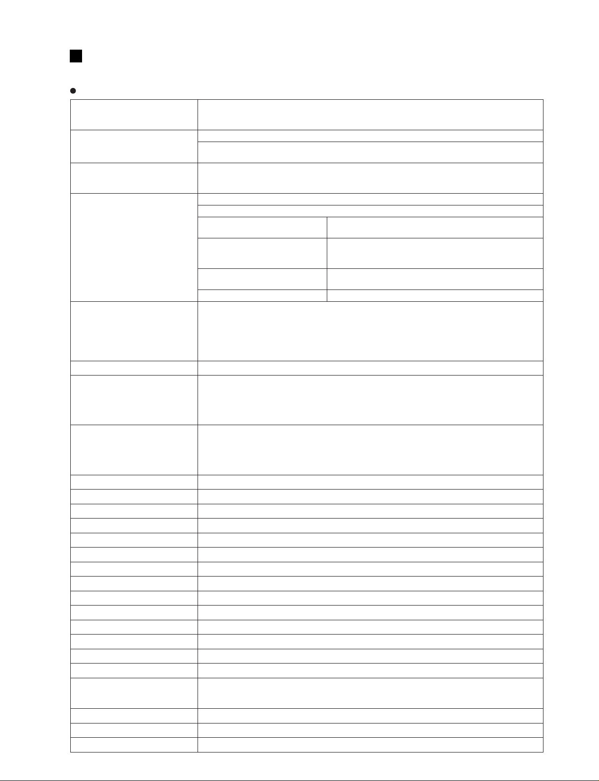
General specifications
Maximum output power
Frequency response
Total harmonic distortion
Hum & noise
(Average, Rs=150Ω)
(with 20 Hz–20 kHz BPF)
Maximum voltage gain
Crosstalk at 1 kHz
Input channel equalization
ST Input channel equalization
CH peak indicators
CH signal indicators
Meters
Power amp select switch
Limiter
LIMIT indicators
Graphic equalizer
Internal digital effect 1
Internal digital effect 2
Foot switch (FC5)
Protection circuit (Power amp)
Fan circuit
Phantom power
Option
Power requirement/
Power consumption
Dimensions (WxHxD)
Weight
Accessories
EMX5000-12/20
SPEAKERS: 500 W+500 W/4Ω @0.5% THD at 1 kHz
BRIDGE: 1000 W/8Ω @0.5% THD at 1 kHz
20 Hz–20 kHz +1 dB, –3 dB @1 W output into 8Ω (SPEAKERS OUT)
20 Hz–20 kHz +1 dB, –3 dB @+4 dB output into 600Ω
(ST OUT, ST SUB OUT, MONO OUT, AUX SEND, EFFECT SEND)
Less than 0.5% @20 Hz–20 kHz, 250 W output into 4Ω (SPEAKERS OUT)
Less than 0.3% @20 Hz–20 kHz, +14 dB output into 600Ω
(ST OUT, ST SUB OUT, MONO OUT, AUX SEND, EFFECT SEND)
–128 dB equivalent input noise, –65 dB residual output noise (SPEAKERS OUT)
–95 dB residual output noise (ST OUT, ST SUB OUT, AUX SEND)
–84 dB (ST OUT, MONO OUT)
–64 dB (68 dB S/N)
(ST OUT, MONO OUT)
–81 dB (AUX SEND)
–80 dB (EFFECT SEND) All channel level control at minimum.
108 dB INPUT A/B to SPEAKERS OUT
84 dB INPUT A/B to ST OUT, MONO OUT
80 dB INPUT A/B to AUX SEND (PRE)
90 dB INPUT A/B to AUX SEND (POST)
78 dB INPUT A/B to EFFECT SEND
58 dB ST CH IN to ST OUT
68 dB adjacent input, 68 dB input to output
±15 dB Maximum
HIGH 10 kHz shelving*
MID 250 Hz–5 kHz peaking
LOW 100 Hz shelving*
* Turn over/roll off frequency of shelving: 3 dB below maximum variable level.
±15 dB Maximum
HIGH 10 kHz shelving*
MID 2.5 kHz peaking
LOW 100 Hz shelving*
* Turn over/roll off frequency of shelving: 3 dB below maximum variable level.
Red LED on each channel lits when POST EQ signal reaches the level –3 dB below clipping.
Green LED on each channel lits when POST EQ signal reaches the level –10 dB.
13 points LED meter
500W + 500W, 300W + 300W, 100W + 100W
Comp. : THD≥0.5% (SPEAKERS OUT)
Turn on : THD≥0.5% (SPEAKERS OUT)
9 bands (63, 125, 250, 500, 1k, 2k, 4k, 8k, 16k Hz), ±12 dB Maximum
16 programs, parameter control
16 programs, parameter control, tap delay control, foot switch (DIGITAL EFFECT ON/OFF, TAP)
Digital effect 2 mute: on/off, Tap delay
POWER switch on/off mute, DC detection, TEMP (heatsink temp. ≥90°C)
stop — low speed (50°C) — variable — high speed (70°C)
+48 V (balanced input)
FC5 (Foot switch), RK-124 (EMX5000-12)
USA and Canada:120 V AC 60 Hz, 400 W
Europe: 230 V AC 50 Hz, 550 W
Other: 240 V AC 50 Hz, 550 W
682 × 158 × 538 mm (EMX5000-20) / 478 × 158 × 538 mm (EMX5000-12)
19 kg (EMX5000-20) / 15 kg (EMX5000-12)
Power cord, Owner’s Manual
325 W+325 W/8Ω @0.5% THD at 1 kHz
ST master/MONO master fader at nominal level and all channel On switches off and all channel fader at minimum.
ST master fader at nominal level and one channel On switch
on and one channel fader at nominal level and one channel
Gain control at nominal level.
Master fader at nominal lev el and all channel On s witches off
and all channel level control at minimum.
3
EMX5000-12/20
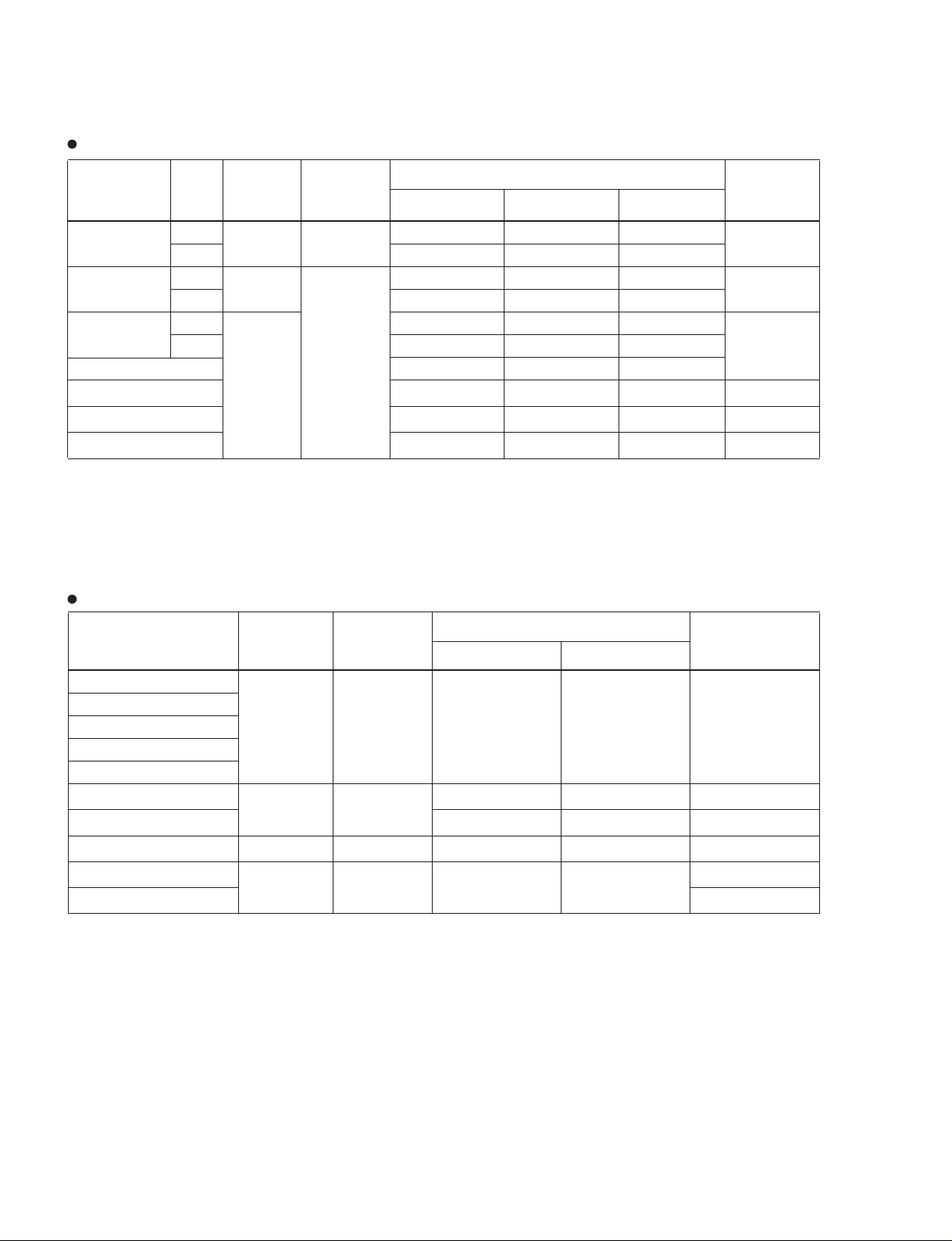
Input specifications
Gain
Input terminals
CH INPUT A
(CH1–8/1–16)
CH INPUT B
(CH1–8/1–16)
ST INPUT
(CH9–12/17–20)
ST SUB IN (1, 2) –12 dB (195 mV) +4 dB (1.23 V) +20 dB (7.75 V)
2TR IN (L, R) –26 dBV (50.1 mV) –10 dBV (316 mV) +10 dBV (3.16 V)
INSERT IN (CH1–8/1–16) –20 dB (77.5 mV) 0 dB (0.775 V) +20 dB (7.75 V)
POWER AMP IN (A, B) –12 dB (195 mV) +4 dBV (1.23 V) +18 dB (6.16 V)
1. Sensitivity is the lowest level that can produce an output of +4 dB (1.23 V) or the nominal output le v el when the unit is set at maximum gain.
(All fader and level controls are at maximum position.)
2. Balanced. (T=HOT, R=COLD, S=GND)
3. Unbalanced.
In these specifications when dB represents a specific voltage, 0 dB is referenced to 0.775 Vrms, 0 dBV is referenced to 1 Vrms.
control
Actual load
impedance
–60
–16 –36 dB (12.3 mV) –16 dB (123 mV) +4 dB (1.23 V)
–60
–16 –36 dB (12.3 mV) –16 dB (123 mV) +4 dB (1.23 V)
–34
+10 –10 dB (245 mV) +10 dB (2.45 V) +30 dB (24.5 V)
5 kΩ 50–600Ω Mics
50 kΩ
10 kΩ
For use with
nominal
600Ω Lines
Sensitivity
–80 dB (0.078 mV) –60 dB (0.775 mV) –40 dB (7.75 mV)
–80 dB (0.078 mV) –60 dB (0.775 mV) –40 dB (7.75 mV)
–54 dB (1.55 mV) –34 dB (15.5 mV) –14 dB (155 mV)
1
Input level
Nominal Max. before clip
Connectors on
XLR-3-31 type
PHONE JACK
(TRS)
PHONE JACK
PHONO JACK
PHONE JACK
PHONE JACK
Output specifications
Output terminals
ST OUT (L/R)
ST SUB OUT (L/R)
MONO OUT
AUX SEND 1, 2
EFFECT SEND 1, 2
REC OUT (L/R)
INSERT OUT (CH1–8/1–16) 0 dB (775 mV) +20 dB (7.75 V)
PHONES (L/R) 100Ω 40Ω Lines 3 mW 75 mW
SPEAKERS 1 (A, B)
SPEAKERS 2 (A, B)
1. Unbalanced.
2. Impedance balaned. (T=HOT, R=COLD, S=GND)
• In these specifications when dB represents a specific voltage, 0 dB is referenced to 0.775 Vrms, 0 dBV is referenced 1 Vrms.
Actual source
impedance
150Ω 600Ω Lines +4 dB (1.23 V) +20 dB (7.75 V)
600Ω 10 kΩ Lines
0.1Ω 4/8Ω Speakers 100 W/4Ω 500 W/4Ω
For use with
nominal
Nominal Max. before cliping
–10 dBV (316 mV) +10 dBV (3.16 V)
Output level
Connectors on mixer
PHONE JACK
PHONO JACK
PHONE JACK
PHONE JACK (TRS)
SPEAKON
PHONE JACK
mixer
2
2
3
3
3
3
1
1
1
2
1
For European Model
Purchaser/User Information specified in EN55103-1 and EN55103-2.
Inrush Current: 70A
Conformed Environment: E1, E2, E3 and E4
4

EMX5000-12/20
5

EMX5000-12/20
6
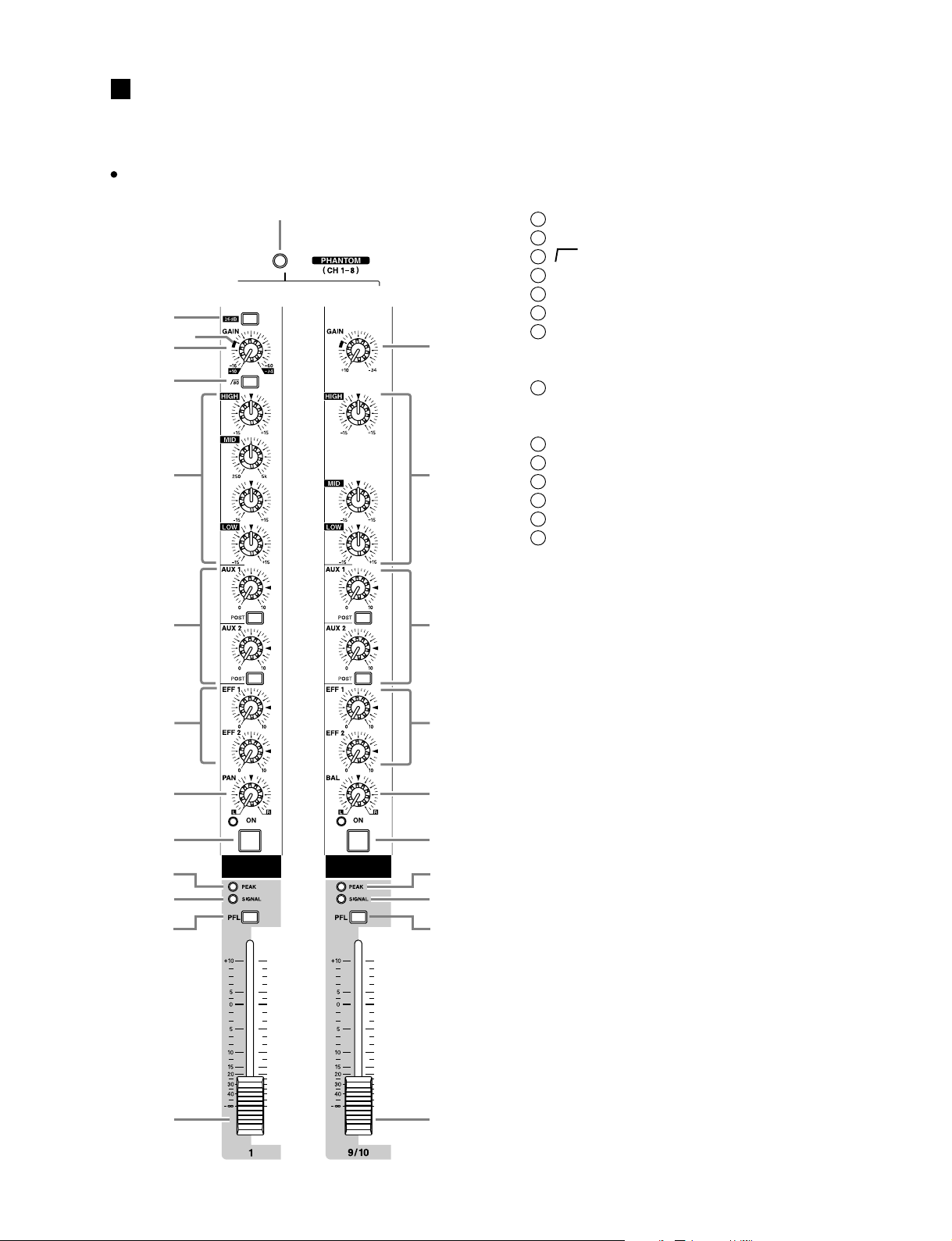
PANEL LAYOUT
Control Panel
Channel Control Section
EMX5000-12/20
q
w
e
r
t
!4
*
w
r
1
26 dB pad switch
2
GAIN control
3
80 (High pass filter) switch
4
Equalizer controls (HIGH, MID, LOW)
5
AUX1, AUX2 controls / POST switches
6
EFF 1, 2 controls (EFFECT)
7
PAN (panpot) control
(EMX5000-20: Cannels 1-16,
EMX5000-12: Cannels 1-8)
8
BAL (balance) control
(EMX5000-20: Cannels 17/18-19/20,
EMX5000-12: Cannels 9/10-11/12)
9
ON switch, indicator
10
PEAK indicator
11
SIGNAL indicator
12
PFL (pre-fader listen) switch
13
Channel fader
14
PHANTOM indicator
t
yy
u
o
!0
!1
!2
!3
i
o
!0
!1
!2
!3
7
EMX5000-12/20
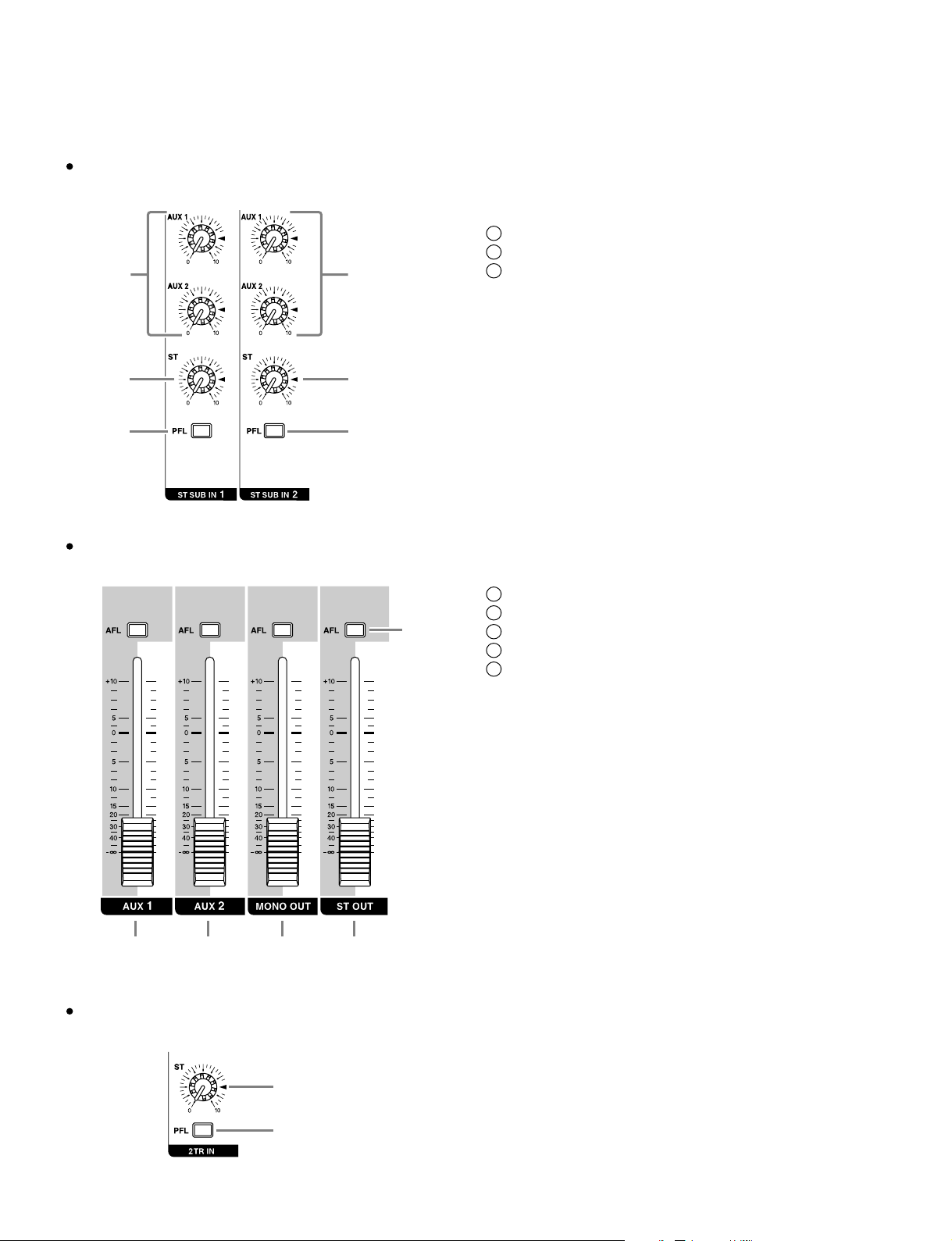
Stereo Sub Input Section
!5
!5
AUX 1, 2 controls
15
ST (stereo) control
16
PFL (pre-fader listen) switch
17
!6
!7
Master Control Section
!6
!7
@2
AUX 1 fader
18
AUX 2 fader
19
MONO OUT fader
20
ST OUT fader
21
AFL (after fader listen) switch
22
2TR IN Section
8
!8 !9 @0 @1
@3
@4
ST (stereo) control
PFL (pre-fader listen) switch
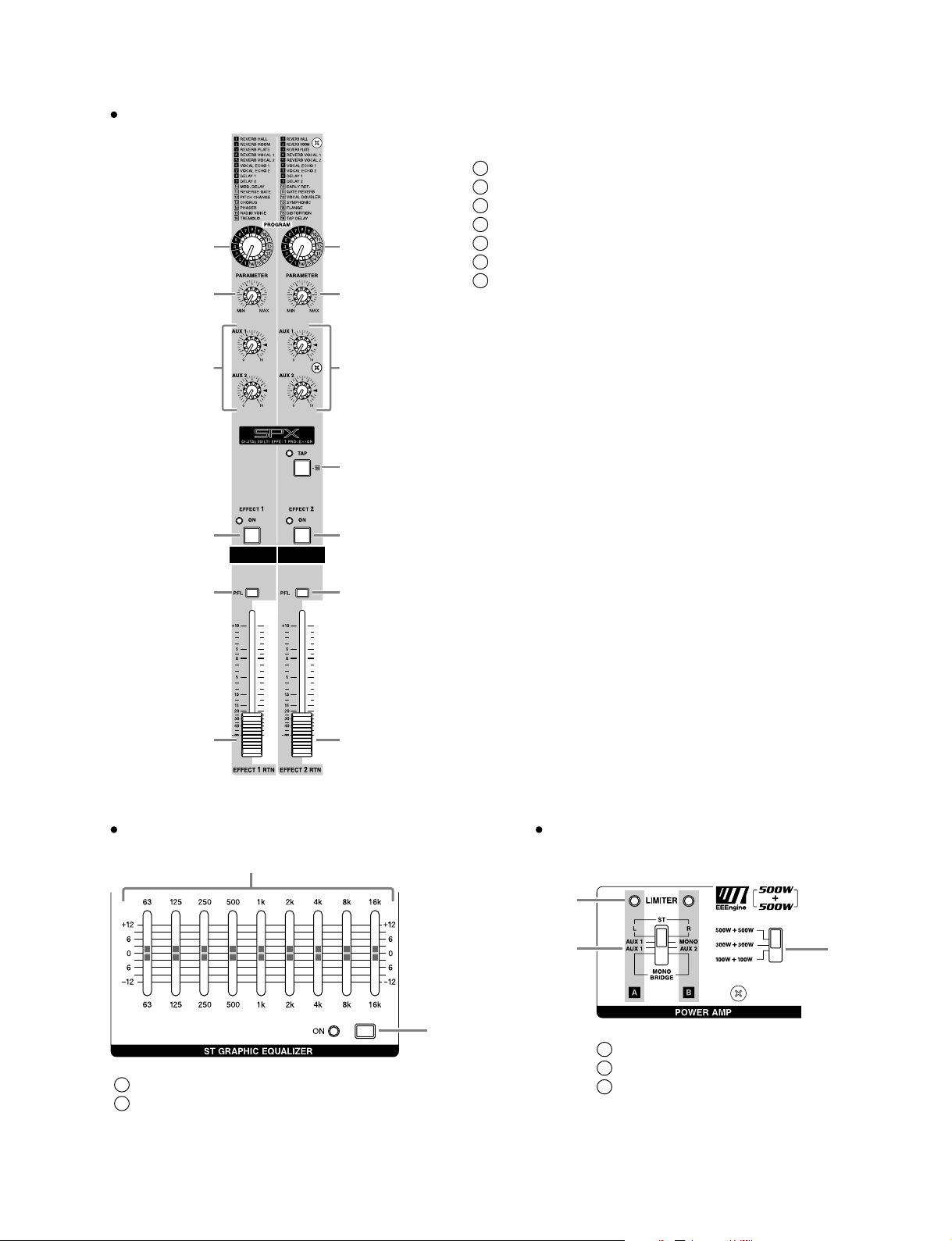
Digital effect Section
@5@5
@6@6
@7@7
@8
PROGRAM selector
25
PARAMETER control
26
AUX 1/2 control
27
TAP switch, indicator
28
EFFECT 1/2 ON switch
29
PFL (Pre-fader listen) switch
30
EFFECT 1/2 RTN fader
31
EMX5000-12/20
Graphic equalizer Section
#2
@9@9
#0#0
#1#1
Power amp Section
#4
#5
#6
Graphic equalizer
32
ON switch
33
#3
LIMITER indicator
34
Power amp select switch
35
Maximum output select switch
36
9
EMX5000-12/20
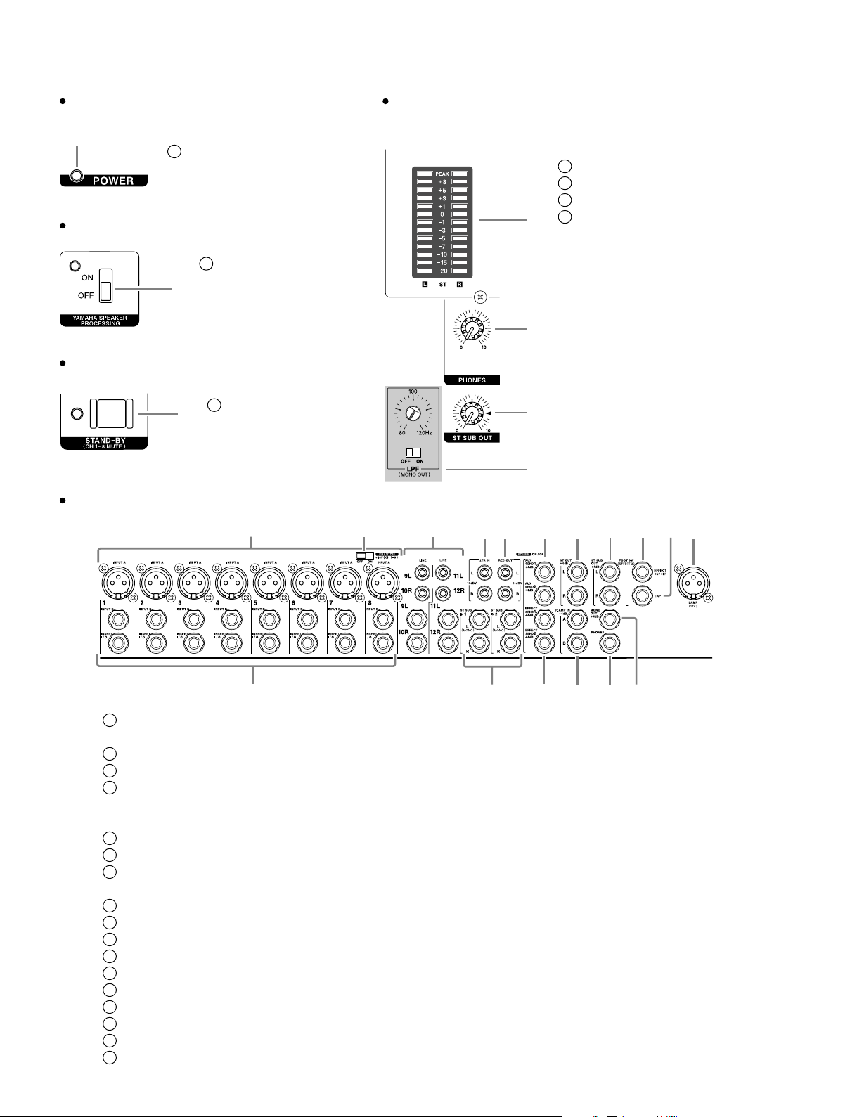
POWER indicator
#7
POWER indicator
37
YAMAHA SPEAKER PROCESSING
38
ON/OFF switch
#8
STAND-BY
ON/OFF switch
39
#9
Input/Output pabel
Other indicators and controls
40
41
42
43
$0
$1
$2
$3
Peak level indicator
PHONES control
ST SUB OUT control
LPF control, ON/OFF switch
10
q
w
1
Channel input jacks (INPUT A, INPUT B)
EMX5000-20: 1–16, EMX5000-12: 1–8
2
INSERT I/O (insert) jacks
3
PHANTOM switch
4
LINE (stereo) input jacks
EMX5000-20: 17/18–19/20,
EMX5000-12: 9/10–11/12
5
2TR IN jacks
6
REC OUT jacks
7
ST SUB IN 1 (stereo sub 1) jacks
ST SUB IN 2 (stereo sub 2) jacks
8
AUX SEND 1 jack, AUX SEND 2 jack
9
EFFECT SEND 1 jack, EFFECT SEND 2 jack
10
ST OUT jacks
11
ST SUB OUT jacks
12
P.AMP IN A, B (power amp input) jacks
13
MONO OUT jack
14
PHONES jack
15
FOOT SW EFFECT 2 ON/OFF jack
16
FOOT SW (EFFECT 2) TAP jack
17
LAMP jack
re
u
!0
o!2
!1ty i
!4
!5 !6
!3
!7
EMX5000-12/20
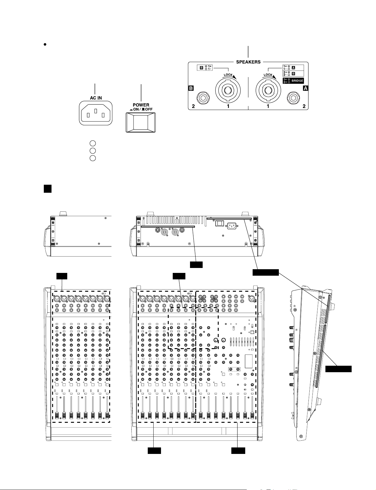
Rear panel
wq
1
AC inlet
2
POWER switch
3
SPEAKERS (speaker output) jacks
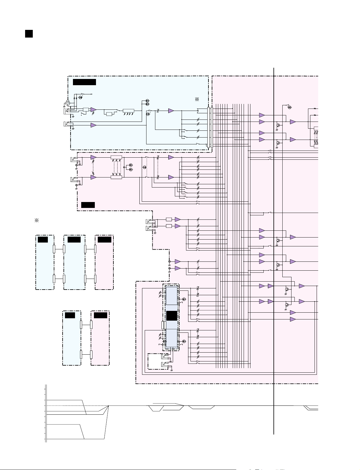
CIRCUIT BOARD LAYOUT
e
IN8 DSP
PWR
SMPS 1/2
SMPS 2/2
EMX5000-20 only
IN16 MAS
11
EMX5000-12/20
9
9
250Hz
T
M
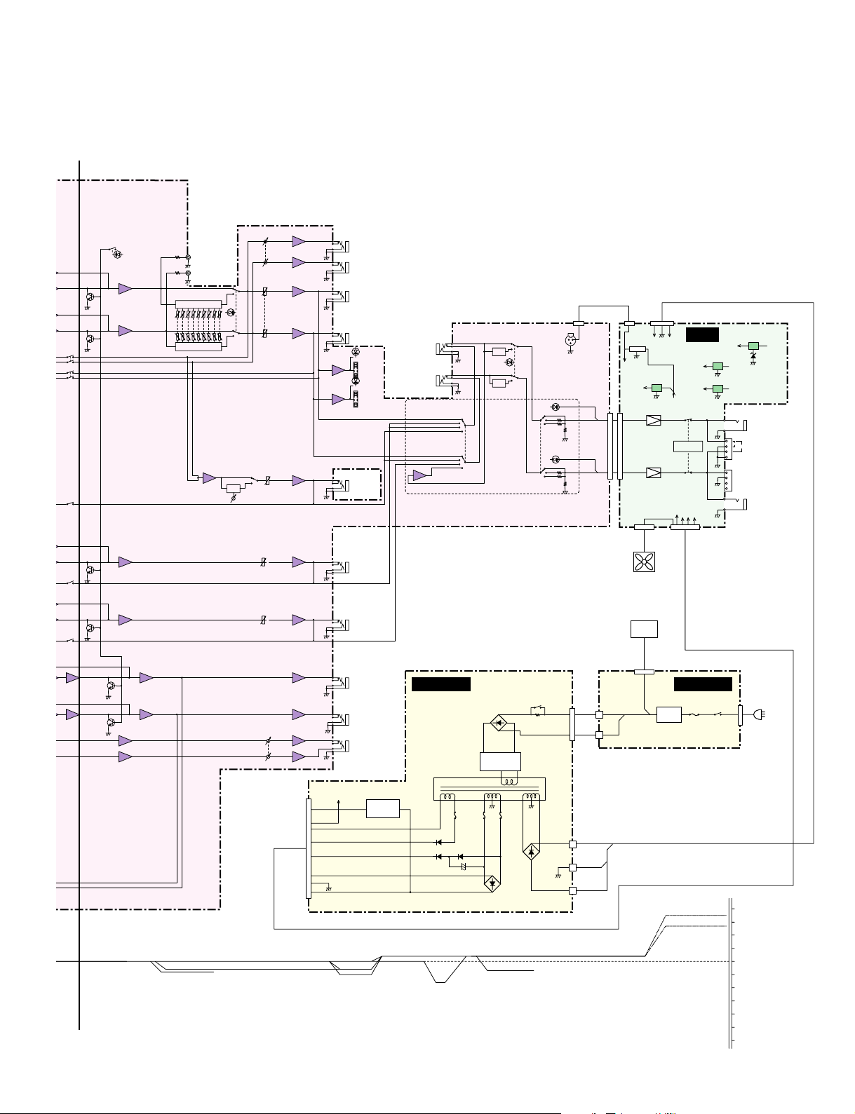
BLOCK & LEVEL DIAGRAM
CH INPUT
[–60~–16dB]
[–34~+10dB]
EMX5000-12:CH1-8
EMX5000-20:CH1-16
CH INSERT I/O
[0dB]
EMX5000-12:CH1-8
EMX5000-20:CH1-16
ST CH INPUT
[–34~+10dB]
EMX5000-12:CH9(L)/10(R),CH11(L)/12(R)
EMX5000-20:CH17(L)/18(R),CH19(L)/20(R)
A
B
IN8/IN16
L
R
+48V
PHANTOM
8CH/SW
EMX5000-12:[CH1-8]
EMX5000-20:[CH1-8] [CH9-16]
IC101,201,301,401,501,601,701,801
[0dB]
PAD
HA
GAIN
[–60~–16dB]
[–34~+10dB]
BA
HA
GAIN
[–34~+10dB]
HA
HPF
[0dB]
[0dB]
26dB
IC101,
102,
201,
202
IC505,705
IC105,305
IC101,102,
201,202
HPF
3-Stage EQ
Lo
Mid
3-Stage EQ
Hi
3-Stage EQ
Mid f
Lo Gain
[0dB]
Mid Gain
[0dB]
Hi Gain
PEAK
SIGNAL
DN
PEAK
SIGNAL
CH Fader
ON
IC107,307,
507,707
[–10dB]
[–10dB]
IC104,204
ST CH Fader
IC104,204
A
STEREO L (NON-MUTE)
STEREO R (NON-MUTE)
EFFECT1 (NON-MUTE)
EFFECT2 (NON-MUTE)
AUX1 (NON-MUTE)
AUX2 (NON-MUTE)
STEREO L (MUTE)
STEREO R (MUTE)
EFFECT1 (MUTE)
EFFECT2 (MUTE)
AUX1 (MUTE)
AUX2 (MUTE)
PFL L / AFL L
[0dB]
CN903, 904
BA
EFFECT1
EFFECT2
AUX1
POST
AUX2
POST
PFL
[0dB]
BA
BA
EFFECT1
EFFECT2
POST
POST
BAL
AUX1
AUX2
PAN
[0dB]
[–6dB]
[–6dB]
[–6dB]
[–6dB]
[–6dB]
CN603, 604
[0dB]
[–6dB]
[–6dB]
[–6dB]
PFL R / AFL R
IC302
[0dB]
67
SUM
[0dB]
67
SUM
IC301
IC302
[0dB]
21
SUM
[0dB]
21
SUM
IC301
PFL
AFL
STAND-BY
Q303
Q304
67
21
EMX5000-12:CH1-8
EMX5000-20:CH1-16
IC303
[0dB]
SUM
IC303
[0dB]
SUM
63Hz
125Hz
EMX5000-20
IN8
CN904
CN903
EMX5000-12
CN902
CN901
IN8
CN904
CN903
CN904
CN903
MAS
CN604
CN603
MAS
CN604
CN603
PFL
IC501
IC502
[+4dB] [–6dB]
R
ST SUB IN 1,2
[+4dB]
L (MONO)
MASIN16
2TR IN
[–10dBV]
PROGRAM
PARAMETER
CN501
35P
PROGRAM
PARAMETER
TAP
ON/OFF
FOOT SWITCH
TAP
PAD
PAD
L
R
IN
L OUT
R OUT
DIGITAL
EFFECT1
DSP
-SPX
CN101
35P
IN
L OUT
R OUT
DIGITAL
EFFECT2
[0dB]
BA
BA
IC501
IC502
IC503
[0dB]
57
BA
31
BA
IC503
[–6dB]
[–6dB]
ST
[–6dB]
AUX1
[–6dB]
AUX2
PFL
[–6dB]
ST
PFL
[–16dB]
EFFECT1 RTN
[–12dB]
ON
AUX1
[–12dB]
AUX2
PFL
[–16dB]
EFFECT2 RTN
[–12dB]
ON
AUX1
[–12dB]
AUX2
PFL
AFL
IC306
[0dB]
21
SUM
[0dB]
67
SUM
IC305
AFL
IC306
[0dB]
67
SUM
[0dB]
2
1
SUM
IC305
AFL
672
IC307
67
2
SUM
IC308
IC309
[0dB]
21
SUM
IC309
[0dB]
67
SUM
IC504
67
SUM
IC504
21
SUM
IC310
21
SUMSUM
IC310
[–6dB]
67
SUM
[0dB]
[0dB]
[–6dB]
1
[0dB]
INV
Q307
1
[0dB]
INV
Q308
12
0dB=0.775V
0dBV=1V
+30dB
+20dB
ST CH INPUT
GAIN Min. [+10dB]
+10dB
0dB
–10dB
CH INPUT A, B GAIN Min. [–16dB]
–20dB
ST CH INPUT
–30dB
GAIN Max. [–34dB]
–40dB
–50dB
CH INPUT A, B
GAIN Max. [–60dB]
–60dB
fader [–10dB]
ST SUB IN [+4dB]
2TR IN [–10dBV]
CH & ST CH to ST [0dB] (PAN, BAL turned hard left/right)
CH & ST CH to AUX/EFFECT [–6dB]
ST SUB IN to ST/AUX [–6dB]
2TR IN to ST [–6dB]
REC OU
A
2
1
2
1
6
5
6
5
72
7
EMX5000-12/20
A
IC316
IC316
JK301
L
ST SUB OUT
[+4dB]
JK302
R
JK303
L
ST OUT
1
8
8
IC601
DR
IC602
DR
JK305
R
PEAK
PEAK
MONO OUT
[+4dB]
JK602
A
POWER AMP IN
[+4dB]
JK601
MONO BRIDGE
MONO BRIDGE
31
INV
IC604
B
MAIN L
AUX1
AUX1
Signal Select
MAIN R
MONO
AUX2
[+4dB]
JK304
YAMAHA
SPEAKER
PROCESSING
YSP
YSP
POWER AMP Controls
CN602
LAMP
LIMITTER
500W
300W
100W
Power Select
LIMITTER
500W
300W
100W
2P
CN105
CN601
15P 15P
IC105
CN101
CN104
2P
CN102 VH3P
+12V
+5V
+B -B
IC104
PA
A
PA
B
PWR
+15V +21V
-15V -21V
LAMP
PROTECTOR
LAMP
+63V
-21V
IC101
IC102
+12V
IC103, Q136
+48V +63V
JK101
2
1
A
+1
A
–1
BRIDGE
+2
–2
SPEAKERS
1
[500Wmax@4ohms]
+1
–1
+2
–2
B
2
JK102
CN103-10P
JK306
JK307
JK308
JK309
JK508
AUX SEND1
[+4dB]
AUX SEND2
[+4dB]
EFFECT SEND1
[+4dB]
EFFECT SEND2
[+4dB]
PHONES
[3mW@40ohms]
D102
SWITCHING
REGULATOR
RY101
VH3P
CN103
W101
W101
FAN
COIL
VH2P
CN102
SMPS 1/2SMPS 2/2
AC
YE
LINE
FILTER
F101 POWER
BR
INLET
SW101
[–6dB]
57
MONO OUT
LPF
AUX1
AUX2
VR515
ST SUB OUT
[–10dB]
ST OUT
[–10dB]
[–10dB]
[–10dB]
[–16dB]
BA
31
BA
IC317
57
BA
IC317
3
BA
IC319
INV
21
IC320
57
BA
IC320
31
BA
IC321
21
INV
IC321
67
INV
IC505
INV
21
INV
67
IC505
STAND-BY
EMX5000-12:CH1-8
[0dB]
7
[0dB]
7
[0dB]
1
[0dB]
1
PFL
AFL
AFL
[0dB]
1
[0dB]
7
AFL
[0dB]
7
[0dB]
1
AFL
INV
307
2
INV
308
EMX5000-20:CH1-16
IC303
[0dB]
67
SUM
Q303
IC303
[0dB]
21
SUM
Q304
IC309
[0dB]
21
SUM
IC309
[0dB]
67
SUM
IC504
67
SUM
IC504
21
SUM
IC310
21
SUM
IC310
67
SUM
[0dB]
[0dB]
1
[0dB]
Q307
1
[0dB]
Q308
[–6dB]
[–6dB]
MAIN GEQ
9-Stage GEQ
63Hz
125Hz
250Hz
9-Stage GEQ
JK505
L
REC OUT
[–10dBV]
R
1kHz
2kHz
500Hz
IC318
67
SUM
GEQ
4kHz
8kHz
16kHz
LPF
80–120Hz
FREQ
(12dB/oct)
PHONES
D106,
D107
T104
W102
W102
W102
BE
BL
BE
MAXIMUM OUTPUT POWER 500W/4
SPEAKERS OUT
100W/4
+40dB
+30dB
+20dB
+10dB
0dB
–10dB
–20dB
REC OUT [–10dBV]
EFFECT [–6dB]
CN104
(LAMP) +17V
10P
+63V
-21V
+12V
ST SUB level control [–6dB]
OFF DETECT
Q111~115
CONTROL
OV
ST•MONO•AUX fader [–10dB]
FAN
F104
D114
D113
ST OUT•ST SUB OUT•MONO OUT [+4dB]
AUX SEND, EFFECT SEND [+4dB]
PHONES [–16dB]
F103 F102
D112
D108-D111
[PHONES 3mW@40ohms]
–30dB
–40dB
–50dB
A
–60dB
13
EMX5000-12/20
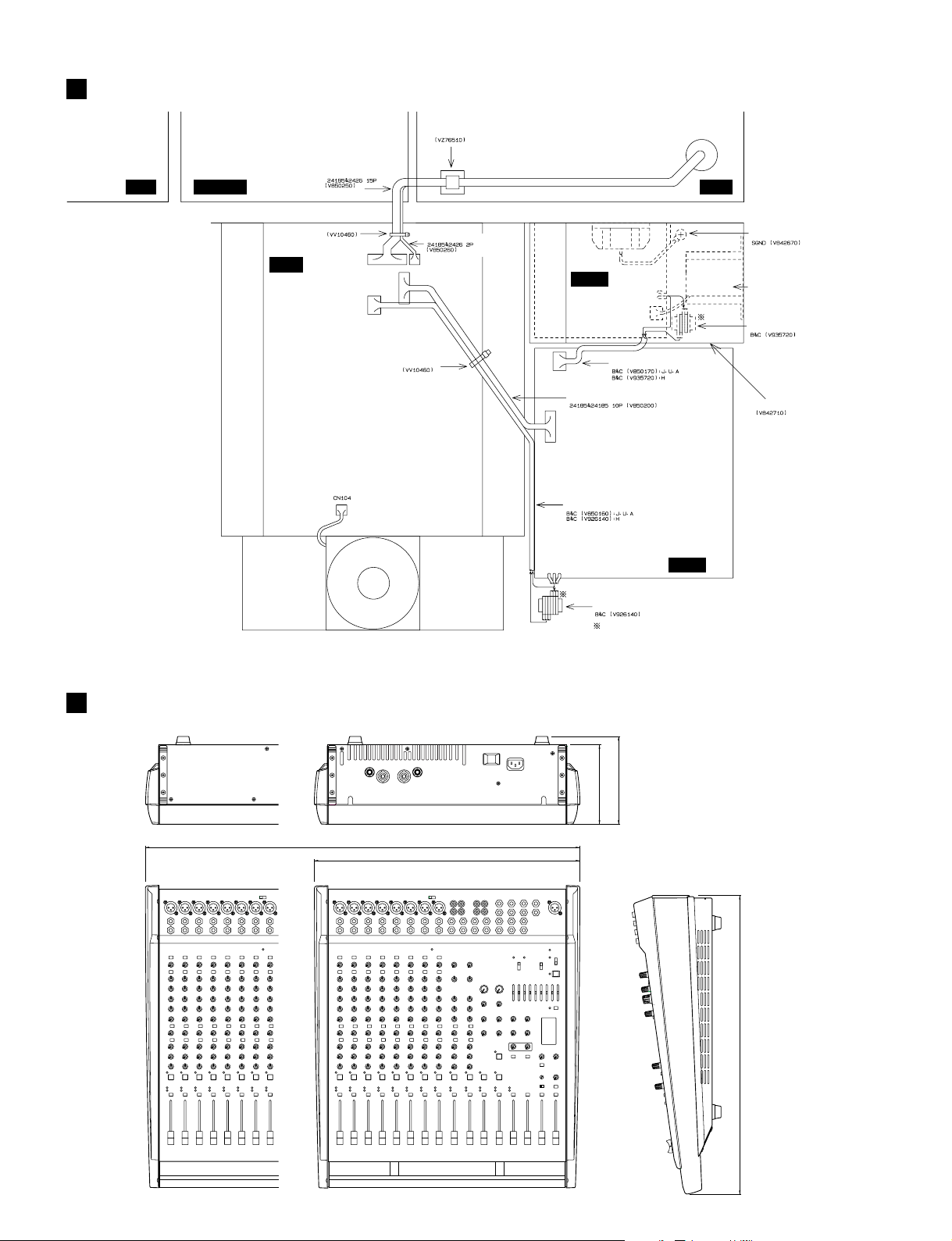
WIRING
IN8
EMX5000-20 only
Cord binder
Connector assembly
IN8/IN16 MAS
Cord holder
PWR
CN101 CN105
CN103
CN102
Connector assembly
CN101
SMPS 1/2
W101
CN102
Connector assembly
Coil
Connector assembly
DIMENSIONS
DC FAN
Cord holder
BOTTOM ASSY
CN103
Connector assembly
CN104
Connector assembly
W102
Connector assembly
Connector assembly
H, B, W, K
158
143
AC shield
SMPS 2/2
14
682 (EMX5000-20)
478 (EMX5000-12)
538
Units: mm
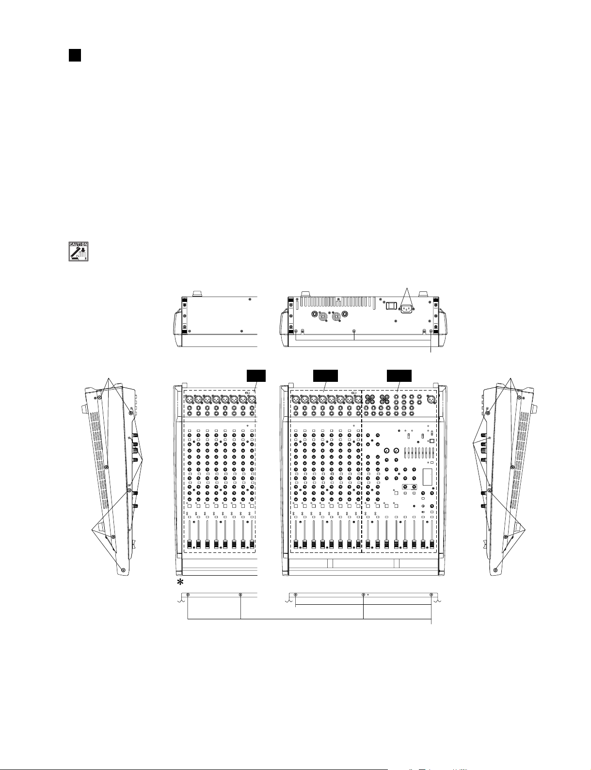
DISASSEMBLY PROCEDURE
1. Panel Assemb ly (Time required: about 5 min utes)
1-1. Remove the six (6) screws marked [30a] and six (6)
screws marked [30b], and then remove the side pads
R and L. (Fig. 1)
1-2. Remove the four (4) screws marked [160a], f our (4)
screws marked [160b], three (3) screws marked
[170a] and four (4) screws marked [170b] (three (3)
for EMX5000-12), Then lift the front end of the panel
assembly, turn it about 45° and remove the panel
assembly by releasing it from the claws on its side .
(Fig. 1)
This mark urges servicemen to pay attention.
EMX5000-12/20
[70]
[30b]
[30b]
[160b]
EMX5000-20 only
IN8 MASIN16
[170b] EMX5000-12
[170a]
[30a]
[160a]
[30a]
[170b] EMX5000-20
[30]: Bind Head Tapping Screw-B 4.0X8 MFZN2BL (EG340190)
[70]: Bind Head Tapping Screw-B 3.0X12 MFZN2BL (VQ074600)
[160]: Bind Head Tapping Screw-B 3.0X6 MFZN2BL (EP600230)
[170]: Bonding Tapping Screw-B 4.0X8 MFZN2BL (VR779900)
Fig.1
15
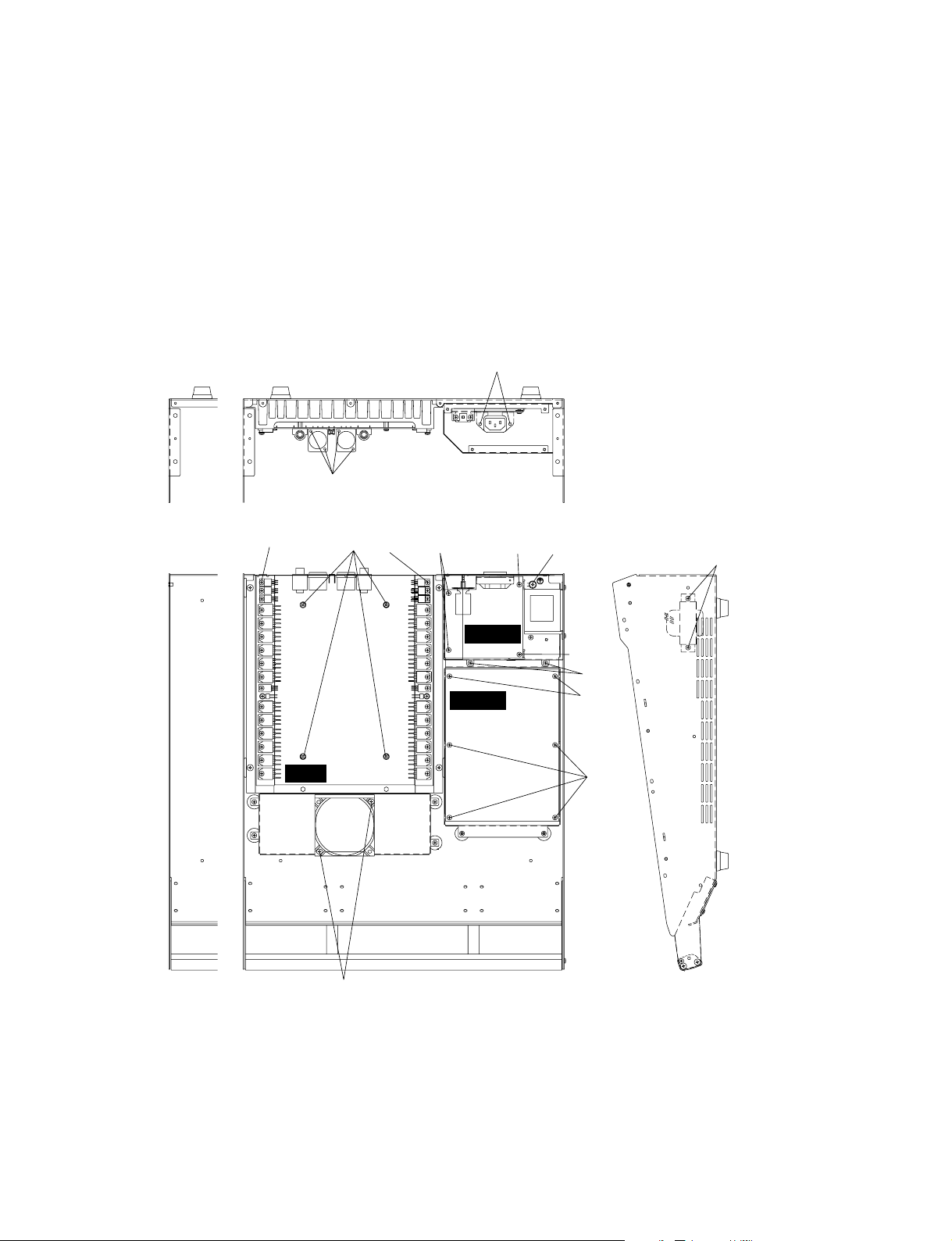
EMX5000-12/20
2. Coil (Time required: about 6 minutes)
2-1. Remove the panel assembly. (See Procedure 1.)
2-2. After removing the two (2) screws marked [B250],
remove the harness and then the coil. (Fig. 2)
3. DC fan (Time required: about 7 minutes)
3-1. Remove the panel assembly. (See Procedure 1.)
3-2. Remove the two (2) screws marked [B120] and
connector. The DC fan can then be remo v ed. (Fig. 2)
[85]
[70]
[B60]
PWR
[B50]
DC Fan
[B120]
[B60]
[B90a]
[B90a]
SMPS 1/2
SMPS 2/2
[B210]
[B250]
[B90a]
[B170]
[B90b]
[B90b]
16
Fig.2
[B50]: Bind Head Screw SP 3.0X8 MFZN2Y (EG330290)
[B60]: Pan Head Screw SPK 3.0X12 MFZN2Y (VJ470900)
[70]: Bind Head Tapping Screw-B 3.0X12 MFZN2BL (VQ074600)
[B90]: Bind Head Tapping Screw-B 3.0X6 MFZN2BL (EP600230)
[B120]: Bind Head Tapping Screw-B 4.0X10 MFZN2BL (EP600240)
[B170]: Bind Head Tapping Screw-B 3.0X6 MFZN2BL (EP600230)
[B210]: Bind Head Screw A4.0X6 MFZN2BL (EG340290)
[B250]: Bind Head Tapping Screw-B 3.0X6 MFZN2BL (EP600230)

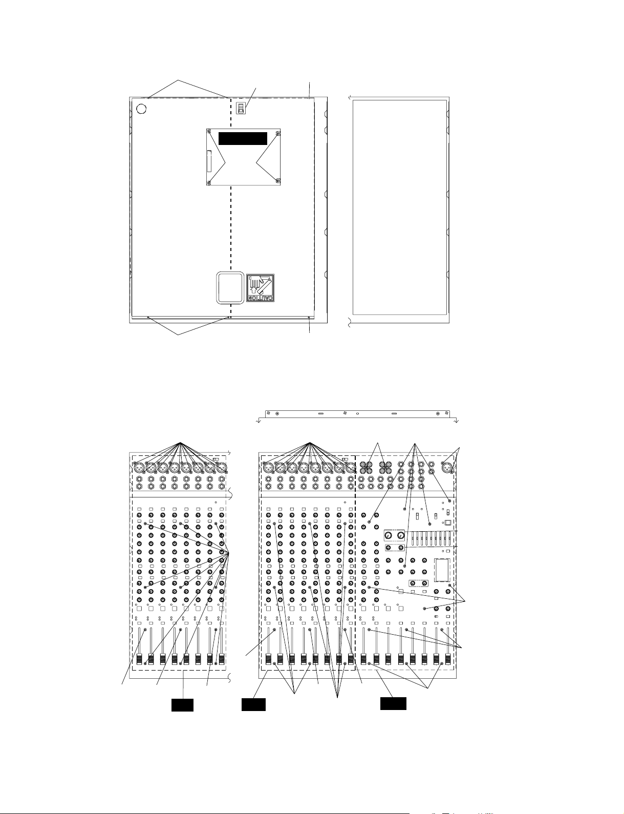
4. DSP Circuit Board
(Time required: about 12 minutes)
4-1. Remove the panel assembly. (See Procedure 1.)
4-2. Remove the four (4) DSP circuit board fixing scre ws
marked [P220], disconnect the card wire connected
to the connector. The DSP circuit board can then be
removed. (Fig. 3)
5. MAS Circuit Board
(Time required: about 30 minutes)
5-1. Remove the panel assembly. (See Procedure 1.)
5-2. Remove the DSP circuit board. (See Procedure 4.)
5-3. Disconnect the two (2) harnesses connected to the
connector assembly fixture marked [P240] on the
main shield plate and remove the six (6) screws
marked [B90]. The main shield plate can then be
removed. (Fig. 3)
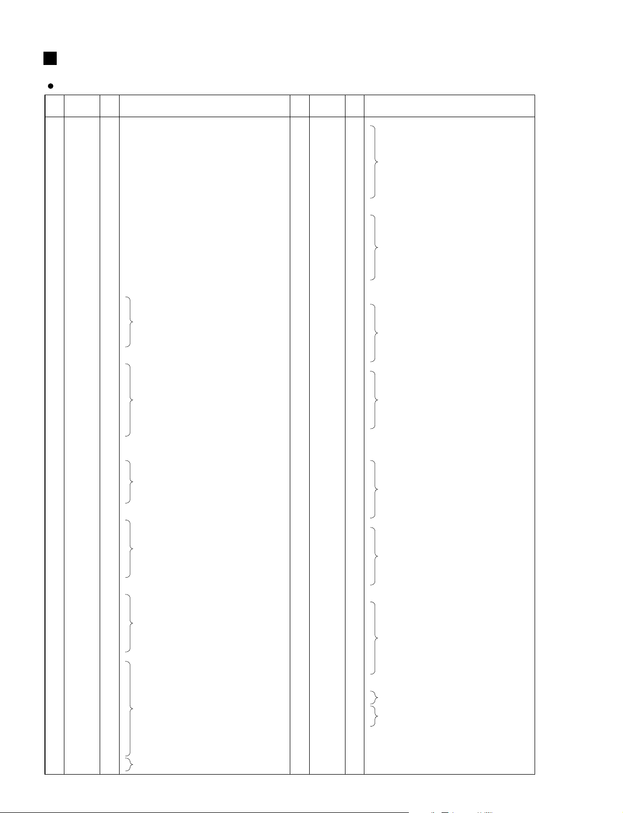
5-4. Remove the two (2) LAMP holder fixing screws
marked [P70a], two (2) pin connector fixing screws
marked [P70b], twenty-two (22) horn connector fixing
hexagonal nuts, knobs (thirty-three (33) big ones, two
(29 small ones and eight (8) fader knobs) and eleven
(11) hexagon socket head scre ws marked [P60a] and
three (3) hexagon socket head screws marked
[P38a]. The MAS circuit board can then be remo v ed.
(Fig. 4)
EMX5000-12/20
6. IN8/IN16 Circuit Boar d: CH1-8 / EMX5000-12, CH918 / EMX5000-20 (Time required: about 40 minutes)
6-1. Remove the panel assembly. (See Procedure 1.)
6-2. Remove the DSP circuit board. (See Procedure 4.)
6-3. Remove the main shield plate. (See Procedure 5-3.)
6-4. Re m ove t h e sixteen (16) cannon connector fixing
screws marked [P70c], sixteen (16) horn connector
fixing hexagonal nuts, knobs (eighty (80) small ones
and eight (8) fader knobs) and nine (9) hexagon
socket head screws marked [P60b] and three (3)
hexagon socket head screws marked [P38b]. The
IN8/IN16 circuit board can then be removed. (Fig. 4)
7. IN8 Circuit Board: CH1-9 / EMX5000-20
(Time required: about 35 minutes)
7-1. Remove the panel assembly. (See Procedure 1.)
7-2. Re m ove t h e sixteen (16) cannon connector fixing
screws marked [P70d], sixteen (16) horn connector
fixing hexagonal nuts, knobs (eighty (80) small ones
and eight (8) fader knobs) and nine (9) hexagon
socket head screws marked [60c] and three (3)
hexagon socket head screws marked [P38c]. The
IN8 circuit board can then be removed. (Fig. 4)
17
EMX5000-12/20
[B90]
[P240]
[B90]
DSP-SPX
[P220]
[B90]
[B90]: Bind Head Tapping Screw-B 3.0X6 MFZN2BL (EP600230)
[B90]
[P70d]
[P60c]
[P38b]
Fig.3
[P70c] [P70b] [P60a]
[P70a]
[P60a]
[P38a]
18
[P38c] [P38c] [P38c]
IN8
[P38]: Screw 3X6 MFZNBL (V9156000)
[P60]: Screw 3X25 MFZNBL (V3289800)
[P70]: Bonding Tapping Screw-B 3.0X8 MFZN2BL (VN413300)
IN16
[P60b]
Fig.4
[P38b]
[P60b]
[P38b]
MAS
[P60a]

8. PWR Circuit Board
(Time required: about 30 minutes)
8-1. Remove the panel assembly. (See Procedure 1.)
8-2. Remove the thirty-four (34) transistor fixing screws
marked [B60], four (4) PWR circuit board fixing
screws marked [B50] from the PWR assembly, four
(4) screws marked [85] and two (2) hexagonal nuts
from the rear panel. The PWR circuit board can then
be removed. (Fig. 2)
9. SMPS 1/2 Circuit Board
(Time required: about 15 minutes)
9-1. Remove the panel assembly. (See Procedure 1.)
9-2. Remove the two (2) AC shield fixing screws mark ed
[B170] and two (2) AC IN socket fixing screws
marked [70] from the rear panel. The AC shield can
then be removed.
9-3. Remove the four (4) SMPS 1/2 circuit board fixing
screws marked [B90a] and one (1) ground cable
fixing screw marked [B210]. (Fig. 2)
9-4. Remove the PSW knob from the rear panel and PSW
escussion (using full care not to break the claw of
the PSW escussion). The SMPS 1/2 circuit board
can then be removed. (Fig. 2)
EMX5000-12/20
10. SMPS 2/2 Circuit Board
(Time required: about 7 minutes)
10-1. Remove the panel assembly. (See Procedure 1.)
10-2. Remove the six (6) SMPS 2/2 circuit board fixing
screws marked [B90b], harness connected to the
PWR circuit board and two (2) harnesses from the
SMPS 1/2 circuit board. The SMPS 2/2 circuit board
can then be removed. (Fig. 2)
19
EMX5000-12/20
LSI PIN DESCRIPTION
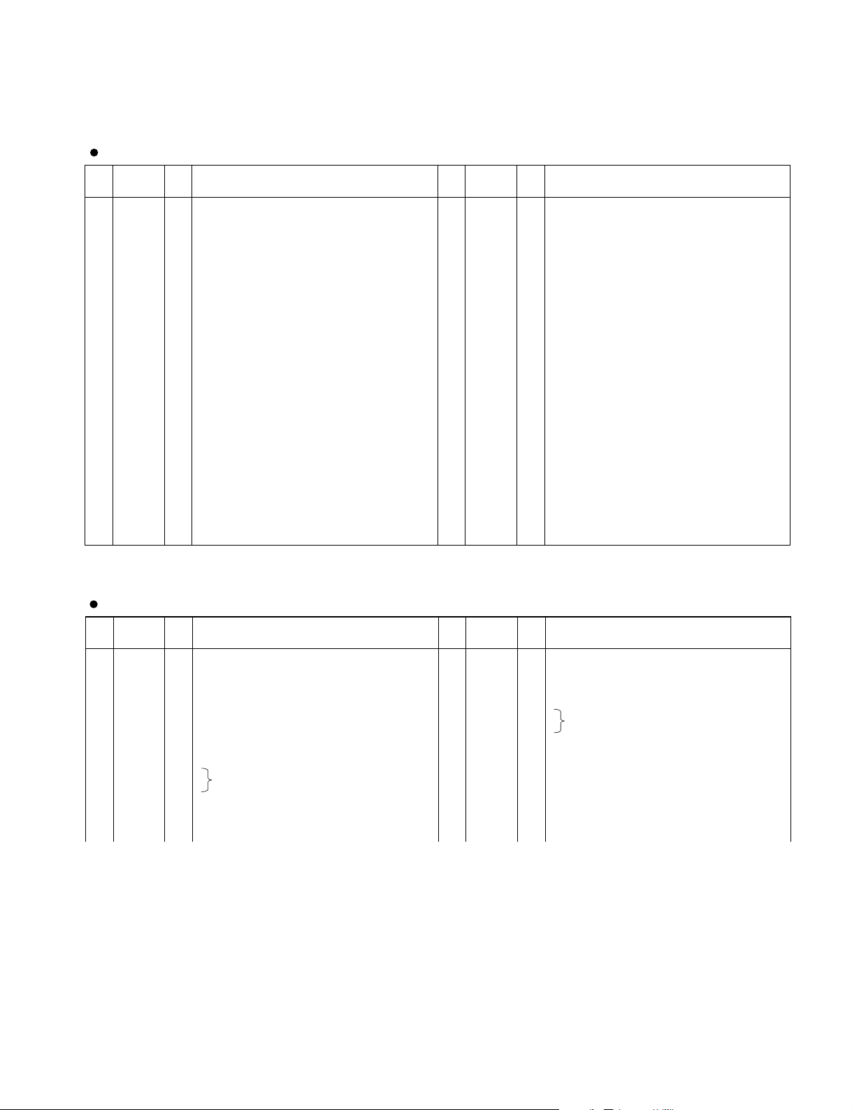
YSS910-S (XV988A00) DSP6 (Digital Signal Processor)
20
PIN
NO.
10
11
12
13
14
15
16
17
18
19
20
21
22
23
24
25
26
27
28
29
30
31
32
33
34
35
36
37
38
39
40
41
42
43
44
45
46
47
48
49
50
51
52
53
54
55
56
57
58
59
60
61
62
63
64
65
66
67
68
69
70
71
72
73
74
75
76
77
78
79
80
81
82
83
84
85
86
87
88
1
2
3
4
5
6
7
8
9
/SYNCI
/SYNCO
CKSEL
MCKS
/SSYNC
/TEST
BTYP
TRIG
CD15
CD14
CD13
CD12
CD11
CD10
CD09
CD08
CD07
CD06
CD05
CD04
CD03
CD02
CD01
CD00
/WAIT
DB00
DB01
DB02
DB03
DB04
DB05
DB06
DB07
DB08
DB09
DB10
DB11
DB12
Vdd
Vss
XI
XO
Vdd
Vdd
CKI
CKO
Vss
/IC
/IRQ
Vdd
Vss
/CS
/WR
/RD
CA7
CA6
CA5
CA4
CA3
CA2
CA1
Vss
Vdd
Vss
Vdd
Vdd
Vss
SI0
SI1
SI2
SI3
SI4
SI5
SI6
SI7
Vss
Vdd
SO0
SO1
SO2
SO3
SO4
SO5
SO6
SO7
Vss
Vdd
Vdd
I/O FUNCTIONNAME
I/O
I/O
I/O
I/O
I/O
I/O
I/O
I/O
I/O
I/O
I/O
I/O
I/O
I/O
I/O
I/O
I/O
I/O
I/O
I/O
I/O
I/O
I/O
I/O
I/O
I/O
I/O
I/O
I/O
I/O
I/O
I/O
I/O
I/O
I/O
I/O
I/O
Power supply (3.3 V)
Ground
System master clock input (60 MHz or 30 MHz)
I
O
O
O
O
O
O
O
O
O
O
O
O
O
System master clock output (High or 30 MHz)
Power supply (5 V)
Sync. signal input
I
Sync. signal output
Power supply (5 V)
System clock input (30 MHz)
I
System clock output (30 MHz)
System master clock select (0: 60 MHz, 1: 30 MHz)
I
Ground
Serial I/O master clock input (128 x Fs)
I
Serial I/O Sync. signal output
I
Initial clear
I
Test mode setting (0: Test, 1: Normal)
I
Data bus type select (0: 8 bit, 1: 16 bit)
I
IRQ output
Trigger signal input/output
Power supply (5 V)
Ground
chip select signal input
I
Write signal input
I
Read signal input
I
Address bus of internal register
Ground
Power supply (3.3 V)
Data bus of internal register
Ground
Power supply (3.3 V)
Power supply (5 V)
Data bus of internal register
WAIT output
Ground
I
I
I
I
Serial data input
I
I
I
I
Ground
Power supply (5 V)
Serial data output
Ground
Parallel data bus
Power supply (5 V)
Power supply (3.3 V)
PIN
NO.
100
101
102
103
104
105
106
107
108
109
110
111
112
113
114
115
116
117
118
119
120
121
122
123
124
125
126
127
128
129
130
131
132
133
134
135
136
137
138
139
140
141
142
143
144
145
146
147
148
149
150
151
152
153
154
155
156
157
158
159
160
161
162
163
164
165
166
167
168
169
170
171
172
173
174
175
176
89
90
91
92
93
94
95
96
97
98
99
Vss
DB13
DB14
DB15
DB16
DB17
DB18
DB19
DB20
DB21
DB22
Vss
Vdd
DB23
DB24
DB25
DB26
DB27
DB28
DB29
DB30
DB31
TIMO/DBOB
Vss
Vdd
DA00
DA01
DA02
DA03
DA04
DA05
DA06
DA07
Vss
DA08
DA09
DA10
DA11
DA12
DA13
DA14
DA15
Vss
Vdd
(n.c)
Vdd
DA16
DA17
DA18
DA19
DA20
DA21
DA22
DA23
Vss
DA24
DA25
DA26
DA27
DA28
DA29
DA30
DA31
Vdd
Vss
A00
A01
A02
A03
A04
A05
A06
A07
A08
A09
Vss
Vdd
A10
A11
A12
A13
A14
A15/RAS
A16/CAS
A17/CE
/WE
/OE
Vdd
I/O FUNCTIONNAME
I/O
I/O
I/O
I/O
I/O
I/O
I/O
I/O
I/O
I/O
I/O
I/O
I/O
I/O
I/O
I/O
I/O
I/O
I/O
I/O
I/O
I/O
I/O
I/O
I/O
I/O
I/O
I/O
I/O
I/O
I/O
I/O
I/O
I/O
I/O
I/O
I/O
I/O
I/O
I/O
I/O
I/O
I/O
I/O
I/O
I/O
I/O
I/O
I/O
I/O
I/O
I/O
DSP-SPX: IC112
Ground
Parallel data bus
Ground
Power supply (3.3 V)
Parallel data bus
Timing signal output/ Parallel data bus output/ input
Ground
Power supply (5 V)
Memory data bus
Ground
Memory data bus
Ground
Power supply (3.3 V)
Not used
Power supply (5 V)
Memory data bus
Ground
Memory data bus
Power supply (5 V)
O
O
O
O
O
O
O
O
O
O
O
O
O
O
O
O
O
O
O
O
Ground
Memory address (SRAM, PSRAM, DRAM)
Ground
Power supply (3.3 V)
Memory address (SRAM, PSRAM, DRAM)
Memory address (SRAM, PSRAM)
Memory address (SRAM, PSRAM), /RAS (DRAM)
Memory address (SRAM, PSRAM), /CAS (DRAM)
Memory address (SRAM), /CE (PSRAM)
Memory write enable signal
Memory output enable signal
Power supply (5 V)
EMX5000-12/20
YM3436DK (XG948E0) DIR2 (Digital Format Interface Receiver)
PIN
NO.
10
11
12
13
14
15
16
17
18
19
20
21
22
1
2
3
4
5
6
7
8
9
DAUX
HDLT
DOUT
VFL
OPT
SYNC
MCC
WC
MCB
MCA
SKSY
XI
XO
P256
LOCK
Vss
TC
DIM1
DIM0
DOM1
DOM0
KM1
I/O FUNCTIONNAME
I
O
O
O
O
O
O
O
O
O
I
I
O
O
O
O
I
I
I
I
I
Auxiliary input for audio data
Asynchronous buffer operation flag
Audio data output
Parity flag output
Fs x 1 Synchronous output signal for DAC
Fs x 1 Synchronous output signal for DSP
Fs x 64 Bit clock output
Fs x 1 Word clock output
Fs x 128 Bit clock output
Fs x 256 Bit clock output
Clock synchronization control input
Crystal oscillator connection or external
clock input
Crystal oscillator connection
VCO oscillating clock connection
PLL lock flag
Logic section power (GND)
PLL time constant switching output
Data input mode selection
Data input mode selection
Data output mode selection
Data output mode selection
Clock mode switching input 1
PIN
NO.
23
24
25
26
27
28
29
30
31
32
33
34
35
36
37
38
39
40
41
42
43
44
RSTN
Vdda
CTLN
PCO
(NC)
CTLP
Vssa
TSTN
KM2
KM0
FS1
FS0
CSM
EXTW
DDIN
LR
Vdd
ERR
EMP
CD0
CCK
CLD
I/O FUNCTIONNAME
I
I
O
I
I
I
I
O
O
I
I
I
O
O
O
O
I
I
DSP-SPX: IC103
System reset input
VCO section power (+5V)
VCO control input N
PLL phase comparison output
VCO control input P
VCO section power (GND)
Test terminal. Open for normal use
Clock mode switching input 2
Clock mode switching input 0
Channel status sampling frequency
display output 1
Channel status sampling frequency
display output 0
Channel status output method selection
External synchronous auxiliary input
word clock
EIAJ (AES/EBU) data input
PLL word clock output
Logic section power (+5 V)
Data error flag output
Channel status emphasis control code
output
3-wire type microcomputer interface data
output
3-wire type microcomputer interface clock
input
3-wire type microcomputer interface load
input
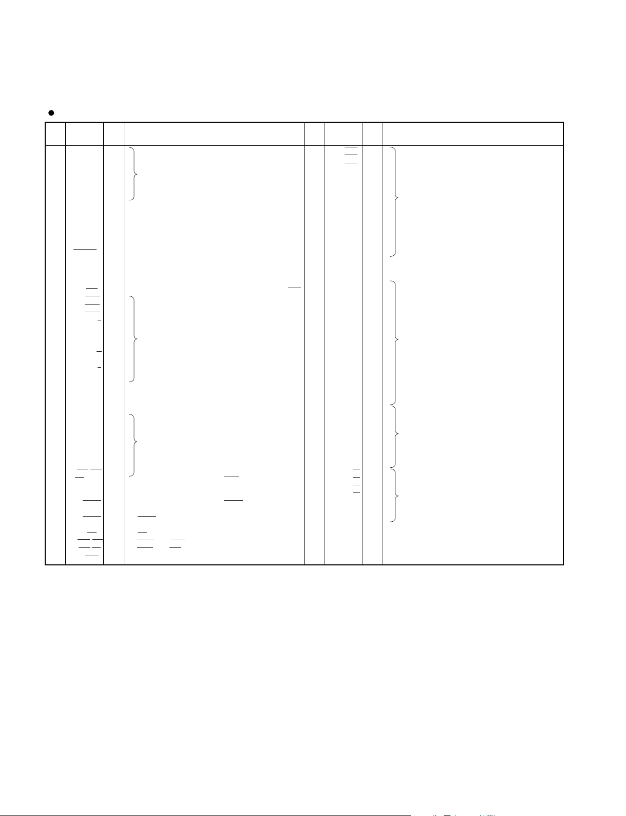
AK4522VF-E2 (XW008A00) CODEC (CMOS A/D & D/A Converter)
PIN
NO.
10
11
12
1
2
3
4
5
6
7
8
9
VREFH
AINR+
AINRAINL+
AINL-
VA
AGND
DIF0
DIF1
LRCK
SCLK
SDTI
I/O FUNCTIONNAME
I
I
I
I
I
-
I
I
I
I
I
Positive voltage reference input , VA
Used as a positive voltage reference by
ADC & DAC, VREFH is conne externally
to filtered VA.
Rch analog positive input
Rch analog negative input
Lch analog positive input
Lch analog negative input
Analog power supply
Analog ground
Audio data interface format
Input/Output channel clock
Audio serial data clock
Audio serial data input
PIN
NO.
13
14
15
16
17
18
19
20
21
22
23
24
SDTO
SMUTE
DEM0
DEM1
MCKI
VD
DGND
/PD
CMODE
AOUTL
AOUTR
VCOM
I/O FUNCTIONNAME
O
I
I
I
I
-
I
I
O
O
O
DSP-SPX: IC108, IC308
Audio serial data output
Soft mute
When this pin goes "H", soft mute cycle
is intiated.
When returning "L", the output mute releases.
De-emphasis frequency select
Master clock Input/X'tal input
Digital power supply
Digital ground
Reset
Master clock select (Internal biased pin)
"H": 384fs, "L": 256fs, "NS": 512fs
Lch analog output
Rch analog output
Common voltage output , VA/2
21
EMX5000-12/20
M30622MCA-XXXFP (X2416A00) CPU
PIN
NO.
P96/
1
P95/
2
P94/
3
P93/
4
P92/
5
P91/
6
P90/
7
BYTE
8
CNVss
9
P87/XCIN
10
P86/XCOUT
11
RESET
12
XOUT
13
14
15
16
P85/NMI
17
P84/INT2
18
P83/INT1
19
P82/INT0
20
P81/TA4IN/U
21
P80/TA4IN/U
22
P77/TA3IN
23
P76/TA3OUT
24
P75/TA2IN/W
25
P74/TA2OUT/W
26
P73/TA1IN/V
27
P72/CLK2/TA1OUT
28
P71/RxD2
29
P70/TxD2
30
P67/TxD1
31
P66/RxD1
32
P65/CLK1
33
P64/RTS1
34
P63/TxD0
35
P62/RxD0
36
P61/CLK0
37
P60/CTS0/RTS0
38
P57/RDY/CLKOUT
39
P56/ALE
40
P55/HOLD
41
P54/HLDA
42
P53/BCLK
43
P52/RD
44
P51/WRH/BHE
45
P50/WRL/WR
46
P47/CS3
47
Vss
XIN
Vcc
I/O FUNCTIONNAME
I/O
I/O
I/O
I/O
I/O
I/O
I/O
I
I
I/O
I/O
I
O
I
I
I/O
I/O
I/O
I/O
I/O
I/O
I/O
I/O
I/O
I/O
I/O
I/O
I/O
I/O
I/O
I/O
I/O
I/O
I/O
I/O
I/O
I
O
I
O
O
O
O
O
I/O/O
This is an 8-bits I/O port.
External data bus width select input.
CNVss
This is set using software to function as the I/O
pins fpr a sub clock generation circuit.
This is set using software to function as the I/O
pins fpr a sub clock generation circuit.
A "L" on this input resets the microcomputer.
Clock output
Power supply 0V.
Clock input
Power supply 2.7V to 5.5V.
This is an input-only port that also functions for NMI.
This is an 8-bits I/O port.
This is an 8-bits I/O port.
This is N channel open-drain output.
This is an 8-bits I/O port. This is N channel
open-drain output.
This is an 8-bits I/O port.
While the input level at the RDY pin is "L",
the microcomputer is in the ready state.
ALE output signal
While the input level at the HOLD pin is "L",
the microcomputer is placed in the hold state.
HLDA output signal
BCLK output signal
RD output signal
WRH and BHE output signals
WRL and WR output signals
This is an 8-bits I/O port.
PIN
NO.
P46/CS2
48
P45/CS1
49
P44/CS0
50
P43/A19
51
P42/A18
52
P41/A17
53
P40/A16
54
P37/A15
55
P36/A14
56
P35/A13
57
P34/A12
58
P33/A11
59
P32/A10
60
61
62
P30/A8(/-/D7)
63
64
P27/A7(/D7/D6)
65
P26/A6(/D6/D5)
66
P25/A5(/D5/D4)
67
P24/A4(/D4/D3)
68
P23/A3(/D3/D2)
69
P22/A2(/D2/D1)
70
P21/A1(/D1/D0)
71
P20/A0(/D0/-)
72
P17/D15
73
P16/D14
74
P15/D13
75
P14/D12
76
P13/D11
77
P12/D10
78
79
80
81
82
83
84
85
86
87
88
P107/AN7/KI3
89
P106/AN6/KI2
90
P105/AN5/KI1
91
P104/AN4/KI0
92
P103/AN3
93
P102/AN2
94
P101/AN1
95
96
P100/AN0
97
98
99
P97/TRG
100
P31/A9
Vcc
Vss
P11/D9
P10/D8
P07/D7
P06/D6
P05/D5
P04/D4
P03/D3
P02/D2
P01/D1
P00/D0
Avss
VREF
Avcc
I/O FUNCTIONNAME
I/O/O
I/O/O
I/O/O
I/O/O
I/O/O
I/O/O
I/O/O
I/O/O
I/O/O
I/O/O
I/O/O
I/O/O
I/O/O
I/O/O
I/O/O
I/O/O
I/O/O
I/O/O
I/O/O
I/O/O
I/O/O
I/O/O
I/O/O
I/O
I/O
I/O
I/O
I/O
I/O
I/O
I/O
I/O
I/O
I/O
I/O
I/O
I/O
I/O
I/O
I/O
I/O
I/O
I/O
I/O
I/O
I/O
I/O
I
I/O
This is an 8-bits I/O port.
Power supply 2.7V to 5.5V.
This is an 8-bits I/O port.
Power supply 0V.
This is an 8-bits I/O port.
This is an 8-bits CMOS I/O port.
This is an 8-bits I/O port.
Analog power supply input
This is an 8-bits I/O port.
Reference voltage input
Analog power supply input
This is an 8-bits I/O port.
DSP-SPX: IC109
22
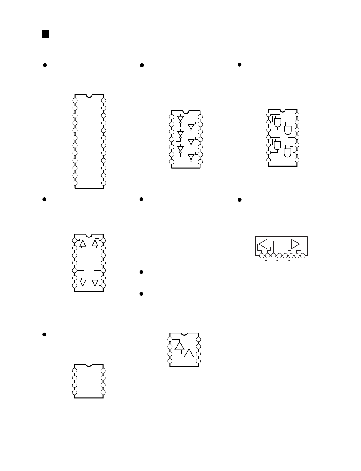
IC BLOCK DIAGRAM
EMX5000-12/20
LB1412M (XT547A00)
LED DRIVER
MAS: IC601, IC602
NC
24
D7
23
D6
22
D5
21
D4
20
D3
19
D2
18
17
D1
16
V
CC
15
I
LED
14
OSC
13
V
Z
GND
OUT1
OUT2
RESET
1NC
D8
2
D9
3
D10
4
5
D11
6
D12
7
8
IN1
9
10
IN2
11
12
NJM2060(TE2) (XM560A00)
OP AMP
MAS: IC311-315
D OUTPUT
14
+
D –INPUT
13
D +INLPUT
12
V–
11
C +INPUT
10
C –INPUT
9
+
–
C
C OUTPUT
8
A –INPUT
A +INPUT
B +INPUT
B –INPUT
B OUTPUT
V+
1A OUTPUT
AD
+
––
2
3
4
5
6
+
–
B
7
74HCU04DT (XZ110A00)
INVERTER
DSP-SPX: IC104
11A
2
1Y
3
2A
4
2Y
5
3A
6
3Y
7
SS
V
NJM2068MD-T1
(XJ553A00)
DD
V
14
6A
13
6Y
12
5A
11
5Y
10
4A
9
4Y
8
OP AMP
IN8: IC101-105,IC107, IC201, IC301-305,
IC307, IC401, IC501-505, IC507,
IC601, IC701-705, IC707, IC801
DSP-SPX: IC105-107, IC305-307
MAS: IC101-104, IC201-204, IC301-310,
IC318, IC501-504, IC603, IC701, IC702
20ch only
IN16: IC101-105, IC107, IC201, IC301-305,
IC307, IC401, IC501-505, IC507,
IC601, IC701-705, IC707, IC801
NJM4580ED
(XT157A00)
OP AMP
MAS: IC316, IC317, IC319-321
NJM4588M(T1)
(IG103520)
OP AMP
IN8: IC106, IC306, IC506, IC706
MAS: IC105, IC605, IC606
20ch only
IN16: IC106, IC306, IC506, IC706
74HC08DT(XZ108A00)
AND
DSP-SPX: IC111
1
2
1B
1Y
3
2Y
4
2A
5
2B
6
Vss
7
141A
VDD
13
4B
12
4A
11
4Y
10
3Y
9
3A
8
3B
NJM4556AL(XP844A00
OP AMP
MAS: IC505
+
1A2 3 4 5 6 7 8
IN V
+
IN
OUT
AAA
+
+
IN
BBB
B
OUT
+
VIN
)
IR2153 (X2264A00)
CONTROL IC
SMPS1/2,2/2: IC102
Vcc
1
R
2
T
C
3
T
4
COM
+-
8
7
6
5
+DC Voltage
Supply
Output B
Inverting
Input B
Non-Inverting
Input B
1
Output A
Inverting
2
Input A
Non-Inverting
Input A
Ground
V
B
8
HO
7
V
6
S
5
LO
+-
3
4
23
24
CN903
CN904
CN901
CN902
INPUT A
INPUT B
Location No.
INSERT
Model
1/9
INPUT
2/10 3/11 4/12 5/13 6/14 7/15 8/16
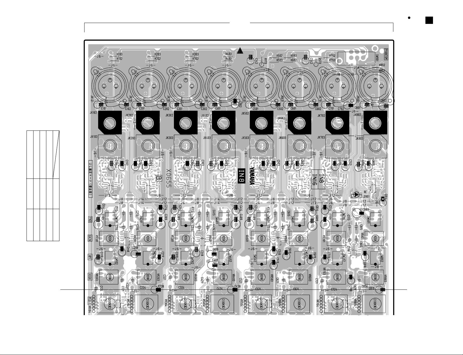
IN8/IN16 Circuit Board
EMX5000-12/20
CIRCUIT BOARDS
install
install
install
IN8/IN16: 3NA-V826740
IN16
not install
not install
IN8
A
PAD
GAIN
HPF
HIGH
MID-f
install
install
install
PHANTOM
A
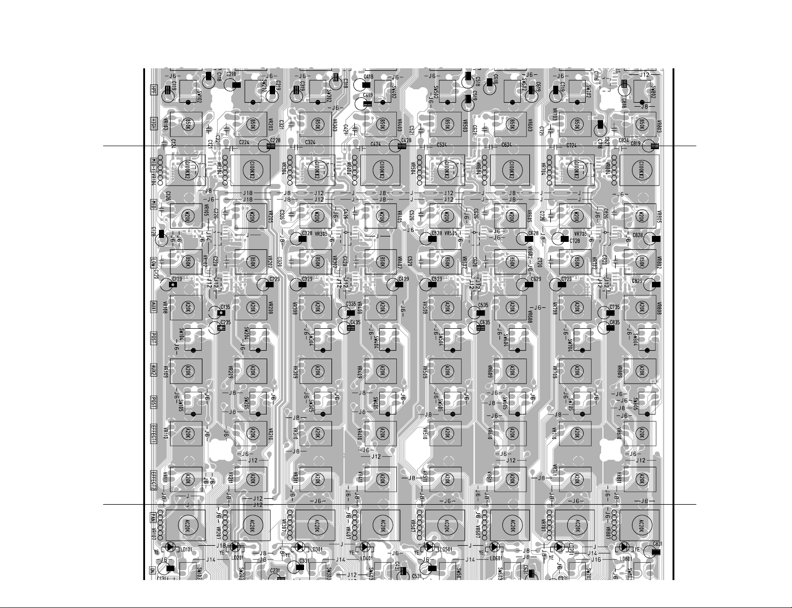
IN8/IN16: 3NA-V826740
HPF
HIGH
A
MID-f
MID
LOW
AUX1
POST
A
25
AUX2
POST
EFFECT1
EFFECT2
B
CH
ON/OFF
PAN
B
EMX5000-12/20
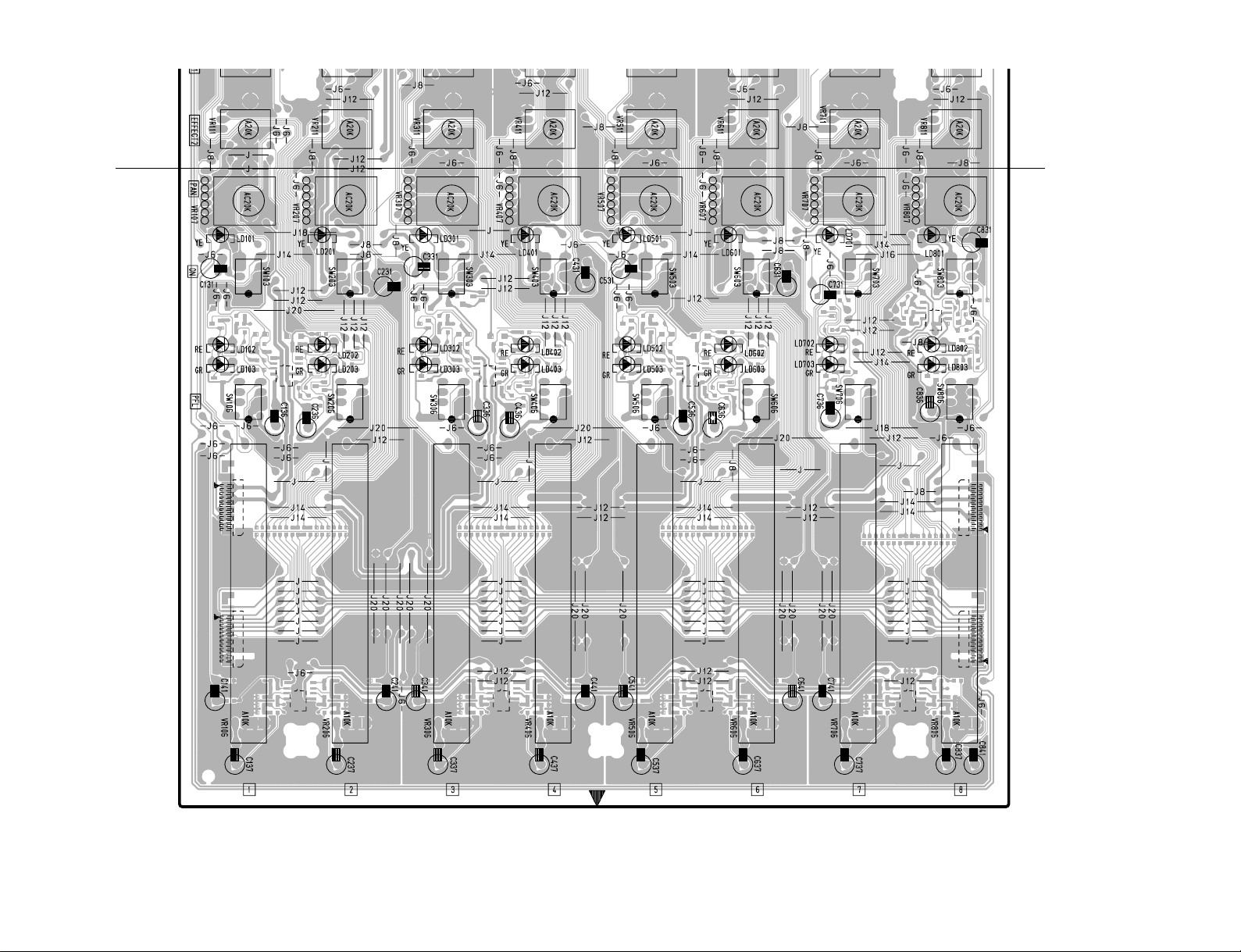
26
EFFECT2
B
CH
ON/OFF
PEAK
SIGNAL
EMX5000-12/20
B
PAN
PFL
CN902:
(EMX5000-20)
from IN8
(EMX5000-12)
N.C.
FADER
CN901:
(EMX5000-26)
from IN8
Component side
(EMX5000-12)
N.C.
IN8/IN16: 3NA-V826740
CN902CN901
CN904:
(EMX5000-20)
to othere IN8 CN902
or MAS CN604
(EMX5000-12)
to MAS CN604
CN903:
(EMX5000-20)
to othere IN8 CN901
CN903 CN904
or MAS CN603
(EMX5000-12)
to MAS CN603
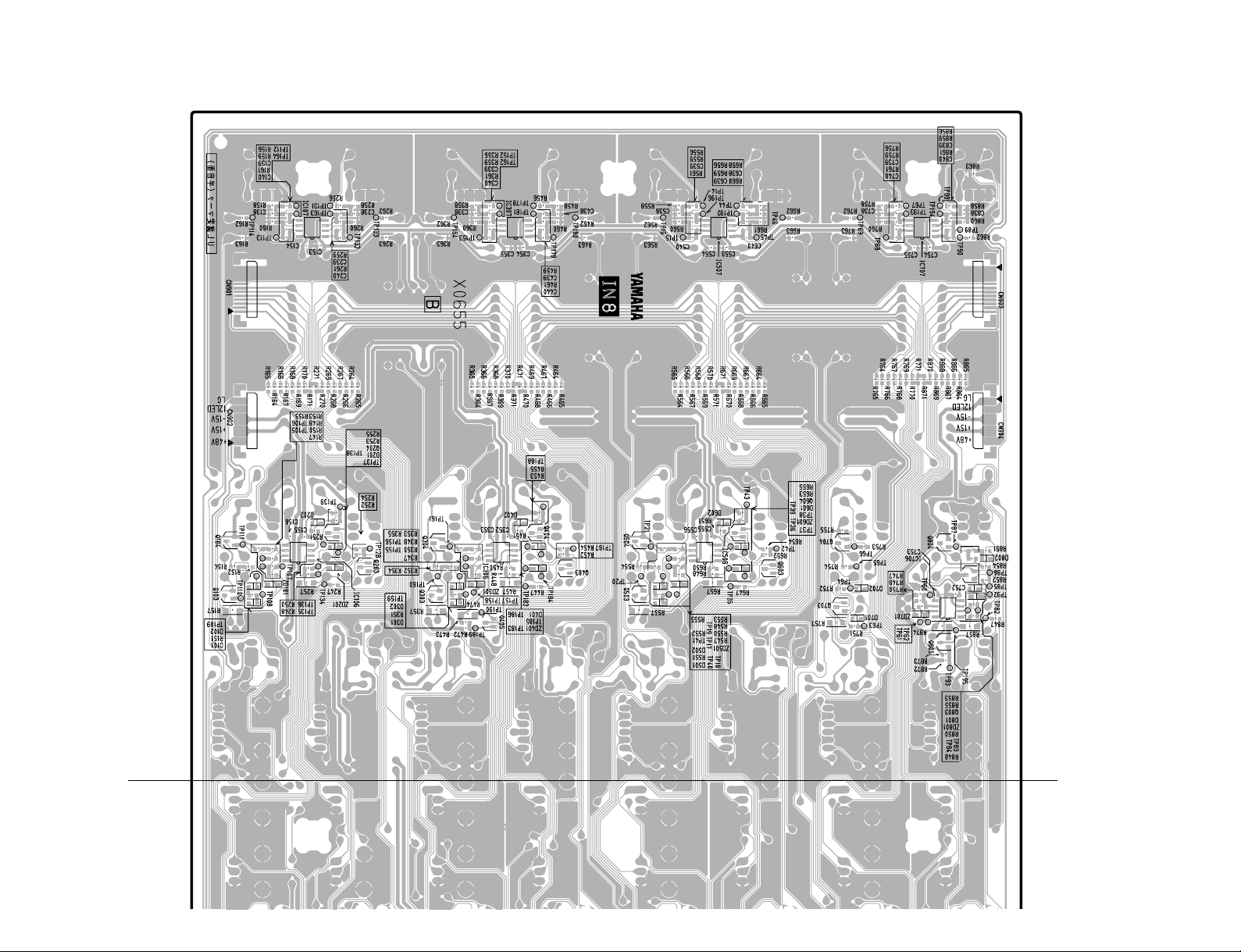
IN8/IN16: 3NA-V826740
27
A
A
EMX5000-12/20
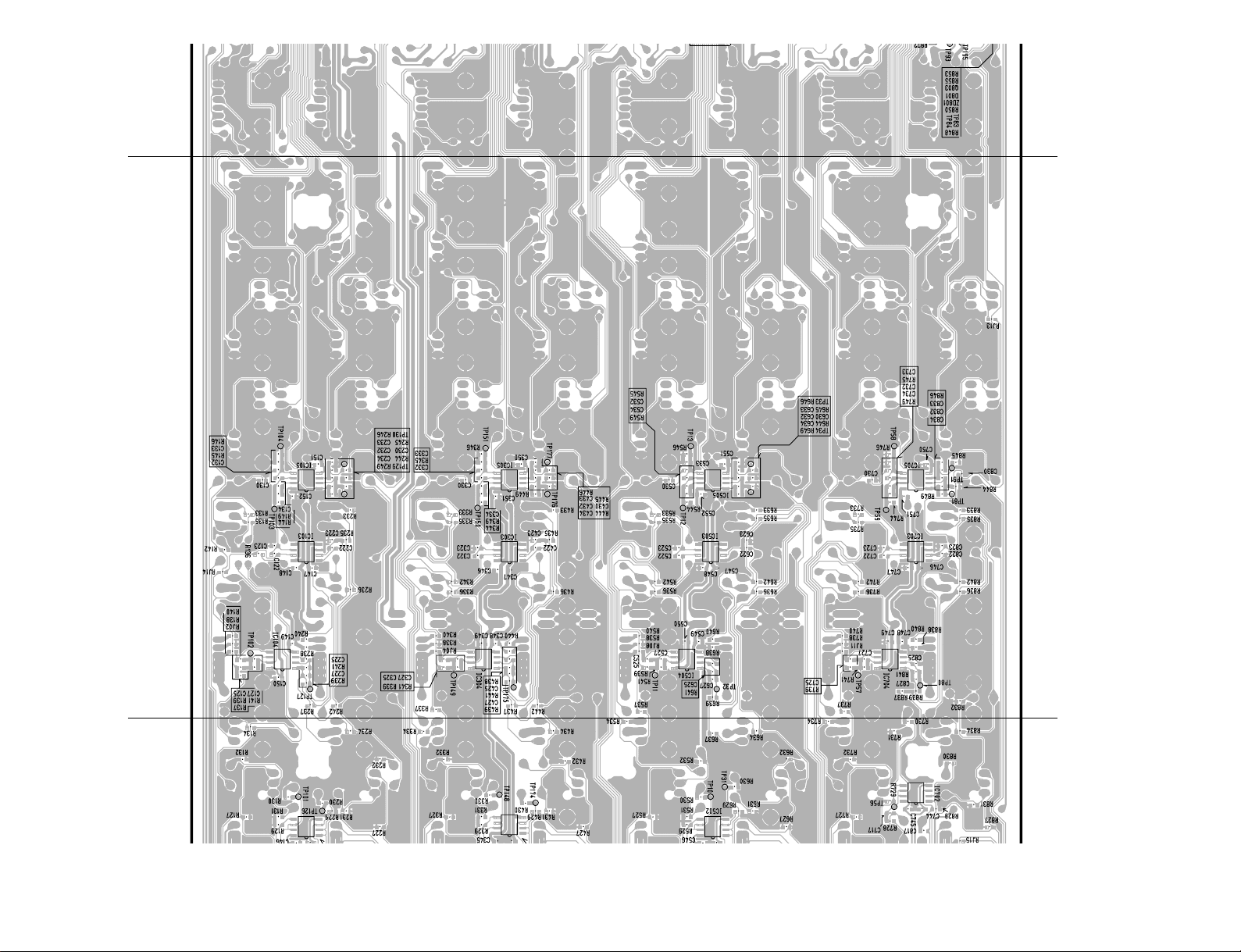
28
EMX5000-12/20
A
A
IN8/IN16: 3NA-V826740
B
B
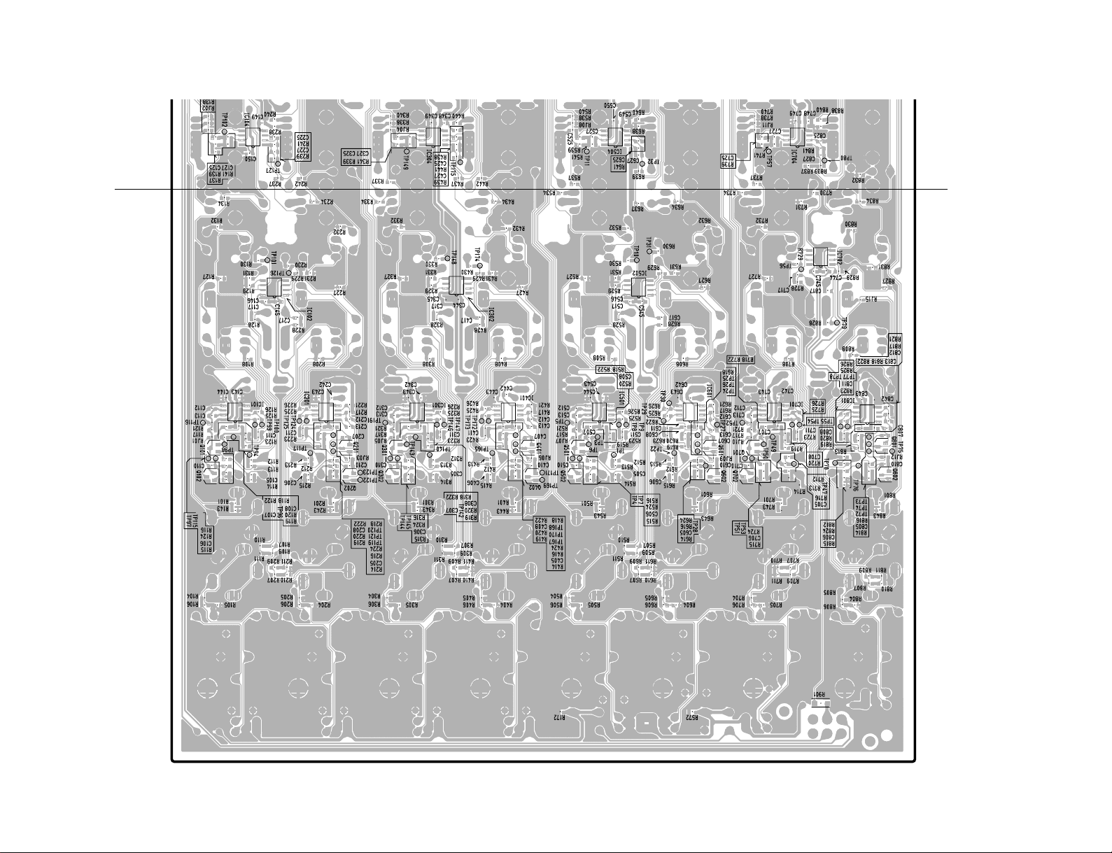
IN8/IN16: 3NA-V826740
B
B
Pattern side
29
EMX5000-12/20
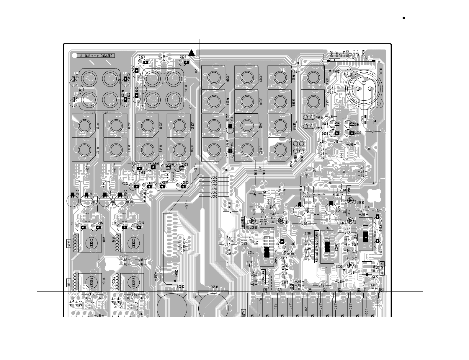
30
CN501:
to DSP
CN601:
to PWR CN101
MAS Circuit Board
EMX5000-12/20
LINE17 L LINE19 L
LINE18 R
17 L 19 L
18 R 20 R
LINE20 R 2TR IN R REC OUT R
2TR IN L REC OUT L
ST SUB IN1 L ST SUB IN2 L
ST SUB IN1 R ST SUB IN2 R
AUX SEND1
AUX SEND2
EFFECT SEND1
EFFECT SEND2
ST OUT L
ST OUT R
R AMP IN A
R AMP IN B
LIMITER
ST SUB L
ST SUB R
MONO OUT
PHONES
AMP MODE
EFFECT ON/OFF
TAP
LAMP
CN602:
to PWR CN105
POWER
YSP
GAIN
MAS: 3NA-V826750
HIGH
A
PROGRAM
POWER 500W/
300W/100W
STAND-BY
A
 Loading...