

Page 1
DVD PLAYER
DVD-S661/DV-S6160
SERVICE MANUAL
SERVICE MANUAL
SERVICE MANUAL
For U, K, A, L, P models
This service manual is for the DVD-S661/DV-S6160 (U, K, A, L, P models).
For the DVD-S661 (G model) service manual, please refer to the following service manual:
DVD-S661 (G model): 101047
IMPORTANT NOTICE
This manual has been provided for the use of authorized YAMAHA Retailers and their service personnel.
It has been assumed that basic service procedures inherent to the industry, and more specifically YAMAHA Products, are already
known and understood by the users, and have therefore not been restated.
WARNING: Failure to follow appropriate service and safety procedures when servicing this product may result in personal
IMPORTANT: The presentation or sale of this manual to any individual or firm does not constitute authorization, certification or
The data provided is believed to be accurate and applicable to the unit(s) indicated on the cover. The research, engineering, and
service departments of YAMAHA are continually striving to improve YAMAHA products. Modifications are, therefore, inevitable
and specifications are subject to change without notice or obligation to retrofit. Should any discrepancy appear to exist, please
contact the distributor's Service Division.
WARNING: Static discharges can destroy expensive components. Discharge any static electricity your body may have
IMPORTANT: Turn the unit OFF during disassembly and part replacement. Recheck all work before you apply power to the unit.
injury, destruction of expensive components, and failure of the product to perform as specified. For these reasons,
we advise all YAMAHA product owners that any service required should be performed by an authorized
YAMAHA Retailer or the appointed service representative.
recognition of any applicable technical capabilities, or establish a principle-agent relationship of any form.
accumulated by grounding yourself to the ground buss in the unit (heavy gauge black wires connect to this buss).
■ CONTENTS
TO SERVICE PERSONNEL ...................................... 2–3
PREVENTION OF ELECTROSTATIC DISCHARGE .... 4
LOCALE MANAGEMENT INFORMATION ................... 4
FRONT PANELS ............................................................ 5
REAR PANELS ........................................................... 5-6
REMOTE CONTROL PANEL ........................................ 6
SPECIFICATIONS...................................................... 6–7
INTERNAL VIEW ........................................................... 8
REPAIR NOTES ............................................................. 9
TRADE MODE ................................................................ 9
101050
2007 All rights reserved.
This manual is copyrighted by YAMAHA and may not be copied or
redistributed either in print or electronically without permission.
DISASSEMBLY PROCEDURES ................................. 10
TEST MODE ................................................................. 11
BLOCK DIAGRAM ....................................................... 12
WIRING DIAGRAM ...................................................... 13
PRINTED CIRCUIT BOARDS................................ 14–19
SCHEMATIC DIAGRAMS ...................................... 20–26
REPLACEMENT PARTS LIST .............................. 28–29
REMOTE CONTROL.................................................... 29
SCENE CONTROL ....................................................... 30
P.O.Box 1, Hamamatsu, Japan
'07.05
DVD-S661/
DV-S6160
Page 2

DVD-S661/DV-S6160
■ TO SERVICE PERSONNEL
1. Critical Components Information
Components having special characteristics are marked Z
and must be replaced with parts having specifications equal
to those originally installed.
2. Leakage Current Measurement (For 120V Models Only)
When service has been completed, it is imperative to verify
that all exposed conductive surfaces are properly insulated
from supply circuits.
● Meter impedance should be equivalent to 1500 ohms shunted
by 0.15µF.
WALL
OUTLET
● Leakage current must not exceed 0.5mA.
● Be sure to test for leakage with the AC plug in both polari-
ties.
EQUIPMENT
UNDER TEST
INSULATING
TABLE
AC LEAKAGE
TESTER OR
EQUIVALENT
WARNING: CHEMICAL CONTENT NOTICE!
The solder used in the production of this product contains LEAD. In addition, other electrical/electronic and/or plastic
(where applicable) components may also contain traces of chemicals found by the California Health and Welfare
Agency (and possibly other entities) to cause cancer and/or birth defects or other reproductive harm.
DO NOT PLACE SOLDER, ELECTRICAL/ELECTRONIC OR PLASTIC COMPONENTS IN YOUR MOUTH FOR ANY
REASON WHATSOEVER!
Avoid prolonged, unprotected contact between solder and your skin! When soldering, do not inhale solder fumes or
expose eyes to solder/flux vapor!
If you come in contact with solder or components located inside the enclosure of this product, wash your hands
before handling food.
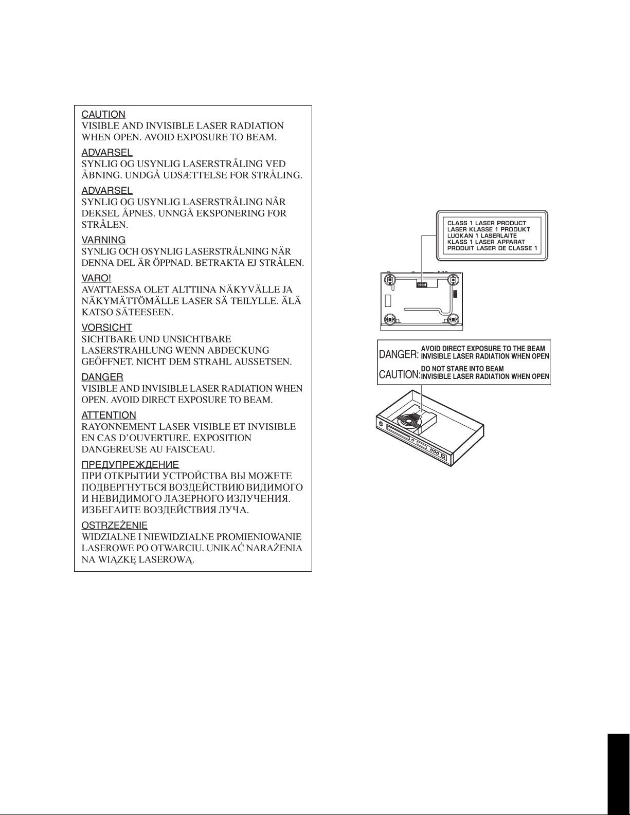
WARNING: Laser Safety
This product contains a laser beam component. This component may emit invisible, as well as visible radiation,
which may cause eye damage. To protect your eyes and skin from laser radiation, the following precautions must be
used during servicing of the unit.
1) When testing and/or repairing any component within the product, keep your eyes and skin more than 30 cm away from
the laser pick-up unit at all times. Do not stare at the laser beam at any time.
2) Do not attempt to readjust, disassemble or repair the laser pick-up, unless noted elsewhere in this manual.
3) CAUTION : Use of controls, adjustments or performance of procedures other than those specified herein may result in
hazardous radiation exposure.
Laser Emitting conditions:
1) When the Top Cover is removed, and the STANDBY/ON SW is turned to the "ON" position, the laser component will emit
a beam for several seconds to detect if a disc is present. During this time (5-10 sec.) the laser may radiate through the
lens of the laser pick-up unit. Do not attempt any servicing during this period!
If no disc is detected, the laser will stop emitting the beam. When a disc is loaded, you will not be exposed to any laser
emissions.
2) The laser power level can be adjusted with the VR on the pick-up PWB, however, this level has been set by the factory
prior to shipping from the factory. Do not adjust this laser level control unless instruction is provided elsewhere in this
manual. Adjustment of this control can increase the laser emission level from the device.
Laser Diode Properties
Type: Semiconductor laser GaAlAs
Wave length: 650 nm (DVD)
780 nm (VCD/CD)
Output Power: 7 mW (DVD)
10 mW (VCD/CD)
Beam divergence: 60 degree
2
DV-S6160
DVD-S661/
Page 3
WARNING
The use of optical instruments with this product will increase eye hazard.
Repair handling should take place as much as possible with a disc loaded inside the player.
DVD-S661/DV-S6160
Warning for power supply
The primary side of the power supply carries live mains voltage when the player is connected to the mains even when
the player is switched off !
This primary area is not shielded so it is possible to touch copper tracks and/or components when servicing the player.
Service personnel have to take precautions to prevent touching this area or components in this area.
Note:
The screws on the DVD mechanism may never be touched, removed or re-adjusted.
Handle the DVD mechanism with care when the unit has to be exchanged!
The DVD mechanism is very sensitive for dropping or giving shocks.
3
DVD-S661/
DV-S6160
Page 4
DVD-S661/DV-S6160
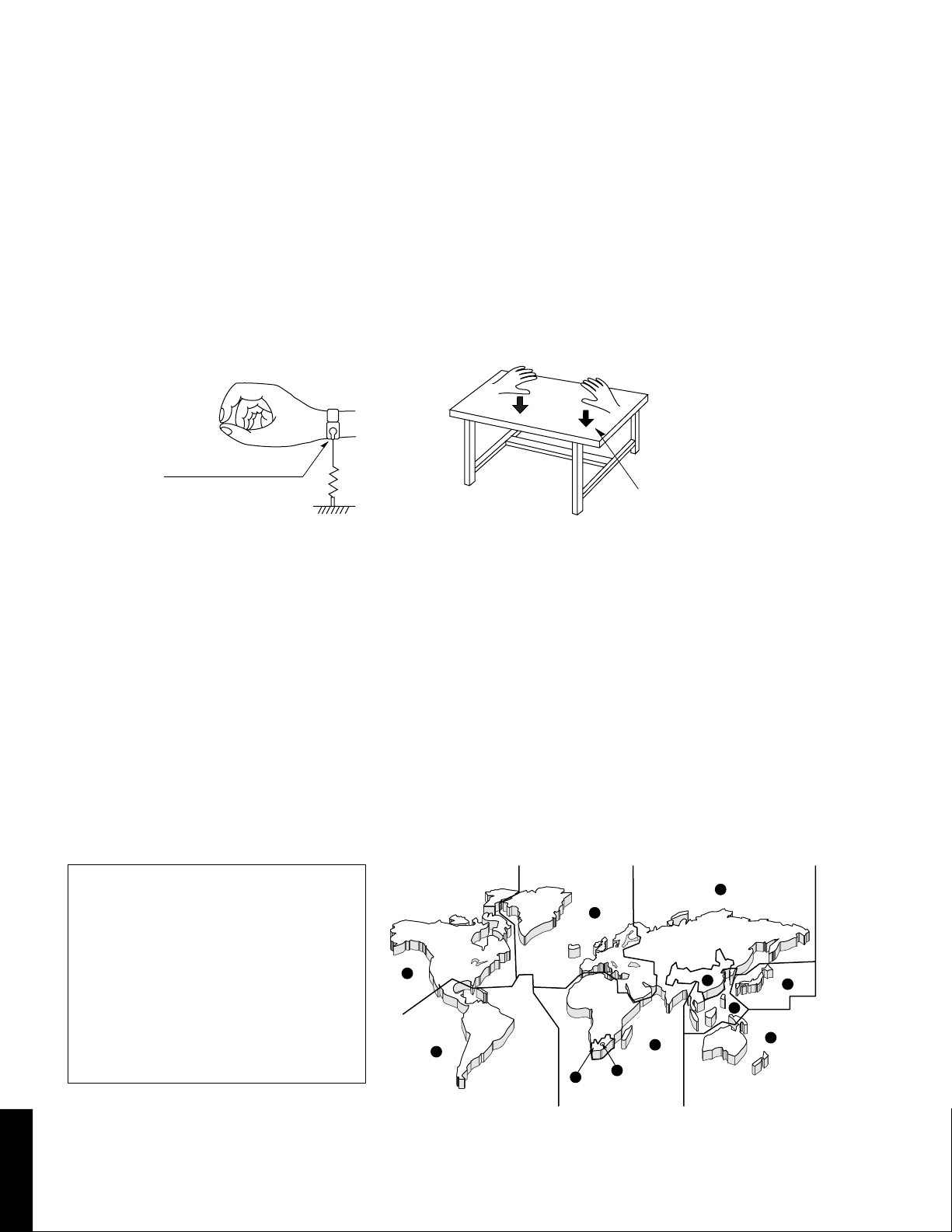
■ PREVENTION OF ELECTROSTATIC DISCHARGE
The laser diode in the DVD mechanism may be damaged due to static electricity from clothes or the human body. Use caution
to prevent electrostatic damage when servicing or handling the DVD-mechanism.
1. Grounding for electrostatic damage prevention
Some devices, such as the DVD player, use an optical pickup (laser diode) that will be damaged by static electricity in the
working environment. Only attempt service after ensuring that all grounding procedures have been completed.
1. Worktable grounding
Put a grounded conductive material (sheet) or iron sheet on the area where the optical pickup is placed.
2. Human body grounding
Use an anti-static wrist strap to discharge the static electricity from your body.
Anti-static wrist strap
1M-ohms
Conductive material
(sheet) or steel sheet
2. Handling Precautions for DVD mechanism
1. Handle the DVD mechanism gently, as it is an extremely high-precision assembly.
2. The flexible cable lines may break if an excessive force is applied to it. Use caution when handling the cable.
3. The semi-fixed resistor for laser power adjustment should not be adjusted. Do not turn the resistor.
■ LOCALE MANAGEMENT INFORMATION
Locale Management Information : This DVD player is designed and manufactured to respond to the Locale
Management Information that is recorded on a DVD disc. If the Locale number described on the DVD disc does not
correspond to the Locale number of this DVD player, this DVD player cannot play this disc.
This product incorporates copyright protection technology that is protected by
method claims of certain U.S. patents and
other intellectual property rights owned by
Macrovision Corporation and other rights
owners. Use of this copyright protection
technology must be authorized by
Macrovision Corporation, and is intended
for home and other limited viewing uses
only unless otherwise authorized by
Macrovision Corporation. Reverse engineering or disassembly is prohibited.
2
1
4
2
5
5
5
6
3
2
4
4
DV-S6160
DVD-S661/
Page 5
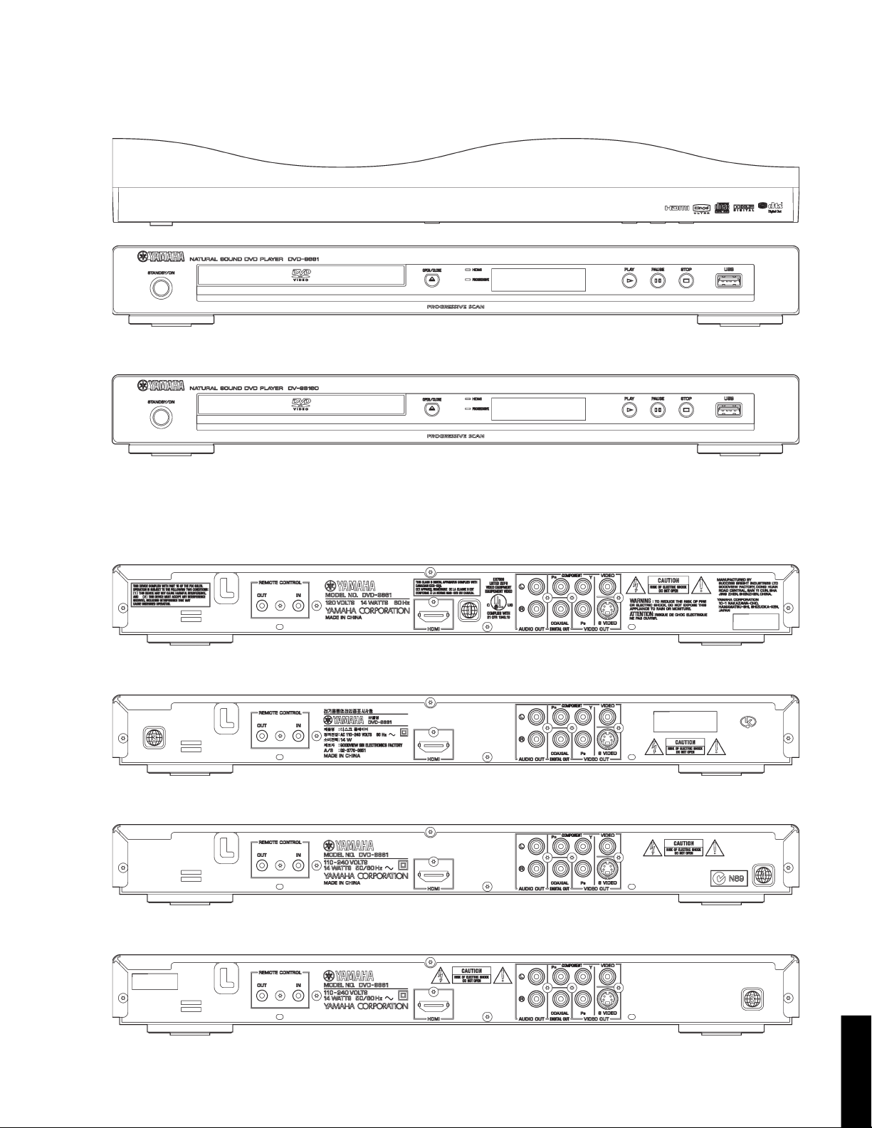
■ FRONT PANELS
DVD-S661 (U, K, A, L, P models)
DV-S6160 (U model)
DVD-S661/DV-S6160
■ REAR PANELS
DVD-S661 (U model)
DVD-S661 (K model)
DVD-S661 (A model)
DVD-S661 (L model)
5
DVD-S661/
DV-S6160
Page 6
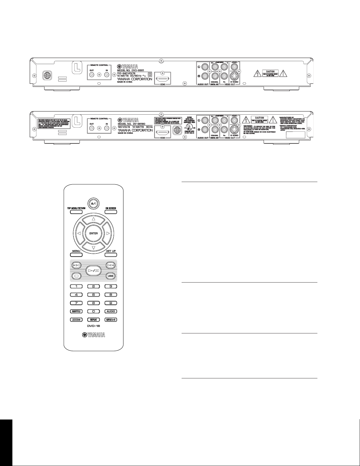
DVD-S661/DV-S6160
DVD-S661 (P model)
DV-S6160 (U model)
■ REMOTE CONTROL PANEL
■ SPECIFICATIONS
PLAYBACK SYSTEM
DVD Video, VR (Video Recording) format (DVD-RW)
DVD-R, DVD-RW, DVD-R DL
DVD+R, DVD+RW, DVD+R DL
Video CD, SVCD
CD
PICTURE CD
CD-R, CD-RW
MP3 (ISO 9660) fs 32, 44.1, 48 kHz / 96, 128, 256,
320 kbps (Constant bit rate)
WMA fs 44.1 kHz, 62 to 192 kbps /
fs 48 kHz, 128 to 192 kbps (Constant
bit rate)
DivX
JPEG 3072 x 2048 dpi or less
VIDEO PERFORMANCE
Video (CVBS) output 1 Vpp into 75 ohms
S-Video output Y: 1 Vpp into 75 ohms
C: 0.3 Vpp into 75 ohms
Component video output Y: 1 Vpp into 75 ohms
PB/PR: 0.7 Vpp into 75 ohms
HDMI upscaling 720 p, 1080 i
AUDIO FORMAT
Digital
Dolby Digital, DTS, MPEG
Compressed digital
PCM fs 44.1, 48, 96 kHz / 16, 20, 24 bits
Analog sound Stereo
6
DV-S6160
DVD-S661/
AUDIO PERFORMANCE
DA converter 24 bits
Signal to noise (1 kHz) 105 dB
Dynamic range (1 kHz) 97 dB
DVD fs 96 kHz 2 Hz to 44 kHz
fs 48 kHz 2 Hz to 22 kHz
SVCD fs 48 kHz 2 Hz to 22 kHz
fs 44.1 kHz 2 Hz to 20 kHz
CD/VCD fs 44.1 kHz 2 Hz to 20 kHz
Distortion and noise 0.0035 %
(1 kHz)
Page 7
DVD-S661/DV-S6160
310
(12-3/16")
6
(1/4")
318
(12-1/2")
2
(1/16")
435 (17-1/8")
6
(1/4")
45
(1-3/4")
51
(2")
MULTIMEDIA (USB) APPLICATIONS
Connections USB mass storage class device
Playback formats
(USB device)
MP3 fs 32, 44.1, 48 kHz / 96, 128, 256,
320 kbps (Constant bit rate)
WMA fs 44.1 kHz, 62 to 192 kbps /
fs 48 kHz, 128 to 192 kbps (Constant
bit rate)
DivX 3 Mbps or less
JPEG 3072 x 2048 dpi or less
Supported USB devices FLASH memory
(FAT16 or FAT32 format) Card reader (up to 6 slots)
Portable audio player
External hard disk drive (80 GB or less)
TV STANDARD (PAL/50 Hz) (NTSC/60 Hz)
Number of lines 625 525
Playback Multistandard (PAL/NTSC)
CONNECTIONS
Video output RCA/Phono x 1 (yellow)
S-video output Mini DIN, 4 pins x 1
Component video output
Y output RCA/Phono x 1 (green)
PB output RCA/Phono x 1 (blue)
PR output RCA/Phono x 1 (red)
Audio output (L+R) RCA/Phono x 1 pair (white/red)
Digital output
Coaxial RCA/Phono x 1
IEC60958 for CDDA, LPCM / IEC61937
for MPEG 1/2, Dolby Digital and DTS
HDMI (HDMI 1.0) Type A x 1
USB Type A x 1
Remote control
Input 3.5 mm mini jack x 1
Output 3.5 mm mini jack x 1
Manufactured under license from Dolby Laboratories. “Dolby”, “Pro Logic” and the double-D
symbol are trademarks of Dolby Laboratories.
“DTS” and “DTS Digital Out” are registered
trademarks of DTS, Inc.
DivX, DivX Ultra Certified, and associated
logos are trademarks of DivX, Inc. and are
used under license.
HDMI, the HDMI logo and High Definition
Multimedia Interface are trademarks or registered trademarks of HDMI Licensing LLC.
This product incorporates copyright protection technology
that is protected by method claims of certain U.S. patents
and other intellectual property rights owned by Macrovision
Corporation and other rights owners. Use of this copyright
protection technology must be authorized by Macrovision
Corporation, and is intended for home and other limited
viewing uses only unless otherwise authorized by Macrovision
Corporation. Reverse engineering or disassembly is prohibited.
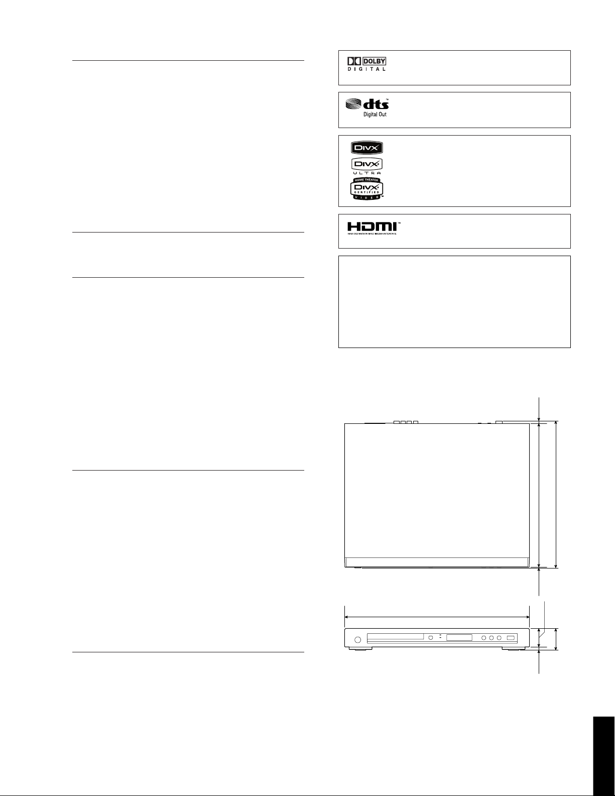
• DIMENSIONS
GENERAL
Dimensions (W x H x D) 435 x 51 x 318 mm
(17-1/8" x 2" x 12-1/2")
Weight Approx. 2.6 Kg (5 lbs. 12 oz)
Finish
DVD-S661 Black color (U, A, P models)
Titanium color (U, K, L models)
Silver color (U model)
DV-S6160 Black color (U model)
Silver color (U model)
Power supply AC 120 V, 60 Hz (U model)
AC 110-240 V, 60 Hz (K model)
AC 110-240 V, 50/60 Hz
(A, L, P models)
Power consumption Approx. 14 W
Standby power consumption Less than 1 W
ACCESSORIES
* Specifications are subject to change without prior notice.
Remote control x 1
Battery (AAA, R03, UM-4) x 2
Audio / video cable (1.5 m) x 1
U ........ U.S.A. model
K ........ Korean model
A ........ Australian model
L ......... Singapore model
P ......... South America model
Unit: mm (inch)
7
DVD-S661/
DV-S6160
Page 8
DVD-S661/DV-S6160
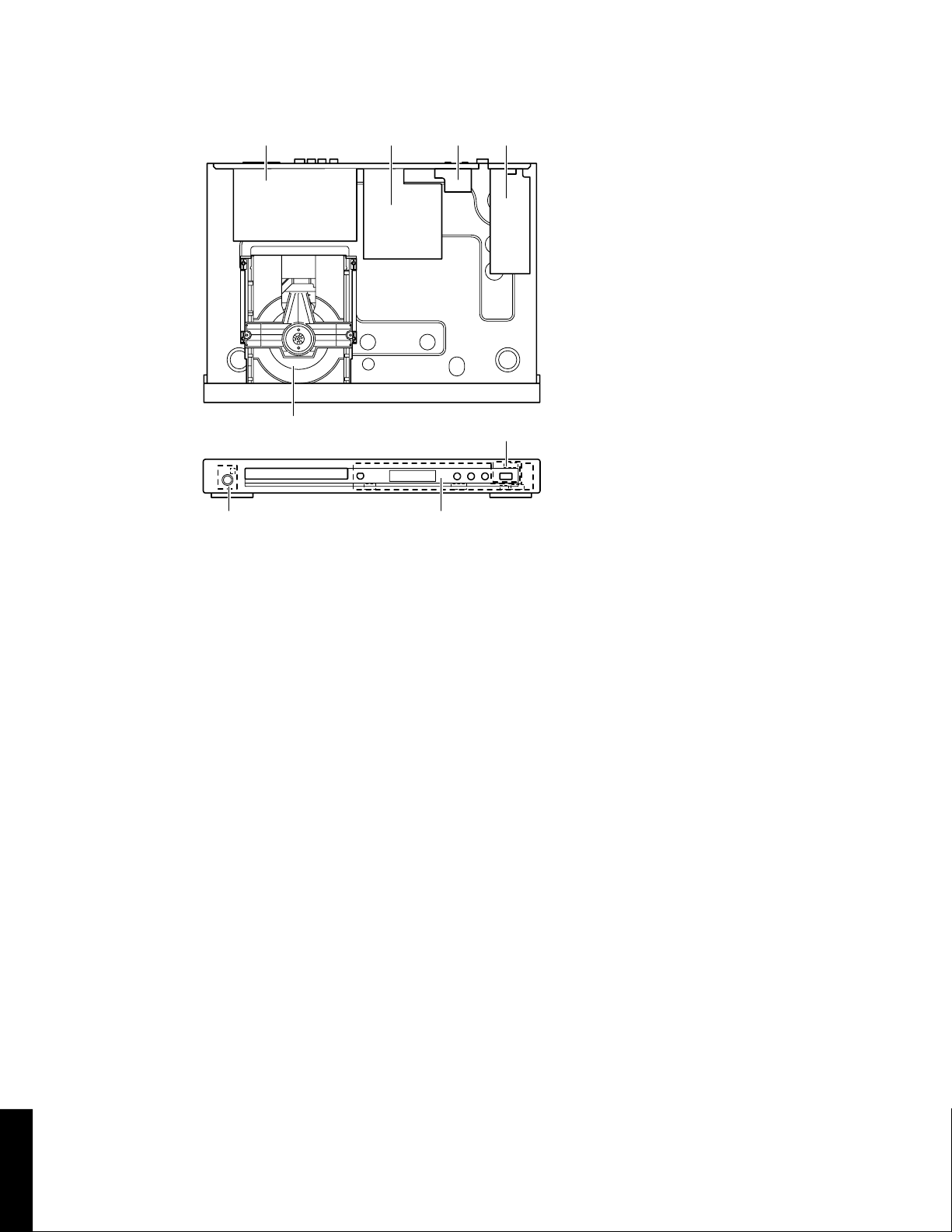
■ INTERNAL VIEW
1 432
1
AV P.C.B.
2
MONO P.C.B.
3
FRONT (4) P.C.B.
4
Power Supply Unit
5
DVD Mechanism
5
6 7
8
6
FRONT (2) P.C.B.
7
FRONT (1) P.C.B.
8
FRONT (3) P.C.B.
8
DV-S6160
DVD-S661/
Page 9
DVD-S661/DV-S6160
■ REPAIR NOTES
None of the components of the following unit can be supplied separately.
Each unit must be replaced as a whole in case of a failure.
• DVD Mechanism
• MONO P.C.B.
• FRONT P.C.B.
• AV P.C.B.
• Power Supply Unit
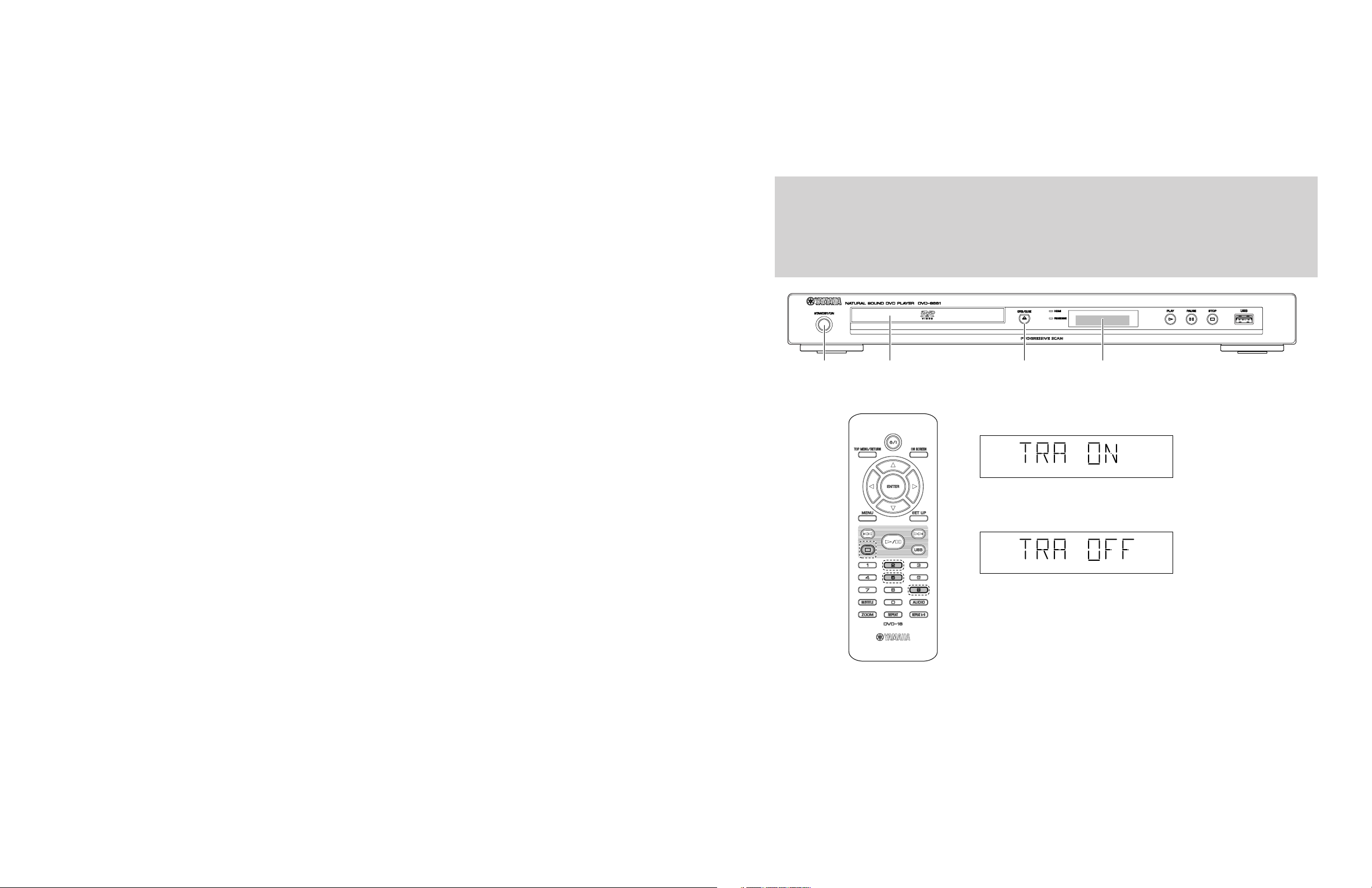
■ TRADE MODE
This unit provides TRADE mode which prevents the tray from opening even when the “OPEN/CLOSE” key is pressed.
• Activating TRADE mode
The power to the main unit should be turned on before activating the TRADE mode.
1. Press the “OPEN/CLOSE” key to open the tray. (Fig. 1)
2. Press the “2”, “5” and “9” keys on the remote control in that order. (Fig. 2)
3. “TRA ON” is displayed and TRADE mode is activated. About 2 seconds later, the tray is closed automatically. (Fig. 3)
Notes) • After activating TRADE mode, it is not possible to operate keys of the main unit as usual except the
following key.
“STANDBY/ON” key (Turn on the power only)
But operation with the remote control is available as usual.
• After TRADE mode is activated, initial settings for repeat reproduction of this unit are as follows.
DVD : RPT TT (repeat title)
VCD/SVCD/CD : RPT ALL (repeat all)
"STANDBY/ON" key Tray FL Display"OPEN/CLOSE" key
Fig. 1
TRADE mode display
Enter
Fig. 3
Cancel
Fig. 4
Fig. 2
• Canceling TRADE mode
The power to the main unit should be turned on before canceling TRADE mode.
1. Press and hold the “STOP” key on the remote control. (Fig. 2)
The tray opens after about 2 second.
2. Press the “2”, “5” and “9” keys on the remote control in that order. (Fig. 2)
3. “TRA OFF” is displayed and TRADE mode is cancelled. About 2 seconds later, the tray is closed automatically. (Fig. 4)
9
Page 10

DVD-S661/DV-S6160
■ DISASSEMBLY PROCEDURES
See REPLACEMENT PARTS LIST for item numbers.
Top Cover [240]
Remove 5 screws [250] (2 on sides and 3 on
rear side).
Lift cover from rear side to remove.
Mounting
Dismounting
When disassembling, use T10 TORX screwdriver as shown below.
T10
2.7 mm
Front Panel [101]
Remove 4 cables connections. [1105] [1205] [CN3] [1301]
Open tray. (Fig. 2)
Unlock tray lid and close tray.
Remove 2 screws [251] (Front panel to frame).
Unlock front panel by releasing successively 4 snaps (2 on sides
and 2 on bottom side).
FRONT (3) P.C.B. [1001 (3)]
Remove 2 screws [260] (P.C.B. to front
panel).
Dismount P.C.B..
FRONT (1) P.C.B. [1001 (1)]
Remove 4 screws [260] (P.C.B. to front
panel).
Dismount P.C.B..
Cable connections
Lock
(MONO P.C.B.)
1101
Flexible flat cable
FRONT (2) P.C.B. [1001 (2)]
Remove 2 screws [260] (P.C.B. to front
panel).
Dismount P.C.B..
Remove cable connection [1200
(FRONT P.C.B.)].
1201
(AV P.C.B.)
1200
(AV P.C.B.)
1201
(MONO P.C.B.)
1100
MONO P.C.B.AV P.C.B.
DVD Mechanism [1300-1]
Solder the lands of the optical pick up. (Fig. 3)
Remove 3 cable connections [1101] [1102] [1103].
Open tray. (Fig. 2)
Unlock tray cover ass'y and close tray.
Remove 4 screws (DVD mechanism to frame).
Lift DVD mechanism up slightly and move it backward
to remove.
Remove 3 cable connections [1100] [1200 (AV P.C.B.)]
[1201 (AV P.C.B.)].
Remove 3 screws [260] (P.C.B. to rear panel).
Release 2 locking spacers (P.C.B. to frame).
Dismount P.C.B..
FRONT (4) P.C.B.
1301
Power supply unit
CN101
1207
1205
CN3
MONO P.C.B. [1003]
Solder the lands of the optical pick up. (Fig. 3)
Remove 7 cable connections
[1201 (MONO P.C.B.)] [1205] [1207].
Remove 3 screws [256] (P.C.B. to frame).
Remove screw [260] (P.C.B. to rear panel).
Dismount P.C.B..
AV P.C.B. [1002]
[1101] [1102] [1103] [1105]
FRONT (4) P.C.B. [1001 (4)]
Remove cable connection [1301].
Remove 2 screws [260] (P.C.B. to rear panel).
Dismount P.C.B..
How to manually eject the tray
a. Move the slider in the direction indicated with a flatblade
screwdriver until the tray is ejected.
b. Gently pull the tray out.
Tr ay
Power Supply Unit [1005]
Remove 3 cable connections [CN101] [CN1] [CN3].
Remove 2 screws [256] (P.C.B. to frame).
Release 2 locking spacers (P.C.B. to frame).
Dismount power supply unit.
Preventive measure for laser diode from
electrostatic breakdown
When replacing the MONO P.C.B. or DVD
mechanism, solder between lands of the optical
pick up P.C.B. to protect the laser diode against
electrostatic breakdown.
Notes
• Use an anti-static soldering iron to shortcircuit and unshort-circuit laser diode.
• After you have finished repairing, remove the
solder from the short-circuit location.
10
Unlock
Flexible flat cable
DVD mechanism Front panel1103110511021101
FRONT (1) P.C.B.
View A
A
FRONT (2) P.C.B.FRONT (3) P.C.B.
1200
(FRONT P.C.B.)
CN1
Bottom side
Flatblade screwdriver
Optical pick up
Slider
Solder
Flatblade screwdriver
Fig. 3Fig. 1 Fig. 2
Page 11

■ TEST MODE
• Starting Test Mode
a. Connect the power cable to the AC power outlet.
b. Press the “STANDBY/ON” key while simultaneously pressing “PAUSE” and “STOP” keys of the main unit.
At this time, keep pressing “PAUSE” and “STOP” keys for 8 seconds or longer.
c. The “FV xx” (firmware version) is displayed.
DVD-S661/DV-S6160
• Display Test
The display condition varies as shown below according to the “PLAY” key of the main unit.
(OFF)
(OFF)
(ON)
(ON)
(OFF)
(OFF)
Initial display
All segments on
Lighting of segments in lattice
• Panel Key Test
The display changes as shown below as the specified key is pressed.
Press “OPEN/CLOSE” key of the main unit.
Press “STANDBY/ON” key of the main unit.
Press “OPEN/CLOSE” key of the main unit.
Press “PLAY” key of the main unit.
Press “PAUSE” key of the main unit.
Press “STOP” key of the main unit.
Press “PLAY/PAUSE” key of the remote controller.
• Canceling Test Mode
Disconnect the power cable from the AC power outlet.
Initial display
11
Page 12

ABCDEFGH I J
DVD-S661/DV-S6160
1
2
3
■ BLOCK DIAGRAM
DIGITAL OUT
COAXIAL
VIDEO
VIDEO OUT
S-VIDEO
COMPONENT
Y / P
B / PR
SC/SY
179,181
187
189,191
182,183,185
MONO
• See page 20-22 → SCHEMATIC DIAGRAM
7301
TZA1039HL
38,39
216
7108
+5D
+5STBY
206
211
215
98
99
209
210
197
HDMI
AV
• See page 23, 24 → SCHEMATIC DIAGRAM
+5D+5VL
L7805
IN
OUT
GND
7207
7216-7219
CLK
DIV.
MCLK
SCF
SCF
7208
DZFL
DZFR
AOUTL+
AOUTL-
AOUTR+
AOUTR-
16
15
12
11
10
9
AUDIO OUT
L / R
AK4385ET
CSN
6
CCLK
7
8
4
2
3
CDTI
LRCK
BICK
SDTI
uP
INTERFACE
DATA AUDIO
INTERFACE
PDN
5
DE-AMPHASIS
CONTROL
8 x
INTERPOLATOR
8 x
INTERPOLATOR
14 1
VDD
MOD
MOD
VSS
13
7112
+1V8
7113
4
DV3 3
47,48
109
3
D+/D-
7106
1
2
98
99
100
1521
+5V_STBY
7300
USB
14
IN
REMOTE
AV
• See page 23, 24 → SCHEMATIC DIAGRAM
INT_IR
OUT
GND
EXT_IR
7102
VS
32
SFH615
1100
OUT
CONTROL
7103-7105
5
Power Supply Unit
7100
8
5,6
9
DVD Mechanism
+12V
6
-12V
15-37
14,38
27
1105-1108
10-12
KEY1-3
6121,6122
41,42
+5V
AC IN
FRONT
7
12
• See page 25, 26 → SCHEMATIC DIAGRAM
Page 13

ABCDEFGH I J
1
■ WIRING DIAGRAM
DVD-S661/DV-S6160
30FE-BT-VK-N
1100
MCLK
1
2
GND
BCLK
3
4
GND
5
AC IN
2
CN101
2P JST-VA/VH
1002
AV P.C.B.
3
1005
Power Supply Unit
+5Vstby
GND
+5Vstby
GND
+12VA
+5Vstby
-12VA
STBY_PSU
JST EH
CN1
1
2
3
4
5
6
7
8
8P
JST EH
1200
1
+5Vstby
2
GND
3
+5Vstby
4
GND
5
+12VA
6
+5Vstby
7
-12VA
8
STBY_PSU
LRCLK
GND
PCM_DATA0
PCM_DATA1
PCM_DATA2
GND
SPDIF
GND
CVBS
GND
Y_G
GND
B_Cb_Pb
GND
R_Cr_Pr
VSCK
VSDA
MUTE_CTRL1
GND
GND
GND
6
7
8
9
10
11
12
13
14
15
16
17
18
19
20
S0
21
S1
22
23
24
25
NC
26
Y
27
28
C
29
30
8100
FFC 30P/060/30P AD
4
30FE-BT-VK-N
1201
1
2
3
4
5
6
7
8
9
10
11
12
13
14
15
16
17
18
19
20
21
22
23
24
25
26
27
28
29
30
MCLK
GND
BCLK
GND
LRCLK
GND
PCM_DATA0
PCM_DATA1
PCM_DATA2
GND
SPDIF
GND
CVBS
GND
Y_G
GND
B_Cb_Pb
GND
R_Cr_Pr
S0
S1
VSCK
VSDA
MUTE_CTRL1
NC
Y
GND
C
GND
1003
MONO P.C.B.
DVM9.1
PH 1104
SERVICE
1
GND
TXD
432
NC
RXD
STBY_PSU
PCB_LRCLK
STBY_FRONT
+5VL
GND
+5STBY
+5Vstby
VSDA
VSCK
VSTB
GND
+5VL
GND
+5V
IR
P+
P-43
B4B-EH-A
1105
1
2
EH 1207
1
2
3GND
4
5
PH 1206
1
2
3
4
5
6
7
8
9
WH04D-1
1522
GND
4P
1
P+
2
P-43
+5V
1001
FRONT (3) P.C.B.
+5Vstby
GND
+12VA
-24V
CN3
JST EH
GND
12345
1201
B5B-EH-A
GND
+5VL
GND
12345
+5Vstby
STBY_PSU
GND-LD
1101
SFV24R-1STSFV24R-1ST
NC
LD-DVD
HFM
MD
LD-CD
VR-DVD
62354321
NC
VR-CD
SP-
SP+
L_SW
GND
SLED-
T-
RF
CD/DVD
VcFVCC
GND-PDBA
E
C
F-T+F+
D
181716
151413121110987
24
222120
19
PH 1102
SLED+
65432
1
LOAD+
PH 1103
TROUT
LOAD-
GND
TRIN
54321
5
12345
EH 1101
GND
5P
GND
+12VA
-24V
+5Vstby
STBY_FRONT
GND
EH 1104 EH 1200
1
2
2P
1001
12STBY_FRONT
GND
NC
LD-DVD
GND-LD
HFM
MD
62354321
LD-CD
VR-DVD
987
NC
VR-CD
8009
10
E
Vc
VCC
3139 241 00391
GND-PD
FFC 24P/280/24P AD
0.5mmP
1514131211
F
B
A
D
C
T-
RF
CD/DVD
24
22212019181716
F-
T+
F+
6P
PH
1
SP+
SP-
GND
L_SW
65432
SLED-
SLED+
PH
5P
LOAD-
LOAD+
GND
TROUT
54321
TRIN
FRONT (2) P.C.B.
6
1001
FRONT (1) P.C.B.
+5Vstby
123
PH 1102
VSTB
VSDA
VSCKIR+5VL
GND
4
567
PCB_LRCLK
STBY_FRONT
9
8
+5V_STBY
GND
EXT_IR 3
WH03D-1
1103
1
2
B3B-EH-A
1301
+5V_STBY
3P
1
GND
2
EXT_IR3
1004
DVD Mechanism
WXD8829
1001
FRONT (4) P.C.B.
9P
7
5P
13
Page 14

DVD-S661/DV-S6160
■ PRINTED CIRCUIT BOARDS
FOR INFORMATION ONLY (COMPONENT PARTS NOT AVAILABLE)
MONO
(Top view)
HDMI
The first digit of a component indicates the component type.
1xxx : Connector 3xxx : Resistor 5xxx : Coil 7xxx : IC, Transistor, FET
2xxx : Capacitor 4xxx : SMD jumper 6xxx : Diode 9xxx : Wire jumper
AV
(1100)
AV
(1201)
14
DVD Mechanism Unit
FRONT (3)
(1522)
FRONT (1)
(1102)
DVD Mechanism Unit
Page 15

DVD-S661/DV-S6160
The first digit of a component indicates the component type.
1xxx : Connector 3xxx : Resistor 5xxx : Coil 7xxx : IC, Transistor, FET
2xxx : Capacitor 4xxx : SMD jumper 6xxx : Diode 9xxx : Wire jumper
MONO
(Bottom view)
15
Page 16

DVD-S661/DV-S6160
AV (Top view)
VIDEO/
S-VIDEO
COMPONENT
B, PR
Y, P
DIGITAL OUT
COAXIAL
The first digit of a component indicates the component type.
1xxx : Connector 3xxx : Resistor 5xxx : Coil 7xxx : IC, Transistor, FET
2xxx : Capacitor 4xxx : SMD jumper 6xxx : Diode 9xxx : Wire jumper
AUDIO OUT
L/R
Power Supply Unit (CN1)
(1201)
MONO
(1207)
MONO
16
Page 17

AV (Bottom view)
DVD-S661/DV-S6160
The first digit of a component indicates the component type.
1xxx : Connector 3xxx : Resistor 5xxx : Coil 7xxx : IC, Transistor, FET
2xxx : Capacitor 4xxx : SMD jumper 6xxx : Diode 9xxx : Wire jumper
17
Page 18

DVD-S661/DV-S6160
The first digit of a component indicates the component type.
1xxx : Connector 3xxx : Resistor 5xxx : Coil 7xxx : IC, Transistor, FET
2xxx : Capacitor 4xxx : SMD jumper 6xxx : Diode 9xxx : Wire jumper
FRONT (1)
(Top view)
OPEN/CLOSE
PROGRESSIVE
FRONT (2)
(1200)
HDMI
LED
LED
PLAY PAUSE STOP
MONO
(1206)
FRONT (4)
(1301)
Power Supply Unit
(CN3)
FRONT (1)
(Bottom view)
18
Page 19

DVD-S661/DV-S6160
The first digit of a component indicates the component type.
1xxx : Connector 3xxx : Resistor 5xxx : Coil 7xxx : IC, Transistor, FET
2xxx : Capacitor 4xxx : SMD jumper 6xxx : Diode 9xxx : Wire jumper
FRONT (2)
(Top view)
FRONT (1)
(1104)
STANDBY/ON
FRONT (3)
(Top view)
USB
MONO
(1105)
FRONT (4)
FRONT (1)
OUT IN
REMOTE CONTROL
(Top view)
(1103)
FRONT (2)
(Bottom view)
FRONT (3)
(Bottom view)
FRONT (4)
(Bottom view)
19
Page 20

DVD-S661/DV-S6160
■ SCHEMATIC DIAGRAMS
FOR INFORMATION ONLY (NO COMPONENT PARTS NOT AVAILABLE)
MONO 1/3
A
B
C
To DVD Mechanism Unit
D
E
F
G
LIMIT
H
1103
B5B-PH-K
1
2
3
4
5
I
1 789
+RF_V5
1101
SFV24R-1ST
1
2
3
4
5
6
7
8
9
10
11
12
13
14
15
16
rf
17
18
19
20
21
22
23
24
2526
1102
B6B-PH-K
T125
6
T126
5
T127
4
T128
3
T129
2
T130
1
5158
22p
100n
2142
2185
T131
T132
T133
T134
T135
22p
22p
22p
22p
22p
2136
2139
2163
2162
2160
123
2
5140
BLM18P
+1V8
2161 100n
2158 220u
+5VL
+RF_V5
5145
BLM18P
100n
2186
100n
2112
220u
2111
5152
BLM18P
T101
T102
3132
390R
T103
T104
T105
T106
T107
T109
E
T110
T111
T113
T114
T115
T116
T117
T118
T119
T120
T121
T122
T123
4127
4130
3146150K
3145
10K
OP+
DV33
4132
60R
4133
60R
60R
4138
413960R
60R
4147
BC847B
7106
V20
F
2127
100n
B_
A_
D_
C_
T-
2002
T+
F+
22p
F-
SL+
SL-
SP+
SP-
1R03143
3147150K
OP-
LOAD+
LOAD-
TROUT
TRIN
DV33
4K7 3158
34
74HC1G04GW
+V18
33p
2164
FOSO
TRSO
FMSO
DMSO
330p
2105
10K3140
5156
2133
100n
+5V_STBY
DMSO
3149
10K
3
10K
3150
TROUT
TRIN
STBY
3131
4R7
2
7105
1
BC807-25
3134
100R
3
1
7109
BC817-25W
2
IOA
+5VL
50R
5159
BLM31
50R
FOSO
3148
10K
FMSO
TRSO
TRCLOSE
TROPEN
TRB1
D
TRB2
V1P4
10K
3155
5151
10u
5153
10u
3133
100R
3136
100K
+5M
2144
100n
D
31574K7
BC847B
7107
+L_V33
3137
330p
2106
2115
47u 16V
+RF_V5
100K
3139
10K
USB_LIMITER_OE
+5M
USB_OVERCURRENT
100n2199
AM5888S
100n
2148
D
2107
3171
4K7
7111
1
4
23
26
21
6
7
2
25
27
28
20
24
DV33
2101
100n
7115
5
2
1
NC
3
1
3116 100K
16M5141
15n
100n
2108
3
1
BC807-25
V20
V2P8
47u2119
100n2120
2121 47u
7110
TPS2051D
4
EN
2
1
IN
2
2138
D
47u 16V
MOTOR DRIVER
VINFC
VINSL+
VINLD
VINTK
VTCL
FWD
REV
1
TRB
2
BIAS
MUTE
NC
PGND
GND
22
29
D
D
74HC1G04GW
4
3123
27K
3124
27K
3125
15K
3126
10K
2
7104
100n2122
2123 47u
GND
1
+5M
8
VCC
VOFC
VOSL
VOLD
VOTK
VOTR
REGO
30
D
to FRONT (3)_1522
4567
56
7116
2
22p
2165
V1P4
3130
4R7
V1P4
2124 100n
DISABLE_USB
1
23OUT
OC_
19
74HC1G04GW
5
1
NC
3
1
FOO
TRO
FMO
DMO
+L_V33
16V
2114
47u
6
7
8
5
USB_OVERCURRENT
14
+
13
-
11
+
12
17
+
18
-
15
+
16
-
10
+
9
-
5
1
3
2
Page 26
4
3166
5148
BLM18P
ADIN
OP-
OP+
V1P4
1
2
3
4
B4B-EH-A
2
33R
DV33
1105
PSS8550
7118
3172
470R
7117
5
1
NC
1
DV33
DV33
3169 15K
3170 15K
F+
F-
SP+
SP-
SL+
SL-
T-
T+
LOAD+
LOAD-
REGO1
REGO2
3
DV33
5154
2117
2118 100n
2125 2n2
470R
A1
The first digit of a component indicates the component type.
1xxx : Connector 3xxx : Resistor 5xxx : Coil 7xxx : IC, Transistor, FET
2xxx : Capacitor 4xxx : SMD jumper 6xxx : Diode 9xxx : Wire jumper
10
DV33
470n2149
BLM18P
237
238
LPFOP
AD2
83
AD(3)
1n02170
236
LPFIP
LPFIN
AD384DVSS_285AD4
AD(4)
AD(5)
I2C_CLK1
I2C_DAT1
2150 10u
750K3118
235
LPFON
86
AD(6)
XTALI
234
PLLVDD3
AD588AD6
87
A21
D
VSCK
VSDA
VSTB
5144BLM18P
233
60R5139
100u 215310V
+V18
2171 100n
XO
230
231
232
JITFN
JITFO
PLLVSS
IDACEXLP
IOA21
ALE90AD791A1792IOA093DVSS_3
89
D
A(17)
AD(7)
+V18
100n
2151
D
100n
2155
3161 22R
3163 22R
2172
6.3V 4u7
229
DV33
3174
3175
3176
XTALI
A(0)
228
227
XTALO
94
6.3V 10u2189
225
226
RFVDD18
RFGND18
7108
MT1389
UWR#95URD#
96
223
224
SPDIF
MC_DATA
DVDD18_298UP1_299UP1_3
97
4144
MUTE_CTRL1
100R
100R
100R
222
DVSS_13
ASDATA4
DV33
1K0
3167
3168
4
5160
BLM18P
BLM18P
100n
680K3135
680K3138
2n22129
5155
BLM18P
3184
5157
BLM18P
D
D
DV33
TRB1
+1V8
REGO1
33R
2001
100u
C_
B_
A_
D_
2140
100n
+5V_STBY
27M
RFVDD
PSS8550
7113
D
+5D
1N4001
15K
3154
9K1
3160
1
2
3
4
5
6
7
8
9
10
11
12
13
14
15
16
17
18
19
20
21
22
23
24
25
26
27
28
29
30
31
32
33
34
35
36
37
38
39
40
41
42
43
44
45
46
47
48
49
50
51
52
53
54
55
56
57
58
59
60
61
62
63
64
V1P4
2192100n
AGND
DVDA
DVDB
DVDC
DVDD
DVDRFIP
DVDRFIN
MA
MB
MC
MD
SA
SB
SC
SD
CDFON
CDFOP
TNI
TPI
MDI1
MDI2
LDO2
LDO1
SVDD3
CSO
RFLVL
SGND
V2REFO
V20
VREFO
FEO
TEO
TEZISLV
OP_OUT
OP_INN
OP_INP
DMO
FMO
TROPENPWM
PWMOUT1
TRO
FOO
USB_VSS
USBP
USBM
USB_VDD3
FG
TDI
TMS
TCK
TDO
DVDD18_1
IOA2
IOA3
IOA4
IOA5
IOA6
IOA7
HIGHA0
IOA18
IOA19
DVSS_1
APLLCAP
APLLVSS
2145
100n
D
DV33
15K
3120
255
256
IREF
AVDD3
IOWR#
APLLVDD3
66
65
DV33
PWR
DV33
XTALI
RFVDD
2194
2193
2n2
100n
1u02196
2197 1u0
1u0
2102
2103 1u0
1u02104
T143
4122
4123
4124
4125
E
F
4126
T141
T142
T112
V2P8
T139
V20
T140
V1P4
T136
T138
100n2126
DMO
FMO
TROPEN
T137
TRO
FOO
2131
6n8
2132
100n
1106
100R
23
3182
100R
14
D
TRB2
REGO2
TROUT
TRCLOSE
2141
100n
4136
6105
1N4001
STBY
ADIN
TRIN
3183
A(2)
A(3)
A(4)
A(5)
A(6)
A(7)
A(8)
A(18)
A(19)
6104
ACM
+V18
PSS8550
7112
5K6
3153
10K
3159
D
2154 22p
3117
100n2178
2179 100n
253
254
OSN
RFGC
A16
HIGHA7
67
68
A(15)
A(16)
100K
252
OSP
HIGHA6
69
A(14)
251
70
2187 220u
2152
100n
2166
1n0
33n2180
100n
2181
250
248
249
CEQP
CEQN
RFGND
CRTPLP
DVDD3_1
HIGHA571HIGHA472HIGHA3
73
A(13)
A(12)
A(11)
A(10)
100n2188
RFVDD
247
HRFZC
HIGHA2
74
A(9)
246
RFRPAC
HIGHA1
75
A(20)
10V
RFVDD
100n2176
244
245
RFVDD3
RFRPDC
IOA2077IOCS#78IOA1
76
PCE
A(1)
100u2167
47n
2182
242
243
S_VREFN
79
PRD
DV33
100n2168
47n2183
240
241
ADCVSS
S_VREFP
DVDD3_2
IOOE#
80
D
AD(0)
AD(1)
6R83112
5142
239
S_VCM
AD081AD1
82
ADCVDD3
AD(2)
89
310233R
310133R
DV33
+V18
60R5143
SPDIF_OUT
AUX_DATA_IN
100n
10V 100u 2173
2175
316533R
312133R
2174 10u6.3V
33R 3122
218
219
214
215
216
217
220
221
ACLK
DVSS_12
ASDATA3
ASDATA0
ASDATA1
ASDATA2
DVDD18_6
UP1_7
UP3_0
UP3_1
UP3_4
UP1_4
UP1_5
UP1_6
102
103
104
105
106
107
100
101
3151 4K7
UP3_1
UP3_0
D
DV33
T155
T158
T156
T157
123
1104
B4B-PH-K
10 11
11 12
CENTRE_CH
USB_OVERCURRENT
SurrL
Lo
Ro
SurrR
SEL_0
SubW
MUTE_CTRL1
DV33
100n
100n
2156
PCM_DATA4
2157
PCM_MCLK
PCM_LRCLK
PCM_DATA3
PCM_BCLK
SPBCLK
207
208
209
212
213
210
211
ABCK
UP3_5
4
ALRCK
DVDD3_3
108
109
SPBCK
SPLRCK
DVDD3_10
PRST#
IR
ICE
110
111
4146
DQM0
RC6
SPDATA
INT0#
112
IOA
SPMCLK
DQM0
113
DQ7
114
DV33
HSYN
DQS0
DQ6
SPLRCLK
22R
3178
206
205
YUV7
RD7
115
116
DQ5
1
SPDATA
VSYN
DVSS_4
DQ4
PCM_DATA2
PCM_DATA1
SPMCLK
201
202
203
204
YUV5
YUV6
DVDD3_9
DACVSSA
RD6
RD5
DVSS_5
RD4
118
119
120
117
DQ1
DQ3
DQ2
100n2146
D
7114
NCP303LSN30
OUTP
GND
NC
3
200
121
4K7
4K7
3104
3105
310933R
100n2177
PCM_DATA0
3119 560R
197
198
199
193
194
195
196
YUV1
YUV2
YUV3
YUV4
DACVSSB
DACVSSC
DACVDDA
DACVDDB
DACVDDC
DVDD3_8
DVSS_11
DVDD18_5
DVDD3_7
DVSS_10
DVSS_9
DVDD3_6
RCLKB
RVREF
DVDD18_4
DVSS_8
DVSS_7
DVDD3_5
DVSS_6
RD3
DVDD18_3
RD2
RD1
RD0
RD15
DVDD3_4
RD14
122
123
124
125
126
127
128
DQ11
DQ13
DQ12
DQ0
DQ15
DQ14
DQ9
DQ10
2
INP
+5D
5
CD
2159
100n
4
DV33
12 13
DV33
YUV0
VREF
RD16
RD17
RD18
RD19
RD20
RD21
RD22
RD23
DQM2
DQM3
RD24
RD25
RD26
RD27
RD28
RD29
RD30
RD31
RA11
CKE
RCLK
RA10
RCS#
RAS#
CAS#
RWE#
DQM1
DQS1
RD8
RD9
RD10
RD11
RD12
RD13
I2C_DAT
I2C_CLK
+V_V33
FS
RA4
RA5
RA6
RA7
RA8
RA9
RA3
RA2
RA1
RA0
BA1
BA0
3152
RDS_DATA
2184
100n
192
191
190
189
188
187
186
185
184
183
182
181
180
179
178
177
176
175
174
173
172
171
170
169
168
167
166
165
164
163
162
161
160
159
158
157
156
155
154
153
152
151
150
149
148
147
146
145
144
143
142
141
140
139
138
137
136
135
134
133
132
131
130
129
10K
13 14
+V_V33
2169
100n
DV33
5147
BLM18P
#Y
#C
#CVBS
#Y_G
#B_Cb_Pb
#R_Cr_Pr
HDMI_RST
HDMI_C0
HDMI_C1
HDMI_C2
HDMI_C3
HDMI_C4
HDMI_C5
HDMI_C6
HDMI_C7
HDMI_VCK
HDMI_Y0
HDMI_Y1
HDMI_Y2
HDMI_Y3
HDMI_Y4
HDMI_Y5
HDMI_Y6
HDMI_Y7
MA4
MA5
MA6
MA7
MA8
MA9
MA11
DCKE
DCLK
MA3
MA2
MA1
MA0
MA10
BA1
BA0
CS
D
RAS
CAS
WE
DQM1
LIMIT
DQ8
2143 100n
22R 3162
UP3_1
22R
UP3_0
16V10u
2147
2003
100n
+V_V33
2191 100n
2190 10u
+V_V33
2195
100n
+V_V33
2109
100n
3127 47R
3129 47R
D
2113
100n
+V18
DV33
2116
100n
+V18
2128
100n
DV33
2130
D
100n
2134
100n
DV33
+V18
2137
100n
DV33
STBY_PSU
3164
STBY_FRONT
3177
7119
BC817-25W
22K
HDMI_VSYN
HDMI_HSYN
DISABLE_USB
14
1101 D1
1102 F1
1103 H1
1104 I10
1105 F5
1106 F6
2001 B6
2002 F2
2003 I13
2101 A4
2102 C6
2103 C6
A
2104 C6
2105 C3
2106 C4
2107 C4
2108 C4
2109 C14
2111 D2
2112 D2
2113 D13
2114 D5
2115 D3
2116 E13
2117 E5
B
2118 E5
2119 E4
2120 E4
2121 E4
2122 E4
2123 E4
2124 E5
2125 E5
2126 E6
2127 E2
2128 E13
2129 E5
C
2130 F13
2131 F6
2132 F6
2133 F3
2134 F13
2136 I1
2137 G13
2138 G4
2139 I1
2140 G6
2141 G6
D
2142 G1
2143 G13
2144 H3
2145 H7
2146 I11
2147 I13
2148 I4
2149 A9
2150 A9
2151 I9
2152 A8
2153 A9
E
2154 A8
2155 I9
2156 B10
2157 B11
2158 B2
2159 I12
2160 I1
2161 B2
2162 I1
2163 I1
2164 B4
2165 B5
F
2166 A8
2167 B8
2168 B8
2169 A13
2170 B9
2171 B9
2172 A9
2173 B10
2174 B10
2175 B10
2176 B8
G
2177 B12
2178 B8
2179 B8
2180 B8
2181 B8
2182 B8
2183 B8
2184 B12
2185 G1
2186 C2
2187 I8
2188 I8
H
2189 B10
2190 B13
2191 B13
2192 B7
2193 B6
2194 B6
2195 C13
2196 C6
2197 C6
2199 G3
3101 A10
3102 A10
3104 A12
I
3105 A12
3109 A12
3112 A9
3116 B4
3117 B8
3118 B9
3119 B12
3120 B7
3121 B10
3122 B10
3123 B4
3124 C4
3125 C4
3126 C4
3127 D14
3129 D14
3130 D5
3131 D3
3132 D2
3133 E3
3134 E3
3135 E5
3136 E2
3137 E3
3138 E5
3139 F3
3140 F3
3143 G2
3145 G2
3146 G2
3147 G2
3148 G3
3149 H3
3150 H3
3151 H10
3152 I12
3153 I6
3154 I7
3155 I3
3157 I3
3158 I3
3159 I6
3160 I7
3161 I9
3162 H13
3163 I9
3164 H13
3165 B10
3166 A5
3167 A6
3168 A6
3169 F5
3170 F5
3171 F4
3172 G5
3174 I9
3175 I9
3176 I9
3177 H13
3178 B11
3182 F7
3183 F7
3184 F5
4122 C7
4123 C7
4124 C7
4125 D7
4126 D7
4127 F2
4130 G2
4132 H2
4133 I2
4136 H7
4138 I2
4139 I2
4144 H10
4146 H11
4147 I2
5139 A9
5140 A2
5141 B4
5142 A9
5143 B10
5144 A9
5145 B2
5147 B13
5148 D5
5151 D3
5152 D2
5153 D3
5154 E5
5155 F6
5156 F3
5157 G6
5158 G1
5159 G3
5160 B6
6104 H7
6105 H6
7104 D4
7105 D3
7106 E2
7107 E3
7108 E10
7109 F3
7110 E4
7111 G4
7112 H6
7113 H7
7114 I11
7115 A4
7116 A5
7117 A5
7118 G5
7119 H14
T101 D2
T102 D2
T103 E2
T104 E2
T105 E2
T106 E2
T107 E2
T109 E2
T110 E2
T111 E2
T112 E7
T113 E2
T114 E2
T115 E2
T116 E2
T117 F2
T118 F2
T119 F2
T120 F2
T121 F2
T122 F2
T123 F2
T125 G1
T126 G1
T127 G1
T128 G1
T129 G1
T130 G1
T131 I1
T132 I1
T133 I1
T134 I1
T135 I1
T136 E7
T137 F7
T138 E7
T139 E7
T140 E7
T141 E7
T142 E7
T143 C7
T155 I10
T156 I10
T157 I10
T158 I10
20
Page 21

MONO 2/3
A
B
C
D
PCM_MCLK
E
F
G
H
I
3201
150R
3206
150R
3210
3212
PCM_BCLK
12
5201
5203
5205
5206
1u8
1u8
1u8
1u8
EN
DCLK
DCKE
MA0
MA1
MA2
MA3
MA4
MA5
MA6
MA7
MA8
MA9
MA10
MA11
BA0
BA1
RAS
CAS
2202
2206
2210
2212
PCM_DATA4
PCM_DATA0
PCM_LRCLK
DV33
100n 2268
5
3
74AHC1G125GW
DV33
CS
WE
R_Cr_Pr
47p
3202
B_Cb_Pb
47p
3207
Y_G
47p
3211
CVBS
47p
3213
4
7214
3237 150R
3239
3240 150R
3242 150R
3246 150R
3249 150R
3251 150R
3252
3253 47R
3254 150R
3270 150R
3261 150R
150R
150R
150R
150R
3214
33R
33R 3217
321833R
33R 3221
120R
3222
5211
BLM18P
16V
2241
47u
23
150R3233
0
24
150R3235
1
25
2
26
150R
3
29
4
30
150R3241
5
31
6
32
150R3244
7
33
8
34
150R3248
9
22
10
35
150R3250
11
20
0
21
150R
1
38
37
CKE
19
150R3256
CS
18
RAS
17
150R3259
CAS
16
WE
23
D
D
150R
D
150R
D
3267
100R
#R_Cr_Pr
47p
2201
#B_Cb_Pb
47p
2205
#Y_G
47p
2209
#CVBS
47p
2211
4216
2
1
1
345
#C
47p
2203
3203
150R
D
#Y
47p
2207
3208
150R
D
22R
3277
VSDA
VSCK
SEL_1
SEL_0
#PCM_MCLK
#PCM_BCLK
11427394349
A
1M-1
BA
CLK
2841546124652
3278
#PCM_DATA0
#PCM_LRCLK
#PCM_DATA1
#PCM_DATA2
VDD
1M X 16 X 4
0
IS42S16400A
VSS
22R
22p2214
#SPDIF_OUT
D
Φ
DRAM
7206
2215 22p
VDDQ
VSSQ
D
22p2216
5202
5204
DQM
1u8
1u8
2204
2208
2217 22p
2240
2242
2243
2245 100n
NC
0
1
2
3
4
5
6
7
8
9
10
11
12
13
14
15
H
L
47p
47p
MUTE_CTRL2
MUTE_CTRL1
1K03223
22p2218
100n
100n
100n
100n2246
100n2248
100n2249
36
40
2
4
5
7
8
10
11
13
42
44
45
47
48
50
51
53
39
15
3264 150R
6
C
3204
150R
Y
3209
150R
AUX_DATA_IN
1K03224
2219 22p
DQ7
DQ6
DQ5
DQ4
DQ3
DQ2
DQ1
DQ0
DQ8
DQ9
DQ10
DQ11
DQ12
DQ13
DQ14
DQ15
150R3263
S1
S0
3281
3225 1K0
22R
DQM1
DQM0
26FE-BT-VK-NA
D
1202
+3V3_FL
PWR
+3V3_FL
Page 23
F201
F202
26
F203
25
F204
24
F205
23
F206
22
F207
21
F208
20
F209
19
18
F210
17
16
F211
15
14
F212
13
12
F213
11
10
F214
9
F215
8
F216
7
6
F217
5
F218
4
F219
3
F221
2
F220
1
A(1)
A(2)
A(0:21)
A(3)
A(4)
A(5)
A(6)
A(7)
A(8)
A(9)
A(10)
A(11)
A(12)
A(13)
A(14)
A(15)
A(16)
A(17)
A(18)
A(19)
4210
A(20)
PRD
PCE
3257 10K
C1
to AV_1100
30FE-BT-VK-N
30
29
28
27
26
25
22p 2222
24
23
22p 2224
22
21
22p 2226
20
19
18
17
16
15
14
13
12
11
10
9
8
7
6
5
4
3
2
1
1201
D
7205
M29W160ET70
25
0
24
1
23
2
22
3
21
4
20
5
19
6
18
7
8
8
7
9
A
6
10
5
11
4
12
3
13
2
14
1
15
48
16
17
17
16
18
9
19
19
RB
RP
WE
OE
CE
BYTE
222122p
222322p
222522p
SPDIF_OUT
SPDIF_OUT
+3V3_FL
[FLASH]
2Mx8/1Mx16
0
2M-1 / 1M-1
27
PCM_LRCLK
D
HDMI_AUDIO_MUTE
37
VDD
VSS
46
456
D
STBY_FRONT
Page 24
0
1
2
3
4
5
6
7
D
8
9
10
11
12
13
14
15
A-1
NC
4203
4206
to AV_1201
74HC1G125GW
3219
1K0
4213
4214
5212
BLM18P
29
31
33
35
38
40
42
44
30
32
34
36
39
41
43
45
3255
13
22R
14
10
The first digit of a component indicates the component type.
1xxx : Connector 3xxx : Resistor 5xxx : Coil 7xxx : IC, Transistor, FET
2xxx : Capacitor 4xxx : SMD jumper 6xxx : Diode 9xxx : Wire jumper
7891011
Page 25
to FRONT (1)_1102
+5V_STBY
B9B-PH-K
B8B-PH-K-S
3205
+5V_STBY
STBY_PSU
1205
+5VL
VSDA
VSCK
VSTB
1K0
RC6
+5VL
4209
E1
2
1
100n2247
7201
AD(0)
AD(1)
AD(2)
AD(3)
AD(4)
AD(5)
AD(6)
AD(7)
DV33
EN
16V47u2244
A(0)
+3V3_FL
A21
5
3
AD(0:7)
4
BLM18P
2213
3220 22R
3227D22R
1206
F249
1
F222
1
F223
2
F224
3
F225
4
F226
5
F227
6
F228
7
F229
8
F246
F247
F248
D
5207
100n
1207
B5B-EH-A
DV33
D
#SPDIF_OUT
SPDIF_MT1392
10p
2
10p 2228
3
4
5
6
7
8
22p 2234
9
1
2
3
4
5
789
2227
222910p
223022p
223122p
223222p
E2
D
223522p
223622p
D
7212
M24C16-RDW6
EEPROM
1
0
2
ADR
1
3
2 SDA
D
10 11 12
12 13
DV33
3258
100n
84
Φ
(2Kx8)
D
7
WC
6
SCL
5
D
I2C_CLK
I2C_DAT
13
DVD-S661/DV-S6160
4203 B7
1201 D6
1202 D5
4206 B7
4209 B7
1204 A11
4210 H5
1205 A8
4213 D7
1206 A8
4214 F7
1207 B8
4216 D1
1208 A12
5201 A1
2201 A1
5202 A3
2202 A1
A
B
C
D
E
F
G
H
I
2203 A3
2204 A3
2205 B1
2206 B1
2207 B3
2208 B3
2209 B1
2210 B1
2211 C1
2212 C1
2213 D8
2214 E3
2215 E3
2216 E3
2217 E3
2218 E3
2219 E4
2221 C6
2222 C6
2223 C6
2224 C6
2225 C6
2226 C6
2227 A9
2228 A9
2229 B9
2230 B9
2231 B9
2232 B9
2234 B9
2235 C9
2236 C9
2240 F3
2241 F2
2242 F3
2243 F3
2244 F7
2245 F3
2246 F3
2247 F7
2248 F3
2249 F3
2266 B13
2267 B13
2268 D2
2269 A13
3201 A1
3202 A2
3203 A3
3204 A4
3205 B7
3206 B1
3207 B2
3208 B3
3209 B4
3210 B1
3211 B2
3212 C1
3213 C2
3214 C2
3217 D2
3218 D2
3219 D7
3220 D8
3221 D2
3222 E2
3223 E4
3224 E4
3225 E4
3227 E8
3233 G2
3235 G2
3237 G2
3239 G2
3240 G2
3241 G2
3242 G2
3244 G2
3246 G2
3248 G2
3249 G2
3250 G2
3251 H2
3252 H2
3253 H2
3254 H2
3255 H7
3256 H2
3257 H5
3258 E12
3259 H2
3261 H2
3263 H4
3264 H4
3267 D1
3270 H2
3277 B3
3278 B3
3281 D4
5203 B1
5204 B3
5205 B1
5206 C1
5207 D8
5211 F2
5212 F7
7201 D7
7205 F5
7206 G3
7212 E11
7214 E2
F201 B5
F202 B5
F203 C5
F204 C5
F205 C5
F206 C5
F207 C5
F208 C5
F209 C5
F210 C5
F211 C5
F212 C5
F213 D5
F214 D5
F215 D5
F216 D5
F217 D5
F218 D5
F219 D5
F220 D5
F221 D5
F222 A8
F223 A8
F224 B8
F225 B8
F226 B8
F227 B8
F228 B8
F229 B8
F230 A12
F231 A12
F232 A12
F233 B12
F234 B12
F235 B12
F236 B12
F237 B12
F238 C12
F239 B12
F240 B12
F241 B12
F242 B12
F243 B12
F244 C11
F245 B12
F246 B8
F247 C8
F248 C8
F249 A8
21
Page 22

DVD-S661/DV-S6160
MONO 3/3
The first digit of a component indicates the component type.
1xxx : Connector 3xxx : Resistor 5xxx : Coil 7xxx : IC, Transistor, FET
2xxx : Capacitor 4xxx : SMD jumper 6xxx : Diode 9xxx : Wire jumper
1234567
DV33
A
#PCM_DATA0
#PCM_DATA2
7303-1
74LVC08APW
7303-2
74LVC08APW
B
7303-3
74LVC08APW
#PCM_DATA1
7303-4
C
HDMI_AUDIO_MUTE
#PCM_DATA3
74LVC08APW
D
E
5304
BLM18P
DV33
2324
F
G
H
I
2333
100n
1
2
4
5
9
10
12
13
100n
714
DV33
714
DV33
714
DV33
714
HDMI_C0
HDMI_C1
HDMI_C2
HDMI_C3
HDMI_C4
HDMI_C5
HDMI_C6
HDMI_C7
HDMI_VCK
HDMI_Y0
HDMI_Y1
HDMI_Y2
HDMI_Y3
HDMI_Y4
HDMI_Y5
HDMI_Y6
HDMI_Y7
11
3
6
8
3303 47R
3309 47R
3311 47R
HDMI_3V3
3313 47R
3316 47R
3318 47R
3320 47R
3322 47R
I2C_CLK1
DV33
3337
BC817-25W
61
RREF
CA2
CA1
NC7
NC6
PPN
40
D4
S1
S2
VSS2
100n
4302
3338
47K
+HDMI_3V3_A
3302
3325
60
59
58
57
56
55
54
53
52
51
50
49
48
47
46
45
44
43
42
41
HDMI_HSYN
HDMI_VSYN
180R
330R
2329
HDMI_SWITCH
+HDMI_1V8
#PCM_LRCLK
#PCM_BCLK
#PCM_MCLK
77
2321
47R3304
47R3305
47R3306
47R3310
47R3312
47R3317
47R3319
47R3321
47R3323
+V18
1
2
3
4
5
6
7
8
9
10
11
12
13
14
15
16
17
18
19
20
VIF
VIH
GND1-1
VIC
VIB
GND1-2
RFNIN
RFPIN
VDD1-1
VID
VIA
VDD1-2
VIE
VIG
R|W
NC1
NC2
NC3
TIMOUT
VSSD
EFMCN
EFMCP21EFMDN22EFMDP
I2C_CLK
5308
BLM18P
2332
100n
80
100n
79
VREF
I2C_DAT
78
VSS1-3
24
23
T307
+HDMI_1V8
3332
DV33
+HDMI_1V8
WRF
GNDD
76
RRF
25
10K
HDMI_RST
75
VDDL
SCL26SDA
27M
T308
74MI73
LD
NC4
27
1
FTC
28
7304-1
BC847BS
SPDIF_MT1392
T303
T304
72
71
NC8
TZA1039HL
CFTC
30
29
33R
33R
3327
S0
3328
7301
TEST
T305
426
70
LASP
TS131TS2
5
7304-2
BC847BS
69
32
ALFA
SILD
3
S1
T306
68
SROUT
NC5
33
2301
100n
66
A167A2
SICL35SIDA
34
33R
33R
3329
3324
HDMI_SWITCH
USB_LIMITER_OE
64
65
D163D262D3
XDN
CALF
VDD2
RFP
GND2
36
38
37
33R3330
HDMI_AUDIO_MUTE
2313
MON2
MON1
VDD1-3
CMPP
GND1-4
VSS1-2
CCALF
GND1-3
VSS1-1
SERTST
RFREF
RFN
39
2322
100n
2325
100n
2326
100n
7308
3331
47K
100n
2314
3301 560R
+HDMI_3V3_A
1n0
4n7
2323
3326
DV33
2K2
3335
4K7
2K2
I2C_DAT1
2320
100n
T301
T302
HDMI_SCL
HDMI_SDA
+5D
5306
DV33
BLM18P
16V10u
100n
2328
2327
8 9 10 11 12
5303
2
2
1
1
5307
BLM18P
3
3
7305
BSN20
+5D
7307
BSN20
200mA
1302
3333
3336
2330
+5D
60R
1K0
1K0
TX2+
TX2TX1+
TX1TX0+
TX0TXC+
TXC-
2331
100n
10u 16V
DC1R019JDA
1301
1
2
3
4
5
6
7
8
9
10
11
12
13
14
15
16
17
18
19
21
20
22 23
2315
1
100n
32
67
HDMI
8
VCC
Φ
ENABLE
VCC2 READY
SCL
OUTIN
SDA
GND
4
LTC4300A-2IMS8
2312
100n
ACC
SDA
+5D
4K7
3307
5
3339
3340
1K0
1K0
SCL
7302
HDMI_SCL
HDMI_SDA
1301 D9
1302 F8
2301 C5
2312 A10
2313 C6
2314 C7
2315 A9
2320 B7
2321 D2
A
2322 E6
2323 G6
2324 F1
2325 F6
2326 F6
2327 G7
2328 G7
2329 G6
2330 F8
2331 F8
2332 H3
B
2333 A2
3301 C7
3302 D6
3303 D2
3304 D2
3305 E2
3306 E2
3307 A10
3309 E2
3310 E2
3311 E2
3312 E2
C
3313 F2
3316 F2
3317 F2
3318 F2
3319 F2
3320 F2
3321 G2
3322 G2
3323 G2
3324 H5
3325 D6
3326 A7
D
3327 H4
3328 H4
3329 H5
3330 H5
3331 B6
3332 H3
3333 A8
3335 B7
3336 B8
3337 B7
3338 B6
E
3339 B10
3340 B11
4302 G6
5303 A10
5304 E1
5306 F7
5307 F8
5308 H3
7301 E4
7302 B10
7303-1 A1
7303-2 B1
F
7303-3 B1
7303-4 C1
7304-1 I4
7304-2 I4
7305 A8
7307 B8
7308 B7
T301 C7
T302 C7
T303 D4
T304 D4
T305 D4
G
T306 D5
T307 G3
T308 G4
H
I
22
123456
78
9
10 11 12
Page 23

A
B
C
D
E
AV 1/2
B5
Page 21
123456789
VIDEO PART
1100
30
T118
29
28
27
26
25
24
23
22
21
20
19
18
17
16
15
14
13
12
11
10
9
8
7
6
5
4
3
2
1
GND
to MONO_1201
T106
T105
T104
T103
T102
T101
T100
T117
T116
T114
T113
T112
T111
T110
T109
T108
T107
S_C
S_Y
AV_MUTE
VSDA
VSCK
S1_L3_1
S0_L3_0
R|V
B|U
G|Y
CVBS
SPDIF_OUT
PCM_LTRT
PCM_LRCLK
DAC_STB
PCM_BCLK
PCM_MCLK
CVBS
S1_L3_1
S1_L3_1
+5VL
3124
10K
4104
3129
+5VL +5VL
3130
10K
10K
2
6
7108-1
BC847BS
1
3132
10K
3131
1K0
5
B|U
4100
3
7108-2
BC847BS
4
G|Y
4101
R|V
2112
4102
470u6.3V
3133
10K
CVBS_1
S_C_OUT
U1
Y1
V1
CVBS_1
S_Y
S_C
6137
*
V1
SPDIF_OUT
Y1
U1
6101
*
PDZ-15B
10K
3162
BAS316
6.3V 470u
6.3V 470u
2115
470n
2135
3138
220R
2136
2137
470u6.3V
0R
75R
2138
2114
220p
S_C_OUT
2133 100n
3139 100R
The first digit of a component indicates the component type.
1xxx : Connector 3xxx : Resistor 5xxx : Coil 7xxx : IC, Transistor, FET
2xxx : Capacitor 4xxx : SMD jumper 6xxx : Diode 9xxx : Wire jumper
1100 C1
1101 C9
1102-A A9
1102-B A8
A
B
C
D
E
FF
1102-C B9
2112 D5
2113 A8
2114 A7
2115 A7
2116 A8
2117 B8
2118 C8
2119 B8
2133 B7
2135 B7
2136 C7
2137 C7
2138 A7
3124 E3
3129 F4
3130 F3
3131 F4
3132 F4
3133 F5
3134 A7
3138 B7
3139 B7
3160 A8
3161 A8
3162 A6
3163 B8
3164 B8
3165 C8
4100 A5
4101 A5
4102 A5
4104 C4
4106 A9
6101 A7
6107 D8
6109 E9
6120 B5
6137 A6
7108-1 F4
7108-2 F5
T100 F1
T101 E1
T102 E1
T103 E1
T104 E1
T105 D1
T106 D1
T107 E1
T108 E1
T109 E1
T110 D1
T111 D1
T112 D1
T113 D1
T114 D1
T116 D1
T117 D1
T118 C1
T121 A8
T122 A8
T123 A8
T124 B8
T125 C8
T126 B8
T127 B8
T128 A8
T129 D9
T130 D9
T131 D8
T132 D8
T133 E8
T134 E8
T135 F8
T136 F8
T139 C9
470u6.3V
CVBS_OUT
T123
2119 220p
2116
220p
T122
T121
MSP-801V1-02-01-B NI FE LF
3160
10K
6
1102-B
7
2113
220p
Svideo_Y
SVIDEO_C
10K
T128
3161
T126
3163
3165
10K
10K
10K
T127
T124
220p2117
220p2118
3164
T125
1102-A
MSP-801V1-02-01-B NI FE LF
1
3
4
2
5
MSP-801V1-02-01-B NI FE LF
6
4
5
2
1
3
1102-C
MSD-244V-89 NI FE LF
1101
VIDEO
S-VIDEO
4106
8
GND
COMPONENT
R
P
DIGITAL OUT
COAXIAL
COMPONENT
Y
B
P
DVD-S661/DV-S6160
21
3456789
23
Page 24

DVD-S661/DV-S6160
The first digit of a component indicates the component type.
1xxx : Connector 3xxx : Resistor 5xxx : Coil 7xxx : IC, Transistor, FET
2xxx : Capacitor 4xxx : SMD jumper 6xxx : Diode 9xxx : Wire jumper
AV 2/2
3612
+5V +5V
4200
*
BC857B
AUDIO & SUPPLY
3135
22R
33R3213
33R
3214
33R3216
3217 33R
4K7
BAS316
BAS316
6202
BC857B
7214
3254
10K
0V
0V
1V6
3V3
3V3
4V8
A
B
C
AV_MUTE
+5V_0
PCM_MCLK
PCM_BCLK
PCM_LTRT
PCM_LRCLK
DAC_STB
VSCK
VSDA
+5V_0
6201
+5VL
3212 33R
3215 33R
3218
POWER_PART
1200
D D
1
2
3
4
5
6
7
8
B8B-EH-A
T200
T202
T203
4.96V 900mA
12.3V 22mA
-12.1V 15mA
T201
NC
1K0
3220
2204
47u
+5V +5VL
+5V
+12V
+12V
-12V
10K
3219
1K0
3255
3256
1K0
7208 AK4385ET-E2
1
MCLK
2
BICK
3
SDTI
4
LRCK
5
PDN
6
CSN
7
CCLK
8
CDTI
3253
1K0
2207
14
VDD
Φ
DAC
AOUTR
AOUTL
VSS
13
To CN1 of Power Supply Unit
E
F
1201
1
2
3
4
5
B5B-EH-A
B8
Page 21
to MONO_1207
T206
T205
T207
T208
4.85V 20mA
4.83V 850mA
STB_CONTROL
+5VL
+5V
-12V
+5V
STB_CONTROL
+5V_0
BAS316
+12VL
6200
3257
10K
3211
10K
BC857B
7209
50V
DZFR
DZFL
2224
7210
2208
BAS316
6203
BAS316
100n2206
10u
15
16
10
+
9
-
12
+
11
-
470n
6206
4K7
3200
3203
4K7
3206
4K7
4K7
7206
BC847B
7207
L78L05ACZ-AP
13
OUTIN
COM
2
1n0
3233
4K7
3237
4K7
3226
4K7
3229
4K7
BC857B
4.95V 14mA
4201
7205
3221
2217
2213
3201
7201
BC847B
3204
7203
BC847B
3252
45
10K
10K
BAS316
6204
4K7
BC857B
7211
3236
5K1
3n3
3n3
3202
470R
3205
4K7
10K
3208
470R
3228
5K1
BC807-25
2209
3235
470R
3238
470R
7202
7204
BC817-25
25V
100u
2216
3230
470R
3222
680p
3227
470R
2212
680p
4.86V
BC807-25
12.3V
-12V
4K7
BAS316
2210
100u25V
+12V_A
-12V_A
3239
5K1
+12V_A
7200
3207
22R
32103209
22R
6205
3
2
3223
2K2
8
4
2218
680p
5
6
3231
5K1
2219
100n
LM833D
7213-A
2220
100n
8
4
-12V_A
2214
680p
2200
2202
4209
BC857B
7212
1
7213-B
LM833D
22u 50V
50V 22u
BAS316
7
T213
T214
T215
2201
T216
2203
6207
50V
100n
100n
+5V
2221
22u50V
2215
22u
+12VL
+12V_A
-12V_A
3224
-12V_A
100K
220K
3240
3232
100R
3225
2211
T212
470n
MUTE
RCH
LCH
78
3
7216
BC817-40
2
3
7217
BC817-40
2
3241
100R
3245
100R
3243
1K5
3247
1K5
1
7218
BC817-40
1
7219
BC817-40
3
2
3
2
MUTE
LCH
MUTE
RCH
3242
1K5
3246
1K5
1
1
3244
3248
10K
10K
2222
2223
9
T209
AUDIO OUT
L/R
680p
T210
2
T211
680p
3
1
1202
LPR6520-J920G
A
B
C
E
F
1200 D1
1201 E1
1202 B9
2200 E5
2201 E5
2202 F5
2203 F5
2204 C2
2206 B2
2207 B2
2208 A3
2209 A4
2210 A4
2211 A6
2212 C4
2213 C4
2214 C5
2215 C6
2216 B4
2217 B4
2218 B5
2219 A5
2220 B5
2221 B6
2222 B9
2223 B9
2224 F2
3135 B1
3200 D3
3201 D4
3202 D4
3203 D3
3204 E4
3205 E4
3206 E3
3207 E5
3208 E4
3209 E3
3210 E5
3211 E2
3212 B1
3213 B1
3214 B1
3215 C1
3216 C1
3217 C1
3218 C1
3219 A2
3220 A2
3221 A4
3222 A4
3223 A5
3224 A6
3225 A6
3226 C3
3227 C4
3228 C4
3229 C3
3230 C4
3231 C5
3232 C6
3233 A3
3235 A4
3236 B4
3237 B3
3238 B4
3239 B5
3240 B6
3241 B8
3242 B7
3243 B8
3244 B8
3245 B8
3246 B7
3247 B8
3248 B8
3252 E4
3253 B2
3254 B1
3255 A2
3256 A2
3257 E2
4200 A3
4201 A3
4209 A5
6200 F2
6201 C1
6202 A1
6203 A3
6204 A4
6205 A5
6206 A3
6207 A5
7200 D5
7201 D4
7202 D4
7203 E4
7204 E4
7205 E4
7206 F3
7207 F3
7208 B2
7209 A2
7210 A3
7211 A4
7212 A5
7213-A B5
7213-B C5
7214 A1
7216 B7
7217 B7
7218 B8
7219 B8
T200 D1
T201 D1
T202 D1
T203 D1
T205 E1
T206 E1
T207 E1
T208 E1
T209 B9
T210 B9
T211 B9
T212 A6
T213 D5
T214 D5
T215 E5
T216 E5
24
1
23
7
8
9456
Page 25

FRONT 1/2
A
B
C
D
E
F
G
H
DVD-S661/DV-S6160
The first digit of a component indicates the component type.
1xxx : Connector 3xxx : Resistor 5xxx : Coil 7xxx : IC, Transistor, FET
2xxx : Capacitor 4xxx : SMD jumper 6xxx : Diode 9xxx : Wire jumper
123456789101112
1100
7-BT-299GNK
FRONT (1)
P4
P5
P6
P7
P8
P2
NC1
P1
F1_1
F1_2
5
3
4
1
2
3107
VGL+1
10R
1104
1
2
WH02D-1
FN6
Page 26 A1
1101
to FRONT (2)_1200
To CN3 of Power Supply Unit
WH05D-1
1102
B9B-PH-K
A8
to MONO_1206
Page 21
+5VSTBY
+5VSTBY
I
3101
47R
7102
TSOP4838LL1B
*
SIN-21T-1.8S(B)
2105
3
VS
1
OUT
2
GND
1109
1
T100
T101
1
2
3
4
5
1
+5V
2
VSDA
3
VSCK
4
VSTB
5
GND
6
7
LRCLK
8
+5VL
stbyOn
9
2106
100n
+12VL
T102
+5VSTBY
T103
-24V
T104
T105
T106
T107
T108
T109
T110
T111
T112
3150
10K
35V
4u7
6100
PDZ5.6-B
2100
A1
Page 26
to FRONT (4)_1301
1K0
3105
*
6101
*
2n2
2107
*
1
2
3
WH03D-1
16V
47u
1103
PDZ5.6-B
3100
*
4R7
+5VL
2101
100n
6114
BAT54
*
+5VSTBY
GND
EXT_IR
3151
47R
+5VSTBY +5VSTBY
7106-2
74LVC08AD
4
5
stbyOn
2115
74VHCT08AM
INT_IR
714
LRCLKIRIR
100n
7106
1
2
stbyOn
+5VSTBY
+5VSTBY
714
7106-3
74LVC08AD
9
10
3
IR
714
86
3113
47R
3115
47R
7106-4
74LVC08AD
+5VL
10K
10K
10K
3111
3110
3112
3114
47R
KEY1
4K7
3102
6108
PDZ5.6-B
+5VSTBY
*
12
13
714
KEY2
1108
4K7
3103
6109
PDZ5.6-B
*
11
11061105
P(2)
P(1)
+5VL
3117
6121
HDMI LED
HDMI
KEY3
3104
P9
P3
8
9
10
11
12
6
7
13
P(9)
P(3)
P(4)
P(5)
P(6)
P(7)
470R
3106
LTL-8166FTNN
6122
PSCAN
P(10)
P(8)
470R
LTL-8166FTNN
PROGRESSIVE LED
KEY1
1107
4K7
6110
6112
PDZ5.6-B
*
*
NC
P10
P11
P12
P13
P14
14
P(11)
15
P(12)
KEY2
16
17
P(13)
P(14)
KEY3
6106
BAS316
6107
BAS316
PDZ5.6-B
+5VL
18
P(15)
P15
3109
192021
3146
3147
3148
3149
4G
5G
6G
7G
22
26
25
24
23
G(6)
G(5)
G(7)
G(4)
7100
UPD16312
47K
44
3V3
8
4V8
6
5
3V3
9
10
11
12
13
1
10K
2
10K
3
10K
4
10K
P(1)
P(2)
27
G(3)
OSC
DIN
DOUT
STB
1
2
3
4
1
2
3
4
3G
2G
28
G(2)
VEE
CLK
KEY
SW
NC6
1G
30
29
G(1)
-24V
143827
VFD
SEG
KS
SEG
SEG
GRID <11:7>
GRID
VSS
7
VGL+1
2110
F2_2
F2_1
32
31
3126 100K
3134 100K
3138 100K
3142 100K
+5VL
VDD
<1:6>
10
11
12
13
14
15
16
LED
43
3121
470R
22u35V
100K3124
3125 100K
100K3127
100K3128
3129 100K
100K3130
100K3131
100K3132
100K3133
100K3135
100K3136
3137 100K
100K3139
100K3140
3141 100K
100K3143
100K3144
3145 100K
3108
VGL-1
10R
2109
100n
15
1
16
2
17
3
18
4
19
5
20
6
21
7
22
8
23
9
24
25
26
28
29
30
31
32
6
33
5
34
4
35
3
36
2
37
1
42
1
41
2
40
3
39
4
-V_FIL
3122
470R
P(10)
P(11)
P(12)
P(13)
P(14)
P(15)
P(1)
P(2)
P(3)
P(4)
P(5)
P(6)
P(9)
G(7)
G(6)
G(5)
G(4)
G(3)
G(1)
P(7)
P(8)
G(2)
VGL-1
2104
LRCLK
2114
35V
22u
100n
BC847B
7104
BC857B
2102
6102
PDZ6.2-B
10K
3116
+12VL
33n
2111
3118
330R
7103
BC847B
-24V
47u
2103
100n
35V
-V_FIL
2112
47u 16V
3119
330R
7105
22p
10K
3120
2113
10K
3123
1100 A6
1101 D2
1102 E2
1103 H3
1104 C2
1105 G6
1106 G6
1107 G7
1108 H6
1109 I1
2100 G3
A
2101 G3
2102 C10
2103 C11
2104 C10
2105 H1
2106 H2
2107 I2
2109 C9
2110 I9
2111 H10
2112 H11
2113 H12
2114 H10
B
2115 H4
3100 E3
3101 G1
3102 H5
3103 H6
3104 H7
3105 I2
3106 E7
3107 C6
3108 C9
3109 D8
C
3110 E5
3111 E6
3112 E6
3113 E5
3114 E5
3115 F5
3116 D10
3117 E7
3118 H11
3119 H11
3120 H11
3121 H9
D
3122 H9
3123 I11
3124 A9
3125 A10
3126 A9
3127 A10
3128 B9
3129 B10
3130 B9
3131 B10
3132 B9
3133 B10
E
3134 B9
3135 B10
3136 B9
3137 B10
3138 B9
3139 B10
3140 B9
3141 B10
3142 C9
3143 C10
3144 C9
F
3145 C10
3146 E8
3147 E8
3148 F8
3149 F8
3150 G2
3151 I3
6100 G2
6101 I3
6102 D10
6106 G8
6107 H8
G
6108 H5
6109 H6
6110 H7
6112 H7
6114 G3
6121 F7
6122 F7
7100 D8
7102 H1
7103 H10
7104 I10
7105 I11
H
7106 H4
7106-2 I3
7106-3 I4
7106-4 I5
T100 D2
T101 D2
T102 D2
T103 D2
T104 E3
T105 E3
T106 E3
I
T107 F3
T108 F3
T109 F3
T110 F3
T111 F3
T112 F3
1234567891011
12
25
Page 26

DVD-S661/DV-S6160
FRONT 2/2
FRONT (2) FRONT (4)
The first digit of a component indicates the component type.
1xxx : Connector 3xxx : Resistor 5xxx : Coil 7xxx : IC, Transistor, FET
2xxx : Capacitor 4xxx : SMD jumper 6xxx : Diode 9xxx : Wire jumper
12
C2
AA
Page 25
1200
1
2
S2B-EH
to FRONT (1)_1104
STANDBY/ON
1201
SKQNAB
1200 A1
1201 A2
12
1301 A1 1302 A4 1303 A4 2301 B2 2302 B4 2303 A4 3301 B2 3302 A4 3303 B3 3304 A2 7300 A3 7301 B2
1234
REMOTE CONTROL
1
1302
MSJ-035-12A PC
10p
2303
MSJ-035-12A PC
2
10
1
1303
2
10
A
B
1301
1
2
3
B3B-EH-A
H3
Page 25
to FRONT (1)_1103
+5V_STBY
GND
EXT_IR
470R
100n
3304
2301
7301
BC847BW
+5V_STBY
7300
32
470R
SFH615
3303
3301
10K
14
10K
3302
10p
2302
IN
A
OUT
B
FRONT (3)
A
B
1521 A3
1522 B1
WH04D-1
F5
1522
to MONO_1105
Page 20
2550 B2
2551 B2
3570 A2
3571 A2
5551 B2
5552 B2
F810 A2
F811 A1
F812 A1
F813 B1
123
1521
1
2
3
4
56
5401-042-101-92
USB
F813
F810
F811
F812
+5V
3571
1R0
5552
600R
2551
100n
GND
3570
1R0
600R
5551
10u 25V
GND
2550
4
3
P-
2
P+
1
123
1234
A
B
26
Page 27

DVD-S661/DV-S6160
MEMO
MEMO
MEMO
MEMO
27
Page 28

ABCDEFGH I J
DVD-S661/DV-S6160
1
2
3
■ REPLACEMENT PARTS LIST
When disassembling, use T10 TORX screwdriver as shown
below.
T10
250 251
256
260
*
2.7 mm
3 x 6 S-Tight with brim
3 x 6 S-Tight Black
3 x 8 P-Tight Black
3 x 15 S-Tight Black
(No replacement part available.)
240
250
250
230
260
1004
*
*
256
250
336
190
256
4
110
8100
1002
1001
(2)
260
5
1001
1001
(1)
101
6
251
260
(3)
260
260
271
169
256
8009
256
1005
1003
256
1001
Note)
(4)
2000
The replacement battery cover
is not available.
2002
EMC spring B
161
7
Front panel ass'y
28
Chassis
Page 29

■ WARNING
●
Components having special characteristics are marked Z and must be
replaced with parts having specifications equal to those originally installed.
Ref. No.
* 101 AAX82190 FRONTPANELASS'Y S661BL 314107941521
* 101 AAX82200 FRONTPANELASS'Y S661TI 314107941531
* 101 AAX82230 FRONTPANELASS'Y S661SI 314107941561
* 101 AAX83640 FRONTPANELASS'Y S6160BL
* 101 AAX82220 FRONTPANELASS'Y S6160SI 314107941551
110 AAX77810 TRAYCOVERASS'Y 314107937091
161 AAX77820 FRAMEASS'Y 314107937101
169 AAX77860 BRACKET 313924410241
190 AAX53540 BUSH 450H259010 313911426671
* 230 AAX82280 REARPANEL S661 313924126431 U
* 230 AAX82321 REARPANEL S661 313924126403 K
* 230 AAX82260 REARPANEL S661 313924126411 A
* 230 AAX82330 REARPANEL S661 313924126391 L
* 230 AAX82270 REARPANEL S661 313924126421 P
* 230 AAX82250 REARPANEL S6160 313924126381 U
240 AAX58270 TOPCOVER BL 313924759051
240 AAX58290 TOPCOVER TI,SI 313924122191
250 AAX55450 PWHEADTORXS‑TIGHTSCREW BL3x6‑8MFZN2BL 313911040611
250 AAX53440 PWHEADTORXS‑TIGHTSCREW TI,SI3x6‑8MFNI33 310412040081
251 AAX55450 PWHEADTORXS‑TIGHTSCREW 3x6‑8MFZN2BL 313911040611
256 AAX23640 PANHEADTORXS‑TIGHTSCREW 3x6MFZN2BL 251107700039
260 AAX53520 PANHEADTORXP‑TIGHTSCREW 3x8MFZN2BL 251107650012
271 AAX69600 EMCSPRINGB 313924100042
s 336 AAX47750 POWERCABLE 1.8m 242207098235 U
s 336 AAX59130 POWERCABLE 1.8m 242207098222 K
s 336 AAX47740 POWERCABLE 1.8m 242207098233 A
s 336 AAX53630 POWERCABLE 1.8m 242207098231 L
* s 336 AAX82310 POWERCABLE 1.8m 242207000026 P
* 1001 AAX82180 P.C.B.ASS'Y FRONT 313924851812
* 1002 AAX82160 P.C.B.ASS'Y AV 313924889921
* 1003 AAX82170 P.C.B.ASS'Y MONODVM91USB 313924851821
1004 AAX79060 DVDMECHANISM WXD8829 313924713341
s 1005 AAX79050 POWERSUPPLYUNIT 06P15 313924713351
8009 AAX53460 FLEXIBLEFLATCABLE 24P280mmP=0.5mm 313924100391
8100 AAX77800 FLEXIBLEFLATCABLE 30P60mmP=1mm 313924102491
DVD-S661/DV-S6160
■ REMOTE CONTROL DVD-16
MarketsRemarksDescriptionPart No.
• PANEL • KEY CODE
• KEY NO. LAYOUT
1
23
4
576
8
9
11 13
12
14
16 17 18
19 20 21
22 23 24
25 26 27
28 29 30
10
15
No.
1
2
3
4
5
6
7
8
9
10
11
12
13
14
15
16
17
18
19
20
21
22
23
24
25
26
27
28
29
30
Key label Code
STANDBY (POWER)
TOP MENU/RETURN
ON SCREEN
(UP)
HH
H
HH
(LEFT)
QQ
Q
QQ
ENTER
(RIGHT)
WW
W
WW
(DOWN)
GG
G
GG
MENU
SET UP
(SKIP) / SEARCH-
TT
T
TT
(PLAY/PAUSE) *
WW
DD
W/
D
WW
DD
(SKIP) / SEARCH+
YY
Y
YY
(STOP)
AA
A
AA
USB
1
2
3
4
5
6
7
8
9
SUBTITLE
0
AUDIO
ZOOM
REPEAT
REPEAT A-B
* Possible receiving
PLAY : 7C-82
PAUSE : 7C-83
7C-80
7C-B1
7C-A6
7C-B4
7C-B5
7C-B8
7C-B6
7C-B3
7C-B2
7C-AC
7C-B9
7C-92
7C-BA
7C-85
7C-E6
7C-94
7C-95
7C-96
7C-97
7C-98
7C-99
7C-9A
7C-9B
7C-9C
7C-AA
7C-93
7C-AD
7C-D7
7C-A3
7C-A4
ACCESSORIES
* 2000 AAX83650 REMOTECONTROL DVD‑16 242254901589
2002 AAX23450 AUDIO/VIDEOCABLE
BATTERY
✻ New Parts
YE/RD/WH1.5m1pc
AAA,R03,UM‑42pcs
242207600304
29
Page 30

DVD-S661/DV-S6160
■ SCENE CONTROL
• Example of connection
RECEIVER/AMPLIFIER
(Model with SCENE function)
• SCENE control
RECEIVER/AMPLIFIER
Standby mode
Press "STANDBY/ON" /
"SCENE" key
REMOTE CONTROL
OUT
Monaural analog mini cable
Canceling MUTE function after power ON initializationPower relay ON
Starting IR code transmission
Power ON PLAY
DVD/CD PLAYER
(Model with SCENE control signal reception function)
REMOTE CONTROL
IN
Power relay OFFPress
"STANDBY/ON" key
Standby mode
DVD/CD PLAYER (AC OUTLET linked)
DVD/CD PLAYER (AC OUTLET unlinked)
AC OUTLET ON
Standby mode
Standby mode
IR code
* 7C-82 [PLAY code]DVD
CD 79-7E
* When the DVD player receives the IR code [PLAY], the power is turned on and the disc is played at the same time.
DVD player AC OUTLET OFF
* Power ON/PLAY
CD player
Power ON
DVD player
* Power ON/PLAY
CD player
Power ON
Power ON
PLAY
Press "STOP" / "STANDBY/ON" key
Press "STOP" / "STANDBY/ON" key
PLAY
PLAY
–
79-02
Standby mode
Standby mode
Standby mode
Standby mode
30
 Loading...