

Page 1

DVD PLAYER
DVD-S559
SERVICE MANUAL
SERVICE MANUAL
IMPORTANT NOTICE
This manual has been provided for the use of authorized YAMAHA Retailers and their service personnel.
It has been assumed that basic service procedures inherent to the industry, and more specifically YAMAHA Products, are already
known and understood by the users, and have therefore not been restated.
WARNING: Failure to follow appropriate service and safety procedures when servicing this product may result in personal
IMPORTANT: The presentation or sale of this manual to any individual or firm does not constitute authorization, certification or
The data provided is believed to be accurate and applicable to the unit(s) indicated on the cover. The research, engineering, and service
departments of YAMAHA are continually striving to improve YAMAHA products. Modifications are, therefore, inevitable and
specifications are subject to change without notice or obligation to retrofit. Should any discrepancy appear to exist, please contact the
distributor’s Service Division.
WARNING: Static discharges can destroy expensive components. Discharge any static electricity your body may have
IMPORTANT: Turn the unit OFF during disassembly and part replacement. Recheck all work before you apply power to the unit.
injury, destruction of expensive components, and failure of the product to perform as specified. For these reasons,
we advise all YAMAHA product owners that any service required should be performed by an authorized YAMAHA
Retailer or the appointed service representative.
recognition of any applicable technical capabilities, or establish a principle-agent relationship of any form.
accumulated by grounding yourself to the ground buss in the unit (heavy gauge black wires connect to this buss).
DVD-S559
■ CONTENTS
TO SERVICE PERSONNEL . . . . . . . . . . . . . . . . . . 1–4
PREVENTION OF ELECTROSTATIC DISCHARGE . . .
LOCALE MANAGEMENT INFORMATION . . . . . . . .4
FRONT PANEL . . . . . . . . . . . . . . . . . . . . . . . . . . . . . .5
REAR PANEL . . . . . . . . . . . . . . . . . . . . . . . . . . . . . . . 5
REMOTE CONTROL . . . . . . . . . . . . . . . . . . . . . . . . . . 5
SPECIFICATIONS . . . . . . . . . . . . . . . . . . . . . . . . . . . . 6
DIMENSIONS . . . . . . . . . . . . . . . . . . . . . . . . . . . . . . . . 7
INTERNAL VIEW . . . . . . . . . . . . . . . . . . . . . . . . . . . . . 7
REPAIR NOTES . . . . . . . . . . . . . . . . . . . . . . . . . . . . . .8
101003
© 2006 All rights reserved.
This manual is copyrighted by YAMAHA and may not be copied or
redistributed either in print or electronically without permission.
DISASSEMBLY PROCEDURES . . . . . . . . . . . . . . 9–12
4
TROUBLESHOOTING . . . . . . . . . . . . . . . . . . . . . 13-14
BLOCK DIAGRAMS . . . . . . . . . . . . . . . . . . . . . .15–18
WIRING DIAGRAM . . . . . . . . . . . . . . . . . . . . . . . . . . 19
PRINTED CIRCUIT BOARDS . . . . . . . . . . . . . . . 20–21
SCHEMATIC DIAGRAMS . . . . . . . . . . . . . . . . . .22–29
REPLACEMENT PARTS LIST . . . . . . . . . . . . . .30–31
REMOTE CONTROL . . . . . . . . . . . . . . . . . . . . . .32–33
‘06. 02
Page 2
DVD-S559
■ TO SERVICE PERSONNEL
1. Critical Components Information
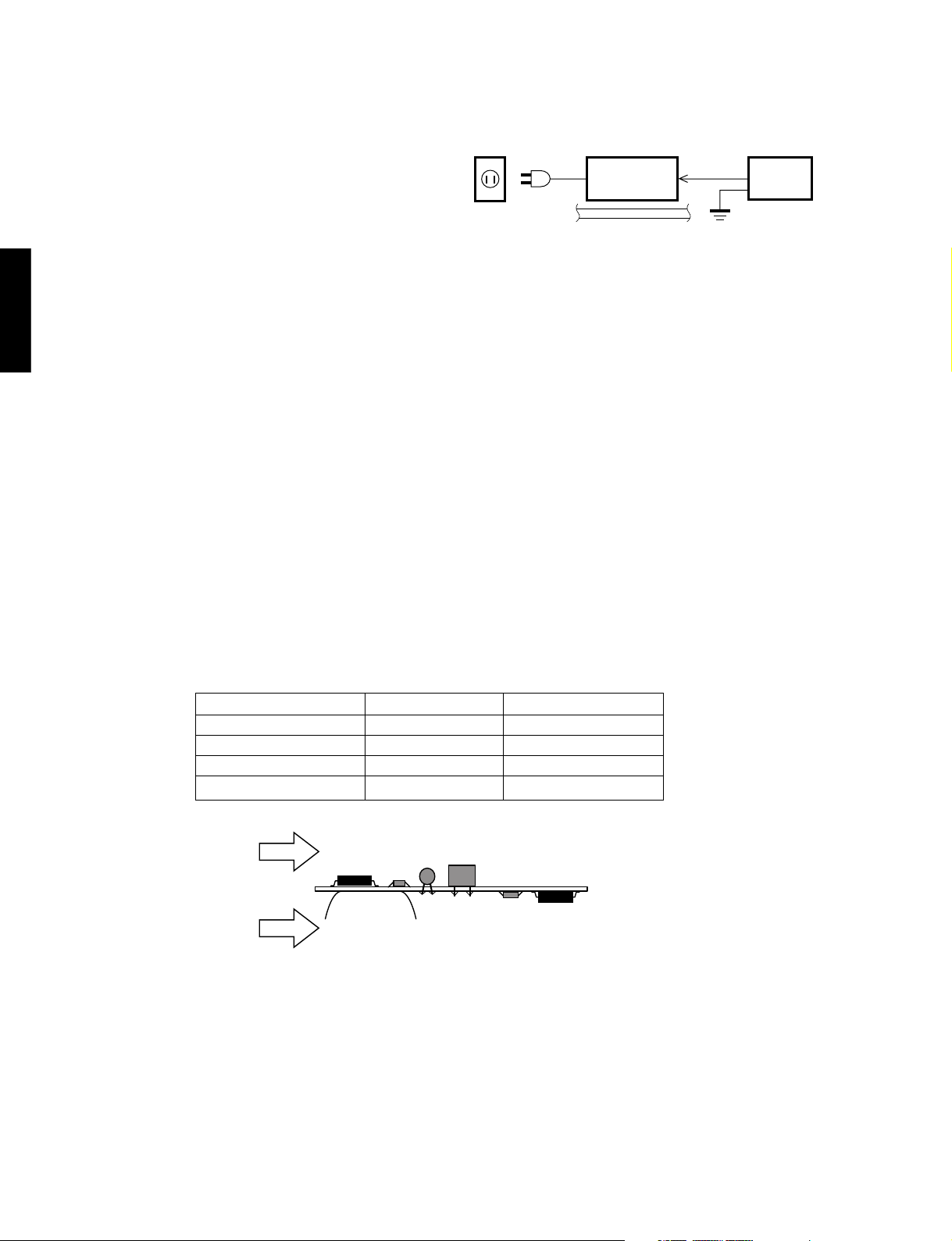
2. Leakage Current Measurement (For 120V Models Only)
● Meter impedance should be equivalent to 1500 ohms
DVD-S559
WARNING: CHEMICAL CONTENT NOTICE!
The solder used in the production of this product contains LEAD. In addition, other electrical/electronic and/or plastic (where
applicable) components may also contain traces of chemicals found by the California Health and Welfare Agency (and possibly
other entities) to cause cancer and/or birth defects or other reproductive harm.
DO NOT PLACE SOLDER, ELECTRICAL/ELECTRONIC OR PLASTIC COMPONENTS IN YOUR MOUTH FOR ANY REASON
WHATSOEVER!
Avoid prolonged, unprotected contact between solder and your skin! When soldering, do not inhale solder fumes or expose eyes to
solder/flux vapor!
If you come in contact with solder or components located inside the enclosure of this product, wash your hands before handling
food.
Components having special characteristics are marked Z
and must be replaced with parts having specifications equal
to those originally installed.
When service has been completed, it is imperative to verify
that all exposed conductive surfaces are properly insulated
from supply circuits.
shunted by 0.15µF.
WALL
OUTLET
● Leakage current must not exceed 0.5mA.
● Be sure to test for leakage with the AC plug in both
polarities.
EQUIPMENT
UNDER TEST
INSULATING
TABLE
AC LEAKAGE
TESTER OR
EQUIVALENT
About Lead Free Solder
The P.C.B.s installed in this unit are soldered using the following solder.
Side A Side B
DVD P.C.B. Lead Free Solder Lead Free Solder
POWER P.C.B. – Lead Free Solder
OPERATION 1 P.C.B. – Lead Free Solder
OPERATION 2 P.C.B. – Lead Free Solder
Side A
Side B
Among some types of lead free solder currently available, it is
recommended to use one of the following types for the repair
work.
• Sn + Ag + Cu (tin + silver + copper)
• Sn + Cu (tin + copper)
• Sn + Zn + Bi (tin + zinc + bismuth)
SMT
Solder Dip
MI
REFLOW
FLOW
Process
Process
Caution:
1. As the melting point temperature of the lead free solder is
about 30°C to 40°C (50°F to 70° F) higher than that of the
lead solder, be sure to use a soldering iron suitable to each
solder.
2. If lead solder must be used, be sure to remove lead free solder
from each terminal section of the parts to be replaced and
from the area around it completely before soldering, or make
sure that the lead free solder and lead solder melt together
fully.
2
Page 3

DVD-S559
WARNING: Laser Safety
This product contains a laser beam component. This component may emit invisible, as well as visible radia-tion, which may cause eye
damage. To protect your eyes and skin from laser radiation, the following pre-cautions must be used during servicing of the unit.
1) When testing and/or repairing any component within the product, keep your eyes and skin more than 30 cm away from the laser pick-up
unit at all times. Do not stare at the laser beam at any time.
2) Do not attempt to readjust, disassemble or repair the laser pick-up, unless noted elsewhere in this manual.
3) CAUTION : Use of controls, adjustments or perform-ance of procedures other than those specified herein may result in hazardous
radiation exposure.
Laser Emitting Conditions:
1) When the Top Cover is removed, and the STANDBY/ ON SW is turned to the “ON” position, the laser compo-nent will emit a beam for
several seconds to detect if a disc is present. During this time (5–10 sec.) the laser may radiate through the lens of the laser pick-up unit.
Do not attempt any servicing during this period!
If no disc is detected, the laser will stop emitting the beam. When a disc is loaded, you will not be exposed to any laser emissions.
2) The laser power level can be adjusted with the VR on the pick-up PWB, however, this level has been set by the factory prior to shipping
from the factory. Do not adjust this laser level control unless instruction is provided elsewhere in this manual. Adjustment of this control
can increase the laser emission level from the device.
DVD-S559
Laser Diode Propeties
Type: Semiconductor laser GaAlAs
Wave length: 650 nm (DVD)
780 nm (VCD/CD)
Output Power: 5 mW (DVD/VCD/CD)
Beam divergence 60 degree
VARO! : AVATTAESSA JA SUOJALUKITUS OHITETTAESSA
OLET ALTTIINA NÄKYMÄTTÖMÄLLE LASERSÄTEILYLLE. ÄLÄ KATSO SÄTEESEEN.
VARNING! : OSYNLIG LASERSTRÅLNING NÄR DENNA DEL
ÄR ÖPPNAD OCH SPÄRREN ÄR URKOPPLAD.
BETRAKTA EJ STRÅLEN.
WARNING
The use of optical instruments with this product will increase eye hazard.
Repair handling should take place as much as possible with a disc loaded inside the player.
:VISIBLE AND INVISIBLE LASER RADIATION WHEN OPEN. AVOID EXPOSURE TO BEAM
CAUTION
:SICHTBARE UND UNSICHTBARE LASERSTRAHLUNG WENN ABDECKUNG GEÖFFNET NICHT DEM STRAHL AUSSETSEN
VORSICHT
:SYNLIG OG USYNLIG LASERSTRÅLING VED ÅBNING UNDGÅ UDSÆTTELSE FOR STRÅLING
ADVARSEL
:SYNLIG OCH OSYNLIG LASERSTRÅLNING NÄR DENNA DEL ÄR ÖPPNAD BETRAKTA EJ STRÅLEN
VARNING
:AVATTAESSA OLET ALTTIINA NÄKYVÄLLE JA NÄKYMÄTTÖMÄLLE LASER SÄTEILYLLE, ÄLÄ KATSO SÄTEESEEN
VARO !
:RADIACIÓN LÁSER VISIBLE E INVISIBLE AL ESTAR ABIERTO. EVITAR EXPOSICIÓN AL RAYO.
CUIDADO
CAUTION VISIBLE AND INVISIBLE LASER RADIATION
ADVARSEL SYNLIG OG USYNLIG LASERSTRÅLING
ADVARSEL SYNLIG OG USYNLIG LASERSTRÅLING
VARNING SYNLIG OCH OSYNLIG LASERSTRÅLNING
VARO! AVATTAESSA OLET ALTTIINA NÄKYVÄLLE
VORSICHT SICHTBARE UND UNSICHTBARE
DANGER VISIBLE AND INVISIBLE LASER RADIATION
ATTENTION RAYONNEMENT LASER VISIBLE ET
WHEN OPEN. AVOID EXPOSURE TO BEAM.
VED ÅBNING. UNDGÅ UDSÆTTELSE FOR
STRÅLING.
NÅR DEKSEL ÅPNES. UNNGÅ
EKSPONERING FOR STRÅLEN.
NÄR DENNA DEL ÄR ÖPPNAD. BETRAKTA
EJ STRÅLEN.
JA NÄKYMÄTTÖMÄLLE LASER SÄ
TEILYLLE. ÄLÄ KATSO SÄTEESEEN.
LASERSTRAHLUNG WENN ABDECKUNG
GEÖFFNET. NICHT DEM STRAHL
AUSSETSEN.
WHEN OPEN. AVOID DIRECT EXPOSURE
TO BEAM.
INVISIBLE EN CAS D'OUVERTURE.
EXPOSITION DANGEREUSE AU FAISCEAU
3
Page 4
DVD-S559
Warning for power supply
The primary side of the power supply carries live mains voltage when the player is connected to the mains even when the
player is switched off !
This primary area is not shielded so it is possible to touch copper tracks and/or components when servicing the player.
Service personnel have to take precautions to prevent touching this area or components in this area.
Note:
The screws on the DVD mechanism may never be touched, removed or re-adjusted.
Handle the DVD mechanism with care when the unit has to be exchanged!
The DVD mechanism is very sensitive for dropping or giving shocks.
■ PREVENTION OF ELECTROSTATIC DISCHARGE
DVD-S559
The laser diode in the DVD mechanism may be damaged due to static electricity from clothes or the human body. Use caution to
prevent electrostatic damage when servicing or handling the DVD-mechanism.
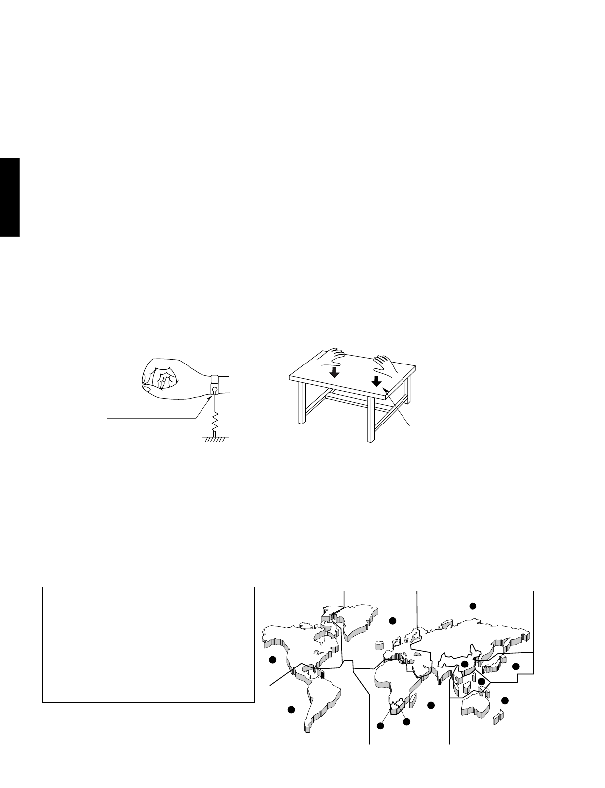
1. Grounding for electrostatic damage prevention
Some devices, such as the DVD player, use an optical pickup (laser diode) that will be damaged by static electricity in the working
environment. Only attempt service after ensuring that all grounding procedures have been completed.
1. Worktable grounding
Put a grounded conductive material (sheet) or iron sheet on the area where the optical pickup is placed.
2. Human body grounding
Use an anti-static wrist strap to discharge the static electricity from your body.
Anti-static wrist strap
1MΩ
Conductive material
(sheet) or steel sheet
2. Handling Precautions for DVD mechanism
1. Handle the DVD mechanism gently, as it is an extremely high-precision assembly.
2. The flexible cable lines may break if an excessive force is applied to it. Use caution when handling the cable.
3. The semi-fixed resistor for laser power adjustment should not be adjusted. Do not turn the resistor.
■ LOCALE MANAGEMENT INFORMATION
Locale Management Information : This DVD player is designed and manufactured to respond to the Locale Management Information that
is recorded on a DVD disc. If the Locale number described on the DVD disc does not correspond to the Locale number of this DVD
player, this DVD player cannot play this disc.
This product incorporates copyright protection
technology that is protected by method claims of
certain U.S. patents and other intellectual property
rights owned by Macrovision Corporation and other
rights owners. Use of this copyright protection
technology must be authorized by Macrovision
Corporation, and is intended for home and other limited
viewing uses only unless otherwise authorized by
Macrovision Corporation. Reverse engineering or
disassembly is prohibited.
2
1
4
2
5
5
5
6
3
2
4
4
Page 5

■ FRONT PANEL
■ REAR PANEL
DVD-S559
DVD-S559
■ REMOTE CONTROL
DVD
WG11920
5
Page 6
DVD-S559
■ SPECIFICATIONS
● RGB (SCART) output
Output level ........................................ 0.7 Vp-p (75 ohms)
Connection ................................................ Euroconnector
● Component video output
Y (luminance) - Output level.... 1 Vp-p (75 ohms)(Green)
Pb/Cb (color) - Output level..... 0.7 Vp-p (75 ohms)(Blue)
Pr/Cr (color) - Output level ....... 0.7 Vp-p (75 ohms)(Red)
Connection ................................................................ RCA
DVD-S559
● S-video output
Y (luminance) - Output level.................1 Vp-p (75 ohms)
C (color) - Output level .................. 286 mVp-p (75 ohms)
Connection .............................. S-video (Mini, DIN, 4 pins)
● Video output
Output level ........................................... 1 Vp-p (75 ohms)
Connection ................................................................ RCA
● General
System ............................................................ DVD player
Power requirements...................AC 220–240 V, 50/60 Hz
Power consumption ................................................... 7 W
Power consumption (standby) ............................... 0.7 W
Weight ............................................... 1.8 kg (3 lbs. 15 oz.)
Dimensions (W x H x D) ....... 435 mm x 61 mm x 213 mm
(17-1/8” x 2-3/8” x 8-3/8”)
Finish................................................................ Black color
Silver color
● Accessories
Audio/video cable x 1
Power cable x 1
Remote control x 1
AA/R6 dry cell batteries x 2
* Specifications subject to change without notice.
● Audio output (1 stereo pair)
Output level ....................................... During audio output
200 mVrms (1 kHz, -20 dB)
Number of channels........................................................2
Connection ................................................................ RCA
● Digital audio characteristics
Frequency response ..... 4 Hz to 44 kHz (DVD fs: 96 kHz)
S/N ratio ................................................................. 115 dB
Dynamic range ...................................................... 101 dB
Total harmonic distortion ................................. 0.0023 %
● Digital output
Coaxial digital output................................................RCA
IEC60958 for CDDA/LPCM
IEC61937 for MPEG 1/2,
Dolby Digital and DTS
G ....... European model
Manufactured under license from Dolby
Laboratories.
“Dolby” and the double-D symbol are trademarks
of Dolby Laboratories.
“DTS” and “DTS Digital Out” are trademarks of
Digital Theater Systems, Inc.
DivX and associated logos are trademarks of
DivXNetworks, Inc and are used under license.
This product incorporates copyright protection technology that is
protected by method claims of certain U.S. patents and other
intellectual property rights owned by Macrovision Corporation and
other rights owners. Use of this copyright protection technology must
be authorized by Macrovision Corporation, and is intended for home
and other limited viewing uses only unless otherwise authorized by
Macrovision Corporation. Reverse engineering or disassembly is
prohibited.
6
Page 7
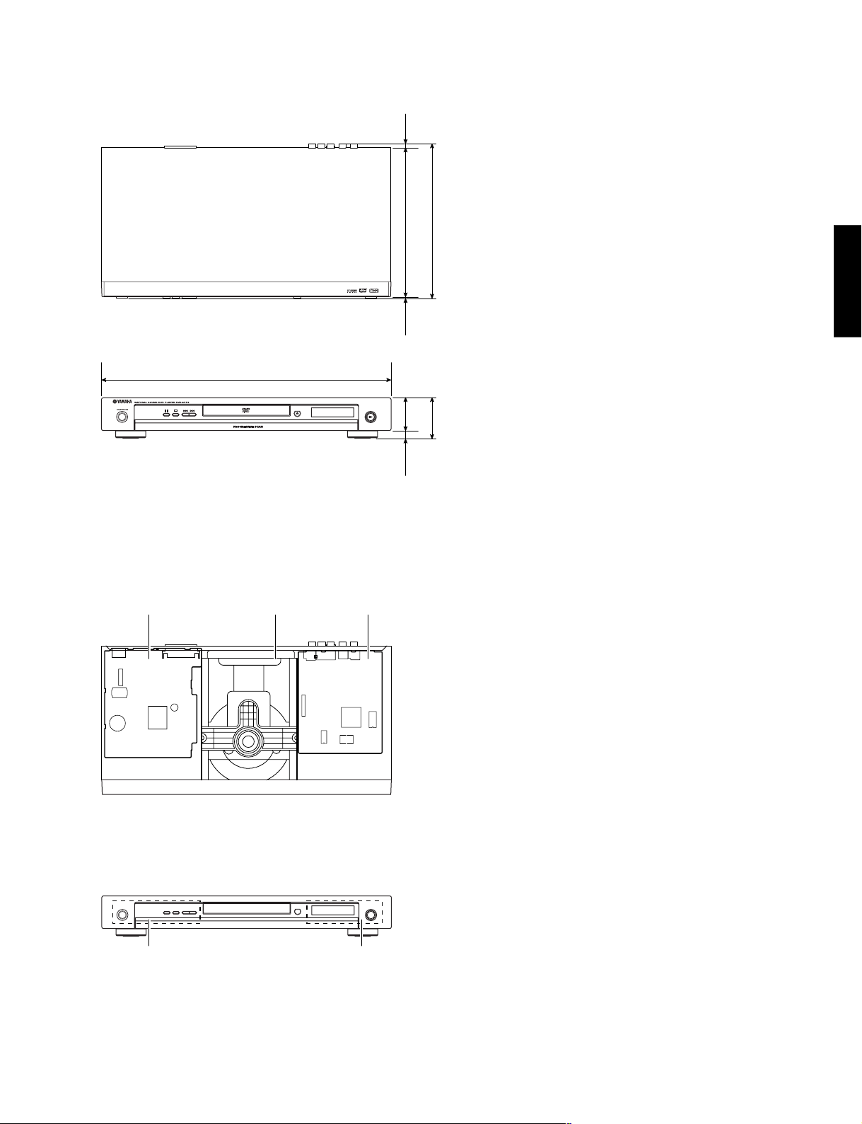
■ DIMENSIONS
6
DVD-S559
(1/4”)
435 (17-1/8")
■ INTERNAL VIEW
1 2 3
2
48
13
213 (8-3/8”)
205 (8-1/16”)
(1/16”)
)
61
1-7/8”
(
(2-3/8”)
(1/2”)
DVD-S559
1 POWER P.C.B.
2 DVD Mechanism Unit
3 DVD P.C.B.
5 4
4 OPERATION 1 P.C.B.
5 OPERATION 2 P.C.B.
7
Page 8

DVD-S559
■ REPAIR NOTES
• Repair Tips
None of the components of the following units can be supplied separately.
Each unit must be replaced as a whole in case of a failure.
• DVD Mechanism Unit
• POWER P.C.B.
• DVD P.C.B.
• OPERATION 1 P.C.B.
• OPERATION 2 P.C.B.
• When replacing DVD Mechanism Unit
1. Removing the DVD Mechanism Unit
DVD-S559
2. Installing the DVD Mechanism Unit
NOTE
• Before your operation, please read “PREPARATION OF SERVICING” .
• Use the Lead Free solder.
• Manual soldering conditions
• Soldering temperature: 320 ± 20°C
• Soldering time: Within 3 seconds
• Soldering combination: Sn-3.0Ag-0.5Cu
• When Soldering/Removing of solder, use the draw in equipment over the Pick Up Unit to prevent the Flux smoke from it.
Before removing DVD P.C.B. connector (Ref CP2301), short circuit the position shown in Fig. 1 using a soldering iron. If
you remove the DVD Mechanism Unit with no soldering, the Laser may be damaged.
Remove all the soldering on the short circuit position after the connection of DVD P.C.B. connector (Ref CP2301).
DVD
Mechanism Unit DVD P.C.B.
Pick Up P.C.B.
CP2301
Short circuit using a
soldering iron.
Fig. 1
PREPARATION OF SERVICING
The laser diode used for a pickup head may be destroyed with external static electricity. Moreover, even if it is operating
normally after repair, when static electricity discharge is received at the time of repair, the life of the product may be
shortened. Please perform the following measure against static electricity, be careful of destruction of a laser diode at the
time of repair.
• Place the unit on a workstation equipped to protect against static electricity, such as conductive mat.
• Soldering iron with ground wire or ceramic type is used.
• A worker needs to use a ground conductive wrist strap for body.
8
Page 9

■ DISASSEMBLY PROCEDURES
• Remove parts in disassembly order as numbered.
• Disconnect the power cable from the AC outlet.
* How to manually eject the tray (Fig. 1)
a. Turn the player bottom up.
b. Move the slider in the direction indicated with a screw driver until the tray is ejected.
c. Gently pull the tray out.
DVD-S559
DVD-S559
Tray
Frame
Rear
a
c
Front
b
Screw Driver
Slider
Fig. 1
9
Page 10
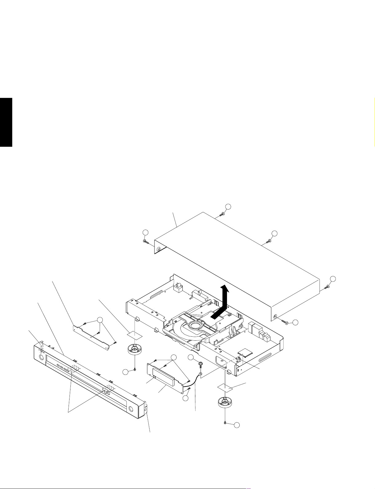
DVD-S559
1. Removal of Top Cabinet (Fig. 2)
a. Remove 5 screws (1).
b. Remove the Top Cabinet in the direction of arrow (A).
2. Removal of Front Cabinet . (Fig. 2)
a. Remove 2 screws (2).
b. Remove 2 Legs.
c. Remove 2 Sheet Earth. (Silver model)
d. Remove 1cable connection. [CP4002]
e. Remove 1 screw (3) and the cable. [CD602] (Silver model)
f. Unlock the Front Cabinet by releasing successively 4 snaps. (2 on the side and 2 on the bottom).
g. Remove the Front Cabinet.
DVD-S559
* The Sheet Earth once removed cannot be reused.
3. Removal of OPERATION 1 and OPERATION 2 P.C.B.s. (Fig. 2)
OPERATION 2 P.C.B.
Front Cabinet
Be sure to use a new Sheet Earth for replacement.
a. Remove 4 screws (4).
b. Remove the OPERATION 1 P.C.B..
c. Remove 1 cable connection. [CP603]
d. Remove 3 screws (5).
e. Remove the OPERATION 2 P.C.B..
1
Sheet Earth
(Silver model)
Top Cabinet
1
1
1
(A)
10
Snap
Snap
5
3
4
2
CP603
OPERATION P.C.B.
Snap
(Silver model)
Fig. 2
4
CD602
2
CP4002
Sheet Earth (Silver model)
1
Page 11

4. Removal of DVD Mechanism Unit. (Fig. 3)
a. Short circuit the position shown in Fig. 3 using a soldering iron. If you remove the DVD Mechanism Unit with no
soldering, the Laser may be damaged.
b. Remove 4 screws (6).
c. Remove 3 cable connections. [CP2301], [CP2302], [CP2303]
d. Remove the DVD Mechanism Unit.
DVD-S559
DVD Mechanism Unit
6
6
6
6
Short circuit using a soldering iron.
CP2301
CP2303
CP2302
Solder
Pick Up P.C.B.
DVD-S559
Fig. 3
11
Page 12

DVD-S559
5. Removal of POWER P.C.B.. (Fig. 4)
a. Remove 4 screws (7) and 2 screws (8).
b. Remove 3 cable connections. [CP503], [CP4001], [CP4003]
c. Remove the POWER P.C.B..
7
7
7
DVD-S559
7
POWER P.C.B.
CP503
8
8
CP4003
CP4001
Fig. 4
6. Removal of DVD P.C.B. (Fig. 5)
a. Remove 4 screws (9) and 4 screws (0).
b. Remove the DVD P.C.B. in the direction of arrow (B).
12
9
9
9
DVD P.C.B.
9
(B)
10
Fig. 5
Page 13

■ TROUBLESHOOTING
DVD-S559
Symptoms
No.
The power is not turned on.
1
An opening screen is not
2
displayed on the monitor.
(The FL display (V651) lights.
The mechanism does not work.)
Diagnosis Contents
“Check the voltage of AT+3.3V, -28V and FL-DC+/on the POWER P.C.B. Ass’y.”
Are wires of output connector CP502 on the POWER
P.C.B. Ass’y and CP4003 on the DVD P.C.B. Ass’y
disconnected or damaged ?
Check that the voltage at IC651-pin 10 (K 1) on the
OPERATION 1 P.C.B. Ass’y “becomes about 2.7V
when the POWER key (SW667, OPERATION 2
P.C.B. Ass’y)” is pressed and 0 V when it is released.
Check that the voltage at OS651-pin 1 (IR) on the
OPERATION 1 P.C.B. Ass’y is in the range between 0
and 3.3 V while receiving signals from the Remote
Control when any key on it is pressed.
Check the voltage of E+6.8V and SW+3.3V on the
POWER SUPPLY Unit.
Check the voltage of P.ON-H is about 2.8V on the
POWER SUPPLY Unit.
Check the voltage of IC4006-pin 2 is 1.8V on the
DVD P.C.B. Ass’y.
Is a resonator (X4001 : 27MHz) on the DVD P.C.B.
Ass’y oscillating ?
Is a signal input into IC4004-pin26 (PCE#) on the
DVD P.C.B. Ass’y ? (Is a signal “H” for 80 mS and
then “L” after the power is turned on ?)
➞ Communication with flash ROM.
Are the signals input into IC4005-pin 16 (DWE#), pin
19 (DCS#) and pin 38 (SDCLK) on the DVD P.C.B.
Ass’y ? (Is a signal fluctuating ?)
➞ Communication with SDRAM
Possible Defective Points
POWER P.C.B. Ass’y
Connector CP502 on the POWER P.C.B. Ass’y and
CP4003 on the DVD P.C.B. Ass’y.
Cable (From POWER P.C.B. Ass’y to DVD P.C.B.
Ass’y).
DVD-S559
Tact SW (SW660,662,664,665,667) on the
OPERATION 2 P.C.B. Ass’y.
(when operation of only the POWER key on the main
unit is not accepted)
Remote receiver section on the OPERATION 1 P.C.B.
Ass’y. (when operation of only the POWER key on
the Remote Control is not accepted)
POWER P.C.B. Ass’y.
1.8V Regulator IC (IC4006) on the DVD P.C.B. Ass’y.
Crystal resonator (X4001) on the DVD P.C.B. Ass’y.
DVD IC (IC4002), Flash ROM (IC4004) and SDRAM
(IC4005) on the DVD P.C.B. Ass’y.
A tray cannot be opened.
3
(An opening screen is
displayed on the monitor)
Is a signal output from IC4004-pin 28 (PRD#) on the
DVD P.C.B. Ass’y ?
(Is a signal fluctuating for several hundred mS after
the power is turned on ?)
Are the signals of IC4001-pin 5 (SDA) and pin 6
(SCL) on the DVD P.C.B. Ass’y fluctuating for one or
two seconds after the power is turned ?
Check the video signal path between DVD IC
(IC4002) on the DVD P.C.B. Ass’y and Video-out
(J8001) terminal.
Does the voltage of CP2302-pin 3 and pin 1 on the
DVD P.C.B. Ass’y change normally ?
SW-1-pin 3 (OPEN) on the DVD Mechanism Unit :
Tray is fully opened: “L”
SW-2-pin 5 (CLOSE) on the DVD Mechanism Unit :
Tray is fully closed: “L”
Is a LOAD-DRV signal reaching ?
Are the signals output from IC101-pin 36 and pin 37
(CN103-pin 1 and pin 2) on the DVD Mechanism
Unit ?
Pin 4: Approx. 45V during opening tray approx. 0V
during closing tray.
Pin 5: Approx. 0V during opening tray approx.
4.5V during closing tray.
Are wires of CP2302 and CP2303 on the DVD P.C.B.
Ass’y disconnected or damaged ?
Flash ROM (IC4004) on the DVD P.C.B. Ass’y.
EEPROM (IC4001) on the DVD P.C.B. Ass’y.
Video circuit after DVD IC (IC4002) on the DVD
P.C.B. Ass’y.
Tray SW on the DVD Mechanism Unit.
DVD IC (IC4002) on the DVD P.C.B. Ass’y.
DVD P.C.B. Ass’ y
FTS Driver IC (IC2301)
Connector CP2302 and CP2303 on the DVD P.C.B.
Ass’y.
Cable (From DVD P.C.B. Ass’y to DVD Mechanism
Unit).
13
Page 14

DVD-S559
No.
4
DVD-S559
5
Symptoms
Playback impossible
(no focusing)
Playback impossible
(Spindle does not turn)
Diagnosis Contents
Does the voltage of CP2301-pin 5 on the DVD
Mechanism Unit change by pressing the Inside switch
(SW2).
Are the signals output from IC2301-pin 9 (F+) and pin
8 (F-) on the DVD P.C.B. Ass’y ?
Does 650-nm LD emit light ?
Does a pickup lens move up / down ?
Does an actuator spring bend ?
Are plastic parts damaged ? Or is a shaft detached ?
Is the turntable detached or tilted ?
Is cable of CP2301 on the DVD P.C.B Ass’y
disconnected or damaged ?
Is signal output from IC4002-pin 42 (FOSO) on the
DVD P.C.B. Ass’y ? (Device control of about 1.4 V is
output usually. It is fluctuated by about ± 250 mV
with focus up / down.)
Are the signals output from IC2301-pin 10 (MOT
SPDL-), and pin 11 (MOT SPDL+)”
on the DVD P.C.B. Ass’y ?
Is IC2301-pin 33,34 (STBY) on the DVD P.C.B.
Ass’y fixed LOW ?
Is there any part detached from the spindle motor ?
Or Is there any foreign object lodged in it ?
Possible Defective Points
Inside switch (SW2) on the DVD Mechanism Unit.
FTS Driver IC (IC2301) on the DVD P.C.B. Ass’y.
Pickup on the DVD Mechanism Unit.
Mechanism section (motor) on the DVD Mechanism
Unit.
Connector CP2301 on the DVD P.C.B. Ass’y.
Cable (From DVD P.C.B. Ass’y to DVD Mechanism
Unit).
DVD IC (IC4002) on the DVD P.C.B. Ass’y.
FTS Driver IC (IC2301) on the DVD P.C.B. Ass’y.
Mechanism section (Spindle motor) on the DVD
Mechanism Unit.
Playback impossible
6
(Playback stops)
Picture disturbance during
7
playback (block noise, freeze,
other)
No sound (Picture is normal)
8
Are wires of CP2303 on the DVD P.C.B. Ass’y
disconnected or damaged ?
Is signal output from IC4002-pin 37 (DMSO) on the
DVD P.C.B. Ass’y ?
Does 650-nm LD deteriorate ?
If the voltage at each both ends of R2303 and R2305
on the DVD Mechanism Unit is 0.4 V or more, the
650-nm LD is definitely deteriorated.
Does 780-nm LD deteriorate ?
If the voltage at each both ends of R2302 and R2304
on the DVD Mechanism Unit is 0.4 V or more, the
780-nm LD is definitely deteriorated.
Are there scratches or dirt on the disc ?
Are there scratches or dirt on the disc ?
Is there a problem with the format of the disc ?
Check the waveform. IC4002-213pin (ALRCK),
214pin (ABCK), 215pin (ACLK), 217pin (ASDATA)
Is signal output from IC8004-pin 7 and pin 8 on the
DVD P.C.B. Ass’y ?
Connector CP2301 on the DVD P.C.B. Ass’y.
Cable (From DVD P.C.B. Ass’y to DVD Mechanism
Unit).
DVD IC (IC4002) on the DVD P.C.B. Ass’y.
650-nm LD deteriorated. (When playback of a DVD is
impossible)
780-nm LD deteriorated. (When playback of a CD is
impossible)
Disc
Disc
DVD IC (IC4002)
Audio Dac IC (IC8004) on the DVD P.C.B. Ass’y.
14
Page 15

ABCDEFGH
DVD-S559
■ BLOCK DIAGRAMS
1
OVERALL BLOCK DIAGRAM
2
5
11
R
L
21 PIN
CV
Y
U
V
S
CO
AUDIO OUT L/R
AV (SCART)
VIDEO
Y
P
B/CB
PR/C
S-VIDEO
DIGITAL OUT
COAXIAL
COMPONENT
R
POWER
• See page 27, 28 ➝
SCHEMATIC DIAGRAM
VIDEO
OUT
OPERATION 1
• See page 29 ➝
SCHEMATIC DIAGRAM
IC4002
16K EEPROM
MT1389FE/C2-L
OPERATION 2
• See page 29 ➝
SCHEMATIC DIAGRAM
2
KEY
SW660, 662,
664, 665, 667
KEY
SW663, 666
IR
3
IR RECEIVER (OS651)
IC2301
MOTOR DRIVE
LA6565-TE-L-E
FIP V651
HNV-08SS44T
IC651
FIP Driver IC
PT6315
IR
SERVO
RF
1.7
FP
LD
111
27MHz
228 229
MPEG BLOCK
RF AMP
SDA, SCL
MPEG-1/2
JPEG
VIDEO
DECODER
IC8004
AUDIO DAC 2CH IC
PCM1742KE/2K
11
D_AUDIO
AUDIO CODEC
108MHz
TV ENCODER
AUDIO_L/R
7.8 2.6 1.7
ZERO
4CH VIDEO DAC
ASPDIF
225
/URST
110
IC8003
AUDIO AMP IC
BA4560F-E2
VIDEO DRIVER 6CH IC
IC4003
RESET IC
BD5229G-TR
AUDIO_L/R
23
IC8002
MM1623BFBE
CVBS
VIDEO SW IC
SN74CBT3257PWR
21, 26
RGB
IC8001
S_VIDEO
COAXIAL
DVD
SERVO
4
POWER
• See page 27, 28 ➝
SCHEMATIC DIAGRAM
AC220V-240V
DVD LOADER
(DM4)
POWER
SUPPLY
P.CON+12V
P.CON+5V
P.CON+6V
P.CON+3.3V
AT+3.3V
AT+12V for mute
-28V
FLDC+/-
IC4004
16Mbit FLASH
S29AL016D70TFI020
IC4005
64Mbit SDRAM
K4S641632H-UC75
• See page 22–26 ➝
SCHEMATIC DIAGRAM
5
6
15
Page 16

ABCDEFGH
DVD-S559
1
DVD LOADER/MPEG BLOCK DIAGRAM
DVDDVD MECHANISM UNIT
• See page 22–26 ➝
SCHEMATIC DIAGRAM
DVD
LOADER
(DM-4)
D
IOA, V20
X4001
27MHz
IC4001
EEPROM
BR24L16FJ-WE2
A
C
IC4006
REG+1.8V
LM1117S-ADJ
A
2
RF, A, B, C, D, E, F, MDI1
SDA
OPU
LD_DVD, LD_CD
T+/-, F+/-,
3
SPINDLE/
STEPPING/
SLED
MOTOR
LOAD+/-,
MOT_SLED+/-,
MOT_SPDL+/-
A (or B)
Q2302-2305
LD DRIVE
E
IC2301
MOTOR DRIVE
LA6565-TE-L-E
LIMIT, TRIN, TROUT,
OPO, OP+/-
103 102
LDO1, LDO2
DMSO, FMSO,
TROPEN, TRCLOSE,
TRSO, FOSO,
STBY, V1P4
IC4002
MPEG/MICON/RF-AMP
MT1389FE/C2-L
SCL
A, C
110
111
225
/URST
IC4003
RESET IC
BD5229G-TR
IC8004
AUDIO DAC 2CH
PCM1742KE/2K
11
7.8
A
<VIDEO/AUDIO/FIP BLOCK>
IR
FP_DI, FP_DO, FP_SCK,
STB, FLDC+/-
R/CR, B/CB, G/Y, C/V
(4CH Video DAC)
VSEL1, I/XP,
LETTER, SQUEEZE
ASPDIF
ZERO
AUDIO_L/R
4
DAC_XCSO,
A0-A20, AD0-AD7,
/PRD,/PCE,/PWR
IC4004
A
5
16Mbit FLASH
S29AL016D70TFI020
MA0~MA11,
DQ0~DQ15,
/DCS. /DRAS, /DCAS,
/DWE, DBA0, DBA1,
SDCLK0, SDCKE, DQM0, DQM1
IC4005
64Mbit SDRAM
K4S641632H-UC75
A
SCK, SD,
ACLK, ABCK,
ALRCK, ASDAT0
A, D
A
.......AT+3.3V
B
.......P.CON+3.3V
C
.......+1.8V
D
.......P.CON+5V
E
.......P.CON+6V
F
.......AT+12V
G
.......P.CON+12V
H
.......-28V
16
6
Page 17

ABCDEFGH
DVD-S559
1
VIDEO/AUDIO/FIP BLOCK DIAGRAM
<DVD LOADER/MPEG BLOCK>
<21PIN/D-CONNECTOR BLOCK>
CVBS
R/CR, B/CB, G/Y, CVBS,
S_Y, S_C (6CH Video DAC)
2
IC8002
VIDEO DRIVER IC
MM1623BFBE
G/Y, B/CB, R/CR
SN74CBT3257PWR
D
IC8001
4CH BUS SW IC
R, G, B
D
Y, CB, CR
S_Y, S_C
CVB
U
S
Y
V
I/XP, LETTER,
SQUEEZE
S
VSEL1
S JACK (J8002)
VIDEO JACK (J8001)
3
VSEL1, SQUEEZE
AUDIO_L/R
VSEL1, I/XP,
LETTER, SQUEEZE
G
AUDIO_L/R
IC8003
AUDIO AMP IC
BA4560F-E2
L
AUDIO JACK (J8003)
ZERO
4
ASPDIF
OPERATION 1
FP_DI, FP_DO, FP_SCK, STB
5
FIP DRIVER IC
PT6315
IC651
A, H
MUTE Tr
GR1 – GR8,
P1–P16
COAXIAL
DRIVE
COA
COAXIAL (J8004)
F
R
D
FIP (V651)
A
.......AT+3.3V
B
.......P.CON+3.3V
C
.......+1.8V
D
.......P.CON+5V
E
.......P.CON+6V
F
.......AT+12V
G
.......P.CON+12V
H
.......-28V
8-BT-234GNK
FLDC+/-
A
IR
IR RECEIVER (OS651)
IR
6
17
Page 18

ABCDEFGH
DVD-S559
1
POWER/21 PIN BLOCK DIAGRAM
G_VIDEO
CP503
2
POWER CTL
STR-A6151M
PHOTO COUPLER
IC504
PS2561AL1-1-V (W)
IC502
VOLTAGE CTL
IC501
KIA431A-AT
(CP8001)
FFC
CONNECTOR
ASP/FS
P-H/I-L
_RGB-H
B_VIDEO
R_VIDEO
CVBS_VIDEO
AUDIO_R
AUDIO_L
P.CON +12V
Q8101, Q8102
21 PIN CTL
AT+3.3V
Q8104, Q8105
DVD_RGB_H_OUT
21 PIN CTL
BLANKING_OUT
3
Q510
P.CON +12V SW
Q515
P.CON +5V SW
J8101
21PIN CONNECTOR
AV (SCART)
AT+12V for mute
P.CON+12V
P.CON+5V
SWITCHING
AC IN
TRANS
T501
4
5
6V REG
IC503
PQ070XF01SZH
Q505
P.CON SW
Q504
FL + P.CON SW
Q502
-28V P.CON SW
P.CON+6V
P.ON-H
AT+3.3V
FL DC -
FL DC +
-28V
18
6
Page 19

■ WIRING DIAGRAM
ABC DEF GH
DVD-S559
8
7
1234
E
CVBS/Y/U/V
J8001
H1H2EH1H2
56
H
2
1
E
COAXIAL
J8004
6
OPE1 PCB
PCB270
DEE029
CP602
CD603
6
CD501_8
6
5
5
4
4
3
3
2
2
1
16
AT+3.3V
J501
SW2
5
OPE2 PCB
PCB280
DEE037
STOP
+SKIP
PAUSE/-SKIP
POWER
SW1
4
AC220V-240V_50Hz/60Hz
3
S80X
CP603
1
2
3
4
5
6
SW2
STOP
+SKIP
PAUSE/-SKIP
POWER
SW1
21PIN CONNECTOR
J8101
NC
NC
NC
NC
1
2
3
4
5
12
NN
L
2
POWER PCB
PCB240
DPE004
NC
OS651
1
5
7
9
11
13
15
17
19
21 3
VoutB+GND
123
CLK
DI (M to F)
STB
DO (F to M)
IR
V+3E
DGND
DGND
FLDC+
-28V
FLDC-
G/Y
GND
B/CB
GND
R/CR
RGB-H
FS
CVBS
GND
AUDIO L
GND
220
4
6
8
10
12
14
16
18
AUDIO R
GND
P.CON+12V
AT+12V for MUTE
GND
P.CON+5V
P.CON+6V
GND(M)
P.CON+3.3V
AT+3.3V
P.ON-H
GND(D)
FL DC-
FL DC+
-28V
CP601
CP503
CP502
CD601
1
1
2
2
3
3
4
4
5
5
6
6
7
7
8
8
9
9
10
10
11
11
CD8001
12
12
11
11
10
10
9
9
8
8
7
7
6
6
5
5
4
4
3
3
2
2
1
1
1
2
3
4
5
6
7
8
9
10
11
12
13
14
CP4001_1
1
V+3D
2
RXD
3
TXD
CP4002
CLK
1
1
DI (M to F)
2
2
3
4
5
6
7
8
9
10
11
1
2
3
4
5
6
7
8
9
10
11
12
3
DO (F to M)
4
5
6
7
8
9
10
11
CP8001
1
2
3
4
5
6
7
8
9
10
11
12
CP4003
1
P.CON+12V
2
AT+12V for MUTE
3
4
P.CON+5V
5
P.CON+6V
6
7
P.CON+3.3V(AT)
8
9
10
11
12
13
14
STB
IR
V+3E
DGND
DGND
FLDC+
-28V
FLDC-
G/Y
GND
B/CB
GND
R/CR
RGB-H
FS
CVBS
GND
AUDIO L
GND
AUDIO R
GND
GND
GND(M)
AT+3.3V
P.ON-H
GND(D)
FL DC-
FL DC+
-28V
Y/C SEPA
J8002
34
12
56
DVD PCB
PCB130
DME025
H1H2
23
1
E
DVD AUDIO OUT
J8003
CD2001
CP2301
24
FOCS RTN
FOCS DRV
TRKG RTN
TRKG DRV
GND
LD_DVD(650)
PD/GND
LD_CD(780)
GND
VR780(CD)
VRCOM
VR650(DVD)
VRF(RF_OUT)
SW1(DVD/CD)
SPD+
SPD-
SLD+
SLD-
LIMIT SW
SW(GND)
CLOSE
GND(D)
OPEN
24
23
23
22
22
21
21
20
20
NC
19
19
18
18
17
17
16
16
15
15
14
14
13
13
12
12
11
11
A
10
10
B
9
9
8
8
7
7
C
6
6
D
5
5
E
4
VCC
VS
GND
LD- LD-
4
3
3
2
2
F
1
1
CP2303
1
1
2
2
3
3
4
4
5
5
6
6
CP2302
1
2
3
4
5
24
23
22
21
20
19
18
17
16
15
14
13
12
11
10
9
8
7
6
5
4
3
2
1
1
2
3
4
5
6
FOCS RTN
FOCS DRV
TRKG RTN
TRKG DRV
NC
GND
LD_DVD(650)
PD/GND
LD_CD(780)
GND
VR780(CD)
VRCOM
VR650(DVD)
A
B
VRF(RF_OUT)
SW1(DVD/CD)
C
D
E
VCC
VS
F
GND
SPD+
SPD-
SLD+
SLD-
LIMIT SW
SW(GND)
CLOSE
GND(D)
OPEN
LD+LD+
DVD
DRIVE
DM-4
OPTICAL PICK-UP
SPINDLE MOTOR
SLED,LOADING MOTOR
FG SENSER
8
7
6
5
4
3
2
1
CAUTION
:SINCE THESE PARTS MARKED BY
CRITICAL FOR SAFETY,USE ONES
DESCRIBED IN PARTS LIST ONLY
ARE
ATTENTION
:LES PIECES REPAREES PAR UN ETANT
DANGEREUSES AN POINT DE VUE SECURITE
N'UTILISER QUE CELLS DECRITES
DANS LA NOMENCLATURE DES PIECES
OF PRINTING AND SUBJECT TO CHANGE WITHOUT NOTICE
THE TIMETHIS INTERCONNECTION DIAGRAM IS THE LATEST ATNOTE:
1
ABC DEF GH
19
Page 20

ABCDEFGH
DVD-S559
■ PRINTED CIRCUIT BOARDS
1
2
FOR INFORMATION ONLY (NO REPLACEMENT COMPONENT PARTS WILL BE AVAILABLE)
DVD (TOP VIEW) DVD (BOTTOM VIEW)
Lead Free Solder Used Lead Free Solder Used
To CP601 of OPERATION1 P.C.B.To S801X of POWER P.C.B.
IC4005
C4082
R4005
C4072
C4005
C4073
R2307
R4070
R4015
C4007
R2306
CP2301
C4012
R4016
C4001
C2321
Q2307Q2306
R4071
C4021
R4002
R2323
Q2305
R2321
NR4002
C4009
C2320
C4088
129193
R4018
R4017
C4008
R2322
Q2303
C4024
C2306
W819
C4023
C2314
R2320
W817
C2301
R4019
C4002
Q2304
C4003
Q2302
C4084
C4064
C4062
C4025
W809
R2330
R2327
IC4001
C4030
R4012
R2328
R2326
R2325
C4057
C4091
R4011
W820
R4003
R4051
R4087
R2318
CP2303
C4022
W844
C2307
R2316
R2317
C2325
IC2301
R4007
C4054
R4013
R4014
NR4001
R4036
IC4004
C4081
R4026
C2313
C2305
R2338
C4086
C2312
R2312
C4076
C4077
CP4001_1
C4090
R4035
R4034
R2337
R2311R2313
R2310
R2335
C2311
C4114
C4079
IC4003
C4115
C4078
P230
C
C4074
2
00
CP4
2
C2308
R4084
R2332
R2333
C2323
C2322
R2342
R2331
R2319
R2329
C2309
C4075
R2334C2310
DME025A
C4116
R8070
R4047
R4046
Q8010
R4043
B8003
W811
R4067
R4024
C4103
C4105
R8046
R4064
X4001
B4002
W815
R4050
C4046
R4069
R4065R4066
W816
R4068
W812
W814W813
C4047
W832
R4054
C4048C4049
C4045
C4104
C4102
C4034
R4022
C4040
W833
R4001
C4044
W829
R4027
R4025
C4042
W847
C4061
C4060
R4052
C4043
C4093
C4041
C4035
C4033
W848
W834
C4063
C4053
C4050
C4032
C4098 C4099
C4066
R4062
C8014
C8015
B8004
C8036
R8037
Q8005
R8038 R8036
R8039
R8040
W824
C8042
R8026
R8023
B8002
R8027
R8017
R8024
R8016
R8028
R8029
R8076
R8084
R8078
C8078
Q8018
C8077
R8085 R8080
R8083
B8001
R8018
Q8020
R8079
Q8019
C8038
Q8021
C8024
C8025
R8081
C8010
C8023
R8077
R8074
R8073
R8082
B8007
C8070
C8073
R8056
C8022
Q8014
C8026
R8060
Q8013
B8006
CP8001
R8063
C8067
C8072
C8069
R8067
R8051
R8014
IC8003
D8005
C4110
R8059
C8016
C8057
R8048
R8049
R8061
R8066
R8069
R8054
C8062
R8035
J8002
J8004
C8021
R8021
3
COAXIAL
DIGITAL OUT
S-VIDEO
)
R
/C
R
/P
B
/C
VIDEO OUT
B
COMPONENT
(Y/P
J8001
4
VIDEO
AUDIO
OUT L/R
J8003
W866
C8059
C8058
C8053
C8046
C8056
W870
Q8016
IC8002
C8017
C8051
R8057
C8008
C8063
D8007
C8066
C8005
C8004
C8002
C8006
C8003
C8001
IC8001
IC8004
C8061
R8065
C8075
C8068
R8044
C8074
C8076
C4085
R4061
C4067
C4071
16 5
C4101
C4026
R4020
C4031 C4028
C4027
C4017
C4016
C4015
C4014
S802Y
C4100
W852
B4001
R4033
R4044
W853
C4052
C4096
IC4006
C4094
R4037 R4039
W850
C4112
C4109
C4039
CP4003
B4007
W851
S802X
C2302
C4013
C4095
C4068
C2303
IC4002
C4019
C4080
Q2301
R4082
C4020
R2309
R2308
DME025A
To CP503 of POWER P.C.B. To CP502 of POWER P.C.B. To DVD MECHANISM UNIT
5
20
6
Page 21

ABCDEFGH
DVD-S559
1
POEWR (INSERTED PARTS)
SOLDER SIDE
POEWR (CHIP MOUNTED PARTS)
SOLDER SIDE
Lead Free Solder Used
C516
L501
AC IN
2
To PC4001 of
DVD P.C.B.
3
AV (SCART)
J501
J8101
C8112
C8113
C8114
W026
C8115
L8101
W035
W027
R8103
W029
R8120
R8105
W032
W031
C
R8101
P
5
W030
03
R546
W021
D517
C502_2
R524
W025
R525
C535
FH502FH501 F501
D534
W012
C531
L503
503
IC
C536
D532
C527
W023
W036
W024
W814
W821
S801X
Q515
C526
R542
D512
W811
L505
W019
R540
Q510
W817
C538
CP502
RISK
REPLACE
D510
C521_1
C523
W015
W016
R503
W018
D502
OF
W017
FIRE
AS
MARKED
W013
W815
D531
D505
C522_1
D503
D506
W008
W007
.
D527
28
5
D
D525
C533
D535
IC502
Q502
D511
R
51
T501
1
R539
R505
D519
R502
W010
R510_1
R529
W011
C514
D515
C520
C511
C517
C506
C509
IC501
C519
Q504
C528
B501
C505
C513
D513
D520
R528
W003
D523
D536
D508
C515_1
D509
W006
D516
W002
W004
W001
R530
D533
R512_1
R513
C540
D522
DPE004B
R534
W005
D521
R517
C518
R507
IC504
R514
R527
C8116
C8111
C8107
R8110
R8111
R8112
Q8105
R8109
R8113
R8102
C8105
R8108
D8101
R8114
C8106
Q8104
Q8102
R8115
R8104
Q8101
R545
R526
C8101
C501
R519
Q505
R541
R509
R547
Q509
C507
Q511
R543
C541
R518
R504
C508
Q512
C503
Q513
Q503
R515
R506
R516
DPE004B
R544
R536
R531
R537
R523
Q501
Q506
R538
To CP4003 of DVD P.C.B.To CP8001 of DVD P.C.B.
4
OPERATION 1 (INSERTED PARTS)
SOLDER SIDE
To CP4002 of DVD P.C.B
W005
CP603
D656
D657
D658
D659
W006
V651
CP601
D669
W004
W002
W007
W009
R666
W805
W008
OS651
C674
)
SW666
Silver
model
DEE029A
5
CD602
W001
#
SW663
W003
OPERATION 2 (INSERTED PARTS)
SOLDER SIDE
SW662
SW664
SW665
SW660
$› & *
CP602
DEE037A
STANDBY/ON
SW667
OPERATION 1 (CHIP MOUNTED PARTS)
SOLDER SIDE
Lead Free Solder Used
R654
R662
C675
C601
C602
C603
1
IC651
34
12
C658
23
C659
R658
C651
DEE029A
R656
R657
R655
R651
C676
R652
R653
OPERATION 2 (CHIP MOUNTED PARTS)
SOLDER SIDE
DEE037A
C660_1
Lead Free Solder Used
6
21
Page 22

DVD-S559
■ SCHEMATIC DIAGRAMS
FOR INFORMATION ONLY (NO REPLACEMENT COMPONENT PARTS WILL BE AVAILABLE)
ABCDE F GH
FROM/TO LOADER/MOTOR DRIVE
8
A
B
C
D
E
F
MDI1
LDO1 SQUEEZE
LDO2
V1P4
DMSO
FMSO
TRCLOSE G/Y
TROPEN
PWMOUT1
7
6
5
4
3
2
1
22
TRSO
FOSO
TROUT SD
TRIN
STBY
V20
LIMIT
IOA ALRCK
DEICG
RF
OPO
OP+
OP- ASPDIF
FROM/TO MEMORY
MA0
MA1
MA2
MA3
MA4
MA5
MA6
MA7
MA8
MA9
MA10
MA11
SDCKE
SDCLK
DBA0
DBA1
DCS#
DRAS#
DCAS#
DWE#
DQM0
DQM1
DQ0
DQ1
DQ2
DQ3
DQ4
DQ5
DQ6
DQ7
DQ8
DQ9
DQ10
DQ11
DQ12
DQ13
DQ14
DQ15
A0
A1
A2
A3
A4
A5
A6
A7
A8
A9
A10
A11
A12
A13
A14
A15
A16
A17
A18
A19
A20
AD0
AD1
AD2
AD3
AD4
AD5
AD6
AD7
PWR#
PCE#
PRD#
D
A
B
C
RF
E
F SQUEEZE
MDI1
LDO2
LDO1 I/XP
V20
V1P4
C4007
0.1 B
C4008
OPO MA9
OP- MA11
OP+ SDCKE
DMSO SDCLK
FMSO
TROPEN
PWMOUT1
TRSO
FOSO MA3
C4001 0.0022 B
V1P4
C4002 270P CH
C4003 150P CH
ADIN
TROUT DBA1
TRIN RXD
STBY DBA0
(ENDM)
TRCLOSE
A2
A3
A4 DWE#
A5
A6 DQM1
A7 DQ8
A8
A18 DQ9
A19 DQ10
SDA
SCL V+3E
(V+3D)
V+3
ABCDE F GH
C4005
0.1 B
Point 1
500 µs
MPEG/MICON/RF-AMP SCHEMATIC DIAGRAM
(DVD PCB 1/5)
SD
V+3
V1P4
100K
R4022
C4028
1.5
252
1.0
TP4016
A15
C4033
0.001 B
0.1 B
C4101
0.0
0.0
0.0
250251
NC
OSP
HIGHA5 (PU)
HIGHA6 (PU)
2.5
1.2
1.4
TP4017
TP4018
A14
A13
A12
C4034
0.1 B
C4031
2.0
0.0
NC
RFGND
CRTPLP
253
OSN
254
RFGC
255
IREF
256
AVDD3
HIGHA3 (PU)
HIGHA4 (PU)
DVDD3
1.4
3.3
TP4019
TP4020
C4030
0.1 B
A11
IOCE#
TP4096
0.033 B
1.5
HRFZC
65
66
67
68
HIGHA2 (PU)
1.2
A10
V+3RF
15K
R4020
C4027
0.1 B
C4026
0.1 B
1.2
1.0
3.3
255256
253254
110
AGND
DVDA
3
DVDB
4
DVDC
5
DVDD
6
DVDRF[P
DVDRF[N
MA
MB
MC
MD
111213141516171819 22021222324
SA
SB
SC
SD
CDFON
CDFOP
TNI
TPI
MIDI1
MIDI2
LDO2
LDO1
SVDD3
CSO/RFOP
2526272829
RFLV/RFON
SGND
V2REFO
V20
VREFO
30313233343536373839
FEO
TEO
TEZIS[LV
OP_OUT
OP_INN
OP_INP
DMO
FMO
TROPENPWM
PWMOUT1/V_ADIN9
40414243444546474849
TRO
FDO
USB_VSS
NC
NC
USB_VDD3
FG/V_ADIN8 (PU)
TDI/V_ADIN4 (JTAG)
TMS/V_ADIN5 (JTAG)
TCK/V_ADIN6 (JTAG)
50
TDO/V_ADIN7 (JTAG)
51525354
DVDD18
IOA2 (PU)
IOA3 (PU)
IOA4 (PU)
55
IOA5 (PU)
56575859
IOA6 (PU)
IDA7 (PU)
HIGHA0 (PU)
IOA18 (PU)
6061626364
IOA19 (PU)
DVSS
APLLCAP
0.0
APLLVSS
65 66 67 68 69770 71 72 73 74 75 76 77 78 79880 81 82 83 84 85 86 87 88 89990 91 92 93 94 95 96 97 98 99
3.33.33.33.33.33.33.33.33.33.33.33.33.33.33.33.33.33.33.33.33.33.33.33.33.33.33.33.33.33.33.33.33.33.33.33.33.33.33.33.33.33.33.33.33.33.33.33.33.33.33.33.33.33.33.33.33.33.33.33.33.33.33.33.33.3
2.9
3.3
TP4015
C4025
0.1 B
PWR#
A16
IOWR#
TP4014
R4012
C4021
3.3V
C4022
TP4012
TP4013
10K
TP4010
TP4011
0.1 B
C4023
0.0
1.2
2.1
0.9
0.8
1.6
0.0
NC
2.1
2.1
2.1
2.1
0.0
NC
0.0
NC
0.0
NC
0.0
NC
0.0
NC
0.0
NC
2.1
2.0
0.0
0.0
2.5
3.3
3.3
2.3
2.1
0.0
2.8
2.0
1.4
1.3
1.3
1.3
2.5
1.7
1.5
2.0
1.3
0.0
1.4
1.4
1.5
0.0
0.0
NC
0.0
NC
3.3
2.5
3.3
0.0
3.3
0.0
1.8
2.2
2.1
1.9
2.2
2.0
2.0
1.9
0.2
0.0
0.0
1.6
1.8V
C40240.0015 B
2206.3V YK
1B
C4014
C4015 1 B
C4016 1 B
C4017 1 B
C4080 1 B
C4013
0.1 B
C4019
0.1 B
B
C4009
0.1
0.015 B
680K
C4091
R4003
C4012
0.1
R4002
10K
TP4036 TP4037
3.3
VCC
BR24L16FJ-WE2
NC
1234
EEPROM
IC4001
0.0
R4026
0.0022 B
B
R4014 10K
0.0
WP
NC
0.0
C4020
10K
0.1 B
R4015 10K
R4016 15K
R4017 22K
R4018 22K
R4019 22K
10K
R4011
TP4001
0.1 B
TP4002
TP4003
TP4004
TP4005
TP4006
TP4007
TP4008
TP4009
R4013 10K
3.3
3.3
5678
SCL
SDA
NC
GND
0.0
0.0
TP4107
C4035
0.1 B
22P CH
C4032
0.1 B
3.3
1.4
1.4
RFRPAC
RFRPDC
APLLVSSVDD3
XIOWR
A16
HIGHA7 (PU)
HIGHA1 (PU)
IOA20
1.0
0.0
0.0
TP4021
A20
A9
PCE#
C4102
0.1 B
C4104
1B
0.0
0.0
NC
RFVDD3
XIOCS (PU)
IOCA1 (PU)
2.1
0.0
A1
PRD#
C4103
241242243244245246247248249
NC
XIODE
C4105
0.0
ADCVSS
DVDD3
3.3
TP4022
0.1 B
C4041
0.0
NC
AD0
1.3
AD0
0.1 B
1B
3.3
ADCVDD3
AD1
1.4
TP4023
AD1
C4043
C4042
1.4
1.3
TP4024
AD2
0.1 B
0.047 B
LPFOP
AD2
TP4025
1.6
0.0
AD3
1.6
LPFIN
AD3
0.0
C4046
C4045
C4044
0.047 B
3.3
1.8
LPFIP
LPFON
DVSS (18)
AD4
1.6
1.7
TP4026
TP4027
AD4
AD5
390P CH
0.47 B
0.0
PLLVDD3
AD5
1.7
TP4028
AD6
1025V KA
C4047
R4024
750K
1.1
0.0
PLLVSS
IDACEXLP
IOA2/V_ADIN0
AD6
0.0
0.0
TP4030
TP4029
AD7
A17
C4048
10P CH
X4001
100BT02701
R4025
100K
R4027 100
1.0
1.1
JITFO
JITFN
XTALI
MPEG/MICON/RF-AMP
ALE (PU)
AD7
A17
1.7
0.0
TP4031
TP4032
A0
ASPDIF
C4049
11P CH
1
27MHz
C4050 0.1 B
W829
1.7
0.0
1.8
0.7
XTALO
RFVDD18
RFGND18
IC4002
MT1389FE/C2-L
IOA0 (PU)
DVSS (3)
XUWR (PU)
1.9
0.0
3.3
3.3
URD#
UWR#
TP4033
3
POWER_ON
R4001
B4007
MMZ1608R102CT
TP4035
1.8
1.2
0.0
3.3
SPDIF
DVDD18
(3) DVSS
(PD) ASDATA4
MC_DATA (PD)
XURD (PU)
UP1_2 (PU)
UP1_3 (PU)
UP1_4 (PU)
DVDD18
101102 103104105 106107 108109 110111112 113114 115116 117118119 120121 122123 124125126 127128
100
1.8
3.2
2.8
2.7
TP4034
R403433R4036
33
R4035
STB
FP_DI
FP_SCK
ACLK
ABCK
ALRCK
ASDAT0
4
TP4041
TP4043
TP4038
1K
NC NC
33
TP4039
33
R4047
R4050 33
R4046 10
C4053
0.1 B
R4043 33
NC
0.0
0.0
0.0
(PD) ASDATA1
(PD) ASDATA2
(PD) ASDATA3
UP1_5 (PU)
UP1_6 (PU)
UP1_7 (PU)
3.0
3.3
3.3
SCL
SDA
FP_DO
NR4001
4D03WGJ0330T5E
R4052
3.3
1.7
1.7
1.6
0.0
1.3
ACLK
ABCK
DVDD3
(18) DVSS
(PD) ALRCK
(PD) ASDATA0
UP3_0 (PU)
UP3_1 (PU)
UP3_4 (PU)
PU3_5 (PU)
ICE (PD)
DVDD3
3.3
0.0
3.3
3.3
3.3
1.0
NC
TP4044
C4054
0.1 B
C4057
220P CH
RXD
TXD
LIMIT
NOTE:THE DC VOLTAGE EACH PART WAS
MEASURED WITH THE DIGITAL TESTER
IOA
DEICG
10K
NC
3.3
0.0
0.0
SPLRCK
SPBCK/ADTA5
XPRST (PU)
IR
3.3
3.3
3.3
R4051 33
TP4045
IR
URST#
XAMUTE
DAC_XCS0
TP4046
10K
R4054
3.3
3.3
SPDATA
SPMCLK
192
191
190
189
125
126
127
128
XINT0 (PU)
DQM0
1.9
0.0
TP4095
DQM0
SCK
TP4050
TP4049
TP4047
W832
W833
3.3
0.0
3.3
DVDD3
VSYN/V_ADIN1
HSYN/V_ADIN2
YUT7/ASDATA5
YUV0/CIN
FS
VREF
DACVDDC
RD0
RD15
DVDD3
RD14
DQS0
RD7
DVSS (18)
RD6
1.2
0.0
1.1
NC
TP4051
TP4048
DQ7
DQ6
R/CR
0.0
YUV6/R
RD5
1.2
TP4052
DQ5
B/CB
C4060
0.0
YUV5/B
DVSS (3)
0.0
0.1 B
0.0
DACVSSA
RD4
1.4
TP4053
TP4054
DQ4
G/Y
0.0
YUV4/G
RD3
1.4
DQ3
S_C
S_Y
V+3A
CVBS
W834
C4061
0.1 B
0.0
1.0
3.3
DACVSSB
DACVDDA
YUV3/CVBS
(PU) RD3/ASDATA5
DVDD18
RD2
RD1
1.8
1.0
1.3
TP4055
TP4056
TP4057
C4062
0.1 B
DQ2
DQ1
TP4060
TP4061
TP4062
V+3V
C4063
0.1 B
R4061
0.0
1.0
3.3
1.0
YUV2/C
(PD) DQM2
(PD) DQM3
DVDD18
(PU) RD30
(18) DVSS
(3)DVSS
DVDD18
(3) DVSS
(18) DVSS
(3) DVSS
0.0
1.5
TP4058
DQ15
DQ0
NOTE:THIS SCHEMATIC DIAGRAM IS THE LATEST AT THE TIME
2.7K +-1%
193194195196197198199200201202203204205206207208209210211212213214215216217218219220221222223224225226227228229230231232233234235236237238239240
NC
R4062 15K
2.3
C4066
1.4
YUV1/Y
DACVSSC
DACVDDB
DVDD3
RD24
RD25
RD26
RD29
DVDD3
RA4
RA5
RA6
RA7
RA8
RA9
RA11
CKE
RCLK
DVDD3
RA3
RA2
RA1
RA0
RA10
BA1
BA0
XRCS
DVDD3
XRAS
XCAS
XRWE
DQM1
DQS1
RD8
RD9
RD10
RD11
RD12
RD13
3.3
C4064
NC
NC
NC
NC
NC
NC
NC
NC
NC
NC
NC
NC
NC
1.4
TP4059
0.1 B
DQ14
1.4
3.3
0.0
0.0
0.0
0.0
0.0
0.0
3.3
0.0
0.0
3.3
3.3
3.3
0.0
0.0
0.0
1.8
0.0
0.0
3.3
0.0
3.3
3.3
1.6
1.4
1.6
0.0
1.5
0.0
0.0
0.0
0.0
2.0
1.8
3.3
0.0
0.0
1.8
1.9
2.0
2.0
0.0
0.7
0.0
1.6
0.0
1.7
3.3
3.1
2.7
3.1
2.6
1.9
3.3
1.3
0.0
1.4
1.4
1.6
1.1
129130 131132133 134135 136137 138139140 141142 143144 145146147 148149 150151 152153154 155156 157158 159160161 162163 164165 166167168 169170 171172 173174175 176177 178179 180181182 183184 185186 187188189 190191 192
1.3
1B
C4067
NC
NC
0.1 B
NC
NC
NC
C4071
NC
0.1 B
NC
NC
TP4063
NC
NC
NC
TP4064
TP4065
C4068 0.1 B
C4072
0.1 B
NC
C4073
NC
0.1 B
NC
V+3
OF PRINTING AND SUBJECT TO CHANGE WITHOUT NOTICE
TP4066
TP4067
TP4068
1.8V
V+3D 3.3V
V+1R8
R4064 150 +-1%
R4065 150 +-1%
R4066 150 +-1%
R4067 150 +-1%
R4068 150 +-1%
R4069 150 +-1%
C4116
R4082 33
R4005 100
R4070 33
4D03WGJ0330T5E
C4090
0.0082
B
* Components having special characteristics are marked Z and must be replaced with
parts having specifications equal to those originally installed.
* Schematic diagram is subject to change without notice.
W816
W811
W812
W813
W814
W815
TP4089
VSEL2
TP4090
TP4091
TP4092
C4110
100P CH
100P CH
TP4093
TP4069
TP4070
TP4071
TP4072
TP4073
TP4074
TP4075
2
TP4076
TP4077
TP4078
TP4079
TP4080
TP4081
R4071
TP4082
33
TP4083
TP4084
TP4085
TP4086
TP4087
NR4002
TP4088
RESET IC
IC4003 BD5229G-TR
V_OUT
CT
1.8
NC
VDD
0
45
NC
VSS
VSEL1
LETTER
TP4108
3.3
123
R4084
3.3
0
C4074
MA4
MA5
MA6
MA7
MA8
MA2
MA1
MA0
MA10
DCS#
DRAS#
DCAS#
DQ11
DQ12 IR
DQ13
URST#
1K
TP4094
V+3E
0.1 B
FROM/TO AUDIO/VIDEO JACK
VSEL1
LETTER
I/XP
R/CR
B/CB
CVBS
S_C
S_Y
SCK
DAC_XCS0
XAMUTE
ABCK
ACLK
ASDAT0
FROM/TO POWER PORT
POWER_ON
V+1R8
V+3
V+3E
V+3A
FLDCFLDC+
-28V
D_GND
TO S801X OF POWER P.C.B.
C4115
TP4103
TP4040
TP4042
TP4106
C4114
1B
5
TP4104
TP4105
TP4097
TP4099
TP4098
TP4100
TP4101
TP4102
(V+3D)
V+3
TXD
D_GND
C4075 100P CH
C4076 33P CH
C4077 100P CH
C4078 33P CH
C4079 100P CH
FP_SCK
FP_DI
STB
FP_DO
FLDC+
-28V
FLDC-
R4007 100
TO CP601 OF OPERATIOIN 1 P.C.B.
1B
CP4001_1
52147-0310
5
Page 31
V+3D
RXD
TXD
FROM/TO DISPLAY
(CP601)
CP4002
00_6232_011_006_800+
CLK
DI (M to F)
STB
DO (F to M)
IR
V+3E
DGND
DGND
FLDC+
-28V
FLDC-
3
Page 33
PCB130
DME025
G
1
2
3
1
2
3
4
5
6
7
8
9
10
11
H
200 mV
8
7
Point 2
2 ns
1.0 V
6
Point 3
200 ns
1.0 V
5
Point 4
20 ns
4
1.0 V
3
Point 5
20 µs
1.0 V
2
1
Page 23

DVD-S559
ABCDE F GH
MEMORY SCHEMATIC DIAGRAM
8
7
6
5
4
FROM/TO MPEG/MICON/RF-AMP
DQ0
DQ1
DQ2
DQ3
DQ4
DQ5
DQ6
DQ7
DQ8
DQ9
DQ10
DQ11
DQ12
DQ13
DQ14
DQ15
MA0
MA1
MA2
MA3
MA4
MA5
MA6
MA7
MA8
MA9
MA10
MA11
DWE#
SDCKE
SDCLK
DQM1
DQM0
DCAS#
DRAS#
DBA1
DBA0
DCS#
A0
A1
A2
A3
A4
A5
A6
A7
A8
A9
A10
A11
A12
A13
A14
A15
A16
A17
A18
A19
A20
AD0
AD1
AD2
AD3
AD4
AD5
AD6
AD7
PRD#
PCE#
PWR#
A17 A16
W844
A0 A13
AD7 A12
AD6 A10
AD5 A20
AD4 PWR#
C4081
0.001 B
AD3
AD2 A19
AD1 A8
AD0 A6
PRD# A5
PCE# A3
A1 A2
16Mbit FLASH IC
IC4004 S29AL016D70TFI020
1.2
A16
3.3
BYTE#
0
VSS
0.7
D15
1.9
D7
1.3
D14
NC
1.2
D6
0.6
D13
NC
0.7
D5
40 41 42 43 44 45 46 47 48
0.8
D12
NC
D4
3.3
VCC
1.6
D11
NC
1.6
D3
1.3
D10
NC
1.2
D2
1.4
D9
NC
1.4
D1
0.9
D8
30 31 32 33 34 35 36 37 38 39
NC
1.6
D0
2.6
OE#
0
VSS
2.6
CE#
2.5
A0
25 26 27 28 29
WE#
RESET#
RY/BY#
3
FROM POWER PORT
(V+3D)
V+3
D_GND
A15
A14
A13
A12
A11
A10
A9
A8
A19
NC NC
NC
NC
A18
A17
A7
A6
A5
A4
A3
A2
A1
1.7
110111213141516171819 22021222324
1.0
0.8
3
1.5
4
2.5
56789
1.3
1.6
1.5
0
0
3.31.6
0
0.1
NC
0.1
NC
0
NC
1.6
0.7
1.4
1.6
1.6
1.3
1.7
2.5
1.6
(DVD PCB 2/5)
A15
A14
A11
A9
W820
A18
A7
A4
10K
R4087
64Mbit SDRAM IC
IC4005 K4S641632H-UC75
0.0
C4082
0.1 B
1.6
DQ15
0.0
VSSQ
1.3
VQ14
1.3
DQ13
50 51 52 53 54
3.3
VCCQ
0.9
DQ12
1.4
DQ11
0.0
VSSQ
1.2
DQ10
1.3
DQ9
3.2
VCCQ
0.0
DQ8
0.0
VSS
0.0
NC
40 41 42 43 44 45 46 47 48 49
NC
1.9
UDQM
1.7
CLK
1.9
CKE
0.0
NC
36 37 38 39
NC
0.0
A11
0.0
A9
0.0
A8
1.4
A7
1.5
A6
1.4
A5
30 31 32 33 34 35
1.5
A4
0.0
VSS
28 29
DQ15 DQ7
DQ14 DQ6
DQ13 DQ5
DQ12 DQ4
DQ11 DQ3
DQ10 DQ2
DQ9 DQ1
DQ8 DQ0
DQM1 DWE#
SDCLK DCAS#
SDCKE DRAS#
MA11 DBA0
MA9 DBA1
MA8 MA10
MA7 MA0
MA6 MA1
MA5 MA2
MA4 MA3
DQ0
VCCQ
DQ1
DQ2
VSSQ
DQ3
DQ4
VDDQ
DQ5
DQ6
VSSQ
DQ7
LDQM
RAS
A10/AP
C4084
VCCVSS
VCC
WE
CAS
CS
BA0
BA1
A0
A1
A2
A3
VCC
0.1 B
110111213141516171819 22021222324252627
3
4
5
6789
C4085
C4088
3.33.3
0.1 B
1.0
3.2
1.0
1.0
0.0
1.2
1.4
3.3
1.2
1.2
0.0
1.3
3.3
1.8
3.2
2.7
3.1
2.5
1.7
1.6
0.0
0.7
1.9
2.0
1.5
3.3
0.1 B
DQM0
DCS#
10006.3V YK
C4086
8
7
6
5
4
3
2
PCB130
DME025
NOTE:THE DC VOLTAGE EACH PART WAS
1
MEASURED WITH THE DIGITAL TESTER
DURING PLAYBACK.
NOTE:THIS SCHEMATIC DIAGRAM IS THE LATEST AT THE TIME
OF PRINTING AND SUBJECT TO CHANGE WITHOUT NOTICE
2
1
ABCDE F GH
* Components having special characteristics are marked Z and must be replaced with
parts having specifications equal to those originally installed.
* Schematic diagram is subject to change without notice.
23
Page 24

DVD-S559
8
ABCDE F GH
LOADER/MOTOR DRIVE SCHEMATIC DIAGRAM
(DVD PCB 3/5)
8
C2303
JG001
JG002
JG003
JG004
JG005
JG006
JG007
C2302
0.1 B
0.1
C2301
0.1 B
PICK-UP
CP2301
09-5000-024-001-001
1
7
6
2
3
4
5
6
7
8
9
10
11
12
13
14
15
16
17
18
19
20
21
22
23
24
GND
F
VS
VCC
E
D
C
SW1(DVD/CD)
VRF(RF_OUT)
B
A
VR650(DVD)
VRCOM
VR780(CD)
GND
LD_CD(780)
PD/GND
LD_DVD(650)
GND
NC
TRKG DRV
TRKG RTN
FOCS DRV
FOCS RTN
TP2303
NC
5
LOADING
CP2302
00_6232_005_006_800+
5
LOAD-
4
LOAD+
3
OPEN
2
GND
1
CLOSE
4
SLED/SPINDLE
CP2303
00_6232_006_006_800+
SW(GND)
6
LIMIT SW
5
SLD-
4
SLD+
3
SPD-
2
SPD+
1
3
TP2324
TP2325
TP2326
TP2327
TP2328
R2338
10K
DVD MECHANISM UNIT
(SW P.C.B.)
CD2301
2H061605
GND(SW)
1
PICK UO INNER LIMIT SWITCH
2
FEED MOTOR(-)
3
FEED MOTOR(+)
4
5
2
SPINDLE MOTOR(-)
SPINDLE MOTOR(+)
6
PCB640
DED020
(LOADING MOTOR P.C.B.)
CD2302
2H051602
LOADING MOTOR(-)
1
2
LOADING MOTOR(-)
3
SW-1(OPEN)
4
GND(SW)
5
SW-2(CLOSE)
PCB610
DED021
1
(PICK UP)
SW2
ESE22MH22
SW1
SSS-28-5
TP2301
B
TP2304
TP2305
TP2306
TP2307
TP2308
TP2309
TP2302
TP2310
TP2311
TP2312
TP2313
DEICG
V+5S
V20
IOA
RF
MDI1
F
VR CTL
VR CTL
Q2306
2SK3018T106
D
G
5.0
S
0.0 0.0
Q2307
0.2
D
G
0.0
S
0.0
KTC3875S_Y_RTK
E
D
C
B
A
2SK3018T106
R2307
100K
R2306
100K
VR CTL
Q2301
V+5S
R2308
5.0
10K
0.0
0.0
TP2314
TP2315
TP2316
T+
TP2317
T-
TP2318
F+
TP2319
F-
C2325
0.001 B
TP2320
LOAD-
TP2321
LOAD+
TP2322
TP2323
TROUT
TRIN
V+6A
C2323
0.1 B
OPO
680K
R2342
C2322
R2319
150K
R2329
0.0022 B
150K
R2331
1
OP-
OP+
LIMIT
MOT_SLED-
MOT_SLED+
MOT_SPDL+
MOT_SPDL-
V+3F
TP2331
FG
R2310
2.7K
IOA
CD
JG008
TP2341
4.7
R2320
R2309
LD DRIV for CD
KTA1504S_Y_RTK
Q2302
3.3
3.3
10K
DVD
JG009
TP2342
W809
W817
LD DRIV for DVD
KTA1504S_Y_RTK
4.7
R2321
3.1 3.1
Q2303
2.0 2.0
TRSO
10K
R2311
TRACK
TP2329
R2337
5.6K
R2312
15K +-1%
TP2339
R2313
10K +-1%
NC
VIN4
VD4+
1.4
VREF-IN
VD4-
2.6
NCNCNCNCNC
1.400
0.9
38
REG-OUT
VREF-OUT
VD3-
VD3+
37
2.6
2.601.5
REG-IN
VD2+
1.6
3.7
VIN+OP
VD2-
1.6
VIN-OP
VD1-
2.6
0
3.3
3.3
1.4
4.1
S-GND
VCONT
REV
FWD
IC2301 LA6565
MOTOR DRIVE IC
1 101112131415161718
0
0
1.4
VIN4-
MUTE1
MUTE234
VLD+
VCC2
VLD-
456789
5.9
0.102.6
LD DRIV for CD
KTA1504S_Y_RTK
LD DRIV for DVD
KTA1504S_Y_RTK
TP2330
R2317
R2316
10K +-1%
5.9
1.4
1.4
242526272829330313233343536
VIN3VCC1
VO_OP
VD1+
5.9
2.6
5.9
FOSO
VIN3-
VCCS
Q2304
Q2305
FOCUS
56K +-1%
R2318
1.1
1.4
+-1%
VIN2
VIN1+A
R2322
R2323
10K
1.4
1.4
3.3
00
VIN2-
VIN1-A
4.7
4.7
R2326
1.4
19220212223
1.4
3.3
2.52.5
VIN 1 VIN2+
RF33
JG010
TP2332
V+3F
C2320
W819
10010V YK
LDO1
10010V YK
C2321
C2305
R2325
15K+-1%
0.1 B
SPINDLE
LDO2
TP2333
TP2334
STBY
DMSO
V1P4
4.7K
4.7K
R2327
TP2340
R2328
10K +-1%
R2330
C2307
C2314
M
M2602
BCZ3B05
M2601
M
JCV9B12
M2603
M
BCZ3B05
NOTE:THE DC VOLTAGE EACH PART WAS
MEASURED WITH THE DIGITAL TESTER
DURING PLAYBACK.
1B
TROPEN
TRCLOSE
LOAD-
C2313
C2312
1B
0.01 B
LOAD+
2.2
R2335
2.2
C2311
T-
R2334
0.01 B
T+
F-
C2310
0.01 B
F+
C2309
0.1 B
MOT_SPDL-
1B
C2306 10010V YK
C2308
0.1 B
1.2
R2332
MOT_SPDL+
MOT_SLED-
MOT_SLED+
NOTE:THIS SCHEMATIC DIAGRAM IS THE LATEST AT THE TIME
TP2337
1.2
R2333
TP2338
OF PRINTING AND SUBJECT TO CHANGE WITHOUT NOTICE
10K +-1%
SLED
TP2335
TP2336
PWMOUT1
FMSO
FROM/TO MPEG/MICON/RF-AMP
RF
DEICG
V20
A
B
C
D
E
F
MDI1
LDO2
LDO1
IOA
V1P4
LIMIT
TROUT
TRIN
STBY
DMSO
FMSO
TRCLOSE
TROPEN
PWMOUT1
TRSO
FOSO
OPO
OP+
OP-
FROM POWER PORT
V+6A
V+3F
V+5S
D_GND
M_GND
PCB130
DME025
7
6
5
4
3
2
1
24
ABCDE F GH
* Components having special characteristics are marked Z and must be replaced with
parts having specifications equal to those originally installed.
* Schematic diagram is subject to change without notice.
Page 25

DVD-S559
8
FROM/TO MPEG/MICON/RF-AMP
7
6
FROM/TO POWER PORT
5
4
3
2
1
ABCDE F GH
AUDIO/VIDEO JACK SCHEMATIC DIAGRAM
D_GND
V+12AT
V+12
V+5V
V+5A
V+3A
DAC_XCS0
LETTER
SQUEEZE
XAMUTE
ACLK
ASPDIF
VSEL1
I/XP
ABCK
ASDAT0
ALRCK
R/CR
B/CB
CVBS
(DVD PCB 4/5)
0
0
0
0
C8075
DAC_XCS0
0.1 B
12
MUTE SW
Q8021
2SD2114K
MUTE SW
Q8020
2SD2114K
13
C8077
C8078
SCK
C8076
10010V YK
AUDIO_L
330P CH
330P CH
AUDIO_R
SD
PCB130
DME025
VSEL1
SQUEEZE
P-H/I-L_RGB-H
B8006
SCK
SD
G/Y
S_C
S_Y
LETTER
SQUEEZE
V+5V
VIDEO DRIVER 6CH IC
IC8002
10010V YK
C8017
S_C
CVBS
S_Y
G/Y
VSEL1
B/CB
R/CR
I/XP
C8006
C8002
0.1 B
C8001
C8003
1
1B
1B
C8004
0.1 B
B
C8005
0.1 B
MM1623BFBE
5.1 5.1
11011121314
Vcc1
2.5
2
5.1
3456789
MUTE1
1.8
V in
5.1
YC MIX
1.8
Y in
0
C8014
GND1
10010V YK
2.5
BIAS
C8015
3.3
0.1 B
I/P
1.8
CY in
0
CLP
2.5
Cb in GND2
5.1
MUTE2
2.5
Cr in
Vcc2
DC outC in
C uot
S1
S2
V out
GND2
Y out
CY out
GND2
Cb out
Cr out
GND2
C8016
0
2.5
0
0
2.6
0
2.6
2.6
20 21 22 23 24 25 26 27 28
0
2.5
0
2.5
0
15 16 17 18 19
C8010
0.1 B
P-H/I-L_RGB-H
0.1 B
NOTE:THE DC VOLTAGE EACH PART WAS
B8007
MMZ1608R102CT
MMZ1608R102CT
VSEL1
MEASURED WITH THE DIGITAL TESTER
DURING PLAYBACK.
FFC(1.25mm pitch)
CD8001
AUDIO_R
AUDIO_L
2H0C3001
G/Y_OUT
B/U_OUT
R/V_OUT
ASP/FS
S_C_OUT
S_Y_OUT
CVBS_OUT
4CH BUS SW IC
IC8001 SN74CBT3257PWR
3.33.3
1
IN
1.8
2345678
S1A
2.4
S2A
2.6
DA
1.3
S1B
2.5
S2B
2.5
DB
0
GND
TO POWER
VIDEO/AUDIO for 21PIN
(CP503)
CP8001
IMSA-9604S-12C
G/Y
GND
B/CB
GND
R/CR
RGB-H
FS
CVBS
GND
AUDIO L
GND
AUDIO R
5.0
VCC
0
/EN
0
S1D
NC
0
S2D
NC
0
DD
12 13 14 15 16
NC
1.3
S1C
2.4
S2C
10 11
2.4
9
DC
COMPONENT/
VIDEO OUT
1
2
3
4
TO CP503 OF POWER P.C.B.
5
Page 31
C8008
R8016
6
7
8
9
10
11
12
0.1 B
U_OUT
C8023
B8001
1.2K
R8024
H
3
C8036
1B
10K
R8021
V_OUT
Y_OUT
4706.3V YK
C8024
4706.3V YK
B8002
MMZ1608R102CT
R8027
75 +-1%
U
1234
E
J8001
MSP-244V10-95_NI_FE_LF
CVBS/Y/U/V
10006.3V YK
C8022
10006.3V YK
C8026
MMZ1608R102CT
1.2K
R8017
75 +-1%
R8029
75 +-1%
9
6
V
CVBS
H1H2EH1H2
56
NOTE:THIS SCHEMATIC DIAGRAM IS THE LATEST AT THE TIME
OF PRINTING AND SUBJECT TO CHANGE WITHOUT NOTICE
R8028
Y
R8018
75 +-1%
78
1.2K
C8021
0.1 B
R8026
75 +-1%
S-VIDEO
C
J8002
MDC-070V-B_LF
Y/C SEPA
R8037
1.8K
5.0 14
2.8
2.1
R8036
3.9K
34
12
56
B8004
MMZ1608R102CT
COAXIAL DRIV
Q8005
KTC3875S_Y_RTK
R8039
68
220
R8038
4706.3V YK
C8025
75 +-1%
R8023
1011
Y
R8035
2.2K
C8038
W824
150V KA
R8040
100K
W866
C8046
VSEL1
DIGITAL OUT
COAXIAL
COAXIAL
J8004
MSP-251V-05NI-FE-LF
H
E
1
2
R8044
10K
C8042
100P CH
C8053
10K +-1%
10010V YK
C8051
10K +-1%
10010V YK
GND
D8007
100P CH
1SS355
V+12
R8060
270K
R8059
R8049
R8048
270K
V+5V
MUTE CTL
Q8010
DTC114YUA
0.1
ASPDIF
R8046
0
R8057
100
R8054
D8005
XAMUTE
R8014
3
H
2.2K
MUTE CTL
Q8013
DTC114YUA
2.7
2.7
C8056
C8057
REF VOL GEN
Q8016
KTC3875S_Y_RTK
12.5
6.8
2.2K
C8062
UDZS6.8B
3.9K
560P CH
560P CH
6.3
1B
R8051
0
C8058
C8059
V+12AT
3.9K
JACK MUTE CTL
Q8014
KTA1504S_Y_RTK
0.1 0.3
0.1
0.1 B
0.1 B
R8061
10K +-1%
R8063
18K +-1%
V+5A
0
4.7K
R8056
R8067
18K +-1%
R8066
10K +-1%
6.3 6.3 6.30
-VS
+
-
5678
6.3 6.3 6.3
C8067
100PCH
W870
R8069
10010V YK
C8066
CAUTION: DIGITAL TRANSISTOR
C8061
100P CH
680K
C8069
+
12.5
V+3A
R8065
10
C8063
10006.3V YK
ALRCK
C8068
0.1 B
0.1 B
1234
+VS
C8070
4716V YK
C8072
0.1 B
ABCK
ACLK
ASDAT0
R8070
33
AUDIO DAC 2CH
IC8004
PCM1742KE/2K
3.31.6
1
1.2
2345678
1.6
0.0
3.3
5.0
5V
2.5
2.5 0.0
C8073
4716V YK
22K
R8073
22K
R8074
BA4560F-E2
IC8003
AUDIO LPF& IC
DVD AUDIO OUT
MSP-242V2-01NI-FE_LF
B8003
MMZ1608R102CT
BCKIN
DATA
LRCKIM
GND
VDD
VCC
V-OUT L
V-OUT R
C8074
330P CH
R8082
220 +-1%
R8083
470
R8080
220 +-1%
R8081
-1.2
470
R8078
-1.2
470
R8079
220 +-1%
R8076
470
R8077
220 +-1%
J8003
1.6
MCLK
3.2
ML
3.2
MC
0.0
MD
0.0
ZERO L
12 13 14 15 16
NC
0.0
ZERO R
2.5
VCOM
10 11
9
AGND
-1.1
R8085
220 +-1%
MUTE SW
0.00.00.00.0
Q8018
2SD2114K
MUTE SW
Q8019
2SD2114K
R8084
220 +-1%
-1.1
LR
H1H2
23
AUDIO OUT L/R
1
E
8
7
6
5
4
3
2
1
Point 6
10 µs
200 mV
Point 7
10 µs
500 mV
Point 8
20 µs
500 mV
Point 9
20 µs
500 mV
Point 0
20 µs
500 mV
Point q
10 µs
500 mV
Point w
500 µs
1.0 V
Point e
500 µs
1.0 V
Point r
200 ns
500 mV
ABCDE F GH
* Components having special characteristics are marked Z and must be replaced with
parts having specifications equal to those originally installed.
* Schematic diagram is subject to change without notice.
25
Page 26

DVD-S559
8
ABCDE F GH
POWER PORT SCHEMATIC DIAGRAM
8
(DVD PCB 5/5)
7
6
W847
W848
B4002
MMZ1608R102CT
B4001
MMZ1608R102CT
V+5A
V+5V
V+12AT
V+12
V+6A
V+5S
(AUDIO DAC)
(VIDEO/OPT/COAX)
(AUDIO MUTE)
(AUDIO AMP)
(MOTOR)
(OPU)
5
(F/E)
W850
W851
W852
V+3F
(AUDIO/VIDEO DAC)
V+3A
(MPEG/SDRAM/FLASH)
V+3
(FIP/LED/IR/RESET)
V+3E
(CORE)
V+1R8
REG+1.8V IC
IC4006
LM1117S-ADJ
ADJVIN VOUT
R4039
68 +-1%
123
R4044
39 +-1%
C4096
W853
1B
C4098
1B
C4099
2206.3V YK
C4100
0.001 B
10K
R4033
C4052
0.01 B
3.3 1.8 0.6
R4037
15
4
TO CP502 OF POWER P.C.B.
Page 31
3
FROM/TO POWER
CP4003
(CP502)
A2001WV2-14P
1
GND
2
P.CON+12V
3
AT+12V for MUTE
4
GND
5
P.CON+5V
6
P.CON+6V
7
8
P.CON+3.3V(AT)
9
10
11
12
13
14
GND(M)
AT+3.3V
P.ON-H
GND(D)
FL DC-
FL DC+
-28V
H
6
C4040
116V B
C4109
0.1 B
C4093
1B
C4112
C4039
0.001 B
1B
C4094
476.3V KA
C4095
0.1 B
TO AUDIO/VIDEO JACK
V+3A
V+5A
V+5V
V+12AT
V+12
D_GND
TO LOADER/MOTOR DRIVE
V+6A
V+5S
V+3F
D_GND
M_GND
FROM/TO MPEG/MICON/RF-AMP
V+3
V+3E
V+1R8
V+3A
FLDC-
POWER_ON
FLDC+
-28V
D_GND
TO MEMORY
V+3
D_GND
7
6
5
4
3
26
2
PCB130
DME025
1
CAUTION
:SINCE THESE PARTS MARKED BY
CRITICAL FOR SAFETY,USE ONES
DESCRIBED IN PARTS LIST ONLY
ARE
CAUTION
:SINCE THESE PARTS MARKED BY
CRITICAL FOR SAFETY,USE ONES
DESCRIBED IN PARTS LIST ONLY
ARE
NOTE:THE DC VOLTAGE EACH PART WAS
MEASURED WITH THE DIGITAL TESTER
DURING PLAYBACK.
NOTE:THIS SCHEMATIC DIAGRAM IS THE LATEST AT THE TIME
OF PRINTING AND SUBJECT TO CHANGE WITHOUT NOTICE
2
1
ABCDE F GH
* Components having special characteristics are marked Z and must be replaced with
parts having specifications equal to those originally installed.
* Schematic diagram is subject to change without notice.
Page 27

8
7
6
AC220V-240V_50Hz/60Hz
5
4
3
2
CAUTION
1
ATTENTION
ABCDE F GH
POWER SCHEMATIC DIAGRAM
12.9
12.3
REG+12V CTL
Q509
KTC3875S_Y_RTK
4.5
KTC3875S_Y_RTK
1K
7.0 5.1
R547
22
10010V YK
MTZJ5.1B
28.4
-28V P.CON SW
Q502
KTC3209_Y
-28V CTL
22K 1/4W
Q503
KTA1504S_Y_RTK
0
19.0
R530
21.5
FL+ CTL
Q512
KTC3875S_Y_RTK
KTA1504S_Y_RTK
D522
1SS133
1SS133
100
R506
3.2
0
3.2
REG P.CON+12V SW
Q510
KTA1281_Y
12.6
12.3
12.9
REG+12V CTL
Q511
R540
680 1/4W
REG P.CON+5V SW
0
Q515
2SD1207
W815
R529
220 1W
C528
2.250V KA
R531
10K
19.0
FL+ P.CON SW
19.7
560
R534
1/4W
100 1/4W
20.8
21.6
20.7
FL+ CTL
Q513
R536
D525
1SS133
R539
4.7K 1/4W
22K
R538
2235V YK
C519
6V REG (DVD MOTOR) IC
IC503
4.5
W821
C538
D531
MTZJ27B
Q504
KTA1281_Y
0
0.6
10K
D523
5.1
R544
R541
R542
+-1%
R543
2206.3V YK
10K
MTZJ3.6B
5.6K +-1%
1K +-1%
4.7K
11EQS04N
PQ070XF01SZH
IN GNDOUT
1234
7.07.0 5.9 1.2
10016V YK
C531
C535
D532
R525
150 1/4W
22uH TSL0808
C526
L505
22uH
TSL0808
D535
D536
MTZJ3.0B
R537
1K
0
33016V YK
L503
2206.3V YK
W811
MTZJ5.1B
CAUTION: DIGITAL TRANSISTOR
NOTE:THE DC VOLTAGE EACH PART WAS
MEASURED WITH THE DIGITAL TESTER
DURING PLAYBACK.
R524
R545
22K +-1%
D534
1SS133
+-1%
R526
D517
6.8K
2206.3V YK
C536
TO CP4001-1
OF DVD P.C.B.
Page 26
4
S801X
TO DVD PCB
D533
MTZJ2.2B
1K 1/4W
3.3K M+-1%
MTZJ4.3B
H
R546
0
0
C507
0.01 F
P.CON SW
Q505
KRC102SRTK
2.8
C501
0.01 F
R519
1K
C533
10010V YK
C541
0.01 F
DAC_A[G]Y_VIDEO
DAC_C[B]U_VIDEO
DAC_B[R]V_VIDEO
P-H/I-L_RGB-H
ASP/FS
21PIN_CVBS_VIDEO
AMP_A_OUT_L
AMP_A_OUT_R
W814
GND
TO CP4003 OF DVD P.C.B.
Page 30
TO 21PIN/D-TERMINAL/DIGITAL AUDIO
FROM AUDIO/VIDEO JACK
VIDEO/AUDIO for 21PIN
(CP8001)
CP503
IMSA-9604S-12C
G/Y
GND
B/CB
GND
R/CR
RGB-H
FS
CVBS
GND
AUDIO L
GND
AUDIO R
AT+3.3V
P.CON+12V
AMP_A_OUT_R
AMP_A_OUT_L
DAC_A[G]Y_VIDEO
DAC_C[B]U_VIDEO
DAC_B[R]V_VIDEO
21PIN_CVBS_VIDEO
P-H/I-L_RGB-H
ASP/FS
A_GND
12
11
10
9
8
7
6
5
4
3
2
1
* Components having special characteristics are marked Z and must be replaced with
FROM/TO POWER PORT
CP502
(CP4003)
CU2E3505
GND
P.CON+12V
AT+12V for MUTE
GND
P.CON+5V
P.CON+6V
GND(M)
P.CON+3.3V(AT)
AT+3.3V
P.ON-H
GND(D)
FL DC-
FL DC+
-28V
B
4
TO CP8001 OF
DVD P.C.B.
Page 29
PCB240
DPE004
N
L
1.6A 250V
51MS016L
F501
T1.6A_L_250V
FH501
EYF-52BCY
EYF-52BCY
12
NN
L
CD501_8
06158802
1.6A 250V
J501
YKE31-0148N
:FOR CONTINUED PROTECTION AGAINST FIRE HAZARD,
REPLACE ONLY WITH THE SAME TYPE FUSE
1.6A 250V{F501}
:POUR UNE PROTECTION CONTINUE LES RISQUES D'INCEIE
N'UTILISER QUE DES FUSIBLE DE MEME TYPE
1.6A 250V{F501}
FH502
C502_2
0.22275V ECQUL
COIL,LINE FILTER
SS11V-03550-CH
34
12
L501
C505
100P2KV R
1N4005-EIC
D502
1N4005-EIC
R503
1.5M 1/2W
D503
1N4005-EIC
D506
1N4005-EIC
130 130 130
D
DOCP
VCC
POWER CTL IC
IC502 STR-A6151M
1234
17.5 3.90.1
R502
1.8 1W
R504
CAUTION
D505
D511
10ERB20-TA1B2
0
NC
678
5
NC
GND
FB/OLP STARTUP
0
D508
MTZJ5.6B
C508
680P CH
2.250V KA
680K
C506
:SINCE THESE PARTS MARKED BY
CRITICAL FOR SAFETY,USE ONES
DESCRIBED IN PARTS LIST ONLY
82400V UP
C511
10ERB20-TA1B2
1050V YK
C509
C514
470P500V B
D513
R512_1
100K 1/2W
47P2KV SL
C513
B501
W4BRH3.5X6X1.0X2
22 1/4W
R507
10 1/4W
R505
C515_1
D509
ARE
0.01400V ECQP
RGP10KE
C516
0.0022250V KX
T501
81291294
130
2
130
3
130
4
NC
0
6
0
7
0
89
NC
PHOTO COUPLER
IC504
PS2561AL1-1-V(W)
3.9
0
34
C518
0.001 KX
ATTENTION
:LES PIECES REPAREES PAR UN ETANT
DANGEREUSES AN POINT DE VUE SECURITE
N'UTILISER QUE CELLS DECRITES
DANS LA NOMENCLATURE DES PIECES
(POWER PCB 1/2)
0
16
0
15
0
14
0
13
0
12
0
11
-22.5
10
-22.5
10ERB60-TA2B5
D515
11EQS04N
10.9
1
9.9
2
R515
1K
0.01 B
R513
10K 1/4W
VOLTAGE CTL IC
IC501 KIA431A-AT
9.9 0 2.5
D519
C540
GNDOUT IN
D512
RGP15J
47025V YK
C523
D510
RGP15J
FM
C521_1
100016V
10050V YK
C520
R511
68 1/4W
R510_1
3.3 1W
C517
D516
R514
1SS133
1K 1/4W
R516
C503
0.1 B
R517
R518
123
NOTE:THIS SCHEMATIC DIAGRAM IS THE LATEST AT THE TIME
C522_1
D527
21DQ04N
22025V YK
10
1.2K +-1%
3.3K +-1%
PROTECT
Q501
KTC3875S_Y_RTK
OF PRINTING AND SUBJECT TO CHANGE WITHOUT NOTICE
10006.3V FM
9.9
0
W817
R509
C527
D528
28.4
27.8
R528
6.8
0.6
D521
D520
1SS133
PROTECT
KTA1504S_Y_RTK
R527
0
100 1/4W
22K
R523
5.0
Q506
ABCDE F GH
parts having specifications equal to those originally installed.
* Schematic diagram is subject to change without notice.
8
7
1
2
3
4
6
5
6
7
8
9
10
11
12
13
14
5
4
3
D
7
2
1
DVD-S559
27
Page 28

DVD-S559
Point a
20 µs
500 mV
ABCDE F GH
8
21PIN/D-TERMINAL/DIGITAL AUDIO SCHEMATIC DIAGRAM
8
(POWER PCB 2/2)
Point s
20 µs
500 mV
7
21PIN CONNECTOR
J8101
C8116
MRC-021V-07_A
1
220
NC
4
0.001 B
33P CH
5
NC
7
9
NC
11
NC
13
15
17
19
NC
21 3
6
8
10
AV (SCART)
12
14
16
18
FROM POWER
AT+3.3V
P.CON+12V
P-H/I-L_RGB-H
ASP/FS
6
AMP_A_OUT_R
AMP_A_OUT_L
DAC_A[G]Y_VIDEO
DAC_C[B]U_VIDEO
DAC_B[R]V_VIDEO
21PIN_CVBS_VIDEO
A_GND
R8120
1 1/4W
5
C8105
0.1 B
R8103
6.8K
R8104
21PIN CTL IN
Q8101
KTC3875S_Y_RTK
R8101
4.7K 1/4W
4
C8101
0.01 B
R8105
390 1/4W
11.4
0
0
R8108
470 1/4W
12.1
D8101
R8102
12.1
1SS355
56K
21PIN CTL DRV
Q8102
KTA1504S_Y_RTK
C8106
0.001 B
11.4
8.2K
R8114
220 +-1%
C8112
10006.3V YK
C8114
4706.3V YK
C8115
10006.3V YK
3.2
C8113
4706.3V YK
0
DVD_RGB_H_OUT
Q8104
0
DTC144EKA
3.3
0
R8115
220 +-1%
DVD_RGB_H_OUT
Q8105
DTA114EKA
3.2
R8110
75 +-1%
R8111
75 +-1%
R8112
75 +-1%
R8113
75
+-1%
21
22
23
24
R8109
68 +-1%
25
26
21PIN/D_G/Y_OUT
21PIN/D_B/U_OUT
21PIN/D_R/V_OUT
21PIN_R
21PIN_L
21PIN_CTL
BLANKING_OUT
21PIN_CVBS_OUT
C8107
L8101
0.001 B
10uH 0305
C8111
7
6
Point d
20 µs
500 mV
5
Point f
20 µs
500 mV
4
28
Point g
200 µs
3
3
1.0 V
2
2
Point h
200 µs
PCB240
DPE004
1
CAUTION: DIGITAL TRANSISTOR
CAUTION: DIGITAL TRANSISTOR
NOTE:THIS SCHEMATIC DIAGRAM IS THE LATEST AT THE TIME
OF PRINTING AND SUBJECT TO CHANGE WITHOUT NOTICE
NOTE:THE DC VOLTAGE EACH PART WAS
MEASURED WITH THE DIGITAL TESTER
DURING PLAYBACK.
ABCDE F GH
* Components having special characteristics are marked Z and must be replaced with
parts having specifications equal to those originally installed.
* Schematic diagram is subject to change without notice.
1.0 V
1
Page 29

DVD-S559
ABCDE F GH
DISPLAY SCHEMATIC DIAGRAM
8
V651 8-BT-234GNK
DVD CD
TRACK ALL REPEAT A B
(OPERATION 1 PCB)
8
7
PANEL KEY SCHEMATIC DIAGRAM
(OPERATION 2 PCB)
PCB280
6
PAUSE
SW665
EVQ11L05R
5
SW667
POWER
EVQ11L05R
-SKIP
SW664
EVQ11L05R
+SKIP
SW662
EVQ11L05R
SW660
EVQ11L05R
STOP
4
3
2
DEE037
CP602
(CP603) (CP602)
00_6232_006_102_800+
SW2
STOP
+SKIP
PAUSE/-SKIP
POWER
6
5
4
3
2
1
FFC(1.0mm pitch)
CD603
2H062801
CP603
00_6232_006_102_800+
1
SW2
2
STOP
3
+SKIP
4
PAUSE/-SKIP
5
POWER
6
SW1SW1
OS651
ROM-N338TAO
Vout
GND
B+
CD602
CH01388A
SILVER
MODEL
7
FL+
FL+
P16
P15
P14
-22.7
-22.7
-26.8
-19.7
-19.7
D657
1SS133
D656
1SS133
D658
1SS133
PLAY
SW663
EVQ11L05R
2.2 1/4W
0.1 B
R666
EJECT
SW666
EVQ11L05R
IR
V+3E
P7
P6
P5 STB
P4 FP_SCK
P3 FP_DI
P2 FP_DO
P1
SW2
SW1
C659
0.001 B
1
2
3
476.3V KA
C651
C674
D659
1SS133
P16
P15
P14
P8
P9
P10
-13.0
-12.0
-18.0
-18.0
-18.0
-18.0
-18.0
-18.0
-18.0
-18.0
-18.0
-6.0
NC
NC
NC
P9
P10
P8
23242526272829
P7
23
P6
P5
P4
P3
P2
P1
-28V
30
GR12
313233
GR10
GR9
34
GR11
GR8
GR7
34 35 36 37 38 39440 41 42 43 44
-16.0-18.0-18.0-18.0
NC
GR8
GR7
P9P8P7P6P5P4P3P2P1G8G7G6G5G4G3G2G1
P13
P12
P11
P10
2324252627283132 56789
-20.5
-22.7
-26.8
-26.8
-20.5
P9P8P7P6P5P4P3P2P1
P13
P12
P11
P10
P11
P12
P13
P12
P11
FIP DRIVER IC
IC651
PT6315
GR6
GR5
GR6
GR5
GR4
161718192202122
-26.8
-26.8
-26.8
-20.5
-20.5
-22.7
-20.5
C660_1
P14
P15
P16
C676
P16
P15
P14
P13
GR4
GR3
GR3
VDD
GND
12
44
GND
VDD
GR2
GR1
5.0-16.0 -16.0 -16.0 -16.0-16.0 0
GR2
GR1
C675
101112131415
-25.1
-25.1
-25.1
-25.1
-20.5
GR8
GR7
GR6
GR5
100P CH
C658
0.1 B
0.1 B
05.1-19.0 -15.6-19.0-9.5-13.0-9.5-12.6-6.0
12131415161718192202122
0
K2
0
K1
3.2
STB
3.4
CLK
0.7
DI
3.2
DO
2.9
56789
OSC
NC
LED4
NC
3
LED3
NC
LED2
11 011
NC
LED1
0.1 B
R655
-25.1
-25.1
-25.1
GR4
GR3
1K
R657
R651
2.2
30
FL-
FL-
1
-22.3
-22.3
-25.1
GR2
GR1
10K
1K
10K
R658
R656
W805
MS1_2
D669
1SS133
FLDC-
FLDC+
-28V
6
5
Point ;
1 µs
500 mV
R652
2.2
R653
2.2
R654
2.2
R662
100K
FROM/TO MPEG/MICON/RF-AMP
(CP4002)
C601
1B
C602
C603
1B
V+3E
1B
FP_SCK
FP_DI
STB
FP_DO
IR
V+3E
FLDC+
-28V
FLDC-
CP601
00_6232_011_102_800+
CLK
DI (M to F)
STB
DO (F to M)
IR
V+3E
DGND
DGND
FLDC+
-28V
FLDC-
GND
FFC(1.0mm pitch)
1
CD601
2
2H0B1002
3
4
5
TO CP4002 OF DVD P.C.B.
6
Page 26
7
8
9
10
11
H
3
PCB270
DEE029
4
3
2
1
NOTE:THE DC VOLTAGE EACH PART WAS
MEASURED WITH THE DIGITAL TESTER
DURING PLAYBACK.
NOTE:THIS SCHEMATIC DIAGRAM IS THE LATEST AT THE TIME
OF PRINTING AND SUBJECT TO CHANGE WITHOUT NOTICE
1
ABCDE F GH
* Components having special characteristics are marked Z and must be replaced with
parts having specifications equal to those originally installed.
29
* Schematic diagram is subject to change without notice.
Page 30

ABCDEFGH
DVD-S559
■ REPLACEMENT PARTS LIST
1
2
● EXPLODED VIEW
Note: Those parts without Ref. No. are not supplied as spare parts.
112
600
PCB240
3
*
116
4
*
SILVER model
The Sheet Earth once removed cannot be reused.
Be sure to use a new Sheet Earth for replacement.
1000-1
*
PCB280
116
PCB130
1000
5
PCB270
1002
101
SILVER model
1003
30
6
Page 31

● REPLACEMENT PARTS LIST
Ref.
No. Part No. Description Remarks Markets
* 101 AAX75690 FRONT CABINET ASS'Y BL 7A701A605A
* 101 AAX75680 FRONT CABINET ASS'Y SI 7A701A604A
* 112 AAX75660 TOP CABINET BL 702WSB0119
* 112 AAX75670 TOP CABINET SI 702WSB0120
116 AAX75720 SHEET EARTH S1, 20x10 753WEAA001
* 600 AAX75550 DVD MECHANISM UNIT DM-4 A2G539A650
* PCB130 AAX75560 P.C.B. ASS'Y DVD A2G540A130
Z * PCB240 AAX75600 P.C.B. ASS'Y POWER F2G502A24B
* PCB270 AAX75570 P.C.B. ASS'Y OPERATION1 BL A2G539A270
* PCB270 AAX75580 P.C.B. ASS'Y OPERATION1 SI A2G540A270
* PCB280 AAX75590 P.C.B. ASS'Y OPERATION2 A2G540A280
ACCESSORIES
* 1000 WG119200 REMOTE CONTROL RR3899-1301EM 07650LZ010
1000-1 AAX07830 BATTERY COVER 103RRS-093-01R
Z * 1002 AAX75850 POWER CABLE 1.5m 1pc 1206158802
1003 V8966300 AUDIO/VIDEO CABLE 3P 1.5m RE/WH/YE 1pc
BATTERY MANGANESE R6P (2pcs)
DVD-S559
DVD-S559
New Parts
*
31
Page 32

DVD-S559
■ REMOTE CONTROL
• FRONT PANEL
DVD-S559
DVD
WG11920
• SCHEMATIC DIAGRAM
D1
MIE-554A2
R1
2ohms
R2
27ohms
Q1
2SC3440-T112
C1
47uF
+
3.0V
T1
X1
4.00MHz
C2
0.1uF
1
K1/06
2
K1/07
3
S0
4
S1
5
REM
6
VDD
7
OSC. OUT
8
OSC. IN
9
VSS
10
S2
8
7
6
5
20
K1/05
19
K1/04
18
K1/03
17
K1/02
16
K1/01
15
K1/00
14
K13
13
K12
12
K11
11
K10
uPD678MC-855-5A4-E1-A
4
1
16
24
32
40
15
23
31
39
14
22
30
13
21
29
37
12
20
28
36
11
10
9
27
35
18
26
34
17
25
33 41
JP3
JP2
JP1
SW1
32
Page 33

• PANEL/KEY NO. LAYOUT
14
5678
9101112
13 14 15 16
17 18
21 23
27 29
30 31 32 33
34 35 36 37
39 40 41
20
22
2524 26
28
DVD-S559
DVD-S559
• KEY CODE
Key No.
1
2
3
4
5
6
7
8
9
10
11
12
13
14
15
16
17
18
19
20
21
FUNCTION
STANDBY/BY
—
—
OPEN/CLOSE
DIGIT 1
DIGIT 2
DIGIT 3
DIGIT 4
DIGIT 5
DIGIT 6
DIGIT 7
DIGIT 8
DIGIT 9
DIGIT 0
CLEAR
ENTER
PLAY MODE
SURROUND
—
ON SCREEN
TOP MENU
CODE (HEX)
DATA
7C-80
—
—
7C-81
7C-94
7C-95
7C-96
7C-97
7C-98
7C-99
7C-9A
7C-9B
7C-9C
7C-93
7C-9F
7C-B8
7C-BD
7C-E3
—
7C-A6
7C-B1
Z
Key No.
22
23
24
25
26
27
28
29
30
31
32
33
34
35
36
37
38
39
40
41
FUNCTION
Up
MENU
Left
Enter
Right
HOME MENU
Down
RETURN
SUBTITLE
ANGLE
ZOOM
AUDIO
SKIP (-)
SHIP (+)
SERACH (-)
SERACH (+)
—
STOP
PAUSE
PLAY
CODE (HEX)
DATA
7C-B4
7C-B2
7C-B5
7C-B8
7C-B6
7C-AC
7C-B3
7C-B7
7C-AA
7C-AE
7C-D7
7C-AD
7C-B9
7C-BA
7C-86
7C-87
—
7C-85
7C-83
7C-82
33
Page 34

DVD-S559
 Loading...