

Page 1
DVD PLAYER
DVD-S550
This manual has been provided for the use of authorized YAMAHA Retailers and their service personnel.
It has been assumed that basic service procedures inherent to the industry, and more specifically YAMAHA Products, are already
known and understood by the users, and have therefore not been restated.
WARNING: Failure to follow appropriate service and safety procedures when servicing this product may result in personal
IMPORTANT: The presentation or sale of this manual to any individual or firm does not constitute authorization, certification or
The data provided is believed to be accurate and applicable to the unit(s) indicated on the cover. The research, engineering, and service
departments of YAMAHA are continually striving to improve YAMAHA products. Modifications are, therefore, inevitable and
specifications are subject to change without notice or obligation to retrofit. Should any discrepancy appear to exist, please contact the
distributor's Service Division.
WARNING: Static discharges can destroy expensive components. Discharge any static electricity your body may have accumu-
IMPORTANT: Turn the unit OFF during disassembly and part replacement. Recheck all work before you apply power to the unit.
injury, destruction of expensive components, and failure of the product to perform as specified. For these reasons,
we advise all YAMAHA product owners that any service required should be performed by an authorized YAMAHA
Retailer or the appointed service representative.
recognition of any applicable technical capabilities, or establish a principle-agent relationship of any form.
lated by grounding yourself to the ground buss in the unit (heavy gauge black wires connect to this buss).
/
DV-S5750
SERVICE MANUAL
SERVICE MANUAL
IMPORTANT NOTICE
DVD-S550/DV-S5750
■ CONTENTS
TO SERVICE PERSONNEL . . . . . . . . . . . . . . . . . . 2–3
PREVENTION OF ELECTRO STATIC DISCHARGE . . . . . .
LOCALE MANAGEMENT INFORMATION . . . . . . . . 4
FRONT PANELS . . . . . . . . . . . . . . . . . . . . . . . . . . . . . 5
REAR PANELS . . . . . . . . . . . . . . . . . . . . . . . . . . . .5–6
REMOTE CONTROL PANEL . . . . . . . . . . . . . . . . . . . 6
SPECIFICATIONS . . . . . . . . . . . . . . . . . . . . . . . . . . . . 7
SERVICE HINTS . . . . . . . . . . . . . . . . . . . . . . . . . . . . . 8
DISASSEMBLY PROCEDURES . . . . . . . . . . . . . . . 8–9
100894
MAINTENANCE FLOW CHART . . . . . . . . . . . . .10–14
4
BLOCK DIAGRAM . . . . . . . . . . . . . . . . . . . . . . . . . . . 15
WIRING DIAGRAM . . . . . . . . . . . . . . . . . . . . . . . . . . 16
PRINTED CIRCUIT BOARD . . . . . . . . . . . . . . . .17–21
SCHEMATIC DIAGRAM . . . . . . . . . . . . . . . . . . . 22–27
EXPLODED VIEW . . . . . . . . . . . . . . . . . . . . . . . . . . . 28
MECHANICAL PARTS LIST . . . . . . . . . . . . . . . . . . . 29
Page 2

DVD-S550/DV-S5750
■ TO SERVICE PERSONNEL
AC LEAKAGE
1. Critical Components Information
Components having special characteristics are marked Z
and must be replaced with parts having specifications equal
to those originally installed.
2. Leakage Current Measurement (For 120V Models Only)
When service has been completed, it is imperative to verify
that all exposed conductive surfaces are properly insulated
from supply circuits.
● Meter impedance should be equivalent to 1500 ohm shunted
by 0.15µF.
WALL
OUTLET
● Leakage current must not exceed 0.5mA.
● Be sure to test for leakage with the AC plug in both
polarities.
EQUIPMENT
UNDER TEST
INSULATING
TABLE
WARNING: CHEMICAL CONTENT NOTICE!
The solder used in the production of this product contains LEAD. In addition, other electrical/electronic and/or plastic
(where applicable) components may also contain traces of chemicals found by the California Health and Welfare
Agency (and possibly other entities) to cause cancer and/or birth defects or other reproductive harm.
TESTER OR
EQUIVALENT
DO NOT PLACE SOLDER, ELECTRICAL/ELECTRONIC OR PLASTIC COMPONENTS IN YOUR MOUTH FOR ANY
DVD-S550/DV-S5750
REASON WHATSOEVER!
Avoid prolonged, unprotected contact between solder and your skin! When soldering, do not inhale solder fumes or
expose eyes to solder/flux vapor!
If you come in contact with solder or components located inside the enclosure of this product, wash your hands
before handling food.
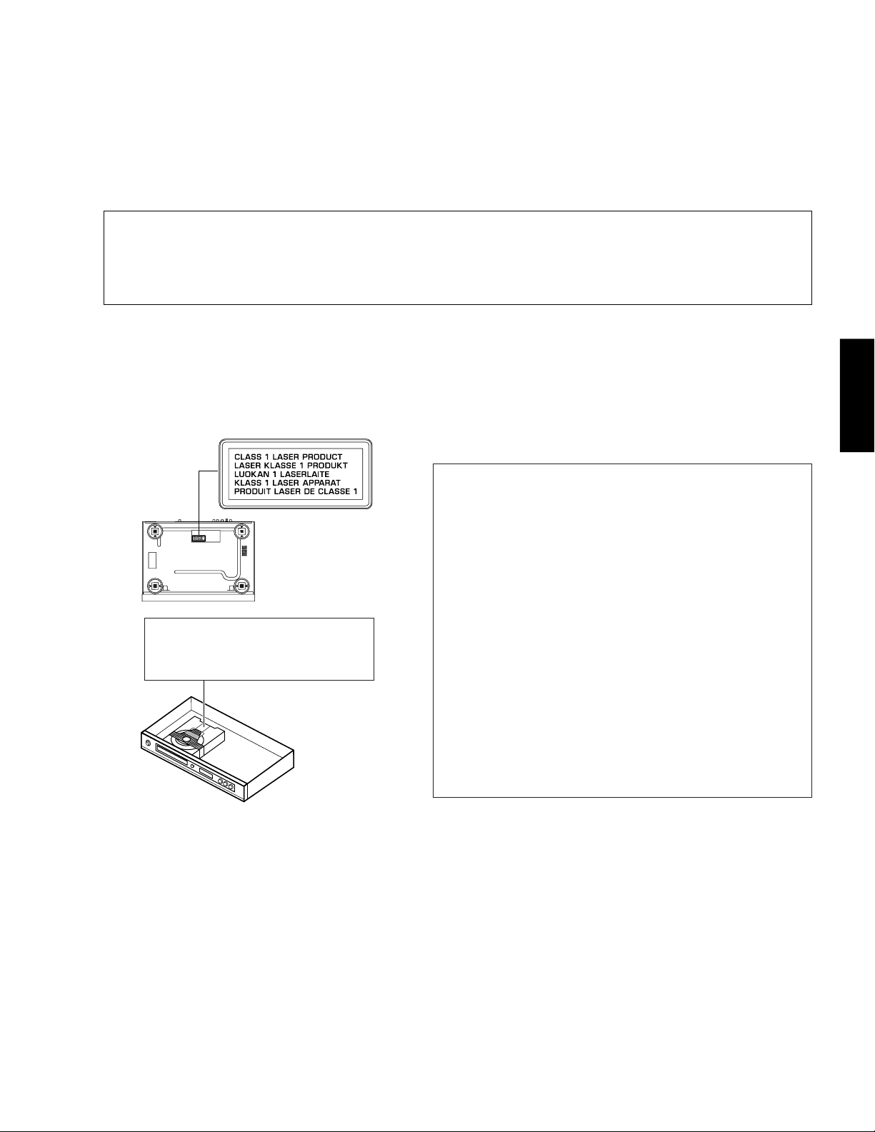
WARNING: Laser Safety
This product contains a laser beam component. This component may emit invisible, as well as visible radiation,
which may cause eye damage. To protect your eyes and skin from laser radiation, the following precautions must be
used during servicing of the unit.
1) When testing and/or repairing any component within the product, keep your eyes and skin more than 30 cm away from
the laser pick-up unit at all times. Do not stare at the laser beam at any time.
2) Do not attempt to readjust, disassemble or repair the laser pick-up, unless noted elsewhere in this manual.
3) CAUTION : Use of controls, adjustments or performance of procedures other than those specified herein may result in
hazardous radiation exposure.
Laser Emitting conditions:
1) When the Top Cover is removed, and the STANDBY/ON SW is turned to the "ON" position, the laser component will emit
a beam for several seconds to detect if a disc is present. During this time (5-10 sec.) the laser may radiate through the
lens of the laser pick-up unit. Do not attempt any servicing during this period!
If no disc is detected, the laser will stop emitting the beam. When a disc is loaded, you will not be exposed to any laser
emissions.
2) The laser power level can be adjusted with the VR on the pick-up PWB, however, this level has been set by the factory
prior to shipping from the factory. Do not adjust this laser level control unless instruction is provided elsewhere in this
manual. Adjustment of this control can increase the laser emission level from the device.
2
Page 3
DVD-S550/DV-S5750
Laser Diode Properties
Type: Semiconductor laser GaAlAs
Wave length: 650 nm (DVD)
780 nm (VCD/CD)
Output Power: 7 mW (DVD)
10 mW (VCD/CD)
Beam divergence: 60 degree
VARO! : AVATTAESSA JA SUOJALUKITUS OHITETTAESSA OLET ALTTIINA NÄKYMÄTTÖMÄLLE LASER-
SÄTEILYLLE. ÄLÄ KATSO SÄTEESEEN.
VARNING! : OSYNLIG LASERSTRÅLNING NÄR DENNA DEL ÄR ÖPPNAD OCH SPÄRREN ÄR URKOPPLAD.
BETRAKTA EJ STRÅLEN.
WARNING
The use of optical instruments with this product will increase eye hazard.
Repair handling should take place as much as possible with a disc loaded inside the player.
DVD-S550/DV-S5750
CAUTION VISIBLE AND INVISIBLE LASER RADIATION WHEN
OPEN. AVOID EXPOSURE TO BEAM.
ADVARSEL SYNLIG OG USYNLIG LASERSTRÅLING VED ÅBNING.
UNDGÅ UDSÆTTELSE FOR STRÅLING.
ADVARSEL SYNLIG OG USYNLIG LASERSTRÅLING NÅR DEKSEL
ÅPNES. UNNGÅ EKSPONERING FOR STRÅLEN.
VARNING SYNLIG OCH OSYNLIG LASERSTRÅLNING NÄR
DENNA DEL ÄR ÖPPNAD. BETRAKTA EJ STRÅLEN.
VARO! AVATTAESSA OLET ALTTIINA NÄKYVÄLLE JA
CAUTION:
DANGER:
INVISIBLE LASER RADIATION WHEN OPEN
DO NOT STARE INTO BEAM
INVISIBLE LASER RADIATION WHEN OPEN
AVOID DIRECT EXPOSURE TO THE BEAM
NÄKYMÄTTÖMÄLLE LASER SÄ TEILYLLE. ÄLÄ KATSO
SÄTEESEEN.
VORSICHT SICHTBARE UND UNSICHTBARE LASERSTRAHLUNG
WENN ABDECKUNG GEÖFFNET. NICHT DEM STRAHL
AUSSETSEN.
DANGER VISIBLE AND INVISIBLE LASER RADIATION WHEN
OPEN. AVOID DIRECT EXPOSURE TO BEAM.
ATTENTION RAYONNEMENT LASER VISIBLE ET INVISIBLE EN CAS
D'OUVERTURE. EXPOSITION DANGEREUSE AU
FAISCEAU
Warning for power supply
The primary side of the power supply carries live mains voltage when the player is connected to the mains even when
the player is switched off !
This primary area is not shielded so it is possible to touch copper tracks and/or components when servicing the player.
Service personnel have to take precautions to prevent touching this area or components in this area.
Note:
The screws on the DVD mechanism may never be touched, removed or re-adjusted.
Handle the DVD mechanism with care when the unit has to be exchanged!
The DVD mechanism is very sensitive for dropping or giving shocks.
3
Page 4
DVD-S550/DV-S5750
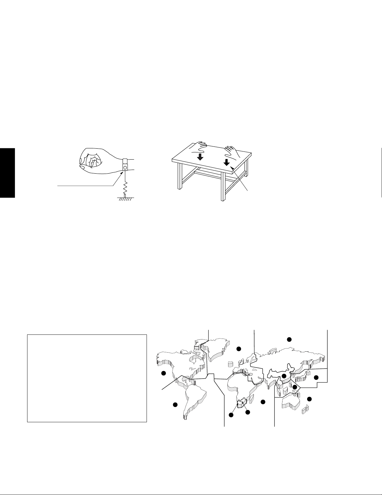
■ PREVENTION OF ELECTRO STATIC DISCHARGE
The laser diode in the DVD mechanism may be damaged due to static electricity from clothes or the human body. Use caution
to prevent electro static damage when servicing or handling the DVD-mechanism.
1. Grounding for electro static damage prevention
Some devices, such as the DVD player, use an optical pickup (laser diode) that will be damaged by static electricity in the
working environment. Only attempt service after ensuring that all grounding procedures have been completed.
1. Worktable grounding
Put a grounded conductive material (sheet) or iron sheet on the area where the optical pickup is placed.
2. Human body grounding
Use an anti-static wrist strap to discharge the static electricity from your body.
Anti-static wrist strap
DVD-S550/DV-S5750
1MΩ
Conductive material
(sheet) or steel sheet
2. Handling Precautions for DVD mechanism
1. Handle the DVD mechanism gently, as it is an extremely high-precision assembly.
2. The flexible cable lines may break if an excessive force is applied to it. Use caution when handling the cable.
3. The semi-fixed resistor for laser power adjustment should not be adjusted. Do not turn the resistor.
■ LOCALE MANAGEMENT INFORMATION
Locale Management Information : This DVD player is designed and manufactured to respond to the Locale
Management Information that is recorded on a DVD disc. If the Locale number described on the DVD disc does not
correspond to the Locale number of this DVD player, this DVD player cannot play this disc.
This product incorporates copyright protection technology that is protected by
method claims of certain U.S. patents and
other intellectual property rights owned by
Macrovision Corporation and other rights
owners. Use of this copyright protection
technology must be authorized by
Macrovision Corporation, and is intended
for home and other limited viewing uses
only unless otherwise authorized by
Macrovision Corporation. Reverse engineering or disassembly is prohibited.
2
1
4
2
5
5
5
6
3
2
4
4
Page 5
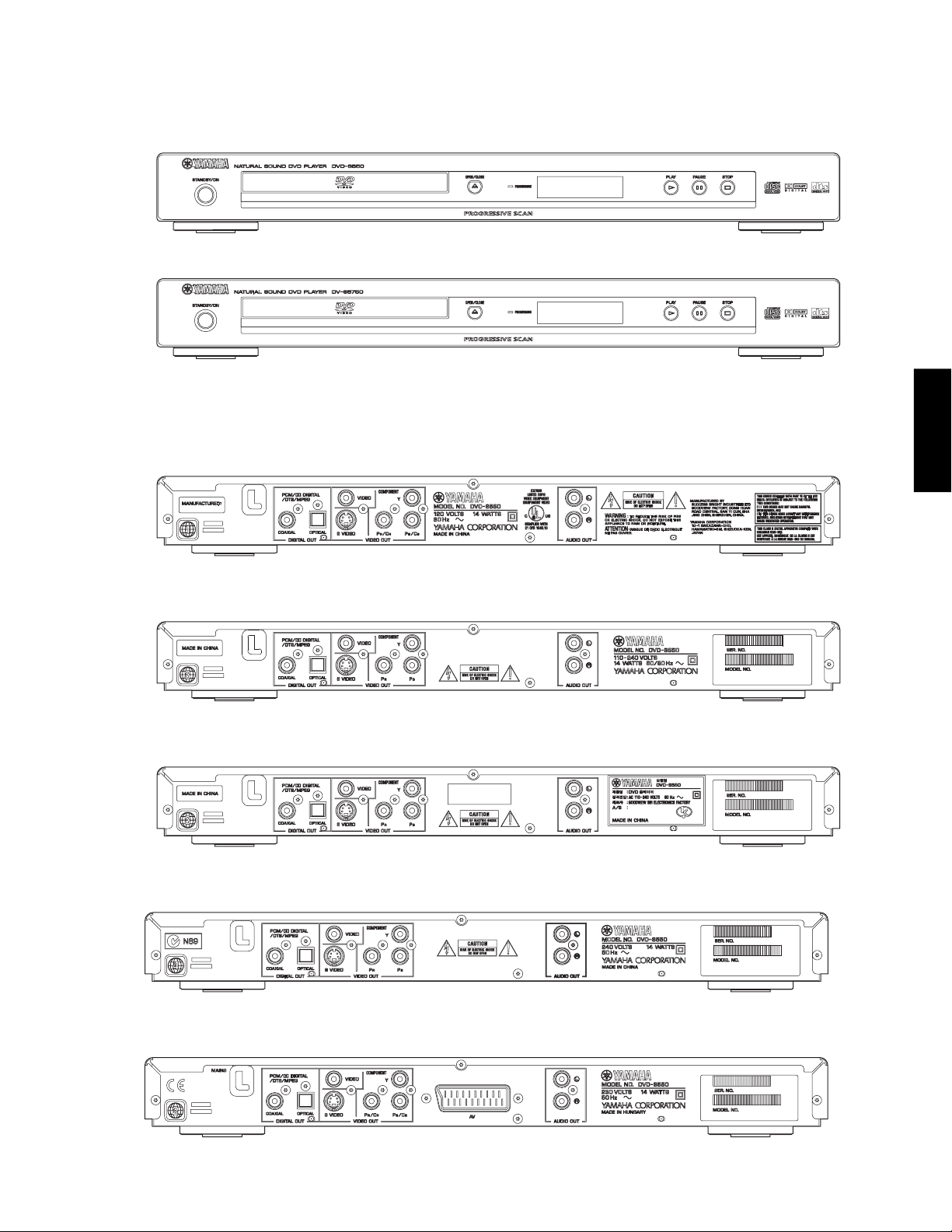
■ FRONT PANELS
▼ DVD-S550 (U, R, K, A, B, G, E, P models)
▼ DV-S5750 (U, A models)
■ REAR PANELS
▼ DVD-S550 (U model)
DVD-S550/DV-S5750
DVD-S550/DV-S5750
▼ DVD-S550 (R model)
▼ DVD-S550 (K model)
▼ DVD-S550 (A model)
▼ DVD-S550 (B, G, E models)
5
Page 6
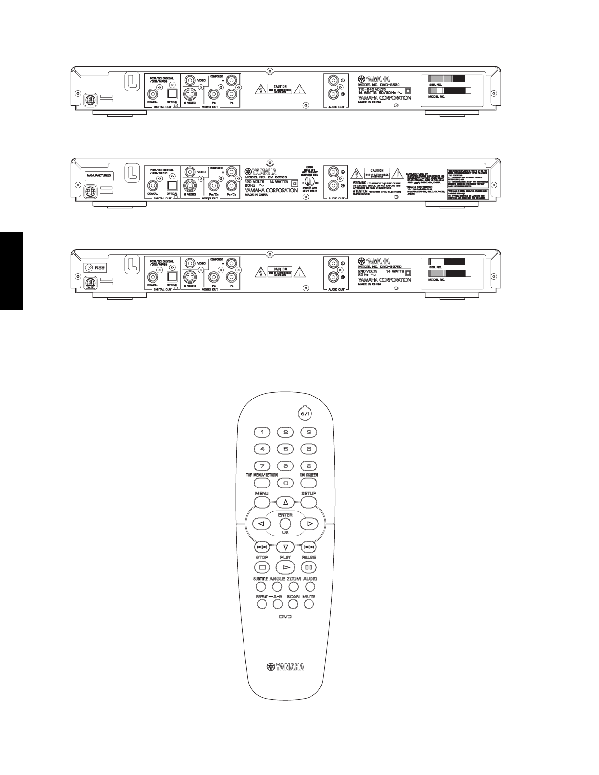
DVD-S550/DV-S5750
▼ DVD-S550 (P model)
▼ DV-S5750 (U model)
▼ DV-S5750 (A model)
DVD-S550/DV-S5750
■ REMOTE CONTROL PANEL
6
Page 7
■ SPECIFICATIONS
DVD-S550/DV-S5750
PLAYBACK SYSTEM
DVD Video
Video CD & SVCD
CD
PICTURE CD
CD-R, CD-RW
DVD+R, DVD+RW
DVD-R, DVD-RW
VIDEO PERFORMANCE
Video (CVBS) Output 1 Vpp into 75 ohm
S-Video Output Y: 1Vpp into 75 ohm
C: 0.3Vpp into 75 ohm
RGB (SCART) Output
Component Video Output Y: 1Vpp into 75 ohm
AUDIO FORMAT
Digital Mpeg/Dolby Compressed Digital
Digital/DTS
PCM 16, 20, 24 bits
MP3(ISO 9660) 24, 32, 56, 64, 96, 128, 256 kbps
WMA 32 kbps-192 kbps, mono, stereo
Analog Sound Stereo
AUDIO PERFORMANCE
DA Converter 24 bits
Signal-Noise (1kHz) 105 dB
Dynamic Range (1kHz) 100 dB
DVD fs 96 kHz 2 Hz - 44 kHz
SVCD fs 48 kHz 2 Hz - 22 kHz
CD/VCD fs 44.1 kHz 2 Hz - 20 kHz
Distortion and Noise (1kHz) 0.003%
0.7 Vpp into 75 ohm (B, G, E models)
Pb/Cb Pr/Cr: 0.7Vpp into 75 ohm
fs, 44.1, 48, 96 kHz
fs 16, 22.05, 24, 32, 44.1, 48 kHz
(U, R, K, A, P models)
fs 48 kHz 2 Hz - 22 kHz
fs 44.1 kHz 2 Hz - 20 kHz
GENERAL
Dimensions (W x H x D) 435 x 51 x 310 mm
(17-1/8" x 2" x 12-3/16")
Weight Approx. 2.6 Kg (5 lbs. 12 oz)
Finish [DVD-S550] Gold Color (R, K models)
Black Color (U, A, B, G, E, P models)
Titanium Color (U, G, E models)
Silver Color
[DV-S5750]
Power Supply AC120V, 60 Hz (U model)
Power Consumption Approx. 14W
Standby Power Consumption < 1W
ACCESSORIES
Audio/Video Cable (U, R, K, A, P models),
Black Color (U model)
Silver Color
AC240V, 50 Hz (A model)
AC110–240V, 50/60 Hz (R, K, P models)
AC230V, 50 Hz (B, G, E models)
Remote Control x 1, Battery x 2,
Audio Pin Cable (B, G, E models),
Video Cable (B, G, E models)
(B, G, E models)
(U, A models)
* Specifications subject to change without prior notice.
U ......... U.S.A model R ..........General model
K ......... Korean model A .......... Australian model
B ......... British model G .......... European model
E .......... South European model P .......... South American model
Manufactured under license from Dolby Laboratories.
“Dolby” and the double-D symbol are trademarks of Dolby Laboratories.
“DTS” and “DTS Digital Out” are trademarks of
Digital Theater Systems, Inc.
DVD-S550/DV-S5750
TV STANDARD (PAL/50Hz) (NTSC/60Hz)
Number of lines 625 525
Playback Multistandard (PAL/NTSC)
CONNECTIONS
SCART Euroconnector (B, G, E models)
Y Output Cinch (green)
Pb/Cb Output Cinch (blue)
Pr/Cr Output Cinch (red)
S-Video Output Mini DIN, 4 pins
Video Output Cinch
Audio Output (L+R) Cinch
Digital Output 1 coaxial, 1 optical
IEC60958 for CDDA / LPCM/
MPEG1
IEC61937 for MPEG 2,
Dolby Digital and DTS
DivX, DivX Certified, and associated logos are
trademarks of DivXNetworks, Inc and are used
under license.
This product incorporates copyright protection technology
that is protected by method claims of certain U.S. patents
and other intellectual property rights owned by Macrovision
Corporation and other rights owners. Use of this copyright
protection technology must be authorized by Macrovision
Corporation, and is intended for home and other limited
viewing uses only unless otherwise authorized by Macrovision
Corporation. Reverse engineering or disassembly is prohibited.
7
Page 8
DVD-S550/DV-S5750
■ SERVICE HINTS
● Repair Tips
1) DVD Module
The DVD Mechanism and Mono Board together as a set are called the DVD Module.
If a failure has occurred with any part of the DVD Module, be sure to replace the DVD Module as a whole.
Neither the DVD Mechanism nor Mono Board can be replaced independently.
2) Power Supply Unit
The power supply unit has to be replaced in case of failure.
3) PCB Ass’y
When the Front Board or AV Board has failed, replace the faulty board.
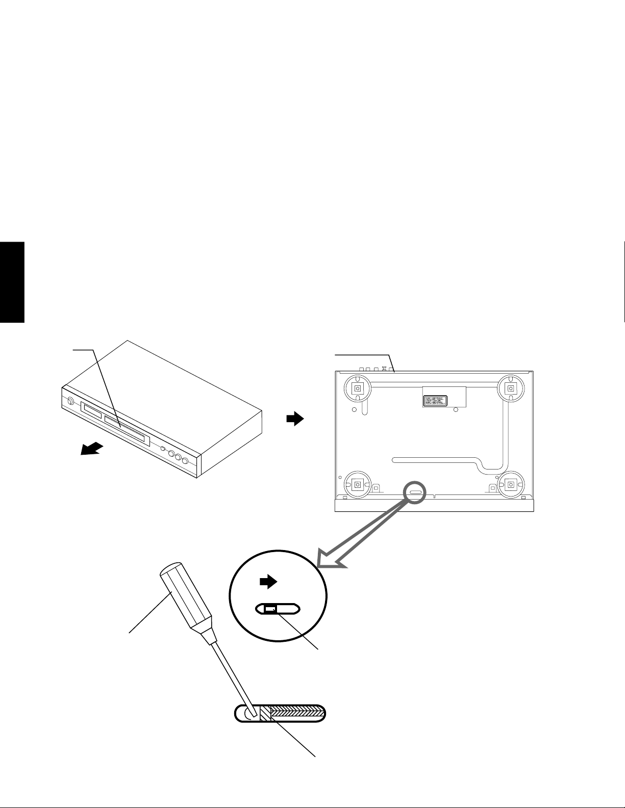
■ DISASSEMBLY PROCEDURES
HOW TO MANUALLY EJECT THE TRAY
a. Turn the player bottom up.
b. Move the slider in the direction indicated with a screw driver until the tray is ejected.
c. Gently pull the tray out.
DVD-S550/DV-S5750
Tr ay
Bottom Frame
Rear
a.
c.
Front
b.
Screw Driver
8
Slider
Slider
Page 9
See EXPLODED VIEW for item numbers.
Top Cover [240]
➔ Remove 5 screws [250].
(2 on side and 3 on rear
side)
➔ Lift cover from rearside to
remove.
DVD-S550/DV-S5750
Mounting
Dismounting
➔ Remove 3 cable connections.
Front Panel [101]
[1305][1105][1106]
➔ Open Tray (see HOW TO MANUALLY
EJECT THE TRAY).
➔ Unlock Tray cover and close tray.
➔ Unlock Front panel from frame by
releasing successively 4 snaps (2 on the
side and 2 on the bottom).
Front (1) Display board [1100(1)]
➔ Remove 4 screws [260]
(Board to Front panel).
➔ Dismount board.
Front (2) Standby board [1100(2)]
➔ Remove 1 screw [260].
(Board to Front panel).
➔ Dismount board.
➔ Remove cable connection. [1202]
➔ Remove 3 cable connections.
DVD Mechanism
[1101][1102][1103]
➔ Open tray (see HOW TO MANUALLY
EJECT THE TRAY).
➔ Unlock Tray cover and close tray.
➔ Remove 4 screws [256]
(DVD Mechanism to bottom).
➔ Lift DVD Mechanism up slightly and
move it backward to remove.
AV board [1002]
➔ Remove 4 cable connections.
[1112][1302][1303][1305]
➔ Remove 6 (U, R, K, A, P models) or
8 (B, G, E models) screws [260]
(Board to rear panel).
➔ Release 2 spacers.
(Board to bottom frame).
➔ Dismount board.
DVD-S550/DV-S5750
➔ Remove 7 cable connections.
MONO board
[1101][1102][1103][1104][1105]
[1106][1301]
➔ Remove 4 screws [255] (Board to
bottom frame).
➔ Dismount board.
➔ Remove 2 cable connections.
[CN101][CN202]
➔ Remove 2 screws [255].
(Board to bottom frame)
➔ Release 2 spacers.
(Board to bottom frame).
➔ Dismount board.
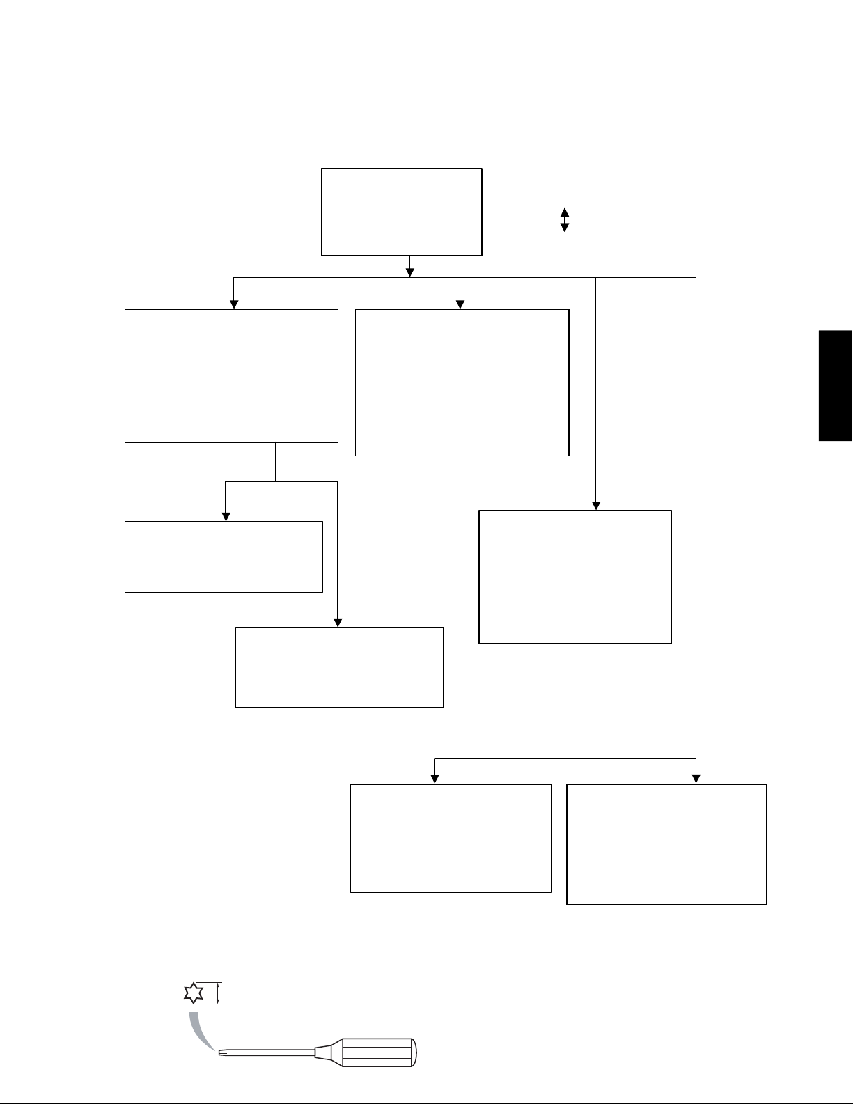
When disassembling,use the special screw driver with such tip shape as shown in figure.
T10
2.7 mm
Power supply unit [1600]
9
Page 10

DVD-S550/DV-S5750
■ MAINTENANCE FLOW CHART
Start
Power on
at all pins of connector (Ref 1303)
at +8V and +1V8 of power part
AV Board
DVD-S550/DV-S5750
Are voltages
in AV Board normal ?
Ye s
Are voltages
normal ?
Ye s
Is voltage
at +5V VL of power part
normal ?
Ye s
Are voltages
at pins of connector (Ref 1104)
in Mono Board
normal ?
No
No
No
No
1. Check Cable
2. Replace power supply unit if AV Board is not shorted,
otherwise find out first where the short is.
Check L7808 (Ref 7301) and LD1117 (Ref 7303) and peripheral
circuit.
Check S12302 (Ref 7306) and peripheral circuit.
1. Check Cable
2. Replace AV Board if Mono Board is not shorted, otherwise
find out first where the short is.
10
MONO Board
Ye s
Is voltage
at +3V3 of power part
normal ?
Ye s
A
No
Check LD1117 (Ref 7101) and peripheral circuit.
Page 11

DVD-S550/DV-S5750
A
MONO Board
AV Board
Is logo displayed
on TV screen?
Ye s
No
Is
Main Clock
normal ?
Ye s
Is
reset signal
normal ?
Ye s
Is signal
on FLASH (Ref 7303)
normal ?
Ye s
Is signal
on DRAM (Ref 7302)
normal ?
Ye s
Is image signal
at connector (Ref 1301) in
Mono Board normal?
Ye s
Is image signal
at output terminal in AV
Board normal?
Ye s
Check 74HCU04 (Ref 7103) and
No
peripheral circuit.
No
Check NCP303 (Ref 7102) and
peripheral circuit.
No
Check peripheral circuit of FLASH (Ref 7303)
No
Check peripheral circuit of DRAM (Ref 7302)
Check MT1389 (Ref 7112) and
No
peripheral circuit.
No
Check video filter circuit and
amplification circuit in AV board.
DVD-S550/DV-S5750
Does the tray
automatically close when
MONO Board
it is open?
Ye s
B
Check TV connection cable.
No
Are signals TROUT
(Pin 48 of MT1389) and TRIN
(Pin 49 of MT1389)
correct ?
Are signals
TRCLOSE & TROPEN
correct ?
Are signals
LOAD+ & LOAD-
correct ?
Check the circuits connecting
to the DVD mechanism
Ye s
Ye s
Ye s
No
No
No
Check the position-switch on
the DVD mechanism
Check the circuit between
MT1389 and MM1646
Check MM1646 and peripheral
circuit
Board Ref Name
MONO 7111 MM1646
MONO 7112 MT1389
11
Page 12

DVD-S550/DV-S5750
B
automatically move to inside
when it is outside ?
DVD-S550/DV-S5750
Optical Pick Up move to find
Does sled
Ye s
Does
a disc ?
No
No
STBY (Pin 1 of MM1646)
(Pin 5 of MM1646) more
(Pin 11 of MM1646) & SL-
Check the copper trace or cable
connected to the DVD
mechanism
Is signal
high level ?
Is signal FMO
than 1.4V ?
Are signals SL+
(Pin 12 of MM1646)
correct ?
Has FOO
(Pin 3 of MM1646)
any signal?
Ye s
Ye s
Ye s
No
No
No
No
Check the STBY circuit
Check the FMO circuit
Check MM1646 and
peripheral circuit
1. Check the signal from
MT1389 to MM1646
2. Maybe MM1389 is not
working
MONO Board
disc, is Laser on OK ?
Ye s
When read
Ye s
Is a disc loaded ?
Ye s
No
Are signals F+
(Pin 14 of MM1646) & F-
(Pin 13 of MM1646)
correct ?
Check the cable and circuit
between the DVD mechanism
and MM1646
No
Laser off
Are signals LDO1
(Pin 23 of MT1389) & LDO2
(Pin 22 of MT1389)
correct ?
Is voltage
of +L_V33 OK ?
Ye s
Ye s
Ye s
Ye s
No
No
No
Check the peripheral circuit of
MM1646
Check peripheral circuit of
MT1389
Check peripheral circuit of
two transistors (Ref 7106
& 7107)
Check peripheral circuit of
two transistors (Ref 7106
& 7107)
Check connection circuit of
the DVD mechanism
Optical Pick Up may be
damaged
12
C
Board Ref Name
MONO 7111 MM1646
MONO 7112 MT1389
Page 13

DVD-S550/DV-S5750
C
MONO Board
Is Focus on OK ?
Ye s
Is Spindle on OK ?
Ye s
No
No
Is any signal
on pins A B C D E F of
MT1389 turned
ON ?
Ye s
Check MT1389 and its
peripheral circuit.
Is DMO
(pin 37 of MT1389)
normal ?
Ye s
Are signals SP+
(Pin 17 of MM1646) & SP-
(Pin 18 of MM1646)
correct ?
Ye s
Check connection between
spindle driver and MM1646
No
No
No
Check circuit between Optical
Pick Up and MT1389
Check MT1389 and its
peripheral circuit.
Check MM1646 and its
peripheral circuit
DVD-S550/DV-S5750
Is Track on OK ?
Ye s
Is disk READY ?
Ye s
D
No
No
Is signal TRO
(pin 41 of MT1389)
normal ?
Ye s
Are signals T+
(Pin 16 of MM1646) & T-
(Pin 15 of MM1646)
correct ?
Ye s
Check connection between
Optical Pick Up and MM1646
Check cable and circuit
between DVD mechanism and
MT1389
No
No
Check connection between
MT1389 (pin 41) and MM1646
(pin 24)
Check MM1646 and its
peripheral circuit.
Board Ref Name
MONO 7111 MM1646
MONO 7112 MT1389
13
Page 14

DVD-S550/DV-S5750
D
Is audio signal normal ?
AV Board
Are TSOP2236,
DVD-S550/DV-S5750
FL display and Key function
DISPLAY Board
OK ?
END
Ye s
Ye s
No
No
Does AKM4382A
receive correct data ?
Ye s
Is output signal
correct ?
Ye s
Check circuit of filter,
amplifier, and mute etc.
Do TSOP2236
and uPD16312 communicate
with MT1389 ?
Ye s
Check Remote Control
Check KEY matrix
Check connection of FL display
No
No
Check connection between
MT1389 and AKM4382A
Check AKM4382A and its
periperal circuit
Check connection between
No
MT1389 and uPD16312 and
their periperal circuit
Board Ref Name
DISPLAY 7100 uPD16312
DISPLAY 7102 TSOP2236
MONO 7111 MM1646
MONO 7112 MT1389
AV 7234 AK4382A
14
Page 15

ABCDEFGH
■ BLOCK DIAGRAM
1
DVD-S550/DV-S5750
AUDIO OUT
L / R
1113
72347233 7105
2CH
AUDIO
2
DAC
AV (SCART)
(B, G, E models only)
ADG733BRU
Y
1109,
1110
7108, 7109
VIDEO OUT DIGITAL OUT
PB/CBPR/C
S VIDEO VIDEO
R
1103
OPTICAL COAXIAL
13071300 7311
+/-12V, +5v, +3V, -24V
AV BOARD
1301 1112 1305 1303
1104 1301
3
7111
7112
7301
8k byte
EEPROM
7302
CN202
DVD MECHANISM
ASA + DV34
11021103 1101
MTK1389
MOTOR
DRIVER
7303
64M bit
DRAM
8M bit
FLASH
POWER SUPPLY UNIT
4
MONO BOARD
1106 1105
1202
STANDBY / ON
1100
5
1201
FTD DISPLAY
GRID
SEGMENT
FRONT (2) STANDBY BOARD
DATA/CLK/STB IR
7100
TACT SWITCH
µPROCESSOR
µPC16312
FRONT (1) DISPLAY BOARD
11011102
7102
IR
CN101
6
15
Page 16

ABCDEFGH
DVD-S550/DV-S5750
■ WIRING DIAGRAM
1
26
1100 (2)
1
FRONT (2)
STANDBY BOARD
DVD MECHANISM
1
VSTB
2
1100 (1)
FRONT (1)
DISPLAY BOARD
+5VL
+12VL
GND
+5VSTBY
1
-24V
VSDA
VSCK
GND
46kHz
IR
io Power ON
NC
LED5
1300
(ASA)
1
1
5V
-24V
GND
+12VL
1200
+5V_EVER
For Line Out
To control DAC
GND
TU_SD
S1-L3-1
S0-L3-0
AV_MUTE
GND
GND
GND
CVBS
GND
G_Y
GND
B_Cb
GND
R_Cr
GND
PCM_LRCK
PCM_LTRT
GND
PCM_MCLK
PCM_SCLK
GND
SPDIF_OUT
GND
PCM_MIC_IN
GND
MIC_DET
GND
GND
+1V8_SENSE
+1V8
+1V8
+5VL
+5VL
+5VL
GND
GND
STBY
RDS_DAT
VSCK
VSDA
GND
L2
Y
C
1
+8V
3
1
1600
PSU
1
+3V3
+3V3
GND
+12V
+12STBY
GND
+5V
GND
-12V
GND
-24V
STDBY CONTROL
CN101
AV BOARD
4
VSTB
VSDA
VSCK
GND
TU_SD
L2
S1-L3-1
S0-L3-0
AV_MUTE
GND
Y
GND
C
GND
CVBS
GND
G_Y
GND
B_Cb
GND
R_Cr
GND
PCM_LRCK
PCM_LTRT
GND
PCM_MCLK
PCM_SCLK
GND
SPDIF_OUT
GND
PCM_MIC_IN
GND
MIC_DET
GND
GND
+1V8_SENSE
+1V8
+1V8
+5VL
+5VL
+5VL
GND
+8V
GND
STBY
RDS_DAT
VSCK
VSDA
GND
PCS
GND_D
PCM_LRCK
STBY
VOL_A
VOL_B
+5D
GND
STBY
STB_SW
1300
MONO BOARD
SL+
SL-
SP-
SP+
GND
LIMIT
LOAD-
LOAD+
TROUT
GND
TRIN
GND-LD
DVD_LD
HFM
CD_LD
VD_DVD
VD_CD
VCC
GND-PD
CD/DVD
+3V3
RxD
TxD
GND
1
NC
MD
NC
E
Vref
F
B
A
RF
C
d
TT+
F+
F-
26
5
Interface connection
Audio Signal Dig Aud Sig Video Signal
COAXIAL COMPONENT
L/R OUT OPTICAL S-Video
Y, P
R/CR
CVBS
SCART
, PB/C
B
GND
+3V3
+D
-D
16
6
Page 17

■ PRINTED CIRCUIT BOARD
FOR INFORMATION ONLY (NO SERVICE PARTS WILL BE AVAILABLE)
DVD-S550/DV-S5750
The first digit of a component indicates the component type.
1xxx : Connector 3xxx : Resistor 5xxx : Coil 7xxx : IC, Transistor, FET
2xxx : Capacitor 4xxx : SMD jumper 6xxx : Diode 9xxx : Wire jumper
FRONT(2) STANDBY BOARD 1202
Page 19
FRONT(1) DISPLAY BOARD 1102
MONO Board-Top View
1
B
Page 18
AV BOARD 1301
1
A
Page 20
6
B
MONO Board-Bottom View
4
B
Page 20
AV BOARD 1112
DVD MECHANISM DVD MECHANISM
17
Page 18

DVD-S550/DV-S5750
■ PRINTED CIRCUIT BOARD
FOR INFORMATION ONLY (NO SERVICE PARTS WILL BE AVAILABLE)
The first digit of a component indicates the component type.
1xxx : Connector 3xxx : Resistor 5xxx : Coil 7xxx : IC, Transistor, FET
2xxx : Capacitor 4xxx : SMD jumper 6xxx : Diode 9xxx : Wire jumper
FRONT (1) Display Board-Top View
MONO BOARD 1105
Page 17
1
A
AV BOARD 1305
Page 20
1
A
FRONT (1) Display Board-Bottom View
18
Page 19

■ PRINTED CIRCUIT BOARD
FOR INFORMATION ONLY (NO SERVICE PARTS WILL BE AVAILABLE)
DVD-S550/DV-S5750
The first digit of a component indicates the component type.
1xxx : Connector 3xxx : Resistor 5xxx : Coil 7xxx : IC, Transistor, FET
2xxx : Capacitor 4xxx : SMD jumper 6xxx : Diode 9xxx : Wire jumper
FRONT (2) Standby Board-Top View
FRONT (2) Standby Board-Bottom View
MONO BOARD 1106
Page 17
1
A
19
Page 20

DVD-S550/DV-S5750
■ PRINTED CIRCUIT BOARD
FOR INFORMATION ONLY (NO SERVICE PARTS WILL BE AVAILABLE)
AV Board-Top View
The first digit of a component indicates the component type.
1xxx : Connector 3xxx : Resistor 5xxx : Coil 7xxx : IC, Transistor, FET
2xxx : Capacitor 4xxx : SMD jumper 6xxx : Diode 9xxx : Wire jumper
POWER SUPPLY UNIT CN202
FRONT(1) DISPLAY BOARD 1101
Page 18
MONO BOARD 1301
U, R, K, A, P models only
11
A
1
Page 17
D
U, R, K, A, P
models only
MONO BOARD 1104
U, R, K, A, P
models only
Page 17
2
A
20
COAXIAL
U, R, K, A, P models only
OPTICAL AV(SCART) L/RVIDEO
DIGITAL OUT AUDIO OUT
S-VIDEO
PR/C
R
VIDEO OUT
Y
PB/C
B
B, G, E models only
Page 21

■ PRINTED CIRCUIT BOARD
FOR INFORMATION ONLY (NO SERVICE PARTS WILL BE AVAILABLE) AV Board-Bottom View
DVD-S550/DV-S5750
The first digit of a component indicates the component type.
1xxx : Connector 3xxx : Resistor 5xxx : Coil 7xxx : IC, Transistor, FET
2xxx : Capacitor 4xxx : SMD jumper 6xxx : Diode 9xxx : Wire jumper
21
Page 22

DVD-S550/DV-S5750
■ SCHEMATIC DIAGRAM
FOR INFORMATION ONLY (NO SERVICE PARTS WILL BE AVAILABLE)
The first digit of a component indicates the component type.
1xxx : Connector 3xxx : Resistor 5xxx : Coil 7xxx : IC, Transistor, FET
2xxx : Capacitor 4xxx : SMD jumper 6xxx : Diode 9xxx : Wire jumper
MONO BOARD 1/2
D5
+
5101
+5VL
+3V3
+5D
SFV24R-1ST
1101
1
2
3
4
5
6
7
8
9
10
11
12
13
14
15
16
17
18
TO DVD MECHANISM
19
20
21
22
23
24
B6B-PH-K
6
5
4
3
2
1
1102
TO DVD MECHANISMTO DVD MECHANISM
1103
1
2
3
4
5
B5B-PH-K
1012u022
2012n001
A33VD+
5105
1
2112n00
112n001
1
5V_F
R
+
5109
8312
u
022
u022
391
2
+RF_V5
2526
3V3+
7101
LD1117DT33
32
COM
5102
OUTIN
3012u022
1
5106
+3V3
3112n001
7112n001
M5+
5111
+5D
9312n001
5126
3146
390R
E
2197 100n
2198
F
V20
B_
A_
D_
2412n001
1412u74
n0014912
100n
K0
7109
0
BSH103
10513
3152 10K
VO2
LIMIT
3171 1R0
3172 1R0
77
3
7
1
13
3K01
K
033
+PO
4713K03
3
-PO
LOAD-
LOAD+
TROUT
TRIN
3176 10K
+3V3
+3V3
10K3175
4012u74
B3
3
VD+
8
11
2
n001
+8V
10u 5125
3V3+
+3V3
9112n00
1
5112
IOAC_
MM1646XH
6
14
13
12
11
17
18
15
16
19
20
0
212
n001
7111
VO2
OUT1p
OUT1n
OUT2p
OUT2n
OUT3p
OUT3n
OUT4p
OUT4n
OUTLp
OUTLn
5412u74
7108
BSH103
5103
1212n001
M8+
3148 10R
M8
+
9
C
C
VRWP
5
012u0
2
2
2212n001
3212n001
6412n001
7107
2SB1132
9
K
4
0
13
0
1
3151
7110
BC817-25W
8
DNG_SH
92
03
33V_S+
+3V3
6012n001
+3V3
3
3
V
_L+
6912
u74
10K
Φ
D
NGRWP
01
12
+RF_V5
M5+
22
C
CV
ERP
VINLOp
DNG
VINLOn
E
RP
52
5104
5107
8P2V
0812u74
512410u
M
8+
VBIAS
VIN1
VIN2p
VIN2n
VIN3
VIN4
33V_L+
7012u022
33V_V+
6
212u01
02V
2
1812
8
12u74
n
001
7106
2SB1132
7
1
PS
2
28
SB
3
4
5
23
24
27
26
* Components having special characteristics are marked Z and
must be replaced with parts having specifications equal to those
originally installed.
* Schematic diagram is subject to change without notice.
+3V3
XTALI
8
0
1
2
n
0
0
1
+1V8
7
212n001
4812
3
8
1
2
n001
u74
3147 10R
n0
K011
01
1122
6
13
2
33
1
2
n0
01
+3V3
V1P4
FOO
VO2
V1P4
FMO
DMO
V1P4
V1P4
TRO
TRCLOSE
TROPEN
3
5712
p01
4312
n001
ESNES_8V1+
721
4
OX
5312
n001
2191 120p
4116
4118
4119
V2P8
V20
V1P4
2202 100n
8V1+
417
11
74HCU04PW
74HCU04PW
6
312n001
E
F
5123
2207100n
2208100n
4
NM
0
11
F
1
22R3197
4
22R3198
7103-2
7103-1
1u02186
1u02187
2188
1u0
1u02189
2190 1u0
F141
4115
4117
F155
F156
DMO
FMO
TROPEN
TRO
FOO
10R3156
3157 10R
4122
ADIN
TROUT
TRIN
STBY
TRCLOSE
+V18
)
12:
A(2)
0(A
A(3)
A(4)
A(5)
A(6)
A(7)
A(8)
A(18)
A(19)
1n52209
ES
NES_8V1
+
2
4
5
3
TO 1301 OF AV BOARD
8V
1
+
XTALI
2522p01
1
2
3
4
5
6
7
8
9
10
11
12
13
14
15
16
17
18
19
20
21
22
23
24
25
26
27
28
29
30
31
32
33
34
35
36
37
38
39
40
41
42
43
44
45
46
47
48
49
50
51
52
53
54
55
56
57
58
59
60
61
62
63
64
6
PCM_MIC_IN
3522
p01
+S_V33
9115
AGND
DVDA
DVDB
DVDC
DVDD
DVDRFIP
DVDRFIN
MA
MB
MC
MD
SA
SB
SC
SD
CDFON
CDFOP
TNI
TPI
MDI1
MDI2
LDO2
LDO1
SVDD3
CSO
RFLVL
SGND
V2REFO
V20
VREFO
FEO
TEO
TEZISLV
OP_OUT
OP_INN
OP_INP
DMO
FMO
TROPENPWM
PWMOUT1
TRO
FOO
USB_VSS
USBP
USBM
USB_VDD3
FG
TDI
TMS
TCK
TDO
DVDD18_1
IOA2
IOA3
IOA4
IOA5
IOA6
IOA7
HIGHA0
IOA18
IOA19
DVSS_1
APLLCAP
APLLVSS
6112n001
4112u22
LV5+
789
Page 27
V1P4
n001271
n001371
2
2
K514413
652
552
452
3
FERI
CGFR
D
D
VA
3DDVLLPA
#RW
61A
OI
56
66
76
3V
RW
3
P
+
)
61(
A
V8+
01
22p2165
3143
100K
n001
n0011712
n338612
9
612
942
842
052
152
352
252
PSO
PQ
PLPTRC
N
DNGFR
NQEC
S
EC
O
1_3DD
7AHG
6AHG
4
3AHGIH
5AHGIH
A
H
G
V
I
I
I
H
H
H
D
96
0
86
17
27
37
7
A33
V
)2
)
)31(A
)11(A
D+
5
1(A)41(
1(
A
A
TAD_SDR
YBTS
1121314151
7
B
+S_V33
n0014
8115
6
1
2
0n16612
n0017612
64
54
742
2
2
CZFRH
C
APRFR
100n2163
0
n1
261
100n2161
2
n0
01
851
711
2
5
0
n
u
74
1951
7
51
2
2
242
732
832
0
4
932
142
3
4
4
4
2
2
2
3DDVFR
3
POFPL
SSVCDA
PFERV_S
CDPRF
R
NIFPL
N
M
D
FE
CV
DVC
RV_S
_S
DA
2153 100n
3142
680K
8
+S_V33+S_V33
n001
61
551
1
2
5
n07
44
n
74
512
6
51
2
332
5
4
632
3
3
2
2
3DDVLLP
PIFPL
N
O
FPL
1V
+
u0
n001
1
941
511
251
2
5
2
ILATX
OX
922
522
722
622
822
23
0
132
32
2
ILA
81DNGFR
8
PLXECADI
SSVLLP
NF
OLATX
OF
1D
T
T
T
IJ
IJ
D
X
VF
R
B_Cb
5913
0322
N
I
_
C
IM_
R
p
M
0
74
CP
5
1
1
R22
413
T
ef
R
T
sC_MC
L
T
U
L_M
C_MC
O
8
_PS
1V+
C
P
P
P
3
91
0
1
2
422
22
2
2
2
2
2
2
2
6_
4ATADSA
31_SSVD
2
3ATADSA
FIDPS
A
ATADSA
TA
8
1DDVD
D_
C
M
G_Y
1u8
49
13
R
051
1u8
5135
47p
2229
150R
3185
6
9
1
3
R05
1
KLCM_MC
K
KC
s
LCS
RsL
R
R
L_M
L_
_
_
M
MCP
M
CP
C
C
P
P
P
6
4
512
7
3
1
12
1
12
2812
2
2
1
0
K
KCBA
K
1_S
L
ATADSA
AT
C
CA
RLA
A
SV
DS
D
A
5134
8
22
47p
2227
2
p
150R
3184
74
R_Cr
1u8
5136
23
22
47p
2231
p7
150R
3186
4
PCM_MIC_IN
_
V
KLC_S
T
KL
KC
A
B33
_
TAD
KC
ETUM
C
RLPS
MPS
B
VD+
D
P
PS
R
S
1
7
0
60
9
2
802
1
0
12
1
02
2
2
2
2
01_3DDVD
7VUY
K
ATADPS
K
KLCMPS
NYSH
C
CB
RLP
PS
S
33V
B33V
_
D+
V+
041
R2
2
3
2
502
0
102
9
402
3
9
0
0
02
1
2
2
5V
6VUY
4
9_3DDVD
ASSVCA
NYSV
V
UY
UY
D
5133
2225
3183
5131
2221
3181
33V
_
V+
7918
6
3
4
591
9
91
9
91
1
1
3V
2VUY
1VUY
BDDVCAD
BSSVCA
A
CS
DDV
UY
S
VCA
CAD
D
D
DACVDDC
DVDD3_8
DVSS_11
DVDD18_5
DVDD3_7
DVSS_10
7112
MT1389
DVSS_9
DVDD3_6
DVDD18_4
DVSS_8
DVSS_7
DVDD3_5
DVSS_6
2
_
2A
1A
#S
02
H
H
1
A
A
C
G
GIH
I
OI
OI
OI
H
97
67
77
47
57
87
ECP
)
)01(A
)9
)
0
2(
1(
(
A
A
A
KCSV
ADSV
2_SSVD
3D
#EOOI
D
0DA281DA382DA
V
D
08
18
)0
)1
A3
D
(
(D
R
3
D
P
VD+
A
A
AD(0:7)
1
013
K0
1
1
2A
6DA
3DA
4DA785DA
ELA
OI
09
19
68
98
48
58
88
)6
)
)
)
)
2
3(D
(
DA
A
D5+
p
001
14
22
)
7
4(D
5
(
(
(
DA
DA
DA
A
)1
2(
A
A
BTS
DSV
V
p001
p00
1
3
242
422
2
2
_
81
3
_S
2_1PU
4_
3_1PU
5_1PU
#R
#DRU
D
0A
SVD
DVD
7DA
71A
O
I
39
49
29
)
0(
A
)71(A
KC
R
L_
KCSV
MC
P
6013
20
1
30K
2K1
1
1
WU
P
U
0
201
101
59
79
99
0
69
89
1
70
0
8013
901
113
1
3
3
R0
R
0K1
R
00
01
01
1
81
K
A
BT
C
DSV
V+
S
SV
V
Y
BL
ALOV
6
B
T
C
OV
S
R
3
4013
p
p0016422
p0
p0018
0
00
130
01
154
7422
0
422
22
K1
K
1
3_3
6
7_1PU
_1PU
401
30
1
11
2113
13
R01
R
33
CA
C
A
D
D_A
_L
C
D
S
S
#TSRP
1_3PU
4_3PU
5_3PU
0_3PU
501
601
701
31
1
3
Dx
R33
DxT
R
_ETUM_VA
_W
S_
BTS
3V3
+
0MQD
#0
0
D
SQD
DVD
901
801
41
13
0K
1
A
33
V
D+
7DR
ECI
T
N
R
I
I
6
011
111
311
411
511
211
1
1
60
14
)
7(
0M
6
A
Q
C
OI
D
R
Q
D
3_81
4_SSVD
5_SSVD
5
4
6
D
DR
DR
R
021
121
811
91
711
1
)5
)4(
)6
(
(Q
Q
QD
D
D
4_3DDVD
D
51DR
41DR
2DR
0DR
3
1DR
DVD
D
R
321
421
521
721
821
221
621
)41
)51(
)2(QD)1
)0(
)3
B
3
81V+
(Q
(QD
(Q
3V
Q
Q
D
D
D
D
D+
3V3
+
511
37
NCP303LSN30
K
4
1
OUTP
RESET
3
1105
123
61
TO 1102 OF FRONT (1) DISPLAY BOARD
456
09FMN-BMT-A-TFT
Page 24
8
9
7
E
1
234
1108
B4B-PH-K
1
CVBS
1u8
6
3913
222
47p
R0
51
D
D
1u8
47p
150R
Y
191
3
R
0
51
D
D
NB
560R
100n
22R
22R
22R
22R
22R
22R
22R
22R
22R
22R
22R
22R
22R
22R
22R
22R
330R
22R
MA(4)
MA(5)
MA(6)
MA(7)
MA(8)
MA(9)
MA(11)
DCKE
DCLK
+DV33B
F126
+V18
MA(3)
MA(2)
MA(1)
MA(0)
MA(10)
BA1
BA0
CS
+DV33B
RAS
CAS
WE
DQM1
LIMIT
DQ(8)
DQ(9)
DQ(10)
DQ(11)
DQ(12)
DQ(13)
_W
S
Y
_
BTS
BT
S
1
3
2
04FMN-BTRK-A
C
422
2
p74
D
+V_V33
MIC_DET
SP_RST
S0_L3_0
S1_L3_1
L2
TU_SD
+DV33B
TU_CE
TU_DI
TU_DO_ST
TU_CLK
ERR
AMP_ON
PW_DN_
+V18
FREQ_HOP
VOLA
RDS_DAT
STBY
VOLB
+DV33B
)
11
:0(AM
)
5
1
:
0(QD
D5
D
5+
+
71
13
K
01
1106
4
D
Page 24
p74
150R
D
5132
2223
3182
1u8
222
47p
2
p
150R
74
D
NB : 3139 = 1k8 for high Z mode
192
F128
YUV0
191
3139
FS
190
2151
VREF
189
3138
188
RD16
3137
187
RD17
3136
186
RD18
3135
185
RD19
3134
184
RD20
3133
183
RD21
182
3132
181
RD22
3131
180
RD23
3130
179
DQM2
3129
178
DQM3
3128
177
RD24
3127
176
RD25
175
174
RD26
3126
173
3124
172
RD27
3123
171
RD28
3122
170
RD29
3121
169
RD30
3120
168
RD31
167
166
RA4
165
RA5
164
RA6
163
162
RA7
161
160
RA8
159
RA9
158
RA11
157
CKE
156
RCLK
155
154
RCLKB
F125
153
RVREF
152
151
RA3
150
RA2
149
RA1
148
147
RA0
146
RA10
145
BA1
144
143
BA0
142
RCS#
141
140
RAS#
139
CAS#
138
RWE#
137
DQM1
136
DQS1
135
RD8
134
133
RD9
132
RD10
131
RD11
130
RD12
129
RD13
7102
2
INP
+5D
4
NC
CDGND
0
5
512n
00
1
TO 1202 OF FRONT (2) STANDBY BOARD
2913
R05
1
D
1
B
4
1
1
7
3145
100K
4
5130
712
27M
p01
81V
+
2312n001
1312n001
5108
5151
100n2251
4131
u022 0312
4P1V
5
8
1
2
n0
01
+S_V33
ADIN
591
2
u
74
33V
_
L+
C_
B_
A_
D_
5122
100n 2201
100n2203
2n22204
3153 680K
OP-
OP+
3154 680K
V1P4
2210 2n2
A
-KRTB
1
7
2
011
-
3
NMF40
4
2212
STBY
V1P4
470p
27K3162
3164 15K
2214 100n
2213 150n
V1P4
3163 56K
8K23165
100n2215
470p2216
3166 22K
10K
3168
3167 10K
22
Page 23

■ SCHEMATIC DIAGRAM
FOR INFORMATION ONLY (NO SERVICE PARTS WILL BE AVAILABLE)
1 2 3 4 5 6 7 8 9 101112
MONO BOARD 2/2
A
G
7301
M24C16-RDW6
1
2
3
B
C
MA(0:11)
MA(0)
MA(1)
MA(2)
D
E
MA(3)
MA(4)
MA(5)
MA(6)
MA(7)
MA(8)
MA(9)
MA(10)
MA(11)
F
1
23
0
24
1
25
2
26
3
29
4
30
5
A
31
6
32
7
33
8
34
9
22
10
35
11
20
0
21
BA
1
38
CLK
37
CKE
19
CS
18
RAS
17
CAS
16
WE
821445
8
F
(2Kx8)
EEPROM
0
ADR
1
2SDA
4
72
41
3
F
DRAM
1M X 16 X 4
IS42S16400A
6
9
7302
21
1M-1
VDD
0
VSS
VDDQ
VSSQ
SCL
7
WC
6
5
2305
2307 100n
94
34
NC
0
1
2
3
4
5
6
D
7
8
9
10
11
12
13
14
15
H
DQM
L
64
25
5300
100n2303
2304 100n
100n
2306
2308 47u
36
40
2
DQ(0)
4
DQ(1)
5
DQ(2)
7
DQ(3)
8
DQ(4)
10
DQ(5)
11
DQ(6)
13
DQ(7)
42
DQ(8)
44
DQ(9)
45
DQ(10)
47
DQ(11)
48
DQ(12)
50
DQ(13)
51
DQ(14)
53
DQ(15)
39
15
16V
100n
16V
DQ(0:15)
47u2302
A(0:21)
A(1)
A(2)
A(3)
A(4)
A(5)
A(6)
A(7)
A(8)
A(9)
A(10)
A(11)
A(12)
A(13)
A(14)
A(15)
A(16)
A(17)
A(18)
A(19)
A(20)
M29W160ET70
3325
10K
DVD-S550/DV-S5750
The first digit of a component indicates the component type.
1xxx : Connector 3xxx : Resistor 5xxx : Coil 7xxx : IC, Transistor, FET
2xxx : Capacitor 4xxx : SMD jumper 6xxx : Diode 9xxx : Wire jumper
1301 E12
2301 A3
A
B
C
D
E
F
G
2302 D4
2303 D3
2304 D4
2305 D3
2306 D4
2307 D3
2308 D4
2311 D7
2312 D7
2323 D11
2324 H11
2326 H11
2327 G11
2328 H11
3301 B4
3302 B4
3303 D1
3304 D1
3305 D1
3306 D1
3307 D1
3308 D1
3309 D1
3310 E1
3311 E1
3312 E1
3313 E1
3314 E1
3315 E1
3316 E1
3317 F1
3318 F1
3319 F1
3320 F1
3321 F1
3322 F1
3325 E6
3326 E7
3345 G10
3346 G10
3354 D9
3355 D11
3358 H11
3359 G11
3386 C10
4301 E6
5300 C3
5301 C7
5305 D10
5310 F10
5311 F10
5313 G10
7301 A2
7302 D2
7303 D6
7306 D10
* Components having special characteristics are marked Z and
must be replaced with parts having specifications equal to those
originally installed.
* Schematic diagram is subject to change without notice.
7
3
VDD
25
24
23
22
21
20
19
18
8
7
6
5
4
3
2
1
48
17
16
9
0
1
2
3
4
5
6
7
8
9
10
11
12
13
14
15
16
17
18
19
19
RB
RP
WE
OE
CE
BYTE
A
2M-1 / 1M-1
[FLASH]
2Mx8/1Mx16
0
VSS
72
6
4
29
0
31
1
33
2
35
3
38
4
40
5
42
6
44
7
D
30
8
32
9
34
10
36
11
39
12
41
13
43
14
45
15
A-1
13
14
NC
10
AD(0)
AD(1)
AD(2)
AD(3)
AD(4)
AD(5)
AD(6)
AD(7)
AD(0:7)
A(0)
A(21)
5
2
1
EN
4
3
1301
1
2
3
4
5
6
7
1
8
9
D
10
11
12
13
14
Page 25
15
16
17
18
19
20
21
22
23
TO 1112 OF AV BOARD
24
25
26
27
28
29
30
SFW30R-2STE1
H
H
1 2 3 4 5 6 7 8 9 101112
23
Page 24

DVD-S550/DV-S5750
■ SCHEMATIC DIAGRAM
FOR INFORMATION ONLY (NO SERVICE PARTS WILL BE AVAILABLE)
FRONT (1) DISPLAY BOARD
* Components having special characteristics are marked Z and
A
B
C
D
E
F
G
H
I
must be replaced with parts having specifications equal to those
originally installed.
* Schematic diagram is subject to change without notice.
1
E
1
011
001T
1
1
01
T
TO 1305 OF AV BOARD
8
Page 27
I
Page 22
2
3
4
5
ETAMPID
2011
1
2
3
4
5
6
7
8
9
A-KRTB-NMF90
LV21+
201T
301T
40
T
1
V42-
BTSV
ADSV
SV
KC
ZHK64
RI
oi
ewoP
nOr
EL
5D
TO 1105 OF MONO BOARD
YBDTSV5+
7
201
6
322POST
LRT
C
PNI
C
TIUCRI
DNAB
CGA
NIP
SSAP
O
MED
16V47u
2101
2100
6100
2102
PDZ-5.6B
501T
601T
701T
801
T
901T
011T
621T
1
013
R001
2106
2105
100n
47u 16V
2SV
1TU
1K0
3105
3DNG
2n2
2107
6101
100n
16V47u
3103
LED5
2103
10K
PDZ-5.6B
100n
IR
ioRC6
LV5+
0013
7R
4
2104
46KHZ
2013
2K1
3
100n
YBDTSV5+
IR
1017
B
B748C
401
K74
10K
3106
31
13
1
R00
01
0
5113
R
01
0
KEY1
#
4K7
3128
The first digit of a component indicates the component type.
1xxx : Connector 3xxx : Resistor 5xxx : Coil 7xxx : IC, Transistor, FET
2xxx : Capacitor 4xxx : SMD jumper 6xxx : Diode 9xxx : Wire jumper
1
7
001
654321
1+LGV
L
V5+
10K
10K
10K
3111
3112
3110
113
4
R
KEY2
KEY3
7
011
0
KNG992-TB-7
P2
P1
F1_1
F1_2
NC1
5
4
1
2
3
7013
1
R0
+
LV5
LV5+
3141
6121
P(2)
P(1)
470R
LTL-8166FTNN
P(1)
8
P7
P8
P9
P3
P4
P5
P6
P10
11
12
6
7
8
9
10
13
14
P(9)
P(10)
P(3)
P(4)
K74
P(2)
P(11)
P(5)
P(6)
P(7)
P(8)
9013
KEY1
CN
P13
P14
P15
P11
15
P(12)
KEY2
P12
17
16
P(13)
P(14)
KEY3
18
P(15)
19
202122
7G
24
23
G(6)
G(7)
3
3V
4
8V
3
V
3
NC6
6G
5G
25
26
G(4)
G(5)
DPU
4
4
8
6
5
9
0
1
1
1
2
1
31
1
2
3
4
F2_1
F2_2
1G
2G
3G
4G
30
31
32
29
28
27
G(3)
G(1)
G(2)
V42
-
0017
143827
21361
E
E
DDV
V
DFV
CSO
GES
KLC
NI
D
>6:1<
SK
U
T
D
O
S
BT
G
ES
1
2
Y
EK
3
4
1
2
3
4
1
1
E
1
G
S
>7:
G
11< DIR
RG
DI
WS
DEL
SS
V
7
43
019
3
01
8
-LGV
1
R01
LV5+
1(P
51
1
61
2
7
1
3
81
4
91
5
02
6
2
1
7
2
2
8
32
9
2
4
01
5
2
11
2
6
2
2
8
3
2
9
4
0
3
51
13
61
3
2
6
3
3
5
43
4
53
3
63
2
73
1
4
2
1
4
1
2
04
3
3
9
4
)
P
)2(
)3(P
)4(
P
)5(P
)
6(P
)7(
P
)8(P
)
9(P
P
)01(
)11(P
)21(P
)31(P
)
1(P
4
)51(P
G
)7(
)6(G
)5(
G
)4(G
)3(G
)
2(G
)1(G
FRONT (2) STANDBY BOARD
6102
3116
1
PDZ-6.2B
10K
2109
2115
V
1213
4
R07
35V 22u
47u35V
2110
100n
2
11
21+
LV
16V47u
33n
2112
2111
811
3
33
L
_V-
F
I
-
1-LGV1+LG
B
2
411
22
13
R074
u22
53
V
B
4
V
2
R0
3017
B748C
4017
B758C
3119
330R
7
501
B748CB
3117
3120
3123
4131
LV5+
4
22p
10K 22K
2113
A
ZHK6
B
10K
C
LIF_V-
D
E
F
12
3130
16
701
4110
4109
#
#
601
6
613SA
B
A
12
I
I200
I201
STANDBY/ON
1201
SKQNAB
A
1201 A2
1202 B1
I200 A1
I201 A1
G
H
1202
1
Page 22
2
3
7016
B
613SA
4K7
B
04FMN-STK-A
TO 1106 OF MONO BOARD
4
B
I
501
1
4105
4106
#
011
8
4111
4112
#
#
3129
011
4107
4108
#
#
4K7
A
1C 101
1
201
1
1E
1
3011
A
1
1C 401
G 501
1
5
6
601
1
G
G 7
011
7
011
5H 8
001
2
2D
012
2D 1
2
2012
D
3D 301
2
2
3D 401
G 501
2
2
2
012
G 6
2H 7
012
11C 90
1
2
11C 0112
31A 1112
31A
2
211
311
41B
2
2
1
411
2
B
11B 5112
3D 001
3
2
013
G 1
2
013
3G
3H 301
3
3
3H 401
2H 501
3
013
4H 6
7013
7B
801
01B
3
8
901
3
C
5D 0
113
113
5D 1
2113
5D
3
E 311
4
4
113
5E
113
4E 5
6
1
113
1D
41A
3
711
811
31A
3
31B 9113
41B 0213
11B 1213
1
2
2213
B
1B 321
4
3
I 8
213
4
5I 92
1
3
0313
I
6
0
1G 231
3
1413
7E
014
5H 3
5
014
5G
5G 601
4
4
6G 701
6G 801
4
9
014
6G
114
7G 0
4
5H 111
5H 211
4
2D 001
6
3H 1
016
11C 2016
7G 601
6
I 7016
7
6
E 121
7
9C 0
017
4
G 1017
1G 2017
31B 3017
401
31B
7
31B 5017
11G 6017
1C 001T
1D 101T
1D 201T
1D 301T
1D 401T
2E 501T
2E 601T
2E 701
T
2E 801T
2E 90
1T
2
F 011T
2A 111T
2A 211T
2A 311T
2A 411T
2A 511T
2A 611T
2A 711T
2A 811T
2B 911T
2B 021T
2B 121T
21T
2B 2
2B 321T
2B 421T
2B 521T
F 621T
2
24
12
1
32
654
87
9
01
111
12
3
4
1
Page 25

■ SCHEMATIC DIAGRAM
FOR INFORMATION ONLY (NO SERVICE PARTS WILL BE AVAILABLE)
DVD-S550/DV-S5750
The first digit of a component indicates the component type.
1xxx : Connector 3xxx : Resistor 5xxx : Coil 7xxx : IC, Transistor, FET
2xxx : Capacitor 4xxx : SMD jumper 6xxx : Diode 9xxx : Wire jumper
AV BOARD 1/3
A
+5VL
B
-12V
C
TO 1301 OF
MONO BOARD
Page 23
1112
D
E
F
G
H
30
29
28
27
26
25
24
23
22
21
20
19
18
17
16
15
14
13
12
11
10
9
8
7
6
5
4
3
2
1
I
1 234567
VIDEO PART
ADG733BRU
+5VA
2135
100n
470R
BC857B
7140
+5VA
1n0
7105
2108
16
VDD
6
EN
11
A0
10
A1
9
A2
12
S1A
14
D1
13
S1B
S2A
15
D2
S2B
S3A
4
D3
S3B
GND
VSS
7
8
2129
100n
1
3134
1K0
4114
*
BIU
GIY
4107
4109*4110
*
*
2
1
5
3
AD8091ART
1K0
3131
U, R, K, A, P
RIV
models only
+5VA
7108
3
4
2127
100n
5
1
2
3132
1K0
GIY_1 Y
BIU_1 U
RIV_1 V
CVBS CVBS1 CVBS OUT
B|U_1
B
G|Y_1
G
R|V_1
R
Y Y1
U U1
V V1
Y
U
CVBS_1
S_Y_1
4106
*
4108
*
4112
*
4113
*
4100
*
4104
*
4111
*
B, G, E models only
B, G, E models only
+5VA
220R
3171
3198
CVBS_1
0|6|12
3184
+5VA
1K0
7142
BC847B
3189
10K
+5VA
3196
10K
3105
7141
BC847B
10K
CVBS_1
0|2|5
10K
S_C_OUT
2154
+5VA
47K
3101
50V10u
47K
3186
3190
* Components having special characteristics are marked Z and
must be replaced with parts having specifications equal to those
originally installed.
* Schematic diagram is subject to change without notice.
B, G, E models only
*
+5VA
3187
+5VA
4K7
3109
4102
7109
AD8091ART
52
75R
3133
1K0
10K
AD8091ART
3
4
3176
10K
7113
3
4
52
7120
BC847B
470R
3159
+5VA
3194
1
3150
1K0
3169
7124
BC847B
22K
3195
1K0
75R
3199
*
4125
75R
3149
1K0
+12V_A
10K
3165
10K
+5VA
3173
47K
7138
BC847B
5100
2111
100n
5103
100n
2119
12
E
T122
T101
T102
T103
T104
T105
AV_MUTE
T106
T107
T108
T109
T110
T111
3175
T112
T113
T114
T145
GA
T120
T123
T121
GND
3168 33R
3174 33R
3164 33R
T119
33R
SPDIF_OUT
2120
2113
10u 50V
50V 10u
MIC_DET
+5VA
-12VA
VSEL|P50
S1_L3_1
S0_L3_0
CVBS
PCM_LRCLK
PCM_LTRT
PCM_MCLK
PCM_BCLK
VSEL|P50
B|U
G|Y
R|V
G|Y_1
B|U_1
S_Y
CVBS
S_C
G|Y
S_Y
B|U
R|V
S1_L3_1
S1_L3_1
VSEL|P50
FBOUT
4127
3161
STB_CONTROL
B, G, E models only
1 234567
U, R, K, A, P models only
7127
BC847B
2K7
2K7
3192
3191
-12VA
98
4115
*
10 11 12 13
B, G, E models only
CVBS_11
S_Y_1
S_C
Y1
U1
V1
*
PDZ-15B
4101
*
4103
*
4105
*
6.3V 470u
6101
2171
2102
470n
3179
3111
3117
3123
68R
68R
68R
68R
S_C_OUT
CVBS OUT
6100
*
PDZ-15B
PDZ-15B
6102
T137
6104
*
PDZ-15B
6105
PDZ-15B
6106
PDZ-15B
T124
T126
Svideo_Y
SVIDEO_C
2110
220p
T138
T125
2114
220p
2117
220p
2121
220p
CVBS
1103-B
78
T115
T116
T117
LAP5100-1301G
S-VIDEO
LAP5100-1301G
1
2
3
4
2
1109
3
1
LPR6520-N620F
LPR6520-N520F
1
1110
2
B, G, E models only
3151
RT
330R
3181
3183
3153
1K0
1K0
3160
330R
3163
1K0
1K0
2149
6.3V
470u
2153
470u
6.3V
2156
6.3V
470u
2168
6.3V
470u
KILL_FLR
MUTE_LR
CVBS_11
2K7
CVBS_12
LT
KILL_FLR
MUTE_LR
B
0|6|12
G
R
FBOUT
CVBS_12
+5VA
47K
3170
2147
50V10u
3178
2K7
2K7
3193
7123
BC847B
47K
3102
-12VA
2K7
2K7
2K7
3182
3103
3180
7116
BC847B
GA
7119
BC847B
GA
*
*
4118
4119
4121
3177
68R
8910 13
3152
10K
3162
10K
2150
220p
GA
GA
6109
PDZ-15B
1211
2155
220p
2137
*
680p
1113
T127
2143
*
680p
3104
68R
6111
PDZ-15B
2159
220p
2144
220p
PDZ-15B
2151
220p
PDZ-15B
PDZ-15B
PDZ-15B
*
6107
6110
6112
6114
2170
100p
T128
T130
T131
6108
PDZ-15B
T132
T133
T134
T135
RCH
0/6/12
GREEN
RED
FBOUT
CVBS
1
2
3
LCH
4
T129
5
6
7
8
9
10
11
AV
12
(SCART)
13
14
15
16
17
18
19
20
21
1103-A
1103-A A13
1103-B A13
1109 B13
1110 C13
1111 C13
1112 D1
1113 F13
2102 B11
2108 B4
2109 B8
2110 B12
A
2111 B1
2113 B1
2114 B13
6
5
Y
PR/CR
PB/CB
2117 C13
2119 C1
2120 C1
2121 C13
2127 C6
2129 D4
2135 E3
2137 F12
2143 F12
B
2144 G12
2147 G8
2149 G11
2150 G12
2151 G13
2153 G11
2154 H6
2155 H12
2156 H11
2159 I12
2168 I11
2170 I13
C
2171 A11
3101 G7
3102 G9
3103 G9
3104 G12
3105 I5
3108 A8
3109 B3
3110 B8
3111 B11
3112 B9
D
3113 B9
3114 B9
3115 B10
3117 B11
3123 C11
3131 D5
3132 D5
3133 D3
3134 D4
3149 F2
3150 F3
3151 F11
E
3152 F12
3153 F11
3159 F3
3160 F11
3161 F2
3162 F12
3163 F11
3164 G1
3165 G2
3166 G4
3169 G3
F
3170 G8
3171 G4
3173 G2
3174 G1
3175 F1
3176 G3
3177 I11
3178 G8
3179 A11
3180 G9
3181 F10
3182 G10
G
3183 G10
3184 H5
3186 H7
3187 H2
3189 H5
3190 H7
3191 H7
3192 H8
3193 H8
3194 H3
3195 H3
3196 H4
H
3198 H4
3199 I3
4100 C7
4101 B11
4102 B3
4103 B11
4104 C7
4105 C11
4106 B7
4107 B5
4108 B7
I
4109 B5
4110 B5
4111 D7
4112 B7
4113 B7
4114 F4
4115 B8
4118 G11
4119 H11
4121 H11
4125 D2
4127 E2
5100 B1
5103 B1
6101 A11
6102 B12
6104 B12
6105 B12
6106 C12
6107 G13
6108 G13
6109 G12
6110 H13
6111 H12
6112 H13
6114 I13
7104 B9
7105 B4
7108 C5
7109 D3
7113 E3
7116 F11
7119 F11
7120 G3
7123 G9
7124 G3
7127 H7
7138 H2
7140 H4
7141 I4
7142 I5
T101 D1
T102 D1
T103 D1
T104 D1
T105 D1
T106 E1
T107 E1
T108 E1
T109 F1
T110 F1
T111 F1
T112 F1
T113 G1
T114 G1
T115 B13
T116 B13
T117 C13
T119 G1
T120 H1
T121 H1
T122 D1
T123 H1
T124 A12
T126 A12
T127 F13
T128 F13
T129 G13
T130 G13
T131 G13
T132 G13
T133 H13
T134 H13
T135 I13
T137 A12
T138 C12
T139 C12
T140 D12
T141 D12
T142 D12
T143 D12
T144 E12
T145 G1
25
Page 26

DVD-S550/DV-S5750
■ SCHEMATIC DIAGRAM
FOR INFORMATION ONLY (NO SERVICE PARTS WILL BE AVAILABLE)
12345678910111213
AV BOARD 2/3
A
B
C
D
E
F
G
AUDIO PART
+5V_0
15p
GA
CSN
6
CCLK7
8 CDTI
LRCK4
BICK2
SDTI3
2216
AK4382A7234
uP
INTERFACE
DATA AUDIO
INTERFACE
PDN
47u
PCM_MCLK
DAC_STB
VSCK
VSDA
PCM_LRCLK
PCM_BCLK
PCM_LTRT
+5V_0
A_RST
+12V
+5V_0
3232
22R
3237 33R
3241
3249 33R
4K7
3252
6212
BAS316
BAS316
13
6206
GA
33R3235
3V3
3V3
33R3240
4V8
33R
1V6
33R3244
0V
0V
OUTIN
COM
7237
L78M05CDT
2
INTERPOLATOR
INTERPOLATOR
5
2235
GA
VDD
DE-AMPHASIS
CONTROL
8 x
8 x
VSS
14
13
MOD
MOD
GA
2213
100n
2217
AV_MUTE
10u
GA
1
MCLK
CLK
DIV.
DZFR 15
AOUTL+ 12
SCF
AOUTL- 11
AOUTR+ 10
SCF
STB_CONTROL
16DZFL
0V
2V4
2V4
2V4
9AOUTR-
2V4
BAS316
BAS316
6213
6214
3284
3V3_USB
3294
1K0
3233
4K7
4K7
3242
4K7
3253
4K7
3262
The first digit of a component indicates the component type.
1xxx : Connector 3xxx : Resistor 5xxx : Coil 7xxx : IC, Transistor, FET
2xxx : Capacitor 4xxx : SMD jumper 6xxx : Diode 9xxx : Wire jumper
2200 A7
2201 B7
2212 C12
2213 C3
+5V
BC857B
7221
6210
3206
BAS316
4201
BAS316
4K7
6207
BC857B
7222
25V100u
3205
2200
GA
25V 100u
4K7
3203
1K0
1K0
3208
7242
BC847B
4K7
2201
BAS316
+5V
4202
6208
BC857B
7223
GA
6211
BAS316
3210
-12V_A
100K
220K
GA
3211
T213
MUTE
+5V_0
4K7
3213
3219
1K0
3290
KILL_FLR
3291
100K
220K
GA
-12V_A
+12V_A
100n
470R
3234
2223
3238
5K1
GA
3n3
2224
470R
3243
680p
5K1
3250
2221
3
8
LM833D
2
7233-A
4
2225
100n
680p
-12V_A
2228
GA
2222
1
100u
GA
+12V_A
470R
3254
3256
5K1
3n3
2238
2237
680p
GA
470R
3263
5K1
3265
7233-B
5
8
LM833D
6
4
-12V_A
680p
2242
100u
7
2236
3236
330R
3255
330R
LT
LCH
RT
RCH
2216 D2
2217 D3
2221 D7
2222 D7
2223 D6
2224 D5
A
2225 D7
2228 E7
2235 E3
2236 F7
2237 F6
2238 F5
2242 F7
3203 A5
3205 A7
3206 A6
3208 A5
3210 B8
3211 B8
B
3213 B8
3219 B7
3232 D2
3233 D5
3234 D6
3235 D1
3236 D8
3237 D1
3238 D6
3240 D2
3241 E2
C
3242 E5
3243 E6
3244 E1
3249 E1
3250 E6
3252 E1
3253 E5
3254 E6
3255 E8
3256 F5
3262 F5
3263 F6
D
3265 F6
3284 B5
3290 C8
3291 C8
3294 A5
4201 A6
4202 A7
6206 F1
6207 A6
6208 A7
6210 B6
6211 B7
E
6212 E1
6213 A5
6214 A5
6215 G3
7221 A6
7222 B6
7223 A7
7225 C8
7233-A D7
7233-B E7
7234 D2
F
7237 F2
7242 B5
T201 A3
T202 A2
T203 A4
T204 A3
T205 A3
T206 A2
T207 A2
T208 A3
T209 A2
T210 A3
G
T211 A2
T212 B3
T213 B8
T216 A3
26
H
I
H
I
* Components having special characteristics are marked Z and
must be replaced with parts having specifications equal to those
originally installed.
* Schematic diagram is subject to change without notice.
12345678910111213
Page 27

■ SCHEMATIC DIAGRAM
FOR INFORMATION ONLY (NO SERVICE PARTS WILL BE AVAILABLE)
123456789101112
AV BOARD 3/3
POWER_PART
1
100u 25V
BC847B
7308
4311
4312
4314
4306
4307
4308
4309
4310
3325
2K2
3327
7301
L7808CP
COM
SI2302DS
7306
2K2
3326
3
OUTIN
2306
2
2315
2325
100u 10V
100K
4K7
3340
3318
22R
GA
4303
2326
100n
2309
100u 10V
32
220n
100n
2320
47u 25V
GA
A
2305
B
C
D
E
F
1
TO 1101 OF FRONT (1) DISPLAY BOARD
TO CN202 OF PSU BOARD
D
Page 24
1303
1
2
3
4
5
6
7
8
9
10
11
12
1305
1
2
3
4
5
B5B-EH-A
T306
EH-B
T308
T309
T311
+12_STBY
T316
T318
T319
T321
STB_CONTROL
T322
T323
T324
T326
T328
+3V3
GND
+12V
GND
GND
-12V
G_FR
-24V
+5VL
+12V
G_FR
-24V
+5V
+5V
+12_STBY
+5V
-12VA
2324
3322
10K
4315
10V
220u
G
H
* Components having special characteristics are marked Z and
must be replaced with parts having specifications equal to those
originally installed.
* Schematic diagram is subject to change without notice.
12345
7303
LD1117
IN OUT
ADJ
3345
3347
3343
1
56R
2346
15R
120R
16V
10u
2342
10V100u
2318
* only for Non-Eco version
# only for Eco version
3316
22R
47u
2321
25V
2344
GA
DVD-S550/DV-S5750
The first digit of a component indicates the component type.
1xxx : Connector 3xxx : Resistor 5xxx : Coil 7xxx : IC, Transistor, FET
2xxx : Capacitor 4xxx : SMD jumper 6xxx : Diode 9xxx : Wire jumper
1300 B11
1301 B7
1303 C1
1305 E1
1307 E11
2304 B10
AUDIO_SPDIF_OUTPUT
A
+8V+12V
10K
10K
7311
JFJ1000
2304
2314
680p
680p
T301
2335
T303
T333
GA
OPTICAL
16V10u
2334 100n
1300
2
3
1
LPR6520-E515F
47p
2339
AUDIO OUT
L/R
1307
YKC21-3416
3
T331
2
1
B
C
D
E
COAXIAL
F
G
H
I
Page 22
RCH
KILL_FLR
BAS316
MUTE
LCH
SPDIF_OUT
SPDIF_OUT
6300
2345
470n
3302
1K0
7300
3310
BC817-25
1K0
3311
MUTE_LR
1K0
7302
3336
3330
220R
3313
1K0
100R
3337
33R
BC817-25
+5VL
T332
GA
3309
GA
3312
GA
2331
100n
VS
1
IN
GND
3
GND
+1V8+3V3
GND
100n
STB_CONTROL
47u 25V
+1V8
+1V8
+5V_MO
+5V_MO
+5V_MO
GND
+8V
GND
STB_CONTROL
DAC_STB
VSCK
VSDA
GND
+5V_MO
+5VL
+5V
+12V_A+12V
-12V_A
T302
T304
T305
T307
T310
T313
T315
T317
1301
FMN
1
2
3
4
5
6
7
8
9
10
11
12
13
14
15
16
6
TO 1104 OF MONO BOARD
2305 A3
2306 A4
2309 A4
2314 C10
2315 B4
2318 B5
2320 F4
2321 F5
2322 C10
2324 E3
2325 E4
2326 E4
2331 E10
2333 F10
2334 F10
2335 F10
2339 E11
2342 B5
2344 F5
2345 C8
2346 C5
3302 B9
3309 B10
3310 B9
3311 C9
3312 C10
3313 C9
3316 F5
3318 F4
3319 C9
3320 C10
3321 C9
3322 E3
3325 E3
3326 E3
3327 F3
3330 E9
3336 E9
3337 F9
3338 F9
3339 F10
3340 E4
3343 B5
3345 C4
3347 C4
4303 D4
4306 G3
4307 G3
4308 G3
4309 G3
4310 H3
4311 G3
4312 G3
4314 G3
4315 B3
6300 B8
7300 B9
7301 A3
7302 C9
7303 B5
7306 E4
7308 E3
7311 F10
T301 B10
T302 B7
T303 B10
T304 B7
T305 C7
T306 C2
T307 C7
T308 C2
T309 D2
T310 D7
T311 D2
T312 C10
T313 D7
T314 C10
T315 D7
T316 D2
T317 D7
T318 D2
T319 E2
T321 E2
T322 E1
T323 E2
T324 E2
T325 D10
T326 E2
T327 E10
T328 F2
T329 E10
T330 E10
T331 E11
T332 F9
T333 B10
6 7 8 9 10 11 12
27
Page 28

ABCDEFGH
DVD-S550/DV-S5750
■ EXPLODED VIEW
1
240
When disassembling, use the special screw driver with such
tip shape as shown in figure.
250
250
T10
2.7 mm
1904
1903
1905
256
256
2
250
255
3 x 6 S-Tight with the brim
3 x 4 S-Tight Black
1300
255
B, G, E models only
260
DVD MECHANISM
256
260
3 x 6 S-Tight Black
3 x 8 P-Tight Black
256
250
255
3
■ DVD Module
・The DVD Mechanism and Mono
Board together as a set are called
the DVD Module.
・If a failure has occurred with any
part of the DVD Module, be sure
to replace the DVD Module as a
whole.
・Neither the DVD Mechanism nor
Mono Board can be replaced
independently.
110
111
MONO BOARD
1902
1200
260
190
230
336
2000
4
1100
(2)
260
Note)
The battery cover is not available.
101
U, R, K, A, P models only
2002
260
255
B, G, E models only
1600
2003
5
164
B, G, E models only
2004
165
1100
(1)
256
28
6
Page 29

DVD-S550/DV-S5750
■ MECHANICAL PARTS
■ WARNING
●
Components having special characteristics are marked Z and must be
replaced with parts having specifications equal to those originally installed.
Ref.
No. PART NO. Description Remarks Markets
* 101 AAX59610 FRONTPANELASS'Y S550GD 314107902931 RK
* 101 AAX59590 FRONTPANELASS'Y S550BL 314107902911 UABGEP
* 101 AAX59600 FRONTPANELASS'Y S550TI 314107902921 UGE
* 101 FRONTPANELASS'Y S550SI BGE
* 101 AAX59620 FRONTPANELASS'Y S5750BL 314107902941 U
* 101 AAX59630 FRONTPANELASS'Y S5750SI 314107902951 UA
* 110 AAX58300 TRAYCOVER 313924405121
* 111 AAX58310 TRAYCATCH 313924405131
* 164 AAX59120 FOOT GD 313924405411
* 164 AAX58460 FOOT BL,TI,SI 313924405111
* 165 AAX58260 CUSHION 313924310181
190 AAX53540 BUSH 450H259010 313911426671
* 230 AAX59100 REARPANEL S550 313924122152 UAP
* 230 AAX59110 REARPANEL S550 313924122301 RK
* 230 AAX58440 REARPANEL S550 313924122151 BGE
* 230 AAX59090 REARPANEL S5750 313924122141 UA
* 240 AAX59020 TOPCOVER GD 313924122391
* 240 AAX58270 TOPCOVER BL 313924122171
* 240 AAX58290 TOPCOVER TI 313924122191
* 240 AAX58280 TOPCOVER SI 313924122181
250 AAX57730 PWHEADTORXS‑TIGHTSCREW GD3x6MFNI33 310330145951
250 AAX55450 PWHEADTORXS‑TIGHTSCREW BL3x6MFZN2BL 313911040611
250 AAX53440 PWHEADTORXS‑TIGHTSCREW TI,SI3x6MFNI33 310412040081
255 AAX55930 PANHEADTORXS‑TIGHTSCREW 3x4MFZN2BL 314101040591
256 AAX23640 PANHEADTORXS‑TIGHTSCREW 3x6MFZN2BL 251107700039
260 AAX53520 PANHEADTORXP‑TIGHTSCREW 3x8MFZN2BL 251107650012
* s 336 AAX47750 POWERCABLE 1.8m 242207098235 U
s 336 AAX53630 POWERCABLE 1.8m 242207098231 RGEP
* s 336 AAX59130 POWERCABLE 1.8m 242207098222 K
* s 336 AAX47740 POWERCABLE 1.8m 242207098233 A
* s 336 AAX58470 POWERCABLE 1.8m 310314025882 B
* 1100 AAX58190 P.C.B.ASS'Y FRONT 313924883061
* 1200 AAX59010 P.C.B.ASS'Y A/V 313924883151 URKAP
* 1200 AAX58170 P.C.B.ASS'Y A/V 313924883161 BGE
* 1300 AAX58160 DVDMODULE MODULESD6.1PL 313911710641
* 1600 AAX58480 POWERSUPPLYUNIT HE2004MIT 313924872062
* 1902 AAX58250 FLEXIBLEFLATCABLE 30P120mmP=1mm 313924100541
* 1903 AAX58220 FLEXIBLEFLATCABLE 16P220mmP=1mm 313911102421
* 1904 AAX58230 FLEXIBLEFLATCABLE 9P140mmP=1mm 313924100521
* 1905 AAX58240 FLEXIBLEFLATCABLE 4P400mmP=1mm 313924100531
DVD-S550/DV-S5750
ACCESSORIES
* 2000 AAX58450 REMOTECONTROL 313924871873
2002 AAX23450 AUDIO/VIDEOPINCABLE YE/RD/WH1.5m1pc 242207600304 URKAP
2003 AAX21980 AUDIOPINCABLE RD/WH1.5m1pc 310330892611 BGE
2004 AAX22970 VIDEOPINCABLE YE1.5m1pc 310410845432 BGE
BATTERY UM‑3(2pcs)
✻ New Parts
29
Page 30

DVD-S550/DV-S5750
 Loading...