

Page 1
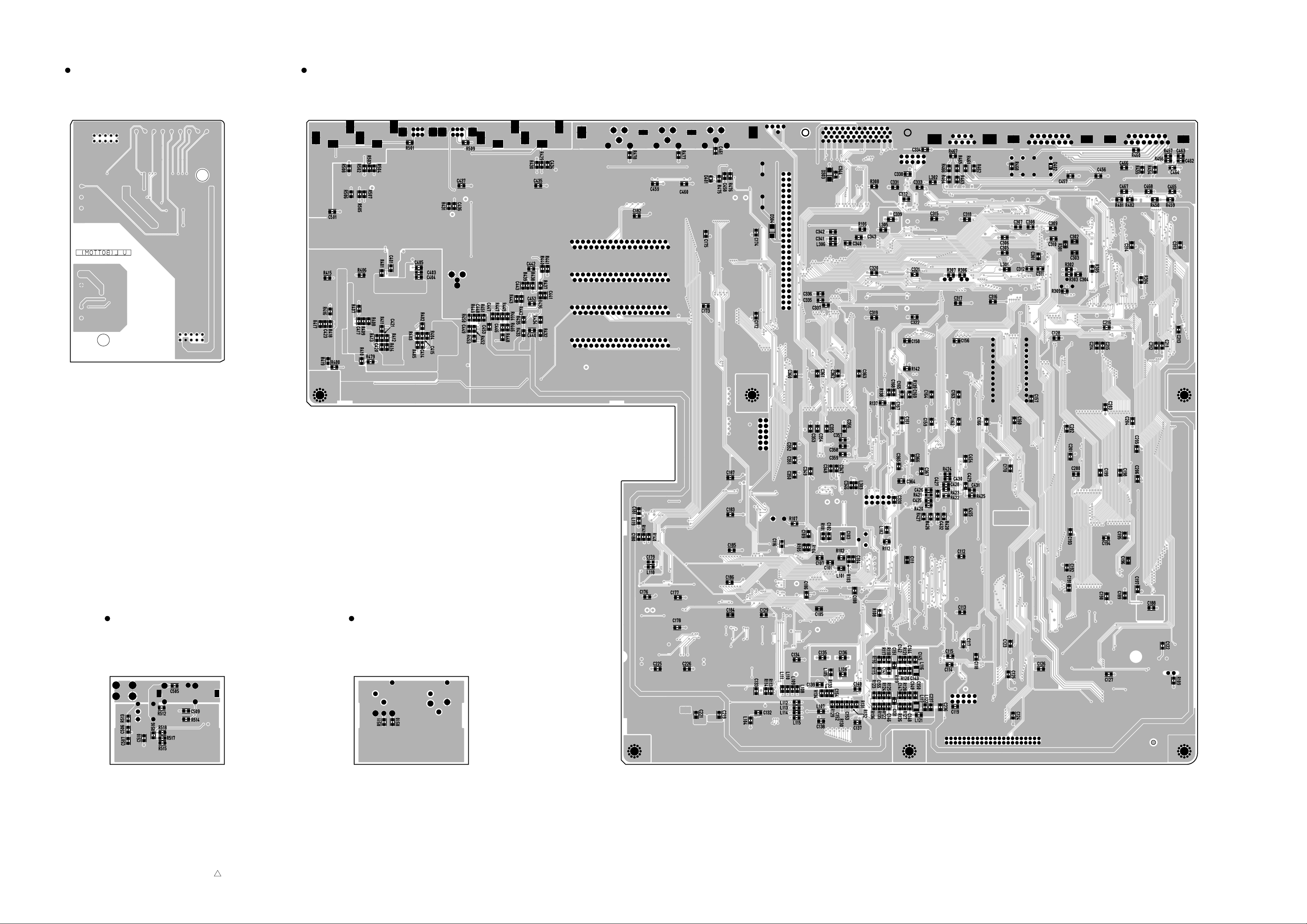
MAIN-A, MAIN-B, MAIN-C: 3NA-V312430-3
S-SYNC: 3NA-V519530-2
2
Pattern side Pattern side Pattern side
Pattern side
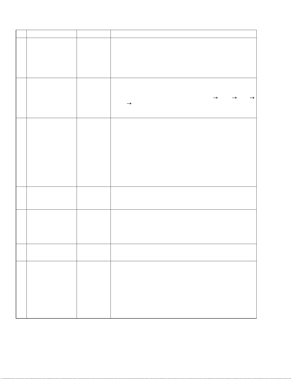
MAIN-A Circuit BoardS-SYNC Circuit Board
MAIN-B Circuit BoardMAIN-C Circuit Board
D24
36
Note: See parts list for details of circuit board component parts.
Page 2
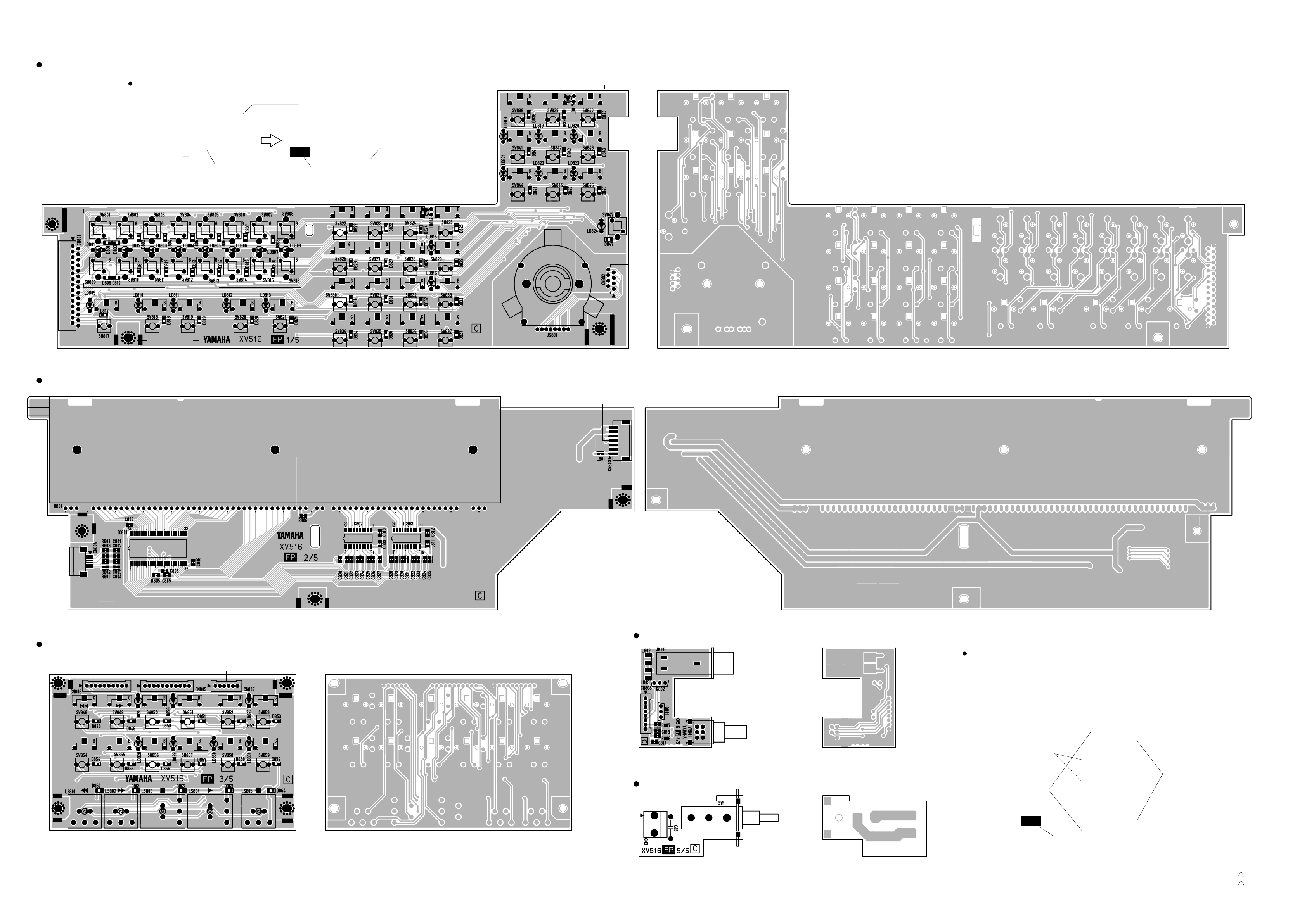
FP 1/5–5/5: 3NA-V312440-2
3NA-V312440-3
5
5
Pattern sideComponent side
Pattern sideComponent side
Component side Pattern side
Component side Pattern side
Pattern side
Component side
RECORD READY
12345678
897
564
231
0/-
1 234567 8
to SUB(PANEL)-CN705
to SUB(PANEL)-CN703
to PS2/2-CN8
Light touch switch
G=Glay
B=Black
Push button
(VT810300) or
(VT839000)
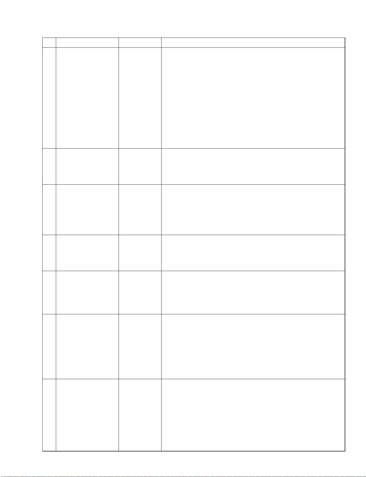
FP1/5 Circuit Board
FP2/5 Circuit Board
FP3/5 Circuit Board
Push Button installation
FP 4/5 Circuit Board
FP 5/5 Circuit Board
PHONES
PHONES
LEVEL
to MAIN A-CN108to PS 1/2-CN11
POWER
REHE
REPEAT
ROLL
BACK
AB
SET
AUTO
PUNCH
OUTIN
to SUB(PANEL)
-CN707
LAST REC
PROJECT SEARCH
RTN TO ZERO
Jog shuttle
(VR625800)
Jog cover
(V3287700)
Knob
FP
Jog Suttle
FP 1/5
to SUB(PANEL)
-CN706
to SUB(PANEL)
-CN708
SOLO/SELECT
AUTO
INPUT
PEAK
HOLD
ALL
INPUT
FORMAT CHASE
CANCEL ENTER LOCATE
JOG/
DATA
JOG ON
TIME DISPLAY
V.TRACK
SELECT
EDIT UNDO/
REDO
VARI
SPEED
UTILITY
SET
UP
CAP-
TURE
ABS/
REL
RE-
MAIN
to SUB(PANEL)-CN704
SHUTTLE/
CURSOR
LOC MEM STORE
LOC MEM RECALL
PROJECT SELECT
MONITOR SELECT
D24
37
Note: See parts list for details of circuit board component parts.
Page 3
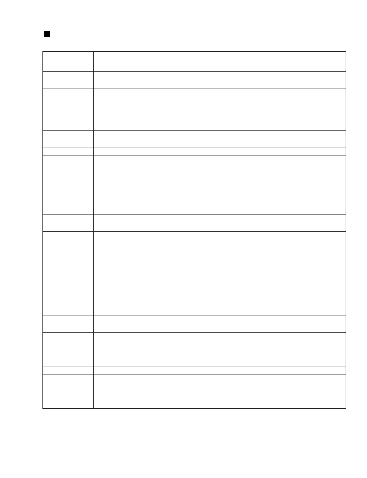
ERROR MESSAGES
D24
38
If the D24 displays an error message, follow the instructions below.
Message
Sync no comm
TC not read
WC not read
FILE ERROR
DEV CONT ERR
SCSI BREAK n
FIFO UO ERR n
INVALID COM n
PARITY ERR n
SCSI OUT n
SCSI ERR nn
MEDIA ERR nn
DRIVE ERR nn
REC ERROR
TOO SHORT
DISK FULL
FS DIFFER
RECCH NOTSEL
MO PROTECT
PROJ PROTECT
DATA FULL
Meaning
The slave machine is not connected properly.
The timecode source cannot be read properly.
The wordclock source cannot be read properly.
The MO disk data is not correct.
SCSI communication error. External device
connection.
SCSI communication error. Command break.
SCSI communication error. FIFO under/over.
SCSI communication error. Invalid command.
SCSI communication error. Parity error.
SCSI communication error. Time out.
SCSI error. SCSI error other than those listed
above.
Error due to media.
Error due to media or drive.
An incorrectly recorded track has been detected
and its contents may be distorted. This message
may appear after recording on a disk containing
heavily edited tracks and is due to the D24’s
disk drive not been able to keep up with the
excessive workload.
The interval between the points is too short.
There is no space available for storing sound
files.
Recording is not possible because the sampling
rate of the selected project is not the same as
the cur-rent D24 setting.
No tracks are selected for recording.
The disk is write protected.
The project is write protected.
There is no space available for storing project
management files.
Remedy
Check the connections to the slave machine.
Check the timecode settings.
Check the wordclock settings.
Follow the instructions on the display. If “TURN OFF”
is displayed, turn the D24 off and then on again.
Follow the instructions on the display.
Follow the instructions on the display.
Follow the instructions on the display.
Follow the instructions on the display.
Follow the instructions on the display.
Follow the instructions on the display.
Follow the instructions on the display.
Try the following:
1) Clean the media or disk drive head.
2) Physically reformat the disk. If the error persists,
change the media.
Reload the disk. If the error persists, change the media.
If that doesn’t fix it, the drive may be broken.
Press the [UNDO] button to undo the last recording,
reduce the number of tracks selected for simultaneous
recording, and try recording again. Temporarily
assigning unused virtual tracks to main tracks is another
way to reduce the D24’s workload.
For part editing, the minimum interval between the start
and end points is 15 ms. For punch in/out recording, the
minimum interval is 15 ms. Increase the interval as
necessary.
Retrieve some disk space by using the Optimize function.
Delete or erase an unwanted project.
Set the sampling rate on the D24 to match that of the
project.
Select a track for recording.
Turn off the write protection.
Turn off the write protection.
Retrieve some disk space by using the Optimize
function.
Delete or erase an unwanted project.
Page 4
SETTING THE SCSI ID
D24
39
Setting the SCSI ID of the internal MO disk drive involves removing the D24’s top cover and setting the DIP
switch located on the MO drive’s circuit board.
1 Remove the top-cover fixing screws (11), as
shown here.
2 Remove the top cover.
3 Using a small flat-bladed screwdriver, or
something similar, set DIP switches 1 through 3,
as listed below, to achieve the required SCSI ID.
SCSI IDs 6 and 7 are not listed, since they are reserved for other purposes.
SCSI ID
5
4
3
2 (default)
1
0
DIP switch number
1
ON
ON
OFF
OFF
OFF
OFF
2
OFF
OFF
ON
ON
OFF
OFF
3
ON
OFF
ON
OFF
ON
OFF
Page 5
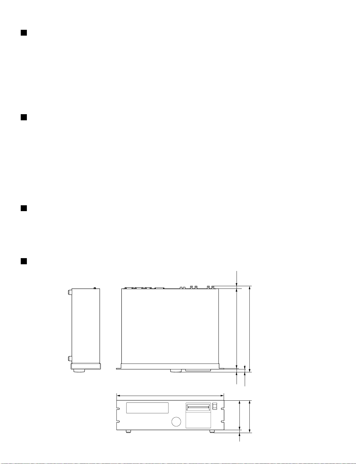
W: 480
Units: mm
12 132
12.9
4.1
H: 144 D: 383.9
355.1 11.8
D24
40
INITIALIZE
You can reset the D24 to its initial settings as follows.
1 Turn off the D24 Power switch.
2 While holding down the [RTN TO ZERO] button, turn on the D24 Power switch.
The D24 is initialized and “INITIALIZED” appears on the display.
CHECKING THE VERSION NUMBER
You can check the version number of the D24 system software as follows.
1 Turn off the D24 Power switch.
2 While holding down the [UTILITY] button, turn on the D24 Power switch.
The version number appears on the display.
UPDATING THE SYSTEM SOFTWARE
DIMENSIONS
See the Yamaha Professional Audio Web site at the address below for information on system updates.
<http://www.yamaha.co.jp/product/proaudio/homeenglish/>
Page 6
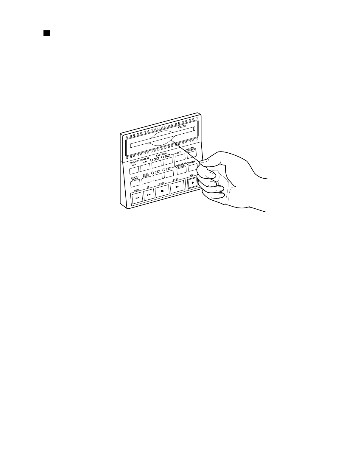
EJECTING TROUBLESOME DISKS (EMERGENCY USE)
D24
41
If the D24 is turned off inadvertently, or the disk loading mechanism fails, you may not be able to eject a disk in
the normal way. In this case, the disk can be ejected using the supplied disk eject tool. Note that this technique
should only be used as a last resort, as frequent use may lead to malfunction.
1 Turn off the D24 Power switch.
2 Insert the disk eject tool into the manual eject hole, as shown below, and push gently to eject the disk.
3 The disk ejects.
Page 7
D24
42
TEST PROGRAM
1. Measuring Conditions
• Unless specifically indicated, the unit is in the no MO DISC mode.
• All switches are set to OFF and the [PHONES LEVEL] is set to “0”
<Input Signal>
• With the MY8-AD card mounted in [SLOT 1], input a 1 kHz-10 dBmsine wave.
• Use the stereo plug to connect a 40 Ω load to the PHONES terminal.
2. Check Initial Operation of Main Circuit Board
With POWER ON, check that the CPU RUN indicator LEDs mounted on the MAIN-A circuit board are flashing.
GUI CPU & peripheral I/O: D101 (Red LED at front left side of main sheet.)
MEDIA CPU & peripheral I/O: D302 (Red LED at rear left side of main sheet.)
TIDSP & peripheral I/O: D301 (Green LED at rear left side of main sheet.)
3. Communication Inspection Between MAIN Circuit Board SUB Circuit Board
With POWER ON, check that OK is displayed on the fluorescent display tube.
Example:
4. Check ROM Version
Hold down the [Utility] key when turning on the power to display the ROM version in the fluorescent display tube.
(**.**is the version number)
5. Test Program
<Measuring Device>
Low-frequency oscillator, AC voltmeter, distortion meter, MY Card, SCSI compatible HDD (there are model restrictions),
device with VIDEO OUT, D24
<Preparations>
• Connect the inspection equipment (FAT D24) and main unit [TIME CODE IN/OUT] connector with a CANNON cable.
• Connect the inspection equipment (FAT D24) and main unit [SYNC IN/OUT] connector with D-SUB 15 PIN cable.
• Connect the [COAXIAL IN/OUT] connectors with RCA PIN cable.
• Connect the [MIDI IN/OUT] connectors with MIDI cable.
• Connect the D-SUB 9 PIN plug (Pin) connector for inspection to the [SERIAL I/O] connector. (Connect between 3
Pin 7 Pin and 2 Pin 8 Pin)
<Start>
Hold the [SETUP] key and turn on the power to enter the test program. The following will be displayed on the fluorescent
display tube.
(Due to MO mount processing, key entry is not accepted until
after normal operation has started, approximately 10 seconds.)
<Test Procedure>
Select test items: Use the keypad to enter the test item number. Press [ENTER] to execute the test.
Test result determination: The determination of each test item will be displayed as “OK” or “NG” in the fluorescent
tube display.
Interrupting the test: Press [CANCEL] to interrupt a test in progress. (If it is being used for test determination,
press [CANCEL] once again.)
YAMAHA D24, SCSI-IO OK ···
D24 V**.
**
00 DIAG RDY
Page 8
D24
43
00
01
02
03
04
05
06
07
08
Play output system
check
Software version
information
GUI-CPU peripheral
operation
TI-DSP peripheral
operation
Media CPU peripheral
operation
Fluorescent tube
display
Switch/LED display
JOG/SHUTTLE input
COAXIAL I/O (Status)
01 VNO G***
M*** U***
02 G-CPU
03 TI DSP
04 M-CPU
05 VFD
06 SW
***
07 JOG 00
SHU 00
08 COAX1
No. Test Item Display Test Functions and Judgment Criteria
When the Media CPU sine wave program (1 CH=500 Hz, 6 CH= 440 Hz -3
dB) starts there is output to the output CH lines for the 1 CH, 6 CH for
[PHONES], [SLOT 1– 4]. The output terminals for these are measured.
The determinations are as follows.
(1) Display on fluorescent tube display: [WC]INT, [FS]48K, [BIT]24,
[TC]MASTER.
(2) Level meter display: 1 TR, 6 TR both display -3 dB.
(3) PHONE OUT: Asound can be heard on the
headphones or by waveform
observation. (L=500 Hz, R=440 Hz
40 ΩLoad 2.5 Vp-p)
(4) SLOT OUT: Check output of MY Card.
Checks the version of the software that has been installed for use by the G
(GUI CPU), M (Media CPU) and U (Panel CPU). (Check by the number
displayed in the * * * section.)
Checks the operation of peripheral devices the GUI-CPU is controlling.
OK or NG is displayed.
Checks the operation of peripheral devices the TI-DSP is controlling.
OK or NG is displayed.
Checks the operation of peripheral devices the Media CPU is controlling.
OK or NG is displayed.
Checks that each segment of the fluorescent tube display lights in sequence.
After all segments have been lit, press the [ENTER] key. An OK will be
displayed. If an abnormality occurs, press [CANCEL]. A NG will be
displayed and the test will be interrupted.
Checks the operation of the front panel switches and the lighting of the LEDs.
When the key displayed in the *** section of the fluorescent tube display is
pushed, the name of the key for the next test will be displayed if there has
been proper operation. If the switch has an LED, it also checks that the LED
lights when the key is pushed. When the check for all switches has been
completed, an OK is displayed.
If there is an abnormality or if the test is to be interrupted, press the [REC]
key. A NG will be displayed and the test will be stopped.
Checks that each data display is displaced by the title operation of [JOG]
and [SHUTTLE].
(1) JOG data displacement value
In + direction (clockwise) hexadecimal display:
00 01 02 FF 00 01 02
In - direction (counterclockwise) hexadecimal display:
00 FF FE 01 02 FF FE
(2) SHUTTLE data displacement value
In + direction (clockwise) hexadecimal display:
00 01 02 03 04 05 06 07
In - direction (counterclockwise) hexadecimal display:
00 FF FE FD FC FB FA F9
After all data displacement values have been checked, press the [ENTER]
key and an OK is displayed. If there is an abnormality, press the [CANCEL]
key. A NG will be displayed and the test will be stopped.
Checks the sending and receiving of channel status signals.
If normal, an OK is displayed. If there is an abnormality, NG will be displayed
and the test will be stopped.
Test Items
Page 9
D24
44
09
10
11
12
13
14
15
System clock (FS)
detection
VARI SPEED
Variable operation
RTC operation, Date
registration
SERIAL I/O
REMOTE/SYNC I/O
VIDEO IN
TIME CODE OUT
09 FS
10 VARI
11 RTC
********
12 SERIAL
13 REMOTE
14 VIDEO
15 TC OUT
00:00:00:00
No. Test Item Display Test Functions and Judgment Criteria
Checks the result of the automatic measurement of the oscillating frequency of
the FS signals (44.1 kHz, 48.0 kHz) for the internal system clock generator.
First it measures the frequency of the 44.1 kHz signal, then the frequency
of the 48.0 kHz signal. If both frequencies are normal, an OK is displayed.
If there is an abnormality, a NG is displayed. In addition, it also checks that
“44.1 K” and “48 K” are lit in the FS area of the fluorescent display tube after
each signal frequency has been measured.
Automatically measures and checks the FS signals (44.1 kHz, 48.0 kHz)
oscillating frequencies at 5 step settings.
First it measures the frequency of the 44.1 kHz signal settings, then the frequency of
the 48.0 kHz signal settings at each of the 5 steps (-6.00% -3.00% 0.00%
+3.00% 6.00%), automatically makes the settings and measures the oscillating
frequency at each step. If both frequencies are normal, an OK is displayed.
If there is an abnormality, NG will be displayed and the test will be stopped.
Checks the date registration and operation of the Real Time Clock.
Date recording: Press the [CANCEL] key and all the data in the *** section
will be displayed as “0”. Use the keypad to enter the date in
AD format in the following sequence: year / month / day /
hour / minute / seconds. Press the [Enter] key to set. (In the
AD format, only the last two digits are entered. The entry for
May 6, 2000 at 15 minutes and 9 seconds past 3 o’clock
(3:15:09 PM) would appear as “000506151509”.
When the [ENTER] key is pushed and the date is registered, check that the
seconds display has started counting. When the [ENTER] key is pushed
again, an OK is displayed. If there is an abnormality, NG will be displayed
and the test will be stopped.
Checks that the SERIAL signal (RS-422) is being sent and received.
Prior to the test, connect the inspection connector (D-SUB 9 PIN) to the
[SERIAL IN/OUT] connector. If it is normal an OK is displayed. If there
is an abnormality, NG will be displayed and the test will be stopped
Checks that the SERIAL signal for REMOTE/SYNC (RS-485) is being
sent and received.
Prior to the test, connect a D-SUB 15 PIN cable to the inspection equipment
(FAT D24) and [SYNC IN/OUT] connector of the main unit. If it is normal,
an OK is displayed. If there is an abnormality, NG will be displayed and the
test will be stopped.
Checks the operation of the VIDEO vertical synchronization signal count function.
If it is normal, an OK is displayed. If there is an abnormality, NG will be
displayed and the test will be stopped.
Checks the output of the Time Code Generator.
Prior to the test, connect a CANNON cable to the inspection equipment (FAT
D24) and the [TIME CODE IN/OUT] connector on the main unit. When the
test is started, the receiving time data display on the fluorescent display tube
starts to count upward. When the test program for the inspection equipment
(FAT D24) is started and Test No. 16 is executed, the receiving time data on
the inspection equipment and the receiving time data on the main unit display
the same time and the counting up of the data is checked. The [ENTER] key
on the main unit is pushed. If the test is normal, an OK is displayed. If there is
an abnormality, NG will be displayed and the test will be stopped.
Page 10
D24
45
16
17
18
19
20
21
22
TIME CODE IN
SCSI operation
SLOT
Data initialize
EXIT
(Inspection
completed)
SYNC MASTER
SYNC SLAVE
16 TC IN
XLR
00:00:00:00
17 SCSI
18 BAY IO
SLOT 1 ENTER
19 INIT RDY
20 EXIT
21
SYNC-M ***
22
SYNC-S ***
No. Test Item Display Test Functions and Judgment Criteria
Checks the Time Code Reader input.
Prior to the test, connect a CANNON cable to the inspection equipment (FAT
D24) and the [TIME CODE IN/OUT] connector on the main unit. When the
test program is started on the inspection equipment (FAT D24) and Test No.
15 is executed, the receiving time data display on the fluorescent display tube
starts to count upward. The receiving time data on the inspection equipment
and the receiving time data on the main unit display the same time and the
counting up of the data is checked
Next, push the [ENTER] key on the main unit and the XLR display on the
fluorescent display tube will change to RMT. Also at this time, the receiving
time data on the inspection equipment and the receiving time data on the main
unit display the same time and the counting up of the data is checked.
Push the [ENTER] key one more time. If the test is normal, an OK is displayed.
If there is an abnormality, NG will be displayed and the test will be stopped.
Checks the internal and external SCSI operations.
Prior to the test, connect a SCSI cable to the HDD that is D24 operation
guaranteed (one that has been formatted in the normal mode). (The SCSI
ID is “0” or “1”.) If the test is normal, an OK is displayed. If there is an
abnormality, NG will be displayed and the test will be stopped.
Checks the connection of the SLOT for MY Card.
Prior to the test, mount MY SLOT CHECK CARD in [SLOT 1-4]. Press the
[ENTER] key and [SLOT 1] is checked. If it is normal, OK and GO TO
SLOT 2 will be displayed. The check then moves to [SLOT 2]. This same
process is also carried out for [SLOT 3] and [SLOT 4]. If all connections are
normal, an OK is displayed. If there is an abnormality, NG will be displayed
and the test will be stopped.
Initializes basic data with exception of date data.
Once this test is started, the RDY display section of the fluorescent display
tube will flash. Press the [ENTER] key to execute the initialization. To
interrupt the test, press [CANCEL]. A NG will be displayed and the test will
be stopped.
Removes unit from test mode and restores it to standard mode.
Press the [ENTER] key and if all test items have been completed, an OK will
be displayed. After a few seconds, the unit will be in the same mode as it is
after POWER ON. If one of the test items has not been completed, a NG will
be displayed. Press the [CANCEL] key to return to the test mode and execute
the incomplete tests.
Checks the output of the SYNC MASTER.
Prior to the test, connect a D-SUB 15 PIN cable to the inspection equipment
(FAT D24) and [SYNC IN/OUT] connector of the main unit. Start the test
program for the inspection equipment (FAT D24) is started and Test No. 22.
Each time the [ENTER] key is pushed on the main unit, the *** section display
on both the main unit and the inspection equipment will start to count up
simultaneously and can be checked.
Press the [CANCEL] key on the main unit. If the test is normal, an OK is displayed.
If there is an abnormality, NG will be displayed and the test will be stopped.
Checks the SYNC SLAVE input.
Prior to the test, connect a D-SUB 15 PIN cable to the inspection equipment
(FAT D24) and [SYNC IN/OUT] connector of the main unit. The test
program is started on the inspection equipment (FAT D24) and Test No. 21
is executed. Each time the [ENTER] key is pushed on the test equipment,
the *** section display on both the main unit and the inspection equipment
will start to count up simultaneously and can be checked.
Press the [CANCEL] key on the inspection equipment. If the test is normal, an
OK is displayed. If there is an abnormality, NG will be displayed and the test
will be stopped.
Page 11

D24
46
23
24
25
26
27
28
29
30
31
32
40
99
SYNC 8FS
EXT WORD CLOCK
IN
PHONE OUT-1
PHONE OUT-2
PHONE OUT-3
PHONE OUT-4
Switches SLOT input
COAXIAL INPUT
AES CH STATUS
COAXIAL CH
STATUS
Inspection support
mode
EXIT
(Forced termination)
23 SYNC-F
24 WC IN
25 OSC-1
26 OSC-2
27 OSC-3
28 OSC-4
29 SLOT
30 COAX
31 AES
C/S A100200
32 COAX
C/S 00000000
40
MASTER OK
No. Test Item Display Test Functions and Judgment Criteria
Checks the connection signal of the 8FS interrupt signal.
If the test is normal, an OK is displayed. If there is an abnormality, NG will
be displayed and the test will be stopped.
Checks the synchronizing function of the [WORD CLOCK INPUT] signal.
Displays the following on the fluorescent display tube for checking.
[LOCK]: Lights.
[WC] Column: EXT lights.
[FS] Column: 44.1 or 48 K lights. (input WORLD CLOCK frequency)
Push the [CANCEL] key. If the test is normal, an OK is displayed. If there
is an abnormality, NG will be displayed and the test will be stopped.
Check [PHONES] CH1/CH2 output.
Check the output from the [PHONES] by the sound in the headphones.
Check [PHONES] CH3/CH4 output.
Check the output from the [PHONES] by the sound in the headphones
Check [PHONES] CH5/CH6 output.
Check the output from the [PHONES] by the sound in the headphones
Check [PHONES] CH7/CH8 output.
Check the output from the [PHONES] by the sound in the headphones
Checks the input of [SLOT 1-4].
Each press of the [ENTER] key switches the [SLOT]. The absence or presence
of a signal is displayed at the level meter display of the fluorescent display tube
and a [PHONES] output sound can be heard.
After checking up to [SLOT 4], press the [ENTER] key once again. If the
test is normal, an OK is displayed. If there is an abnormality, NG will be
displayed and the test will be stopped.
Checks input signal of [COAXIAL INPUT].
Press the [ENTER] key. The absence or presence of a signal is displayed at
the level meter display of the fluorescent display tube and a [PHONES]
output sound can be heard. If the input is normal, an OK is displayed. If there
is an abnormality, NG will be displayed and the test will be stopped.
Checks the STATUS data of the AES CARD (MY-4) input signal.
Press the [ENTER] key. The flashing A100200 display on the fluorescent
display tube will stop and OK will be displayed. If no signal has been detected,
NG will be displayed and the test will be stopped.
Checks the STATUS data of the COAXIAL input signal.
Press the [ENTER] key. The flashing 00000000 display on the fluorescent
display tube will stop and OK will be displayed. If no signal has been detected,
NG will be displayed and the test will be stopped.
This mode has been provided for inspecting while linked to input and output
of the [TIME CODE INPUT/OUTPUT] etc. It receives the MIDI Program
change from the main unit subject to inspection and the corresponding test
items can be started. It can be ended by turning on the power again or by
pressing the [CANCEL] key.
Removes unit from test mode and restores it to standard mode.
Page 12

D24
47
YAMAHA [Digital Multitrack Recorder] Date: 18 Feb 1999
Model: D24
MIDI Implementation Chart
Version: 1.0
Function... Transmitted Recognized Remarks
Basic
Channel
Default
Changed
X
X
X
X
Mode
Default
Messages
Altered
X
X
**************
X
X
X
Note
Number True Voice
X
**************
X
X
Velocity
Note On
Note Off
X
X
X
X
After
Touch
Keys
Ch’s
X
X
X
X
Pitch bend X X
Control
Change
Prog
Change :True#
X
**************
X
XX
X
System Exclusive X O *1
System
Common
:Song Pos
:Song Sel
:Tune
X
X
X
X
X
X
System
Real Time
:Clock
:Commands
X
X
X
X
Aux
Messages
:Local ON/OFF
:All Notes OFF
:Active Sense
:Reset
X
X
X
X
X
X
X
X
Notes
MTC quarter frame messages are received in MTC Sync slave mode
MTC quarter frame messages are transmitted in MTC Sync master
mode.
*1: MMC
Mode 1: OMNI ON, POLY
Mode 3: OMNI OFF, POLY
Mode 2: OMNI ON, MONO
Mode 4: OMNI OFF, MONO
O: Yes
X: No
Page 13

CONTENTS
OVERALL ASSEMBLY······························································································································ 2
FRONT ASSEMBLY··································································································································4
POWER SUPPLY ASSEMBLY ················································································································· 5
ELECTRICAL PARTS ·························································································································6~17
PARTS LIST
WARNING
Components having special characteristics are marked and must be replaced with parts having
specification equal to those originally installed.
A: Australian model
B: British model
C: Canadian model
D: German model
E: European model
F: French model
H: North European model
I : Indonesian model
J: Japanese model
M: South African model
O: Chinese model
Q: South-east Asia model
T: Taiwan model
U: U.S.A. model
V: General export model (110 V)
W: General export model (220 V)
N,X:General export model
Y: Export model
Notes : DESTINATION ABBREVIATIONS
• The numbers in “ QTY ” show quantities for each unit.
• The parts with “ - - ” in “ PART NO. ” are not available as spare parts.
• The mark “ ” in the remarks column indicates that these parts are interchangeable.
• The second letter of the shaded ( ) part number is O, not zero.
• The second letter of the shaded ( ) part number is I, not one.
DIGITAL MULTITRACK RECORDER
Page 14

D24
2
OVERALL ASSEMBLY
650
600
660
710
680
210
370
380
390
350
200
180
160
190
720
140
310
210
300
130
150
120
440
440
430
540
270
550
500
800
250
240
340
10b
10
10c
10f
10d
10f
10e
10e
10g
10g
10a
10h
100
700
60
70
330
110
450
420
480
410
40
80
90
50
30
20
580
570
560
510
530
400
A
420
440
480
440
410
260
520
670
450a
450b
450c
300a
360c
360b
300b
360a
330
900
800
810
Power Supply
Assembly
(See page 5.)
Front Assembly
(See page 4.)
660
Page 15

3
D24
OVERALL ASSEMBLY
Overall Assembly
Overall Assembly
Overall Assembly
Overall Assembly
Circuit Board
Sub Assembly
Sub Assembly
Sub Assembly
Partition
Power Transformer
Power Transformer
Power Transformer
Bind Head Tapping Screw-B
Recorder Unit
Angle
Bind Head Screw
Bind Head Tapping Screw-B
Spacer
YGDI Angle
Bind Head Tapping Screw-B
Circuit Board
Bind Head Tapping Screw-B
Stay
Bind Head Tapping Screw-B
Side Panel
Bind Head Tapping Screw-B
Side Panel
Bind Head Tapping Screw-B
Rear Panel
Rear Panel
Rear Panel
Fan
Finger Guard
Fan Angle
Pan Head Screw
Bind Head Tapping Screw-B
Bind Head Screw
Bind Head Tapping Screw-B
Bind Head Tapping Screw-B
Circuit Board
Circuit Board
Bind Head Tapping Screw-B
Power Supply Assembly
Power Supply Assembly
Bind Head Tapping Screw-B
Connector Assembly
Ferrite Core
AC-IN Connector
Bind Head Tapping Screw-P
Cord Holder
Cord Holder
Bind Head Screw
Bind Head Screw
Circuit Board
Circuit Board
Circuit Board
Jack Socket
Pan Head Screw
Bind Head Tapping Screw-B
Bind Head Tapping Screw-B
Angle
Flat Head Tapping Screw-B
Front Assembly
Bind Head Tapping Screw-B
Bottom Assembly
Bottom Cover
Foot
Bind Head Tapping Screw-B
Bind Head Tapping Screw-B
DESCRIPTION
A
10
10
10
10a
10b
10b
10b
10c
10d
10e
10f
10g
10h
20
30
40
50
60
70
80
90
100
110
120
120
120
130
140
150
160
180
190
200
210
240
240
250
260
260
270
300
300a
300b
310
330
330
340
350
360a
360b
360c
370
380
390
400
410
420
430
440
450
450a
450b
450c
480
REF NO.
- -
- -
- -
- -
V5195300
- -
- -
- -
- XU676A00
XU677A00
XU678A00
VC688800
V3125400
V3103700
VP156600
VP157000
- -
- VC688800
V3268800
EP600190
- VC688800
V3101500
VC688800
V3101600
VC688800
V3101800
V3101900
V3102000
V3125300
VN003900
VM964700
VR116500
VP157000
VP156600
VP157000
VC688800
V3268200
V3268400
EP600190
V3117900
V3124900
VD831800
- VC362700
VL785200
VC161100
CB069250
CB069250
EG340360
VP156600
NX820720
NX820730
NX820740
VT362500
VT267800
VP157000
EP600190
V3103800
VP063700
- VC688800
V3496600
- CB651110
VS756600
VC688800
PART NO.
S-SYNC
UL CSA
CEE
A4.0X8 MFZN2BL
MCB3064SS
A3.0X6 MFZN2BL
A3.0X8 MFZN2BL
4.0X8 MFZN2BL
SUB(BAY)
3.0X8 MFZN2BL
4.0X8 MFZN2BL
LEFT
4.0X8 MFZN2BL
RIGHT
4.0X8 MFZN2BL
MMS-06E12DL
FG-06ULB
SP 4.0X25 MFZN2BL
3.0X8 MFZN2BL
3.0X6 ZMC2BL
3.0X8 MFZN2BL
4.0X8 MFZN2BL
PS 1/2
PS 1/2
3.0X8 MFZN2BL
4.0X12 MFZN2BL
ACIN ASSY 0
FR25/15/12-1400L
AC AC-P01CR02
3.0X12 ZMC2BL
BK-1
BK-1
4.0X8 MFZN2BL
3.0X6 MFZMC2BL
MAIN A
MAIN B
MAIN C
17L-003A3
2.6X6 MFNI33
3.0X8 MFZN2BL
3.0X8 MFZN2BL
4.0X10 MFZN2BL
4.0X8 MFZN2BL
TL-014
3.0X14 MFZN2B
4.0X8 MFZN2BL
D24 J,U,C,V,H,W,B
J (V309960)
U,C,V (V309970)
H,W (V309980)
B (V309990)
J (V325920)
U,C,V (V325930)
H,W,B (V325940)
(V310120)
J
U,C,V
H,W,B
(V413330)
(V310130)
(V310140)
J
U,C,V
H,W,B
J,U,C,V
H,W,B
J,U,C,V
H,W,B
AC IN (V325380)
J
U,C,V,H,W,B
(V311770)
(V310390)
REMARKS
4
2
4
4
2
2
4
8
3
3
3
4
4
5
4
2
2
11
12
4
6
2
2
6
2
4
5
4
4
11
QTY
RANK
*
*
*
*
*
*
*
*
*
*
*
*
*
*
*
*
*
*
*
*
*
*
*
01
01
01
01
01
01
01
01
05
09
01
01
01
01
01
01
01
04
03
01
01
01
01
01
01
01
01
01
01
01
02
01
Connector Assembly
Connector Assembly
Connector Assembly
Connector Assembly
Connector Assembly
Connector Assembly
KR Connector Assembly
KR Connector Assembly
Connector Assembly
FFC Cable
FFC Cable
Top Cover
Bind Head Tapping Screw-B
IF Plate
Bind Head Screw
Label
Label
Label
Label,Date Coad
Label,Date Coad
Holder
Holder
Ferrite Core
ACCESSORIES
MO Disk
Adapter, AC Cord
AC Cord
AC Cord
AC Cord
AC Cord
DESCRIPTION
500
510
520
530
540
550
560
570
580
590
600
650
660
670
680
700
700
710
720
720
800
810
900
REF NO.
- -
- -
- -
- -
- -
V3254300
- -
- V3261800
V3583900
V3116600
V3104000
VC688800
VZ678500
VP156900
- -
- -
- -
- -
- CB835590
CB825280
VC362700
- VQ240200
VT119800
VB927800
VB928000
VP204400
PART NO.
PSW ASSY
PS-MAIN ASSY
PH&PH 12P 500L
PH&PH 8P 160L
PH&PH 5P 250L
MO ASSY
6 160mm C&C 2mm
5 160mm C&C 2mm
MAIN TO MO D24
P=1.0-K-5-80
P=1.25-K-36-170
4.0X8 MFZN2BL
4.0X12 MFZN2BL
CAUTION A
CAUTION B
CAUTION C
TMS-20
CKN-05
FR25/15/12-1400L
RO-M640
KPR-25
J 7A 125V 3P 2.5m
CSA
VDE
BS 3
(V314570)
(V412780)
(V325400)
(V325410)
(V325420)
(VR78720)
(VR78550)
U,C,V (V332560)
H,W (V332570)
U,C,V (V333500)
U,C,V (VA03930)
H,W (CB07612)
U,C,V,H,W,B
(V360310)
J
J
U,C,V
H,W
B
REMARKS
4
11
4
8
2
QTY
RANK
*
*
*
*
*
01
05
01
01
01
04
06
06
08
08
10
*
:
New Parts RANK: Japan only
*
:
New Parts RANK: Japan only
Page 16

4
D24
FRONT ASSEMBLY
Front Assembly
Front Panel
Escutcheon, Power Switch
Window
Sub Chassis
Bind Head Screw
Hexagonal Nut
Circuit board
Circuit board
Circuit board
Circuit board
Circuit board
Bind Head Tapping Screw-B
Bind Head Tapping Screw-B
Sub Panel
Bind Head Tapping Screw-B
Bind Head Tapping Screw-B
Circuit Board
Bind Head Tapping Screw-B
Power Switch Knob
Knob
Bind Head Tapping Screw-B
Spacer
Adhesive Tape
FFC Cable
FFC Cable
FFC Cable
Connector Assembly
Cranp
JOG Cover
Cord Holder
Cushion
DESCRIPTION
10
20
30
40
60
70
110a
110b
110c
110d
110e
120
140
150
170
180
190
200
210
220
250
260
270
300
310
320
330
480
490
500
510
REF NO.
- V3114300
VL813000
V3114400
- VP156600
V2431400
NX820670
NX820680
NX820690
NX820700
NX820710
EP600190
EP600190
V3114900
EP600190
EP600190
V3268700
EP600190
VL812900
VQ920800
VC688800
- -
- V3583700
V3266100
V3583800
- CB825280
V3287700
CB069250
- -
PART NO.
3.0X6 MFZN2BL
9.0
FP 1/5
FP 2/5
FP 3/5
FP 4/5
FP 5/5
3.0X8 MFZN2BL
3.0X8 MFZN2BL
3.0X8 MFZN2BL
3.0X8 MFZN2BL
SUB(PANEL)
3.0X8 MFZN2BL
L GY /D GY
4.0X8 MFZN2BL
P=1.0-K-6-80 BNCD
P=1.25-K-8-80 BNCD
P=1.25-K-30-80 BNCD
PH&PH 7P 160L
CKN-05
BK-1
D24
(V311770)
(V311460)
POWER
PHONES LEVEL
(V413330)
(CB55090)
(VR92670)
(V453250)
REMARKS
2
3
5
4
4
2
2
2
QTY
RANK
*
*
*
*
*
*
*
*
*
*
*
*
*
03
01
01
01
01
01
01
01
03
03
01
01
03
01
*
:
New Parts RANK: Japan only
FRONT ASSEMBLY
110b
500
40
300
200
190
310
60
210
180
270
260
330
120
140
260
490
150
180
170
250
510
30
10
20
250
220
70
320
480
110e
110d
110a
110c
Page 17

D24
5
POWER SUPPLY ASSEMBLY
60
120
60
120
50
90
20
80
10
70
30
100
40
POWER SUPPLY ASSEMBLY
Power Supply Assembly
Power Supply Assembly
Heat Sink
Insulation Sheet
Heat Sink
Insulation Sheet
Circuit Board
Circuit Board
Bind Head Tapping Screw-B
TR holder (A)
Bind Head Tapping Screw-B
TR Holder (B)
Bind Head Tapping Screw-B
Spring Washer
DESCRIPTION
10
20
30
40
50
50
60
70
80
90
100
120
REF NO.
V3117900
V3124900
- -
V3115100
- V3115900
V3268300
V3268500
EP600190
- VP157000
- VP157000
03765160
PART NO.
A
B
B
PS 2/2
PS 2/2
3.0X8 MFZN2BL
3.0X8 MFZN2BL
3.0X8 MFZN2BL
#2 M3.0
D24
J,U,C,V
H,W,B
(V311500)
(V326940)
J,U,C,V
H,W,B
(V311560)
(V311600)
REMARKS
5
3
2
2
QTY
RANK
*
*
*
*
*
*
01
01
01
*
:
New Parts RANK: Japan only
Page 18

D24
6
ELECTRICAL PARTS
Circuit Board
Circuit Board
Circuit Board
Circuit Board
Circuit Board
Circuit Board
Circuit Board
Circuit Board
Circuit Board
Circuit Board
Circuit Board
Circuit Board
Circuit Board
Circuit Board
Circuit Board
Circuit Board
Circuit Board
Circuit Board
Circuit Board
Circuit Board
Push Button
Push Button
Button
Spacer
Button
LED Spacer
Flat Head Screw
Hexagonal Nut
Capacitor
Monolithic Ceramic Cap.
Monolithic Ceramic Cap.
Monolithic Ceramic Cap.
Monolithic Ceramic Cap.
Monolithic Ceramic Cap.
Monolithic Ceramic Cap.
Monolithic Ceramic Cap.
Monolithic Ceramic Cap.
Monolithic Ceramic Cap.
Monolithic Ceramic Cap.
Base Post Connector
Connector, FFC
Connector, FFC
Base Post
Connector, FFC
Connector Assembly
Connector Assembly
Connector Assembly
Connector Assembly
Diode
Diode
IC
Transistor Array
Transistor Array
Phone Jack
Jog Shuttle
Chip Inductance
Chip Bead
DESCRIPTION
C45
C801
-803
C804
C805
C806
-812
C813
C814
C820
-835
CN9
CN801
CN802
CN803
CN804
CN805
CN806
CN807
CN808
D801
-864
IC801
IC802
IC803
JK106
JS801
L801
L802
REF NO.
NX820670
NX820680
NX820690
NX820700
NX820710
NX820720
NX820730
NX820740
V3268200
V3268400
V3268300
V3268500
V3268800
V3268700
V5195300
NX820670
NX820680
NX820690
NX820700
NX820710
VT810300
VT839000
V3117400
V3117500
V3259500
V3358580
VB939700
ES200030
VT575200
UB051470
UB051470
UB052100
UB052100
UB045100
UB045100
UB044220
UB044220
UB012220
UB012220
VG879900
VQ045900
VP682300
VR134400
VZ991900
VY921500
VY919900
VQ616000
VY917100
VT332900
VT332900
XT828A00
V3117600
V3117600
LB302070
VR625800
VS740100
VQ723100
PART NO.
FP 1/5
FP 2/5
FP 3/5
FP 4/5
FP 5/5
MAIN-A
MAIN-B
MAIN-C
PS 1/2
PS 1/2
PS 2/2
PS 2/2
SUB(BAY)
SUB(PANEL)
S-SYNC
FP 1/5
FP 2/5
FP 3/5
FP 4/5
FP 5/5
3.0X8 ZMC2BL
3.0 ZMC2BL
0.01 400V J.U.C.S
SL 47P 50V J
SL 47P 50V J
SL 100P 50V J
SL 100P 50V J
F 0.1 50V Z
F 0.1 50V Z
F 0.022 50V Z
F 0.022 50V Z
B 220P 50V K
B 220P 50V K
VA- 2P TE
52044 30P SE
52045 8P SE
PH- 7P SE
52207 6P SE
11P 250mm B&C 2mm
10P 250mm B&C 2mm
6P 250mm B&C 2mm
8P 450mm B&C 2mm
1SS355 TE-17
1SS355 TE-17
M66004FP
M54564FP
M54564FP
HLJ0544
SRGPHJ-A-3-1
BLM21B751S 2125
EXC CL3225U
D24
(XV516C0)
(XV516C0)
(XV516C0)
(XV516C0)
(XV516C0)
(XV515C0)
(XV515C0)
(XV515C0)
J,U,C,V (XV520B0)
H,W,B (XV620B0)
J,U,C,V (XV520B0)
H,W,B (XV620B0)
(XV517C0)
(XV517C0)
(XY230A0)
(XV516C0)
(XV516C0)
(XV516C0)
(XV516C0)
(XV516C0)
PEAK HOLD,AUTO INPUT,
ALL INPUT,FORMAT,CHASE,
PROJECT SELECT,UNDO/REDO,
LOC MEM(RECALL,STORE),
CUPTURE,ABS/REL,REMAIN,
VARI SPEED,UTILITY,SETUP,
V TRACKSELECT,EDIT,
LAST REC(IN,OUT,SET),
RTN TO ZERO,ROLL BACK,A,
B,REPEAT
1-9,0/-,CANCEL,LOCATE,
PROJECT SEARCH(FF,REW),
AUTO PUNCH,REHE
RECORD READY1-8,JOG ON
SOLO/SEL 1-8
FL DRIVER
PHONES
JOG/DATA SHUTTLE/CURSOR
REMARKS
25
17
9
8
QTY
RANK
*
*
*
*
*
*
*
*
*
*
*
*
*
*
*
*
*
*
*
*
*
*
*
*
*
*
*
*
*
*
*
03
03
01
01
01
01
01
01
01
01
01
01
01
01
01
01
02
01
02
01
01
07
03
07
03
01
ELECTRICAL PARTS
*
:
New Parts RANK: Japan only
Page 19

D24
7
Chip Bead
LED
LED
LED
LED
LED
LED
LED
LED
LED
LED
Push Switch
Push Switch
Push Switch
Push Switch
Push Switch
Transistor
Transistor
Carbon Resistor (chip)
Carbon Resistor (chip)
Carbon Resistor (chip)
Carbon Resistor (chip)
Carbon Resistor (chip)
Carbon Resistor (chip)
Carbon Resistor (chip)
Push Switch
Push Switch
Push Switch
Light Touch Switch
Light Touch Switch
Push Switch
Light Touch Switch
Light Touch Switch
Fluorescent display
Rotary Variable Resistor
Circuit Board
Circuit Board
Circuit Board
Terminal Plate
Monolithic Ceramic Cap.
Monolithic Ceramic Cap.
Monolithic Ceramic Cap.
Monolithic Ceramic Cap.
Monolithic Ceramic Cap.
Monolithic Ceramic Cap.
Electrolytic Cap. (chip)
Monolithic Ceramic Cap.
Monolithic Ceramic Cap.
Monolithic Ceramic Cap.
Monolithic Ceramic Cap.
Monolithic Ceramic Cap.
Monolithic Ceramic Cap.
Monolithic Ceramic Cap.
Monolithic Ceramic Cap.
Monolithic Ceramic Cap.
Monolithic Ceramic Cap.
Monolithic Ceramic Cap.
Monolithic Ceramic Cap.
Monolithic Ceramic Cap.
Monolithic Ceramic Cap.
Monolithic Ceramic Cap.
Monolithic Ceramic Cap.
Monolithic Ceramic Cap.
Monolithic Ceramic Cap.
Monolithic Ceramic Cap.
Monolithic Ceramic Cap.
Monolithic Ceramic Cap.
Monolithic Ceramic Cap.
Monolithic Ceramic Cap.
DESCRIPTION
L803
LD801
-808
LD809
-813
LD814
LD815
LD816
LD817
LD818
-831
LS801
LS802
LS803
LS804
LS805
Q801
Q802
R801
R802
-804
R805
R806
R807
R808
SW1
SW801
-816
SW817
-846
SW847
SW848
-859
U801
VR801
C101
C102
C103
C104
C105
-109
C110
C111
-119
C122
-129
C131
C132
C133
C134
-138
C139
-140
C143
C144
C145
C146
C147
C148
C149
C150
C151
-153
C154
C155
REF NO.
VQ723100
VU091400
VU091400
VT838500
VT838500
VT942200
VT838500
VT838500
VT942200
VT838500
VT838500
V3123700
V3266700
V3123800
V3266800
V3123900
VK432900
VK432900
RD257100
RD255470
RD255470
RD257270
RD257510
RD256470
RD256470
V3127000
V3123600
V3123600
VT513600
VT513600
V3123600
VT513600
VT513600
V3117800
V3123000
NX820720
NX820730
NX820740
VC719300
UB045100
UB051220
UB051220
UB012470
UB045100
UB045100
UF066100
UB045100
UB045100
UB045100
UB045100
UB215100
UB045100
UB044470
UB045100
UB045100
UB215100
UB215100
UB013100
UB013100
UB051470
UB215100
UB014220
UB013100
UB013100
UB051150
UB215100
UB215100
UB013100
UB013100
PART NO.
EXC CL3225U
SLZ-235B-08-T1 GR
SLZ-235B-08-T1 GR
SLZ-135B-08-T1 RE
SLZ-135B-08-T1 RE
SLP-135B-51 RE
SLZ-135B-08-T1 RE
SLZ-135B-08-T1 RE
SLP-135B-51 RE
SLZ-135B-08-T1 RE
SLZ-135B-08-T1 RE
UB-15SKP4Y
UB-15SKP4Y
UB-15RNKP4Y
UB-15RNKP4Y
UB-15SKP4R
2SD1915(F) S,T
2SD1915(F) S,T
10.0K 0.1 J
470.0 0.1 J
470.0 0.1 J
27.0K 0.1 J
51.0K 0.1 J
4.7K 0.1 J
4.7K 0.1 J
ESB92S23B J.U.C.S
SKECAF
SKECAF
EVQ 22C 05B
EVQ 22C 05B
SKECAF
EVQ 22C 05B
EVQ 22C 05B
BJ643GK
RK09L12B0 A10K X 2
MAIN-A
MAIN-B
MAIN-C
P-424
F 0.1 50V Z
SL 22P 50V J
SL 22P 50V J
B 470P 50V K
F 0.1 50V Z
F 0.1 50V Z
1 50V
F 0.1 50V Z
F 0.1 50V Z
F 0.1 50V Z
F 0.1 50V Z
B 0.1 25V K
F 0.1 50V Z
F 0.047 50V Z
F 0.1 50V Z
F 0.1 50V Z
B 0.1 25V K
B 0.1 25V K
B 1000P 50V K
B 1000P 50V K
SL 47P 50V J
B 0.1 25V K
B 0.022 50V K
B 1000P 50V K
B 1000P 50V K
SL 15P 50V J
B 0.1 25V K
B 0.1 25V K
B 1000P 50V K
B 1000P 50V K
RECORD READY/SOLO/SEL 1-8
PEAK HOLD, AUTO INPUT,
ALL INPUT, FORMAT, CHASE
PROJECT SELECT
LOC MEM RECALL
LOC MEM STORE
REMAIN
VARI SPEED, ....
....,REHA
REW
FF
STOP
PLAY
REC
POWER
RECORD READY/SOLO/SEL 1-8
MONITOR SELECT, ....
...., TIME DISOLAY
JOG ON
PROJECT SEARCH, ....
...., REHA
PHONES LEVEL
(XV515C0)
(XV515C0)
(XV515C0)
REMARKS
QTY
RANK
*
*
*
*
*
*
*
*
*
*
*
*
*
*
*
01
01
01
01
01
01
01
01
01
01
01
01
01
01
01
01
01
01
01
01
01
01
01
01
01
01
01
01
01
01
01
01
01
01
01
01
01
01
01
01
01
01
01
01
01
01
01
01
01
01
01
01
01
01
01
*
:
New Parts RANK: Japan only
Page 20

D24
8
Monolithic Ceramic Cap.
Monolithic Ceramic Cap.
Monolithic Ceramic Cap.
Monolithic Ceramic Cap.
Monolithic Ceramic Cap.
Monolithic Ceramic Cap.
Electrolytic Cap. (chip)
Monolithic Ceramic Cap.
Monolithic Ceramic Cap.
Monolithic Ceramic Cap.
Monolithic Ceramic Cap.
Monolithic Ceramic Cap.
Monolithic Ceramic Cap.
Monolithic Ceramic Cap.
Monolithic Ceramic Cap.
Monolithic Ceramic Cap.
Monolithic Ceramic Cap.
Monolithic Ceramic Cap.
Monolithic Ceramic Cap.
Electrolytic Cap. (chip)
Monolithic Ceramic Cap.
Electrolytic Cap. (chip)
Monolithic Ceramic Cap.
Electrolytic Cap. (chip)
Electrolytic Cap. (chip)
Electrolytic Cap. (chip)
Monolithic Ceramic Cap.
Monolithic Ceramic Cap.
Monolithic Ceramic Cap.
Monolithic Ceramic Cap.
Monolithic Ceramic Cap.
Monolithic Ceramic Cap.
Monolithic Ceramic Cap.
Monolithic Ceramic Cap.
Monolithic Ceramic Cap.
Monolithic Ceramic Cap.
Monolithic Ceramic Cap.
Monolithic Ceramic Cap.
Electrolytic Cap. (chip)
Monolithic Ceramic Cap.
Monolithic Ceramic Cap.
Electrolytic Cap. (chip)
Monolithic Ceramic Cap.
Electrolytic Cap. (chip)
Monolithic Ceramic Cap.
Monolithic Ceramic Cap.
Electrolytic Cap. (chip)
Electrolytic Cap. (chip)
Electrolytic Cap. (chip)
Electrolytic Cap. (chip)
Monolithic Ceramic Cap.
Monolithic Ceramic Cap.
Electrolytic Cap. (chip)
Monolithic Ceramic Cap.
Electrolytic Cap. (chip)
Electrolytic Cap. (chip)
Monolithic Ceramic Cap.
Monolithic Ceramic Cap.
Electrolytic Cap. (chip)
Monolithic Ceramic Cap.
Electrolytic Cap. (chip)
Monolithic Ceramic Cap.
Monolithic Ceramic Cap.
Monolithic Ceramic Cap.
Monolithic Ceramic Cap.
Monolithic Ceramic Cap.
Monolithic Ceramic Cap.
Monolithic Ceramic Cap.
Electrolytic Cap. (chip)
Monolithic Ceramic Cap.
DESCRIPTION
C156
-165
C166
C167
-169
C170
C171
C172
-179
C180
C181
-183
C184
-191
C192
C193
-206
C211
-216
C218
C219
C220
C221
C222
C223
C224
C225
C226
C236
C237
C301
C302
C303
C304
C305
-322
C330
-344
C345
C346
-367
C368
C401
C402
C403
-405
C406
C407
-412
C413
C414
C415
C416
C417
C418
C419
C420
C421
C422
C423
C424
C425
C426
C427
-429
C430
C431
C432
C433
C434
REF NO.
UB045100
UB045100
UB215100
UB051390
UB051390
UB045100
UF037100
UB045100
UB045100
UB013470
UB215100
UB215100
UB045100
UB045100
UB215100
UB045100
UB045100
UB045100
UB045100
UF037470
UB215100
UF018100
UB045100
UF037470
UF037470
UF018100
UB215100
UB215100
UB445330
UB215100
UB045100
UB051220
UB051220
UB012470
UB045100
UB045100
UB045100
UB045100
UF066220
UB045100
UB045100
UF017470
UB045100
UF037100
UB045100
UB045100
UF037470
UF047100
UF047100
UF037220
UB052180
UB051470
UF066100
UB051470
UF028100
UF037220
UB052180
UB051470
UF066100
UB051470
UF028100
UB045100
UB052510
UB045100
UB045100
UB013100
UB013100
UB045100
UF037100
UB051330
PART NO.
F 0.1 50V Z
F 0.1 50V Z
B 0.1 25V K
SL 39P 50V J
SL 39P 50V J
F 0.1 50V Z
10 16V
F 0.1 50V Z
F 0.1 50V Z
B 4700P 50V K
B 0.1 25V K
B 0.1 25V K
F 0.1 50V Z
F 0.1 50V Z
B 0.1 25V K
F 0.1 50V Z
F 0.1 50V Z
F 0.1 50V Z
F 0.1 50V Z
47 16V
B 0.1 25V K
100 6.3V
F 0.1 50V Z
47 16V
47 16V
100 6.3V
B 0.1 25V K
B 0.1 25V K
F 0.33 16V Z
B 0.1 25V K
F 0.1 50V Z
SL 22P 50V J
SL 22P 50V J
B 470P 50V K
F 0.1 50V Z
F 0.1 50V Z
F 0.1 50V Z
F 0.1 50V Z
2.2 50V
F 0.1 50V Z
F 0.1 50V Z
47 6.3V
F 0.1 50V Z
10 16V
F 0.1 50V Z
F 0.1 50V Z
47 16V
10 25V
10 25V
22 16V
SL 180P 50V J
SL 47P 50V J
1 50V
SL 47P 50V J
100 10V
22 16V
SL 180P 50V J
SL 47P 50V J
1 50V
SL 47P 50V J
100 10V
F 0.1 50V Z
SL 510P 50V J
F 0.1 50V Z
F 0.1 50V Z
B 1000P 50V K
B 1000P 50V K
F 0.1 50V Z
10 16V
SL 33P 50V J
REMARKS
QTY
RANK
*
*
01
01
01
01
01
01
01
01
01
01
01
01
01
01
01
01
01
01
01
01
01
01
01
01
01
01
01
01
01
01
01
01
01
01
01
01
01
01
01
01
01
01
01
01
01
01
01
01
01
01
01
01
01
01
01
01
01
01
01
01
01
01
01
01
01
01
01
01
*
:
New Parts RANK: Japan only
Page 21

D24
9
Monolithic Ceramic Cap.
Monolithic Ceramic Cap.
Monolithic Ceramic Cap.
Electrolytic Cap. (chip)
Electrolytic Cap. (chip)
Monolithic Ceramic Cap.
Monolithic Ceramic Cap.
Monolithic Ceramic Cap.
Monolithic Ceramic Cap.
Electrolytic Cap. (chip)
Electrolytic Cap. (chip)
Monolithic Ceramic Cap.
Monolithic Ceramic Cap.
Electrolytic Cap. (chip)
Electrolytic Cap. (chip)
Monolithic Ceramic Cap.
Monolithic Ceramic Cap.
Monolithic Ceramic Cap.
Monolithic Ceramic Cap.
Monolithic Ceramic Cap.
Monolithic Ceramic Cap.
Monolithic Ceramic Cap.
Monolithic Ceramic Cap.
Monolithic Ceramic Cap.
Electrolytic Cap. (chip)
Electrolytic Cap. (chip)
Ceramic Cap. (chip)
Monolithic Ceramic Cap.
Monolithic Ceramic Cap.
Monolithic Ceramic Cap.
Electrolytic Cap. (chip)
Monolithic Ceramic Cap.
Monolithic Ceramic Cap.
Connector , FFC
Connector , FFC
Connector , FFC
Base Post
Base Post
Base Post
Base Post
Base Post
Connector Header
Base Post
Base Post
Pin Header
Pin Header
Pin Header
Pin Header
LED
LED
LED
Diode
Diode
Diode
Diode
Diode Array
Diode Array
Diode Array
Diode Array
Diode Array
Fuse
Fuse Holder
Chip Inductance
Chip Inductance
Chip Inductance
Chip Inductance
Chip Inductance
Chip Inductance
Chip Inductance
Chip Inductance
DESCRIPTION
C435
C436
C437
C438
C439
C440
C441
C442
C443
C444
C445
C446
-449
C450
C451
C452
-460
C461
C462
C463
C464
-467
C468
C501
C502
C503
C504
C505
C506
C507
C508
C509
C510
CN101
CN102
-105
CN106
CN108
CN109
CN110
CN111
CN301
CN502
CN503
CNGL1
-3
CNPGL
CNTI
D101
D301
D302
D303
D304
D401
D402
DA401
-406
DA409
-412
DA501
F301
F301
FB101
FB102
FB401
FB404
-409
FB414
-417
FB501
REF NO.
UB045100
UB052100
UB045100
UF037470
UF037470
UB052100
UB012680
UB045100
UB045100
UF037100
UF037470
UB012470
UB012470
UF037470
UF037470
UB045100
UB045100
UB215100
UB012330
UB012330
UB215100
UB215100
UB045100
UB045100
UF018100
UF047100
FG644100
UB044100
UB044100
UB052220
UF037220
UB045100
UB045100
VT006000
VQ048500
VQ048500
VR134300
VR134500
VR134500
VR134400
VR134200
VL536600
VR134300
VR134200
VQ623900
VQ623900
VT321500
VQ624000
VT439400
VR745300
VT439400
VS597600
VT532500
VT332900
VT332900
VD303900
VD303900
VD303900
VD303900
VD303900
KB003530
VP206500
VZ007300
VZ007300
VQ723100
VQ723100
VQ723100
VQ723100
VQ723100
VQ723100
PART NO.
F 0.1 50V Z
SL 100P 50V J
F 0.1 50V Z
47 16V
47 16V
SL 100P 50V J
B 680P 50V K
F 0.1 50V Z
F 0.1 50V Z
10 16V
47 16V
B 470P 50V K
B 470P 50V K
47 16V
47 16V
F 0.1 50V Z
F 0.1 50V Z
B 0.1 25V K
B 330P 50V K
B 330P 50V K
B 0.1 25V K
B 0.1 25V K
F 0.1 50V Z
F 0.1 50V Z
100 6.3V
10 25V
0.01 50V Z
F 0.01 50V Z
F 0.01 50V Z
SL 220P 50V J
22 16V
F 0.1 50V Z
F 0.1 50V Z
52207 5P SE
52045 36P TE
52045 36P TE
PH- 6P SE
PH- 8P SE
PH- 8P SE
PH- 7P SE
PH- 5P SE
HIF3FC-50PA2.54DSA
PH- 6P SE
PH- 5P SE
HIF3H-10PB-2.54DSA
HIF3H-10PB-2.54DSA
A3E 44P TE
HIF3H-12PB-2.54DSA
SLR-342VC3F RE
SLR-342MC3F GY
SLR-342VC3F RE
RB160L-40 TE25
1SR154-400
1SS355 TE-17
1SS355 TE-17
1SS226 TE85R
1SS226 TE85R
1SS226 TE85R
1SS226 TE85R
1SS226 TE85R
1.00A JU
EYF-52BC
FBMJ3216HM600-T
FBMJ3216HM600-T
EXC CL3225U 3
EXC CL3225U 3
EXC CL3225U 3
EXC CL3225U 3
EXC CL3225U 3
EXC CL3225U 3
REMARKS
QTY
RANK
*
*
*
*
*
*
*
01
01
01
01
01
01
01
01
01
01
01
01
01
01
01
01
01
01
01
01
01
01
01
01
01
01
01
01
01
01
01
01
01
02
02
02
01
03
01
03
03
04
03
01
01
01
01
01
01
01
01
01
01
01
01
01
01
01
01
01
01
*
:
New Parts RANK: Japan only
Page 22

D24
10
Chip Inductance
Terminal Plate
IC
IC
IC
IC
IC
IC
IC
IC
IC
IC
IC
IC
IC
IC
IC
IC
IC
IC
IC
IC
IC
IC
IC
IC
IC
IC
IC
IC
IC
IC
IC
IC
IC
IC
IC
IC
IC
IC
IC
IC
IC
IC
IC
IC
IC
IC
IC
IC
IC
IC
IC
IC
IC
IC
IC
IC
IC
IC
IC
IC
IC
IC
IC
IC
IC
IC
IC
IC
DESCRIPTION
-504
FG501
IC101
IC102
IC103
IC104
IC107
IC108
IC113
IC114
IC115
IC116
IC117
IC118
IC119
IC120
IC123
IC124
IC125
IC126
IC127
IC128
IC129
IC130
IC131
IC132
IC133
IC134
IC135
IC136
IC137
IC138
IC139
IC140
IC141
IC142
IC143
IC144
IC145
IC146
-150
IC151
IC152
IC156
IC156
IC157
IC157
IC158
IC159
IC160
IC301
IC302
IC303
IC304
IC305
IC306
IC307
IC308
IC308
IC309
IC309
IC316
IC316
IC317
IC318
IC319
IC320
IC321
IC321
IC322
REF NO.
VQ723100
VC719300
XV731A00
XM529A00
XV923A00
XV145A00
XC725A00
XV927A00
XV611A00
XL093A00
XV611A00
XV611A00
XH497A00
XV733A00
XV740A00
XV734A00
XG948E00
XC726A00
XC723A00
XH600A00
XV618A00
XH600A00
XC726A00
XN515A00
XN515A00
XD830A00
XD831A00
XP985A00
XC725A00
XD833A00
XV619A00
XH746A00
XH746A00
XC726A00
XD831A00
XD830A00
XG948E00
XM530A00
XV735A00
XD838A00
XD838A00
XQ962D00
XQ962D00
XV605A00
XW163A00
XV605A00
XW163A00
XC723A00
XH494A00
XS534A00
XV736A00
XV924A00
XV925A00
XK452A00
XV613A00
XV613A00
XP446A00
XV737A00
XV781A00
XV737A00
XV781A00
XV605A00
XW163A00
XV928A00
XU375A00
XV617A00
XU277A00
XV738A00
XV739A00
XV738A00
PART NO.
EXC CL3225U 3
P-424
HD6477042AF28
M51957BFP
MBM29F400BC-70PF
KM416C1200
SN74HC14NSR
EPM7032STC44-7
HD74HC245FPV
HD74HC08FPEL
HD74HC245FPV
HD74HC245FPV
YM6604
CY7C136-55NC
CRVP08
SN74HC151NSR
YM3436DK
SN74HC74NSR
SN74HCU04NSR
UPD71055GB-3B4
DS12887
UPD71055GB-3B4
SN74HC74NSR
SN74HC153NSR
SN74HC153NSR
SN74HC04NSR
SN74HC08NSR
SN74LS06NST-EL
SN74HC14NSR
SN74HC32NSR
ICS2008A
YM6029
YM6029
SN74HC74NSR
SN74HC08NSR
SN74HC04NSR
YM3436DK
YM3437C-F
SN74HC240NSR
SN74HC245NSR
SN74HC245NSR
YSS228E-F
YSS228E-F
CY7C024-15AC
IDT7024S15PF
CY7C024-15AC
IDT7024S15PF
SN74HCU04NSR
YM6067
NJM78M05DLA
HD6477043AF28
MBM29F400BC-70PF
MBM29F400BC-70PF
HD74AC32FPEL
HD74AC245FPV
HD74AC245FPV
HD74AC138FPEL
KM416C4100B-6
KM416C4100A-6
KM416C4100B-6
KM416C4100A-6
CY7C024-15AC
IDT7024S15PF
EPM7032STC44-7
UPD72611GF-3BA
BH9595FP-Y
TMS320C32PCM60
KM6164002A-15
CY7C1041-15VC
KM6164002A-15
CPU
RESET
FLASH MEMORY 4M
DRAM 16M
INVERTER
FPGA
TRANSCEIVER
AND
TRANSCEIVER
TRANSCEIVER
ACIA
DPRAM
GATE ARRAY
DATA SELECTOR
DIR2
D-FF
INVERTER
PIO
REAL TIME CLOCK
PIO
D-FF
DATA SELECTOR
DATA SELECTOR
INVERTER
AND
INVERTER
INVERTER
OR
T.C.READER/GENERATOR
DPB
DPB
D-FF
AND
INVERTER
DIR2
DIT2
INVERTER
BUFFER
BUFFER
DSP3
DSP3
SRAM 64K
SRAM 64K
INVERTER
PSC4
REGULATOR +5V
CPU
FLASH MEMORY 4M
FLASH MEMORY 4M
OR
TRANSCEIVER
TRANSCEIVER
DECODER
DRAM 64M
DRAM 64M
SRAM 64K
FPGA
SCSI CONTROLER
SCSI TERMINATOR
DSP
SRAM 4M
SRAM 4M
REMARKS
QTY
RANK
*
*
*
*
*
*
*
*
*
*
*
*
*
*
*
*
*
*
*
*
*
*
*
*
*
*
*
*
*
*
*
*
*
*
01
01
03
12
03
01
18
11
01
01
06
06
01
02
02
01
01
03
01
11
11
01
01
01
11
07
04
04
20
20
01
10
02
02
03
*
:
New Parts RANK: Japan only
Page 23

D24
11
IC
IC
IC
IC
IC
IC
IC
IC
IC
IC
IC
IC
IC
IC
IC
IC
IC
IC
Photo Coupler
IC
IC
IC
IC
IC
IC
IC
IC
XLR Connector
XLR Connector
Pin Jack
Connector Socket
Connector Socket
Connector Socket
SCSI Connector
DIN Connector
BNC Connector
BNC Connector
Chip Inductance
Chip Inductance
Chip Inductance
Chip Inductance
Chip Inductance
Chip Inductance
Chip Inductance
Chip Inductance
Chip Inductance
Chip Inductance
Chip Inductance
Chip Inductance
Chip Inductance
Chip Inductance
Coil
Transistor
Transistor
Carbon Resistor (chip)
Carbon Resistor (chip)
Carbon Resistor (chip)
Carbon Resistor (chip)
Carbon Resistor (chip)
Carbon Resistor (chip)
Carbon Resistor (chip)
Carbon Resistor (chip)
Carbon Resistor (chip)
Carbon Resistor (chip)
Carbon Resistor (chip)
Carbon Resistor (chip)
Carbon Resistor (chip)
Carbon Resistor (chip)
Carbon Resistor (chip)
Carbon Resistor (chip)
DESCRIPTION
IC322
IC323
IC401
IC402
IC403
IC404
IC405
IC406
IC407
IC408
IC409
IC410
IC411
IC412
IC413
IC414
IC415
IC416
IC417
IC418
IC419
IC420
IC421
IC422
IC423
IC424
IC501
JK10
JK11
JK12
JK101
JK102
JK103
JK104
JK105
JK106
-109
L101
L102
L104
-115
L116
L117
L118
L119
L121
L122
L301
L303
L305
L306
PT501
Q501
Q502
R101
R102
R103
R104
R105
R106
R107
R108
R109
R112
R113
R114
R115
R116
R117
R118
REF NO.
XV739A00
XV929A00
XS388A00
IG103520
IG103520
XQ138A00
XU069A00
XL106A00
XQ830A00
XV930A00
XU816A00
XD831A00
XD833A00
XQ138A00
XQ830A00
XQ138A00
XJ704A00
XN514A00
VN406200
XC725A00
XP985A00
XU073A00
XD831A00
XD831A00
XD655A00
XD833A00
XC723A00
VS133800
VS133700
VS166600
VT362400
VT362400
V3584100
VT890000
VI466400
VI552200
VI552200
VS740100
VS740100
VS740100
VS740100
VU374000
VU374000
VS740100
VS740100
VS740100
VS740100
VS740100
VS740100
VS740100
VS740100
VC548200
VV556500
VV556400
RD255220
RD255220
RD256330
RD256390
RD256150
RD257100
RD254220
RD257100
RD255470
RD257100
RD256330
RD255470
RD258100
RD258100
RD257150
VI197400
PART NO.
CY7C1041-15VC
EPM7032STC44-7
AK4321
NJM4558MT-1
NJM4558MT-1
NJM4556AMT1
LM1881M
HD74HC123AFPTR
LM311MX
SN75124NSR
SN75121NSR
SN74HC08NSR
SN74HC32NSR
NJM4556AMT1
LM311MX
NJM4556AMT1
SN75176BPS
SN74HC126NSR
HCPL-0600-500
SN74HC14NSR
SN74LS06NST-EL
SN75C1168NSR
SN74HC08NSR
SN74HC08NSR
TC74HC00AF
SN74HC32NSR
SN74HCU04NSR
NC3FAH1-0
NC3MAH
2P
17LE 15P SE
17LE 15P SE
17LE 9P SE
NHS050-022-BS2
3P YKF51-5046
YKS11-01P
YKS11-01P
BLM21B751S 2125
BLM21B751S 2125
BLM21B751S 2125
BLM21B751S 2125
ELJFA2R2 KF2
ELJFA2R2 KF2
BLM21B751S 2125
BLM21B751S 2125
BLM21B751S 2125
BLM21B751S 2125
BLM21B751S 2125
BLM21B751S 2125
BLM21B751S 2125
BLM21B751S 2125
TC-1019-06 7mm
2SA1037K Q,R,S
2SC2412K Q,R,S
220.0 0.1 J
220.0 0.1 J
3.3K 0.1 J
3.9K 0.1 J
1.5K 0.1 J
10.0K 0.1 J
22.0 0.1 J
10.0K 0.1 J
470.0 0.1 J
10.0K 0.1 J
3.3K 0.1 J
470.0 0.1 J
100.0K 0.1 J
100.0K 0.1 J
15.0K 0.1 J
10.0K 0.1 J
FPGA
DAC
OP AMP
OP AMP
OP AMP
V SYNC.SEPARATOR
1SHOT
OP AMP
LINE RECEIVER
LINE DRIVER
AND
OR
OP AMP
OP AMP
OP AMP
LINE DRIVER
BUS BUFFER
INVERTER
INVERTER
LINE DRIVER
AND
AND
NAND
OR
INVERTER
TIME CODE INPUT
TIME CODE OUTPUT
COAXIAL OUTPUT/INPUT
REMOTE IN/SYNC IN
SYNC OUT
RERIAL I/O
SCSI
MIDI(IN,OUT,THRU)
WORD CLOCK INPUT/OUTPUT
VIDEO INPUT/OUTPUT
REMARKS
QTY
RANK
*
*
*
*
*
*
*
07
03
03
03
02
03
05
01
01
03
03
03
08
05
03
05
01
01
01
01
01
04
04
04
04
04
05
04
05
05
03
03
03
03
01
01
03
03
03
03
03
03
03
03
04
01
01
01
01
01
01
01
01
01
01
01
01
01
01
01
01
01
01
*
:
New Parts RANK: Japan only
Page 24

D24
12
Carbon Resistor (chip)
Carbon Resistor (chip)
Carbon Resistor (chip)
Carbon Resistor (chip)
Carbon Resistor (chip)
Carbon Resistor (chip)
Carbon Resistor (chip)
Carbon Resistor (chip)
Carbon Resistor (chip)
Carbon Resistor (chip)
Carbon Resistor (chip)
Carbon Resistor (chip)
Carbon Resistor (chip)
Carbon Resistor (chip)
Carbon Resistor (chip)
Carbon Resistor (chip)
Carbon Resistor (chip)
Carbon Resistor (chip)
Carbon Resistor (chip)
Carbon Resistor (chip)
Carbon Resistor (chip)
Carbon Resistor (chip)
Carbon Resistor (chip)
Carbon Resistor (chip)
Carbon Resistor (chip)
Carbon Resistor (chip)
Carbon Resistor (chip)
Carbon Resistor (chip)
Carbon Resistor (chip)
Carbon Resistor (chip)
Carbon Resistor (chip)
Carbon Resistor (chip)
Carbon Resistor (chip)
Carbon Resistor (chip)
Carbon Resistor (chip)
Carbon Resistor (chip)
Carbon Resistor (chip)
Carbon Resistor (chip)
Carbon Resistor (chip)
Carbon Resistor (chip)
Carbon Resistor (chip)
Carbon Resistor (chip)
Carbon Resistor (chip)
Carbon Resistor (chip)
Carbon Resistor (chip)
Carbon Resistor (chip)
Carbon Resistor (chip)
Carbon Resistor (chip)
Carbon Resistor (chip)
Carbon Resistor (chip)
Carbon Resistor (chip)
Carbon Resistor (chip)
Carbon Resistor (chip)
Carbon Resistor (chip)
Carbon Resistor (chip)
Carbon Resistor (chip)
Carbon Resistor (chip)
Carbon Resistor (chip)
Carbon Resistor (chip)
Carbon Resistor (chip)
Carbon Resistor (chip)
Carbon Resistor (chip)
Carbon Resistor (chip)
Carbon Resistor (chip)
Carbon Resistor (chip)
Carbon Resistor (chip)
Carbon Resistor (chip)
Carbon Resistor (chip)
Carbon Resistor (chip)
Carbon Resistor (chip)
DESCRIPTION
R119
R120
R121
R122
R123
R124
R125
R126
R127
R128
R133
R134
R135
R136
R137
-139
R140
R141
R142
R301
R302
R303
R304
R305
R306
R307
R308
R309
R401
R402
R403
R404
R405
R406
R407
-409
R410
R411
R412
R413
R414
R415
R416
-418
R419
R420
R421
R422
R423
R424
R425
R426
R427
R428
R429
R430
R431
R432
R433
R434
R435
R436
R437
R438
R439
R440
R441
R442
-445
R446
REF NO.
RD257330
VI198500
RD259100
RD258100
RD258100
RD257150
VI197400
RD257330
VI198500
RD259100
RD255220
RD259100
RD255220
RD259100
RD256220
RD256220
RD256330
RD255100
RD257100
RD255220
RD255220
RD256330
RD257100
RD257100
RD255470
RD255470
RD257100
RD257100
RD254100
RD256510
RD257180
RD256330
RD256240
RD258100
RD257100
RD257100
RD258100
RD256510
RD257180
RD256330
RD256240
RD258100
RD257100
RD257100
RD258100
RD255470
RD255620
RD258680
RD256100
RD256620
RD258130
RD257100
RD257120
RD256100
RD254470
RD257100
RD256220
RD256330
RD256330
RD257330
RD257330
RD256100
RD256100
RD257100
RD256470
RD257100
RD256100
RD257100
RD257100
RD257220
PART NO.
33.0K 0.1 J
30K 0.1 J
1.0M 0.1 J
100.0K 0.1 J
100.0K 0.1 J
15.0K 0.1 J
10.0K 0.1 J
33.0K 0.1 J
30K 0.1 J
1.0M 0.1 J
220.0 0.1 J
1.0M 0.1 J
220.0 0.1 J
1.0M 0.1 J
2.2K 0.1 J
2.2K 0.1 J
3.3K 0.1 J
100.0 0.1 J
10.0K 0.1 J
220.0 0.1 J
220.0 0.1 J
3.3K 0.1 J
10.0K 0.1 J
10.0K 0.1 J
470.0 0.1 J
470.0 0.1 J
10.0K 0.1 J
10.0K 0.1 J
10.0 0.1 J
5.1K 0.1 J
18.0K 0.1 J
3.3K 0.1 J
2.4K 0.1 J
100.0K 0.1 J
10.0K 0.1 J
10.0K 0.1 J
100.0K 0.1 J
5.1K 0.1 J
18.0K 0.1 J
3.3K 0.1 J
2.4K 0.1 J
100.0K 0.1 J
10.0K 0.1 J
10.0K 0.1 J
100.0K 0.1 J
470.0 0.1 J
620.0 0.1 J
680.0K 0.1 J
1.0K 0.1 J
6.2K 0.1 J
130.0K 0.1 J
10.0K 0.1 J
12.0K 0.1 J
1.0K 0.1 J
47.0 0.1 J
10.0K 0.1 J
2.2K 0.1 J
3.3K 0.1 J
3.3K 0.1 J
33.0K 0.1 J
33.0K 0.1 J
1.0K 0.1 J
1.0K 0.1 J
10.0K 0.1 J
4.7K 0.1 J
10.0K 0.1 J
1.0K 0.1 J
10.0K 0.1 J
10.0K 0.1 J
22.0K 0.1 J
REMARKS
QTY
RANK
*
01
01
01
01
01
01
01
01
01
01
01
01
01
01
01
01
01
01
01
01
01
01
01
01
01
01
01
01
01
01
01
01
01
01
01
01
01
01
01
01
01
01
01
01
01
01
01
01
01
01
01
01
01
01
01
01
01
01
01
01
01
01
01
01
01
01
01
01
01
*
:
New Parts RANK: Japan only
Page 25

D24
13
Carbon Resistor (chip)
Carbon Resistor (chip)
Carbon Resistor (chip)
Carbon Resistor (chip)
Carbon Resistor (chip)
Carbon Resistor (chip)
Carbon Resistor (chip)
Carbon Resistor (chip)
Carbon Resistor (chip)
Carbon Resistor (chip)
Carbon Resistor (chip)
Carbon Resistor (chip)
Carbon Resistor (chip)
Carbon Resistor (chip)
Carbon Resistor (chip)
Carbon Resistor (chip)
Carbon Resistor (chip)
Carbon Resistor (chip)
Carbon Resistor (chip)
Carbon Resistor (chip)
Carbon Resistor (chip)
Carbon Resistor (chip)
Carbon Resistor (chip)
Carbon Resistor (chip)
Carbon Resistor (chip)
Carbon Resistor (chip)
Carbon Resistor (chip)
Carbon Resistor (chip)
Carbon Resistor (chip)
Carbon Resistor (chip)
Carbon Resistor (chip)
Carbon Resistor (chip)
Carbon Resistor (chip)
Carbon Resistor (chip)
Carbon Resistor (chip)
Carbon Resistor (chip)
Carbon Resistor (chip)
Carbon Resistor (chip)
Carbon Resistor (chip)
Carbon Resistor (chip)
Carbon Resistor (chip)
Carbon Resistor (chip)
Carbon Resistor (chip)
Carbon Resistor (chip)
Carbon Resistor (chip)
Carbon Resistor (chip)
Carbon Resistor (chip)
Carbon Resistor (chip)
Resistor Array
Resistor Array
Resistor Array
Resistor Array
Resistor Array
Resistor Array
Resistor Array
Resistor Array
Resistor Array
Resistor Array
Resistor Array
Relay
Light Touch Switch
Slide Switch
Slide Switch
Slide Switch
Slide Switch
Diode
Diode
Trimmer Potentiometer
Quartz Crystal Unit
Quartz Crystal Unit
DESCRIPTION
R447
R448
R449
R450
R451
R452
R453
R454
R455
R456
R457
R458
R459
R460
R461
R462
R463
R464
R465
R466
R467
R468
R475
R476
R477
R478
R479
R480
R481
R482
R501
R502
R503
R504
R505
R506
R507
R508
R509
R510
R511
R512
R513
R514
R515
R516
R517
R518
RA101
-109
RA111
RA112
-117
RA118
RA119
RA301
-310
RA311
RA312
RL401
SW101
SW102
SW301
SW501
SW502
VC101
VC102
VR401
XC101
XC102
REF NO.
RD257220
RD255330
RD257100
RD257100
RD257220
RD257220
RD255330
RD257200
RD257200
RD255470
RD255470
RD257100
RD257100
RD255150
RD254100
RD254100
RD257100
RD257100
RD256100
RD256100
RD255150
RD257100
RD255220
RD256100
RD255220
RD255220
RD255180
RD255180
RD257100
RD257100
RD254750
RD257220
RD257220
RD255470
RD256100
RD255470
RD256100
RD255220
RD254750
RD256150
RD256220
RD254750
RD254470
RD254750
RD258100
RD257100
RD256470
RD256220
RE047100
RE047100
RE046470
RE047100
RE047100
RE046100
RE047100
RE047100
RE047100
RE046100
RE046100
KC001900
VT513600
VP804700
VP804700
VV104500
VV104500
VU384000
VU384000
VA787900
VZ568300
VZ568200
PART NO.
22.0K 0.1 J
330.0 0.1 J
10.0K 0.1 J
10.0K 0.1 J
22.0K 0.1 J
22.0K 0.1 J
330.0 0.1 J
20.0K 0.1 J
20.0K 0.1 J
470.0 0.1 J
470.0 0.1 J
10.0K 0.1 J
10.0K 0.1 J
150.0 0.1 J
10.0 0.1 J
10.0 0.1 J
10.0K 0.1 J
10.0K 0.1 J
1.0K 0.1 J
1.0K 0.1 J
150.0 0.1 J
10.0K 0.1 J
220.0 0.1 J
1.0K 0.1 J
220.0 0.1 J
220.0 0.1 J
180.0 0.1 J
180.0 0.1 J
10.0K 0.1 J
10.0K 0.1 J
75.0 0.1 J
22.0K 0.1 J
22.0K 0.1 J
470.0 0.1 J
1.0K 0.1 J
470.0 0.1 J
1.0K 0.1 J
220.0 0.1 J
75.0 0.1 J
1.5K 0.1 J
2.2K 0.1 J
75.0 0.1 J
47.0 0.1 J
75.0 0.1 J
100.0K 0.1 J
10.0K 0.1 J
4.7K 0.1 J
2.2K 0.1 J
10KX4
10KX4
4.7KX4
10KX4
10KX4
1KX4
10KX4
10KX4
10KX4
1KX4
1KX4
DC RY12W 12V
EVQ 22C 05B
SSSS2-12-01
SSSS2-12-01
SSSF122-S06N0
SSSF122-S06N0
HVM17
HVM17
B 4.7K 3P RHE
24.576MHz DSO751S
22.5792MHz DSO751S
VIDEO 75 ohm ON/OFF
WORD CLOCK 75ohm TERM/THR
REMARKS
QTY
RANK
01
01
01
01
01
01
01
01
01
01
01
01
01
01
01
01
01
01
01
01
01
01
01
01
01
01
01
01
01
01
01
01
01
01
01
01
01
01
01
01
01
01
01
01
01
01
01
01
01
01
01
01
01
01
01
01
01
01
01
07
01
01
01
01
01
02
02
01
06
06
*
:
New Parts RANK: Japan only
Page 26

D24
14
Quartz Crystal Unit
Quartz Crystal Unit
Quartz Crystal Unit
Quartz Crystal Unit
Quartz Crystal Unit
Circuit Board
Circuit Board
Circuit Board
Circuit Board
Jumper Wire
Ceramic Capacitor-F
Ceramic Capacitor-F
Electrolytic Cap.
Electrolytic Cap.
Electrolytic Cap.
Electrolytic Cap.
Electrolytic Cap.
Electrolytic Cap.
Electrolytic Cap.
Electrolytic Cap.
Electrolytic Cap.
Monolithic Ceramic Cap.
Electrolytic Cap.
Electrolytic Cap.
Electrolytic Cap.
Electrolytic Cap.
Electrolytic Cap.
Ceramic Capacitor-F
Ceramic Capacitor-F
Electrolytic Cap.
Electrolytic Cap.
Electrolytic Cap.
Ceramic Capacitor-F
Ceramic Capacitor-F
Electrolytic Cap.
Electrolytic Cap.
Electrolytic Cap.
Electrolytic Cap.
Electrolytic Cap.
Electrolytic Cap.
Capacitor
Capacitor
Electrolytic Cap.
Base Post Connector
Base Post Connector
Connector Base Post
Connector Base Post
Base Post Connector
Connector Base Post
Connector Base Post
Connector Base Post
Base Post Connector
Base Post Connector
Connector Base Post
Diode
Diode
Diode Stack
Diode
Zener Diode
Zener Diode
Diode Stack
Diode
Diode Stack
Diode
Diode
LC Filter
LC Filter
Fuse
Fuse
DESCRIPTION
XC103
XC301
XL101
XL102
XL301
C1
C2
C3
C4
C5
C6
C7
C8
C9
C10
-15
C16
C17
-21
C22
C23
C24
C25
-28
C29
C30
C31
C32
-35
C36
C37
C38
C39
C40
C41
C46
C47
C48
CN1
CN2
CN3
CN4
CN5
CN6
CN7
CN8
CN10
-12
CN13
D1
-8
D9
D10
D11
D12
D13
D14
D15
D16
D17
EMI1
-8
F1
F1
REF NO.
VZ156100
VV349100
VV762900
VZ751900
VV762900
V3268200
V3268400
V3268300
V3268500
VA078900
FG644100
FG644100
UR866470
UR818220
UR857470
UR858100
UR858100
V3582300
V3582300
UR858100
UR838100
VT439600
UR838100
UR858100
UR868220
UR867100
UR867100
FG644100
FG644100
V3582400
UR838100
UR838100
FG644100
FG644100
V3582400
UR838100
UR838100
V3582400
UR838100
UR838100
FR203100
FR203100
UR839470
LB932040
LB932070
VB390200
VB390800
LB932050
VB390400
VB390100
VB390300
VG879900
VG879900
VB389900
VB941200
VB941200
VN011300
VU652800
VQ558600
V3222600
VN011300
VU652800
VL834300
VU652800
VU652800
FZ006970
FZ006970
KB003630
KB003100
PART NO.
60MHz DSO751S
20.0MHz DSO751S
7MHz SMD-49
14.31818MHz SMD-49
7MHz SMD-49
PS 1/2
PS 1/2
PS 2/2
PS 2/2
0.55
0.01 50V Z
0.01 50V Z
4.70 50.0V
220.00 6.3V
47.00 35.0V
100.00 35.0V
100.00 35.0V
10000 25.0V
10000 25.0V
100.00 35.0V
100.00 16.0V
0.1 50V Z
100.00 16.0V
100.00 35.0V
220.00 50.0V
10.00 50.0V
10.00 50.0V
0.01 50V Z
0.01 50V Z
22000 16.0V
100.00 16.0V
100.00 16.0V
0.01 50V Z
0.01 50V Z
22000 16.0V
100.00 16.0V
100.00 16.0V
22000 16.0V
100.00 16.0V
100.00 16.0V
0.1u JUCS
0.1u JUCS
4700 16.0V
VH- 4P TE
VH- 7P TE
PH- 6P TE
PH-12P TE
VH- 5P TE
PH- 8P TE
PH- 5P TE
PH- 7P TE
VA- 2P TE
VA- 2P TE
PH- 3P TE
1SS133,1SS176
1SS133,1SS176
D3SBA20 4.0A 200V
1SR139-400 T-31
MTZ J 33.0C 33.0V
MA2075B 7.5V
D3SBA20 4.0A 200V
1SR139-400 T-31
RBV-602 LF-B 6.0A
1SR139-400 T-31
1SR139-400 T-31
LS MT Y223NB
LS MT Y223NB
5.00A JU
4.00A S
J,U,C,V (XV520B0)
H,W,B (XV620B0)
J,U,C,V (XV520B0)
H,W,B (XV620B0)
J,U,C,V
H,W,B
REMARKS
77
QTY
RANK
*
*
*
*
*
*
*
*
*
*
*
*
06
08
03
03
01
01
01
01
01
01
01
01
01
01
01
01
01
01
01
01
01
01
01
01
01
01
01
03
03
03
01
01
01
01
01
01
01
01
01
01
01
01
01
03
01
03
01
03
01
01
02
02
01
01
*
:
New Parts RANK: Japan only
Page 27

D24
15
Fuse
Fuse
Fuse
Fuse
Fuse
Fuse
Fuse
Fuse
Fuse Holder
Fuse Holder
IC
IC
IC
IC
IC
IC
IC
IC
Line Filter
Angle
Angle
Transistor
Digital Transistor
Transistor
Flame Proof C. Resistor
Carbon Resistor
Carbon Resistor
Carbon Resistor
Carbon Resistor
Carbon Resistor
Carbon Resistor
Carbon Resistor
Metal Oxide Film Resistor
Circuit Board
Circuit Board
Monolithic Ceramic Cap.
Monolithic Ceramic Cap.
Monolithic Ceramic Cap.
Multilayer Ceramic Cap.Chi
Monolithic Ceramic Cap.
Monolithic Ceramic Cap.
Monolithic Ceramic Cap.
Monolithic Ceramic Cap.
Monolithic Ceramic Cap.
Monolithic Ceramic Cap.
Electrolytic Cap. (chip)
Monolithic Ceramic Cap.
Electrolytic Cap. (chip)
Connector Base Post
Connector, FFC
Connector, FFC
Connector, FFC
Connector, FFC
Connector Base Post
Connector Base Post
Connector Base Post
Connector Base Post
Plug
Plug
Connector, FFC
Connector, FFC
Connector Base Post
IC
IC
IC
IC
IC
IC
IC
DESCRIPTION
F2
F2
F3
F3
F4
F4
F5
F5
FH1
-10
IC1
IC2
IC3
IC4
IC5
IC6
IC7
IC8
L1
LA1
LA2
Q1
Q2
Q3
R1
R2
R3
R4
R5
R6
R7
R8
R9
C701
C702
C703
C704
C705
-720
C721
-726
C727
-729
C730
C731
C732
CN701
CN702
CN703
CN704
CN705
CN706
CN707
CN708
CN709
CN711
-714
CN715
-718
CN719
IC701
IC702
IC703
IC704
IC705
IC706
IC707
REF NO.
KB003630
KB003100
KB003630
KB003100
KB003630
KB003100
KB003720
KB003250
VP206500
VP206500
XJ608A00
XD853A00
XD854A00
XJ607A00
XK309A00
XH672A00
XM482A00
XM482A00
VZ677000
BB069510
BB069510
IC174070
VD678500
VZ580200
HV754680
HF755680
HF757470
HF756330
HF756330
HF758100
HF757330
HF756100
VC757500
V3268800
V3268700
UB045100
UB051100
UB051100
US062470
UB045100
UB045100
UB044100
UB044100
UB045100
UB045100
UF066100
UB045100
UF018100
VB390100
VT006000
VZ991900
VP682300
VP327200
VB390700
VB390600
VB390200
VB390200
VU328200
VU328200
VQ048500
VQ048500
VB390800
XU147A00
XM529A00
XV926A00
XV145A00
XD833A00
XD835A00
XL342A00
PART NO.
5.00A JU
4.00A S
5.00A JU
4.00A S
5.00A JU
4.00A S
7.00A JU
6.30A S
EYF-52BC
EYF-52BC
NJM7812FA
NJM7815FA
NJM7915FA
NJM7805FA
NJM7905FA
PQ05RF2
STR9005
STR9005
PLH11A1811R2P01B1
2SC1740S R,S
DTA114ES
2SA1533
68.0 1/4 J
680.0 1/4 J
47.0K 1/4 J
3.3K 1/4 J
3.3K 1/4 J
100.0K 1/4 J
33.0K 1/4 J
1.0K 1/4 J
33.0 2W J
SUB(BAY)
SUB(PANEL)
F 0.1 50V Z
SL 10P 50V D
SL 10P 50V D
470P 50V J
F 0.1 50V Z
F 0.1 50V Z
F 0.01 50V Z
F 0.01 50V Z
F 0.1 50V Z
F 0.1 50V Z
1 50V
F 0.1 50V Z
100 6.3V
PH- 5P TE
52207 5P SE
52207 6P SE
52045 8P SE
52045 30P TE
PH-11P TE
PH-10P TE
PH- 6P TE
PH- 6P TE
PHEC 100P TE
PHEC 100P TE
52045 36P TE
52045 36P TE
PH-12P TE
HD6417014F28
M51957BFP
MBM29F400BC-70PF
KM416C1200
SN74HC32NSR
SN74HC138NSR
HD74HC374FPEL
J,U,C,V
H,W,B
J,U,C,V
H,W,B
J,U,C,V
H,W,B
J,U,C,V
H,W,B
REGULATOR +12V
REGULATOR +15V
REGULATOR -15V
REGULATOR +5V
REGULATOR -5V
REGULATOR +5V
REGULATOR +5V
REGULATOR +5V
(XV517C0)
(XV517C0)
SLOT 1-4
CPU
RESET
FLASH MEMORY 4M
DRAM 16M
OR
DECODER
LATCH
REMARKS
QTY
RANK
*
*
*
*
01
01
01
01
01
01
01
01
01
01
02
03
03
02
03
04
07
07
03
01
01
01
01
01
01
01
01
01
01
01
01
01
01
01
01
01
01
01
01
01
01
01
01
01
01
01
01
02
01
01
01
01
01
01
05
05
02
02
01
09
03
12
01
02
03
*
:
New Parts RANK: Japan only
Page 28

D24
16
IC
IC
IC
Transistor Array
IC
Transistor Array
Transistor Array
IC
IC
Chip Inductance
Chip Inductance
Chip Inductance
Chip Inductance
Chip Inductance
Carbon Resistor (chip)
Carbon Resistor (chip)
Carbon Resistor (chip)
Carbon Resistor (chip)
Carbon Resistor (chip)
Carbon Resistor (chip)
Carbon Resistor (chip)
Carbon Resistor (chip)
Carbon Resistor (chip)
Carbon Resistor (chip)
Carbon Resistor (chip)
Carbon Resistor (chip)
Carbon Resistor (chip)
Carbon Resistor (chip)
Carbon Resistor (chip)
Carbon Resistor (chip)
Carbon Resistor (chip)
Carbon Resistor (chip)
Resistor Array
Resistor Array
Light Touch Switch
Slide Switch
Quartz Crystal Unit
Circuit Board
Spacer
Cable Assembly
Cable Assembly
Monolithic Ceramic Cap.
Monolithic Ceramic Cap.
Mylar Capacitor (Chip)
Mylar Capacitor (Chip)
Mylar Capacitor (Chip)
Monolithic Ceramic Cap.
Receptacle
Receptacle
IC
IC
IC
IC
IC
Carbon Resistor (chip)
Carbon Resistor (chip)
Carbon Resistor (chip)
Carbon Resistor (chip)
Carbon Resistor (chip)
Carbon Resistor (chip)
Carbon Resistor (chip)
Carbon Resistor (chip)
Carbon Resistor (chip)
Carbon Resistor (chip)
Power Transformer
Power Transformer
Power Transformer
DESCRIPTION
IC708
IC709
IC710
IC711
IC712
IC713
IC714
IC715
IC716
L701
L702
-705
L711
-715
R701
R702
R703
R704
R705
R706
R707
R708
-715
R716
R717
R718
R719
R720
R721
-726
R727
R728
RA701
-709
SW701
SW702
XL701
C601
-605
C606
C607
C608
C609
CNGL1
CNGL3
IC601
IC602
IC603
IC604
IC605
R601
R602
R603
R604
R605
R606
R607
R608
R609
R610
REF NO.
XD835A00
XD838A00
XD835A00
VT943400
XH223A00
VQ248500
VQ248500
XC725A00
XC725A00
VS740100
VQ724900
VQ724900
VS740100
VS740100
RD255220
RD255220
RD256330
RD256390
RD256150
RD257100
RD254220
RD254560
RD254560
RD255330
RD255330
RD255120
RD255120
RD255240
RD258100
RD258100
RD257100
RD257100
RE047100
RE047100
VT513600
VP804700
VZ683900
V5195300
- -
- -
- UB044100
UB044100
VR327400
VR327400
VR326600
UB044100
VQ624300
VQ624300
XC725A00
XN515A00
XM161A00
XS511A00
XD833A00
RD257100
VI197400
VI197400
VI196600
VI196600
VI197400
VI197400
VI200000
VI197400
VI581800
XU676A00
XU677A00
XU678A00
PART NO.
SN74HC138NSR
SN74HC245NSR
SN74HC138NSR
TD62785F(TP1)
SN74HC273NSR
TD62381F
TD62381F
SN74HC14NSR
SN74HC14NSR
BLM21B751S 2125
BK2125HM601-T
BK2125HM601-T
BLM21B751S 2125
BLM21B751S 2125
220.0 0.1 J
220.0 0.1 J
3.3K 0.1 J
3.9K 0.1 J
1.5K 0.1 J
10.0K 0.1 J
22.0 0.1 J
56.0 0.1 J
56.0 0.1 J
330.0 0.1 J
330.0 0.1 J
120.0 0.1 J
120.0 0.1 J
240.0 0.1 J
100.0K 0.1 J
100.0K 0.1 J
10.0K 0.1 J
10.0K 0.1 J
10KX4
10KX4
EVQ 22C 05B
SSSS2-12-01
6.144MHz SMD-49
S-SYNC
KGPS-14RF
SIGNAL
POWER
F 0.01 50V Z
F 0.01 50V Z
0.1 16V J
0.1 16V J
0.022 16V J
F 0.01 50V Z
HIF3H-10DA-2.54DSA
HIF3H-10DA-2.54DSA
SN74HC14NSR
SN74HC153NSR
SN74HC163NSR
NJM2115M-T1
SN74HC32NSR
10.0K 0.1 J
10.0K 1/10 D
10.0K 1/10 D
4.7K 1/10 D
4.7K 1/10 D
10.0K 1/10 D
10.0K 1/10 D
100.0K 1/10 D
10.0K 1/10 D
220.0K 1/10 D
UL CSA
CEE
DECODER
BUFFER
DECODER
D-FF
INVERTER
INVERTER
TEST/NOMAL
(XY230A0)
(VG85200)
(V518840)
(V518880)
INVERTER
DATA SELECTOR
BINARY COUNTER
OP AMP
OR
J
U,C,V
H,W,B
REMARKS
QTY
RANK
*
*
*
*
*
02
04
02
04
01
04
04
03
03
03
01
01
03
03
01
01
01
01
01
01
01
01
01
01
01
01
01
01
01
01
01
01
01
01
01
01
01
01
01
01
01
01
03
03
03
02
03
02
02
01
01
01
01
01
01
01
01
01
01
*
:
New Parts RANK: Japan only
Page 29

D24
17
Adapter, AC Cord
AC Cord
AC Cord
AC Cord
AC Cord
Power Supply Assembly
Power Supply Assembly
Recorder Unit
Fan
AC-IN Connector
DESCRIPTION
REF NO.
VQ240200
VT119800
VB927800
VB928000
VP204400
V3117900
V3124900
V3125400
V3125300
VL785200
PART NO.
KPR-25
J 7A 125V 3P 2.5m
CSA
VDE
BS 3
MCB3064SS
MMS-06E12DL
AC AC-P01CR02
J
J
U,C,V
H,W
B
J,U,C,V
H,W,B
REMARKS
QTY
RANK
*
*
*
*
06
06
08
08
10
03
*
:
New Parts RANK: Japan only
Page 30

ABCDEFGH I JKLMNOPQ
D24 OVERALL CIRCUIT DIAGRAM 1/3 (MAIN1/3,MAIN-B,MAIN-C,FP4/5)
D24
1
MAIN 1/3
(GUI CPU)
IDSW[0 - 3]
S-SYNC
W4
W4
MAIN3/3 (MEDIA I/O SELECTOR)
MAIN3/3 (BAY I/F)
RESET
MAIN3/3
(BAY I/F)
2612
2
MAIN2/3
(TDSP)
WCSEL[0 - 2]
NOMAL
TEST
W4
INVERTER
25
19
MAIN2/3 (MEDIA CPU)
5
MAIN2/3 (SCSI CONTROLER & I/F CONNECTOR)
30
(PARALLEL I/O. TC R/G. LINK)
10
35 MAIN3/3 (MEDIA I/O SELECTOR)
PIO PIO
DATA SELECTOR
REAL TIME
CLOCK
DATA SELECTOR
0.1u
LINK-AS
S-SYNC
INVERTER
W1
S-SYNC
D - FF
W13
LINK-AS
S-SYNC
W14
(REAR CONNECTOR I/F)
OR
AND
NAND
LINE DRIVER
REMOTE IN/
SYNC IN
AND
BUS BUFFER
1
2
3
CPU
SYNC OUT
3
MAIN3/3 (GUI-MEDIA COM.POWER-CN)
DRAM 16MFLASH MEMORY 4M
MAIN2/3 (YDSP)
13
MAIN2/3 (YDSP)
(GUI-MEDIA COM.POWER-CN)
34
INVERTER
INVERTER
T.C. READER
OR
S-SYNC
S-SYNC
W16
W15
LINE DRIVER
/ GENERATOR
W7
485INT
VIDEO CN
SERIAL I/O
4
485INT
INVERTER
485INT
S-SYNC
W3
33
AND
INVERTER
S-SYNC
W2
NAND
4
OR
MAIN2/3 (YDSP)
W7
S-SYNC
W7
MAIN2/3 (GUI-MEDIA COM.POWER-CN)
MAIN2/3 (MEDIA CPUK)
5
4
7
(GUI-MEDIA COM.POWER-CN)
(CHIP SELECT & ACIA)
29 MAIN3/3 (MEDIA I/O SELECTOR)
14 MAIN2/3 (YDSP)
24 MAIN3/3 (BAY I/F)
SCSI
5
W9
+12V
IC160
C236
0.33u
NJM78M05DLA
1
IN
GND
2
VGNDA
VGNDB
(FS GENERATOR. TC SYNC)
6
DIR2
MAIN2/3 (YDSP)
17
L121
BLM21B751S
L122
BLM21B751S
D-FF
V+5A
V+5B
S-SYNC
W12
V+5A
10K
VGNDA VGNDA VGNDA VGNDA
3
OUT
C237
0.1u
INVERTER
30K
47P
VGNDB VGNDB
INVERTER
IC158 IC158 IC158
30K
S-SYNC
W10
VGNDB
VGNDA
IC158
VGNDB
VGNDA
V+5B
VGNDB
V+5A
C131
VGNDA
IC125
12
34
56
IC158
98
11 10
13 12
S-SYNC
FPGA
TRANSCEIVER
INVERTER
/RE
485E
RMITXD
MRITXD
INVERTER
6
/RE
485E
Photo Coupler
W8
ACIA
MAIN3/3 (MEDIA I/O SELECTOR)
DATA SELECTOR
S-SYNC
W11
MAIN2/3 (MEDIA CPU)
6
37
S-SYNC
MAIN2/3 (TI DSP-SRAM. I/F-PLD)
MAIN3/3 (BAY I/F)
3
27
TRANSCEIVER
INVERTER
7
7
W8
AND INVERTER
22
GATE ARRAY
4
3
IC142 SN74HC04N
36
TRANSCEIVER
AND
MAIN2/3 (SCSI CONTROLER & I/F CONNECTOR)
1
MAIN3/3 (MEDIA I/O SELECTOR) (BAY I/F)
21
MAIN2/3 (GUI-MEDIA COM. POWER-CN)
9
MAIN3/3
8
8
MAIN2/3 (YDSP)
MAIN3/3 (MEDIA I/O SELECTOR)
(MEDIA I/O SELECTOR)
11
20
(MONITOR PHONE)
MAIN3/3 (MEDIA I/O SELECTOR)
31
FP
4/5
9
10
MAIN3/3 (MEDIA I/O SELECTOR)(BAY I/F)
(TEST. POWER-CN)
10 / 25
COAXIAL
FG501
MAIN-B
KEC-92355
to MAIN
-CN111
(EXT. SMPTE.WCI/F)
V SYNC. SEPARATOR
1 SHOT
OP AMP
LINE RECEIVER
OR
AND
AND
PHONES
LEVEL
33K
33K
OP AMP
DAC
R479
1/10W 180
R480
1/10W 180
EXC CL3225U
EXC CL3225U
9
PHONES
OP AMP
OP AMP
OP AMP
OP AMP
10
OP AMP
18
8
OP AMP OP AMP OP AMP
11
12
MAIN2/3 (YDSP)
WORD CLOCK
INVERTER
11
LINE DREIVER
OR AND
MAIN-C
OP AMP OP AMP
MAIN2/3 (GUI-MEDIA COM.POWER-CN)
KEC-92355
KEC-92355
6
12
D24
D24
ABCDEFGH I JKLMNOPQ
Page 31

ABCDEFGH I JKLMNOPQ
D24 OVERALL CIRCUIT DIAGRAM 2/3 (MAIN 2/3, S-SYNC)
D24
1
MAIN
2/3
(YDSP)
(GUI-MEDIA COM.POWER-CN)
33
7
2
MAIN1/3 (GUI CPU)
MAIN1/3 (GUI CPU)
MAIN1/3 (CHIP SELECT & ACIA)
9
10
3
DRAM
MAIN1/3
MAIN3/3
(BAY I / F)
8
35
MAIN1/3 (GUI CPU)
(MONITOR PHONE)
MAIN1/3 (GUI CPU)
34
DSP3
DSP3
SRAM 64KSRAM 64K
1
2
3
FBMJ3216HM600-T
to PS2/2
-CN3
to PS2/2-CN6
FBMJ3216HM600-T
MAIN1/3 (FS GENERATOR TC SYNC)
MAIN1/3 (GUI CPU)
MAIN1/3 (GUI CPU)
11
12
13
MAIN3/3 (MEDIA I/O SELECTOR)
MAIN1/3 (FS GENERATOR TC SYNC)
MAIN1/3 (MONITOR PHONE)
161718
4
4
MAIN1/3 (CHIP SELECT &ACIA)
MAIN3/3 (MEDIA I/O SELECTOR)
MAIN1/3 (FS GENERATOR TC SYNC)
14
15
3
5
5
(MEDIA CPU)
MAIN1/3 (GUI CPU)
4
(TI DSP-SRAM I/F - PLD)
KEC - 92355
6
SRAM 4M SRAM 4M
/ TIACK
/ TIACK
/ TIACK
6
6
W5
W5
5
6
S-SYNC
CPU
DSP
7
7
MAIN1/3 (FS GENERATOR. TC SYNC IC125 14pin)
MAIN1/3 (FS GENERATOR. TC SYNC IC125 7pin)
MAIN1/3 (GUI CPU)
FLASH MEMORY 4M FLASH MEMORY 4M
MAIN1/3 (PARALLEL I/O. TC P/G. LINK IC128 22pin)
MAIN1/3 (PARALLEL I/O. TC P/G. LINK IC135 8pin)
MAIN1/3 (PARALLEL I/O. TC P/G. LINK IC134 6pin)
MAIN1/3 (GUI CPU) W7
MAIN1/3 (GUI CPU) W4
MAIN1/3 (FS GENERATOR.TC SYNC) W8
MAIN1/3 (FS GENERATOR.TC SYNC) W11
MAIN1/3 (FS GENERATOR. TC SYNC) W12
S - SYNC
W5
FPGA
MAIN1/3 (FS GENERATOR TC SYNC)
/ TIACK
OR
8
INVERTER
W1
W2
W3
W5
W6
SN74HC14NSR
BINARY
COUNTER
IC601
DATA
SELECTOR
IC602
SN74HC153NSR
1
16
Vcc
/1G
2
15
B
/2G
3
14
1C3
A
4
13
2C3
1C2
5
12
2C2
1C1
6
11
2C1
1C0
7
10
1Y
2C0
8
9
GND
2Y
IC603
SN74HC163NSR
16
1
/CLR
Vcc
15
2
CK
RC
14
3
D
Qa
13
4
C
Qb
12
5
B
Qc
11
6
A
Qd
10
7
EP
ET
8
9
GND
/LOAD
C602
0.1u/50V
C603
0.1u/50V
R601
V+5B
4.7k
R604
4.7k
W11
R605
VGNDB
0.1u
C605
VGNDB
R602
10k
W7
W8
W4
R610
220k
R606
10k
V+5B
10k
VGNDB
R603
10k
C606
0.1u
R607
10k
R608
100k
IC604
NJM2115 1/2
6
–
5
+
V+5B
8
3
–
2
+
4
VGNDB
IC604
NJM2115 2/2
7
C604
0.1u
1
VGNDB
VGNDB
C607
0.1u
R609
10k
C608
0.022u
VGNDB
OP AMP
V+5B
W9
W10
W12
8
9
10
TRANSCEIVER
TRANSCEIVER
SLR-342MC3F
TI MEDIA / SCSI
DRAM 64K
DRAM 64K
SRAM 64K
(SCSI CONTROLER & I/F CONNECTOR)
30
MAIN1/3 (GUI CPU)
SCSI CONTROLER
W6
FPGA
SCSI TERMINATOR
W13
W14
W15
W16
/GRD
/GWRL
SN74HC14NSR
34
56
89
1011
13
12
MAIN1/3 (PARALLEL I/O. TC P/G. LINK)
MAIN1/3 (PARALLEL I/O. TC P/G. LINK)
MAIN1/3 (PARALLEL I/O. TC P/G. LINK IC136 2pin)
MAIN1/3 (PARALLEL I/O. TC P/G. LINK IC136 5pin)
IC601
IC605
SN74HC32NSR
1
3
2
IC605
SN74HC32NSR
4
5
OR
6
9
CN-GL3
HIF3H-10DA-2.54DSA
1
2
3
4
5
6
7
8
9
10
CN-GL1
HIF3H-10DA-2.54DSA
2
1
4
3
6
5
8
7
10
9
9
10
12
13
IC605
SN74HC32NSR
7
8
11
C609
0.1u/50V
14
Vcc
GND
C601
0.1u/50V
14
Vcc
7
GND
KEC-92503
10
11
12
MAIN1/3 (REAR CONNECTOR I/)
1
11
DECODER
M O
to PS2/2 - CN5
12
D24
D24
ABCDEFGH I JKLMNOPQ
Page 32

ABCDEFGH I JKLMNOPQ
D24 OVERALL CIRCUIT DIAGRAM 3/3 (MAIN3/3, SUB, FP1/5, FP2/5, FP3/5, FP5/5, PS1/2, PS2/2)
D24
1
MAIN 3/3
31
MAIN1/3 (CHIP SELECT & ACIA)
(MEDIA I/O SELECTOR)
MAIN2/3 (YDSP)
16
MAIN1/3 (GUI CPU)
2
19
29
DPB DPB
SUB
(MEDIA BAY)
(PANEL CPU)
RESET
FLASH MEMORY4M
DRAM 16M
1
2
3
MAIN1/3 (CHIP SELECT & ACIA)
21
CPU
3
OR
MAIN1/3 (CHIP SELECT & ACIA)
D - FF
INVERTER
DIT2
CXDO
4
20
AND
CXSY
128CX
DIR2
to MAIN
-CN503
to MAIN
-CN101
4
INVERTER
15
CXDO
CXSY
5
MAIN1/3 (FS GENERATOR. TC SYNC)
128CX
37
MAIN2/3 (YDSP)
36
35
DECODER
DECODER
LATCH
Transistor
Array
DECODER BUFFER
D - FF
Transistor
Array
5
FP 1/5
MAIN1/3 (GUI CPU)
6
MAIN1/3 (FS GENERATOR.TC SYNC)
MAIN1/3 (FS GENERATOR.TC SYNC)
INVERTER
Transistor
Array
(BAY I/F)
BUFFER BUFFER
INVERTER
7
MAIN1/3 (GUI CPU)
MAIN1/3 (GUI CPU)
33
MAIN1/3
(GUI CPU)
25
MAIN1/3 (CHIP SELECT & ACIA)
24
34
BUFFER
BUFFER
/MUTEPH
KEC-92357
SHUTTLEJOG/DATA
6
7
8
9
10
11
MAIN1/3
(FS GENERATOR. TC SYNC)
MAIN1/3 (GUI CPU)
27
26
NJM78M05DLA (XS534A00)
REGULATOR +5V
2
1
3
PQ05RF2 (XH672A00)
REGULATOR +15V
1
2
3
4
1: IN
2: GND
3: OUT
1: IN
2: OUT
3: GND
4: ON/OFF cont.
/CSMYDT
BUFFER
MAIN2/3 (GUI-MEDIA COM.POWER-CN)
NJM7815FA (XD853A00)
REGULATOR +15V
NJM7812FA (XJ608A00)
REGULATOR +12V
NJM7805FA (XJ607A00)
REGULATOR +5V
3
2
1
STR9005 (XM482A00)
REGULATOR +5V
1
2
3
4
5
1: OUTPUT
2: COMMON
3: INPUT
1: Vo OUT
2: Vo CONT
3: Vo ON OFF
4: VIN
5: GND
NJM7915FA (XD854A00)
REGULATOR -15V
3
D3SBA20 (VN011300)
RBV-602 LF-B (VL834300)
DIODE STACK
8
KEC-92356
PS 2/2
22
FP 2/5
FL FRIVER
to MAIN
REGULATOR +12V
35
MUTEPH
KEC-92355
MAIN1/3
6
(FS GENERATOR. TC SYNC)
REGULATOR +15V
REGULATOR +5V
Power
Note : See parts list for details of circuit board
component parts
TO SERVICE PERSONNEL
2
1
1: INPUT
2: COMMON
3: OUTPUT
Critical Components Infomation
Components having special characteristics are marked
and must be replaced with parts having specifications
equel to those originally installed.
Transformer
FP 5/5
ESB92S23B
POWER
ON / OFF
REGULATOR -15V
REGULATOR -5V REGULATOR +5V
REGULATOR +5V
-CN110
to MAIN
-CN109
FAN
MO unit
to MAIN-CN301
C826 DG07
C827 DG08
C820 ~ C827
220p / 50V
C824 DG05
C825 DG06
C828 ~ C835
220p / 50V
C822 DG03
C823 DG04
C820 DG01
C821 DG02
Transistor
Array
KEC-92356
AC INLET
PS 1/2
REGULATOR +5V
C834 DG15
C835 DG16
C833 DG14
C831 DG12
C832 DG13
C829 DG10
C830 DG11
C828 DG09
Transistor
Array
KEC-92356 KEC-92356
FP 3/5
RTN TO
ZERO
9
10
11
12
KEC-92358
KEC-92358
: Monlithic Ceramic Cap.
D24 D24
: Flame Proof Carbon Resistor
12
ABCDEFGH I JKLMNOPQ
 Loading...