

Yamaha AW-2400 Service Manual
PROFESSIONAL AUDIO WORKSTATION
SERVICE MANUAL
CONTENTS(目次)
PROTECTION OF EYES FROM LASER BEAM
DURING SERVICING
(作業中のレーザー光線からの目の保護).........3
SPECIFICATIONS(総合仕様) .......................4/6
PANEL LAYOUT(パネルレイアウト) .............8
DIMENSIONS(寸法図)..................................16
CIRCUIT BOARD LAYOUT
(ユニットレイアウト) ...................................17
DISASSEMBLY PROCEDURE(分解手順) .... 19
LSI PIN DESCRIPTION(LSI端子機能表) .......30
IC BLOCK DIAGRAM(ICブロック図)............36
CIRCUIT BOARDS(シート基板図)................ 39
INSPECTIONS(検査) ...............................62/67
TEST PROGRAM(テストプログラム) .....72/82
HOW TO UPGRADE THE MAIN UNIT PROGRAM
(プログラムバージョンアップ方法).............. 92
011785
PA
20050830-オープンプライス
Copyright (c) Yamaha Corporation. All rights reserved. PDF-K7672 ’05.08
INSTALLING AN OPTIONAL CARD
(オプションカードの取り付け) ................93/94
RESTORING THE INTERNAL HARD DISK TO
THE FACTORY-SET CONDITION
(内蔵ハードディスクを工場出荷時の設定に戻す)
...................................................................... 95/96
MESSAGE LIST(メッセージリスト) .....97/100
MIDI IMPLEMENTATION CHART ..................103
MIDI DATA FORMAT...................................... 104
PARTS LIST
BLOCK DIAGRAM(ブロックダイアグラム)
WIRING(結線図)
CIRCUIT DIAGRAM(回路図)
SOFTWARE BLOCK DIAGRAM
(ソフトウェアブロックダイアグラム)
HAMAMATSU, JAPAN
AW2400
IMPORTANT NOTICE
This manual has been provided for the use of authorized Yamaha Retailers and their service personnel. It has been assumed that basic
service procedures inherent to the industry, and more specifically Yamaha Products, are already known and understood by the users,
and have therefore not been restated.
WARNING : Failure to follow appropriate service and safety procedures when servicing this product may result in personal injury,
destruction of expensive components and failure of the product to perform as specified. For these reasons, we advise
all Yamaha product owners that all service required should be performed by an authorized Yamaha Retailer or the
appointed service representative.
IMPORTANT : This presentation or sale of this manual to any individual or firm does not constitute authorization certification,
recognition of any applicable technical capabilities, or establish a principal-agent relationship of any form.
The data provided is belived to be accurate and applicable to the unit(s) indicated on the cover. The research engineering, and service
departments of Yamaha are continually striving to improve Yamaha products. Modifications are, therefore, inevitable and changes in
specification are subject to change without notice or obligation to retrofit. Should any discrepancy appear to exist, please contact the
distributor’s Service Division.
WARNING : Static discharges can destroy expensive components. Discharge any static electricity your body may have accumulated
by grounding yourself to the ground bus in the unit (heavy gauge black wires connect to this bus.)
IMPORTANT : Turn the unit OFF during disassembly and parts replacement. Recheck all work before you apply power to the unit.
WARNING: CHEMICAL CONTENT NOTICE!
The solder used in the production of this product contains LEAD. In addition, other electrical/electronic and/or plastic (Where applicable)
components may also contain traces of chemicals found by the California Health and Welfare Agency (and possibly other entities) to cause
cancer and/or birth defects or other reproductive harm.
DO NOT PLACE SOLDER, ELECTRICAL/ELECTRONIC OR PLASTIC COMPONENTS IN YOUR MOUTH FOR ANY REASON WHAT SO EVER!
Avoid prolonged, unprotected contact between solder and your skin! When soldering, do not inhale solder fumes or expose eyes to solder/
flux vapor!
If you come in contact with solder or components located inside the enclosure of this product, wash your hands before handling food.
IMPORTANT NOTICE FOR THE UNITED KINGDOM
Connecting the Plug and Cord
WARNING: THIS APPARATUS MUST BE EARTHED
IMPORTANT. The wires in this mains lead are coloured in accordance
with the following code:
GREEN-AND-YELLOW
BLUE
BROWN
: EARTH
: NEUTRAL
: LIVE
As the colours of the wires in the mains lead of this apparatus may not
correspond with the coloured markings identifying the terminals in your plug
proceed as follows:
The wire which is coloured GREEN-and-YELLOW must be connected to the
terminal in the plug which is marked by the letter E or by the safety earth
symbol or colored GREEN or GREEN-and-YELLOW.
The wire which is coloured BLUE must be connected to the terminal which is
marked with the letter N or coloured BLACK.
The wire which is coloured BROWN must be connected to the terminal which is
marked with the letter L or coloured RED.
WARNING
Components having special characteristics are marked and must be replaced with parts having specification equal to those
originally installed.
印の部品は、安全を維持するために重要な部品です。交換する場合は、安全のために必ず指定の部品をご使用ください。
SAVING DATA
Storing produced data
• Produced data can be lost due to breakdown or mistaken
operation. We recommend that you store all important data
on your computer, CD-R/CD-RW discs, or other external
storage medium.
データの保存
作成したデータの保存について
•作成したデータは故障や誤った操作などのため失ってしまう
ことがあります。大切なデータはコンピューターやCD-R/RW
ディスクなどに保存されることをおすすめします。
2
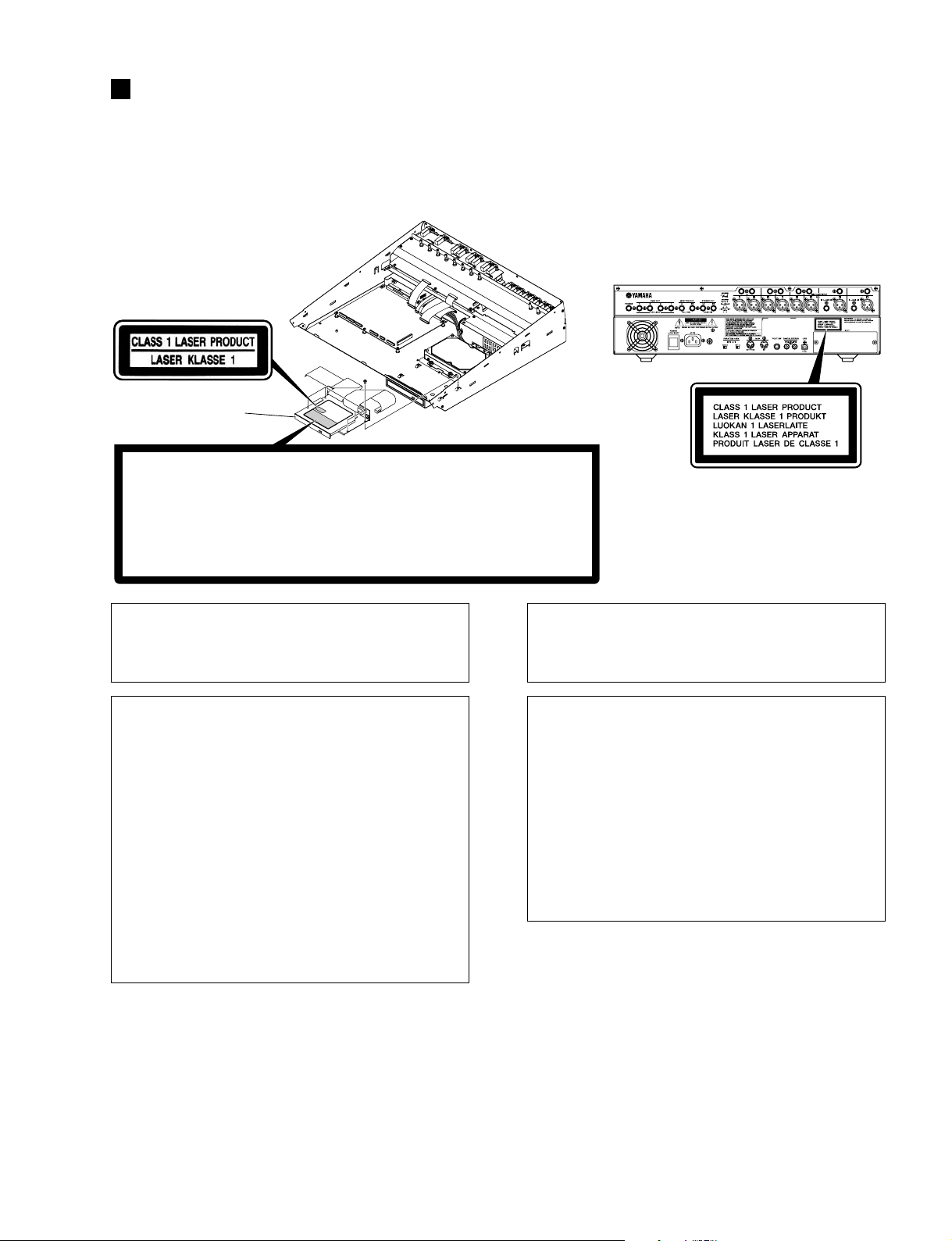
PROTECTION OF EYES FROM LASER BEAM DURING SERVICING
(作業中のレーザー光線からの目の保護)
AW2400
This product employs Class 1 laser. Labels on laser are
located on the upper side of the internal CD-RW drive and
the rear panel of this product.
CD-RW drive
(CD-RWドライブ)
CAUTION
ATTENTION
VORSICHT
ADVARSEL
ADVARSEL
VARNING
VARO
CLASS 3BVISIBLE AND INVISIBLE LASER RADIATION WHEN OPEN. AVOID EXPOSURE TO BEAM.
CLASSE 3B RAYONNEMENT LASER VISIBLE ET INVISIBLE EN CAS D’OUVERTURE.
EXPOSITION DANGEREUSE AU FAISCEAU.
KLASSE 3B SICHTBARE UND UNSICHTBARE LASERSTRAHLUNG, WENN ABDECKUNG GEÖFFNET.
NICHT DEM STRAHL AUSSETZEN.
KLASSE 3B SYNLIG OG USYNLIG LASERSTRÅLING VED ÅBNING. UNDGÅ UDS/ETTELSE FOR STRÅLING.
KLASSE 3B SYNLIG OG USYNLIG LASERSTRÅLING NÅR DEKSEL ÅPNES. UNNGÅ EKSPONERING FOR STRÅLEN.
KLASS 3B SYNLIG OCH OSYNLIG LASERSTRÅLNING NÄR DENNA DEL ÄR ÖPPNAD. STRÅLEN ÄR FARLIG.
KURSSI 3B NÄKYVÄ JA NÄKYMÄTÖN AVATTAESSA OLET ALTTIINA LASERSÄTEILYLLE, ÄLÄ KATSO SÄTEESEN.
Laser properties of the Drive
Laser Class: Class 1 (HHS and IEC 60825-1)
Wavelength: for CD 784 nm
for DVD 662 nm
本製品にはクラス1レーザーが使用されています。レーザー
に関するラベルが内蔵CD-RWドライブの上部、および本製
品のリアパネルにあります。
<Rear view>
CD-RWドライブのレーザー特性
レーザークラス: クラス1(HHS、IEC60825-1)
波長: 784nm(CD)
662nm(DVD)
WARNING Laser Safety
This product contains a laser beam component. This
component may emit in visible, as well as visible radiation,
which may cause eye damage. To protect your eyes and skin
from laser radiation, the following precaution must be used
during servicing of the unit.
1) When testing and / or repairing any component within the
product, keep your eyes and skin more than 30 cm away
from the laser pick-up unit at all time. Do not stare the
laser beam at any time.
2) Do not attempt readjustment, disassemble and repair of
the laser pick-up, unless noted elsewhere in this manual.
3) CAUTION -Use of controls or readjustments or performance
of procedures other than those specified
herein may result in hazardous radiation
exposure.
Do not disassemble the CD-RW drive unit.
VARO!
AVATTAESSA JA SUOJALUKITUS OHITETTAESSA OLET
ALTTIINA NÄKYMÄTTÖMÄLLE LASERSÄTEILYLLE.
ÄLÄ KATSO SÄTEESEEN.
VARNING!
OSYNLIG LASERSTRÅLNING NÄR DENNA DEL ÄR
ÖPPNAD OCH SPÄRREN ÄR URKOPPLAD. BETRAKTA
EJ STRÅLEN.
警告 レーザーの安全性
本製品にはレーザー光線部品が使用されています。この部品
から、目に危険な可視および不可視のレーザー光線が出ます。
レーザー光線から目や皮膚を守るために、本製品における作
業中は次の注意をお守りください。
1) 本製品の検査や修理の際は、常にレーザーピックアップユ
ニットから30cm以上、目と皮膚を離してください。決し
てレーザー光線を見ないでください。
2) 本マニュアルに記載のない限り、レーザーピックアップユ
ニットの調整、分解、修理をしないでください。
3) 注意: 本マニュアルに記載されていない手順で操作する
と、有害な放射を引き起こす可能性があります。
CD-RW ドライブを分解しないでください。
3

AW2400
SPECIFICATIONS
General Specifications
Frequency Response
0+1/-3 dB @20 Hz – 20 kHz
(MIC/LINE INPUT to STEREO OUT, GAIN : max.)
Total Harmonic Distortion
(measured with 20 kHz LPF)
Less than 0.05 % @20 Hz to 20 kHz/+4 dBu
(MIC/LINE INPUT to STEREO OUT, GAIN : min.)
Built-in Hard Disk Drive
40 GB, 3.5" IDE
Maximum Number of Songs
100 Songs
Recording Resolution
16-bit/24-bit
Dynamic Range(measured with IHF-A)
115 dB typ. : DA Converter (STEREO OUT)
109 dB min.: DA Converter (STEREO OUT,
INPUT CH SEL : all off)
110 dB typ. : AD+DA (MIC/LINE INPUT to STEREO OUT)
104 dB min.: AD+DA (MIC/LINE INPUT to STEREO OUT,
GAIN: min.)
AD Converter
24-bit Linear, 128-times Oversampling
DA Converter
24-bit Linear, 128-times Oversampling
Internal Processing
32-bit
Sampling Frequency
Internal : 44.1 kHz, 48 kHz (-6 % – +6 %)
External : 44.1 kHz, 48 kHz (-10 % – +6 %)
Audio Input Section
MIC/LINE INPUT : 8 CH (XLR & phone)
DIGITAL STEREO IN : 2 CH (coaxial stereo x 1)
Mini-YGDAI SLOT : 16 CH
Audio Output Section
MONITOR OUT : 2 CH (stereo x 1)
PHONES : 2 CH (stereo x 1)
STEREO OUT : 2 CH (stereo x 1)
OMNI OUT : 4 CH
DIGITAL STEREO OUT : 2 CH (coaxial stereo x 1)
Mini-YGDAI SLOT : 16 CH
Audio Insert I/O Section
INSERT I/O : 2 CH
Mixer Input Section (Total 48 CH)
MIC/LINE INPUT : 16 CH
Internal Effect Return : 8 CH (stereo x 4)
Track : 24 CH
Maximum Number of Simultaneous Recording/
Playback T racks
16 Recording Tracks/24 Playback Tracks (16-bit)
8 Recording Tracks/12 Playback Tracks (24-bit)
Number of Tracks
208 Tracks
(24 Tracks + Stereo Tracks) x 8 Virtual
Faders
100 mm x 13 (motorized)
Display
320 x 240 dot LCD (with contrast control)
MIDI
MTC (Master/Slave), MIDI Clock (Master),
MMC (Master/Slave), Program Change,
Control Change
Memory
Scene Memory, EQ Library, Compressor Librar y,
Gate Library, Effect Library, Channel Library
Power Consumption
85 W
Dimensions (W x H x D)
533 x 153 x 503 mm
Net Weight
11.5 kg
Operating Temperature
5–35 :
Optional Accessories
Foot switch Yamaha FC5
Internal Effect Section
4 Built-in Multi-Effect Processors
Master Section (Total 16 Bus)
BUS : 4 CH (stereo x 2)
AUX : 4 CH
STEREO : 2 CH (stereo x 1)
SOLO : 2 CH (stereo x 1)
EFFECT : 4 CH
4

Mixer Section
• Input/Output
MIC/LINE INPUT 1-8 (balanced XLR & phone)
Phantom Power Supply : +48 ± 3V
Input Impedance : 3 kΩ
Nominal Input Level : -46 dBu to + 4 dBu
Minimum Input Level : -56 dBu
Maximum Input Leve : +24 dBu
INSERT I/O 1, 2 (unbalanced phone)
Input Impedance : 10 kΩ
Nominal Input Level : 0 dBu
Maximum Input Level : +20 dBu
Output Impedance : 600 Ω
Nominal Output Level : 0 dBu
Maximum Output Level : +20 dBu
AW2400
Internal Effect Return Channels
(EFFECT RETURN 1–4 (stereo))
Equalizer (4-Band PEQ), Pan,
Bus Assign (STEREO, AUX 1–4)
Master Channels
STEREO L, R : Attenuation,
Equalizer (4-Band PEQ),
Compressor, Balance
BUS 1 L/R, 2 L/R : Attenuation, Equalizer (4-Band PEQ),
Compressor, Balance
AUX 1-4 : Attenuation, Equalizer (4-Band PEQ),
Compressor, Balance
EFF 1-4 : Compressor
STEREO OUT L, R (balanced phone)
Output Impedance : 75 Ω
Nominal Load Impedance : 600 Ω
Nominal Output Level : +4 dBu
Maximum Output Level : +24 dBu
MONITOR OUT L, R (balanced phone)
Output Impedance : 75 Ω
Nominal Load Impedance : 600 Ω
Nominal Output Level : +4 dBu
Maximum Output Level : +24 dBu
OMNI OUT 1-4 (unbalanced phone)
Output Impedance : 150 Ω
Nominal Load Impedance : 10 kΩ
Nominal Output Level : +0 dBu
Maximum Output Level : +20 dBu
PHONES (unbalanced TRS phone)
Load Impedance : 8–40 Ω
Maximum Output Level : 25 mW (8 Ω load)
75 mW (40 Ω load)
DIGITAL STEREO IN/OUT (coaxial)
Mini-YGDAI Cards
MY8-AT, MY8-TD, MY8-AE, MY4-AD, MY8-AD,
MY4-DA, MY16-AT, MY16-TD, MY16-AE, MY8-AE96,
MY8-AE96S, MY8-AD24, MY8-AD96, MY8-DA96,
MY16-mLAN, Y96K
* 0 dBu = 0.775 Vrms
Recorder Section
Overview
Recording Resolution : 16-bit/24-bit
Sampling Frequency : 44.1 kHz/48 kHz
Edit Functions
Song Edit : OPTIMIZE, DELETE, COPY, IMPORT
Track Edit : ERASE, DELETE, INSERT, COPY, MOVE,
EXCHANGE, TIME COMP/EXPAND ,
PITCH CHANGE, IMPORT CD AUDIO,
IMPORT CD WAV, IMPORT USB WAV,
IMPORT TRACK, EXPORT
Other Functions
Locate point/Marker
Locate : RTZ, A/B, LAST REC IN/OUT,
Quick Locate 1–9
MARK : 1–99
Punch-In/Out : Manual, Auto
Pitch Fix
CD-RW Drive
Data Backup, Audio CD Burning and Playback,
Audio CD Import, WAV File Import
External Control
MIDI IN : 5-pin DIN
MIDI OUT/THRU : 5-pin DIN
FOOT SW : phone
USB : USB 2.0
• Digital Mixing Functions
Input Channels (INPUT 1–16)
Phase (Normal/Reverse), Gate, Compressor,
Attenuation, Equalizer (4-Band PEQ), Pan,
Bus Assign (STEREO, SOLO, BUS 1–2, AUX 1–4, EFF 1–4)
Track Channels (TRACK 1–24)
Attenuation, Phase (Normal/Reverse),
Equalizer (4-Band PEQ), Compressor, Pan,
Bus Assign (STEREO, BUS 1–2, AUX 1–4, EFF 1–4)
Inclued Items
· The AW2400
· Power cord
· Owner's manual
· CD-ROM
5

AW2400
総合仕様
一般仕様
周波数特性
0+1/−3dB@20Hz〜20kHz(MIC/LINEINPUTto
STEREOOUT,GAIN:最大)
全高調波歪(20kHzLPF)
0.05%以下@20Hz〜20kHz/+4dBu(MIC/LINE
INPUTtoSTEREOOUT,GAIN:最小)
ダイナミックレンジ(IHF-A)
115dBtyp. : DAコンバーター(STEREOOUT)
109dBmin. : DAコンバーター(STEREOOUT,INPUT
CHSEL:すべてオフ)
110dBtyp. : AD+DA(MIC/LINEINPUTtoSTEREOOUT)
104dBmin. : AD+DA(MIC/LINEINPUTto
STEREOOUT,GAIN:最小)
ADコンバーター
24ビットリニア,128倍オーバーサンプリング
DAコンバーター
24ビットリニア,128倍オーバーサンプリング
内部処理
32ビット
サンプリング周波数
内部:44.1kHz,48kHz(−6%〜+6%)
外部:44.1kHz,48kHz(−10%〜+6%)
オーディオ入力部
MIC/LINEINPUT : 8チャンネル
(XLR&フォーン)
DIGITALSTEREOIN : 2チャンネル
(コアキシャル,ステレオ×1)
Mini-YGDAISLOT : 16チャンネル
オーディオ出力部
MONITOROUT : 2チャンネル(ステレオ×1)
PHONES : 2チャンネル(ステレオ×1)
STEREOOUT : 2 チャンネル(ステレオ×1)
OMNIOUT : 4チャンネル
DIGITALSTEREOOUT : 2チャンネル
(コアキシャル,ステレオ×1)
Mini-YGDAISLOT : 16チャンネル
オーディオインサート I/O 部
INSERTI/O : 2チャンネル
ミキサー入力部(合計 48 チャンネル)
MIC/LINEINPUT : 16チャンネル
内部エフェクトリターン : 8チャンネル(ステレオ×4)
トラック : 24チャンネル
内蔵エフェクト部
内蔵マルチエフェクト×4基
マスター部(合計 16 バス)
BUS :4チャンネル(ステレオ×2)
AUX :4チャンネル
STEREO :2チャンネル(ステレオ×1)
SOLO :2チャンネル(ステレオ×1)
EFFECT :4チャンネル
内蔵ハードディスクドライブ
40GB,3.5インチIDE
最大ソング数
100ソング
量子化ビット数
16ビット/24ビット
同時録音 / 再生最大トラック数
16トラック録音/24トラック再生(16ビット)
8トラック録音/12トラック再生(24ビット)
トラック数
208トラック
(24トラック+ステレオトラック)×8バーチャルトラック
フェーダー
100mm×13(モーターフェーダー)
ディスプレイ
320×240ドットLCD(コントラスト調整付き)
MIDI
MTC(Master/Slave),MIDIClock(Master),
MMC(Master/Slave),ProgramChange,
ControlChange
メモリー
シーンメモリー,EQライブラリー,
コンプレッサーライブラリー,ゲートライブラリー,
エフェクトライブラリー,チャンネルライブラリー
消費電力
85W
最大外形寸法(W× H× D)
533×153×503mm
質量
11.5kg
動作環境温度
5〜35℃
オプション
フットスイッチFC5
6

AW2400
ミキサー部
• 入出力
MIC/LINEINPUT1 〜 8(バランス型XLR& フォーン)
ファンタム電源供給 : +48±3V
入力インピーダンス : 3kΩ
定格入力レベル :
最小入力レベル :
最大入力レベル :
−46dBu〜+4dBu
−56dBu
+24dBu
INSERTI/O1,2(アンバランス型フォーン)
入力インピーダンス : 10kΩ
定格入力レベル : 0dBu
最大入力レベル :
出力インピーダンス : 600Ω
定格出力レベル : 0dBu
最大出力レベル : +20dBu
+20dBu
STEREOOUTL,R(バランス型フォーン)
出力インピーダンス : 75Ω
定格負荷インピーダンス : 600Ω
定格出力レベル : +4dBu
最大出力レベル : +24dBu
MONITOROUTL,R(バランス型フォーン)
出力インピーダンス : 75Ω
定格負荷インピーダンス : 600Ω
定格出力レベル : +4dBu
最大出力レベル : +24dBu
OMNIOUT1 〜 4(アンバランス型フォーン)
出力インピーダンス : 150Ω
定格負荷インピーダンス : 10kΩ
定格出力レベル : +0dBu
最大出力レベル : +20dBu
PHONES(アンバランス型 TRS フォーン)
負荷インピーダンス : 8〜40Ω
最大出力レベル : 25mW(8Ω負荷)
75mW(40Ω負荷)
DIGITALSTEREOIN/OUT(コアキシャル)
Mini-YGDAI カード
MY8-AT,MY8-TD,MY8-AE,MY4-AD,MY8-AD,
MY4-DA,MY16-AT,MY16-TD,MY16-AE,
MY8-AE96,MY8-AE96S,MY8-AD24,MY8-AD96,
MY8-DA96,MY16-mLAN,Y96K
*0dBu=0.775Vrms
• デジタルミキサー
インプットチャンネル(INPUT1 〜 16)
フェーズ(Normal/Reverse),ゲート,コンプレッサー,
アッテネーター,イコライザー(4バンドPEQ),パン,
バスアサイン(STEREO,SOLO,BUS1〜2,AUX1〜4,
EFF1〜4)
トラックチャンネル(TRACK1 〜 24)
アッテネーター,フェーズ(Normal/Reverse),
イコライザー(4バンドPEQ),コンプレッサー,パン,
バスアサイン(STEREO,BUS1〜2,AUX1〜4,EFF1〜4)
内蔵エフェクトリターンチャンネル
(EFFECTRETURN1〜 4(ステレオ))
イコライザー(4バンドPEQ),パン,
バスアサイン(STEREO,AUX1〜4)
マスター部
STEREOL,R : アッテネーター,
イコライザー(4バンドPEQ),
コンプレッサー,バランス
BUS1L/R,2L/R : アッテネーター,
イコライザー(4バンドPEQ),
コンプレッサー,バランス
AUX1〜4 : アッテネーター,
イコライザー(4バンドPEQ),
コンプレッサー,バランス
EFF1〜4 : コンプレッサー
レコーダー部
概要
量子化ビット数 : 16ビット/24ビット
サンプリング周波数 : 44.1kHz/48kHz
編集機能
ソング編集 : OPTIMIZE,DELETE,COPY,IMPORT
トラック編集 : ERASE,DELETE,INSERT,COPY,
MOVE,EXCHANGE,
TIMECOMP/EXPAND,
PITCHCHANGE,IMPORTCDAUDIO,
IMPORTCDWAV,IMPORTUSBWAV,
IMPORTTRACK,EXPORT
その他の機能
ロケート/マーカー
ロケート : RTZ,A/B,LASTRECIN/OUT,
クイックロケート1〜9
マーカー : 1〜99
パンチイン/アウト : マニュアル,オート
ピッチフィックス
CD-RW ドライブ
データバックアップ,オーディオCD作成/再生,
オーディオCDインポート,WAVファイルインポート
●外部コントロール
MIDIIN : 5ピンDIN
MIDIOUT/THRU : 5ピンDIN
FOOTSW : フォーン
USB : USB2.0
同梱品
・AW2400本体 :1台
・電源コード :1本
・取扱説明書 :1冊
・保証書 :1枚
・CD-ROM :1枚
7
AW2400
)
)
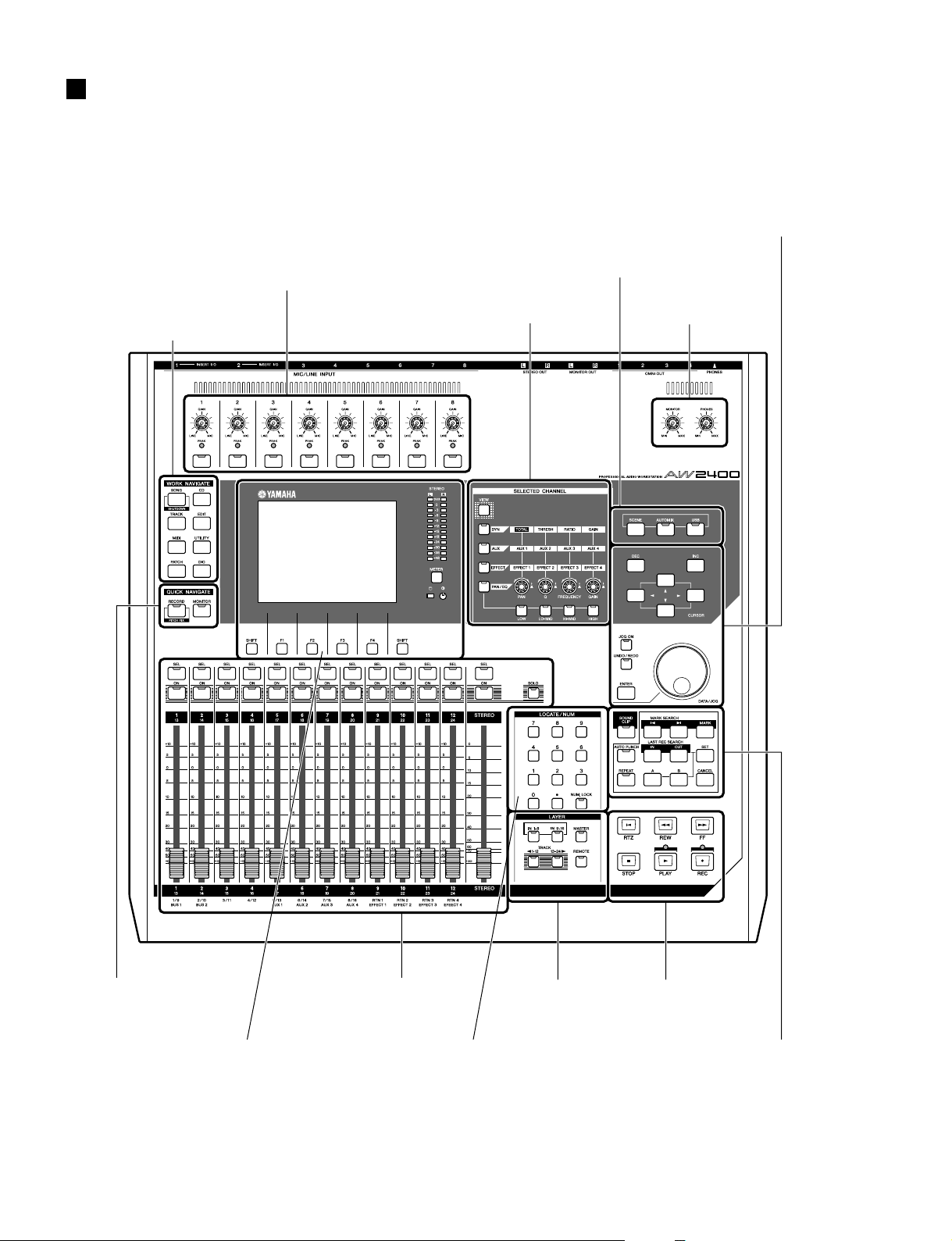
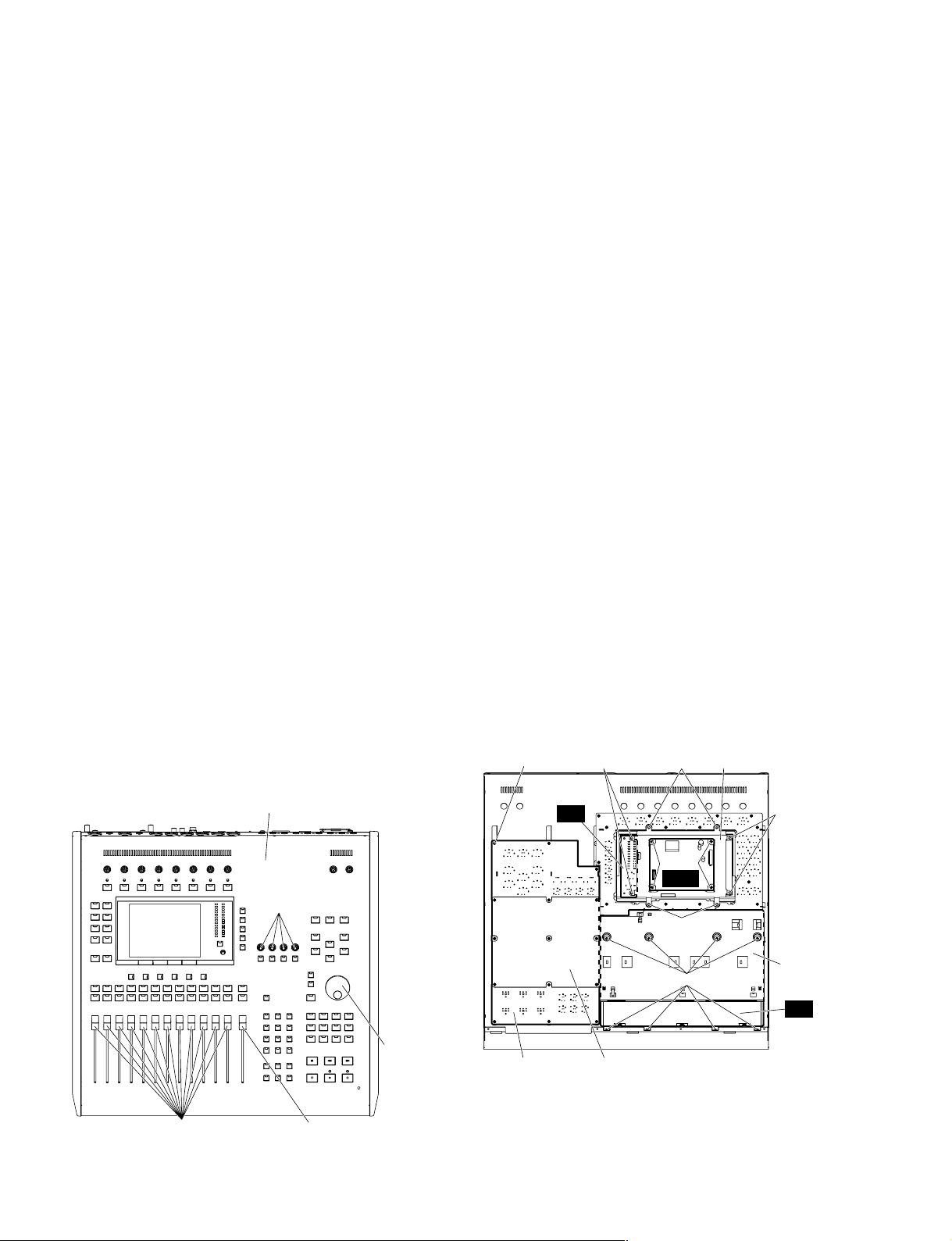
PANEL LAYOUT(パネルレイアウト)
1. T op Panel(トップパネル)
Analog Input Section
(アナログ入出力セクション)
(P. 10)
Work Navigate Section
(ワークナビゲートセクション)
(P. 10)
Scene/Automix/USB Section
(シーン/オートミックス/
USBセクション)
(P. 13)
Selected Channel Section
(セレクテッドチャンネルセクション)
(P. 13)
Data entry/control Section
(データエントリー/
コントロールセクション
(P. 14)
Monitor Section
(モニターセクション)
(P. 13)
Quick Navigate Section
(クイックナビゲートセクション)
(P. 11)
Display Section
(ディスプレイセクション)
(P. 11)
8
Mixer Section
(ミキサーセクション)
(P. 12)
Locate/Number Section
(ロケート/ナンバーセクション)
(P. 14)
Layer Section
(レイヤーセクション)
(P. 15)
Transport Section
(トランスポートセクション)
(P. 15)
Locate Section
(ロケートセクション
(P. 15)
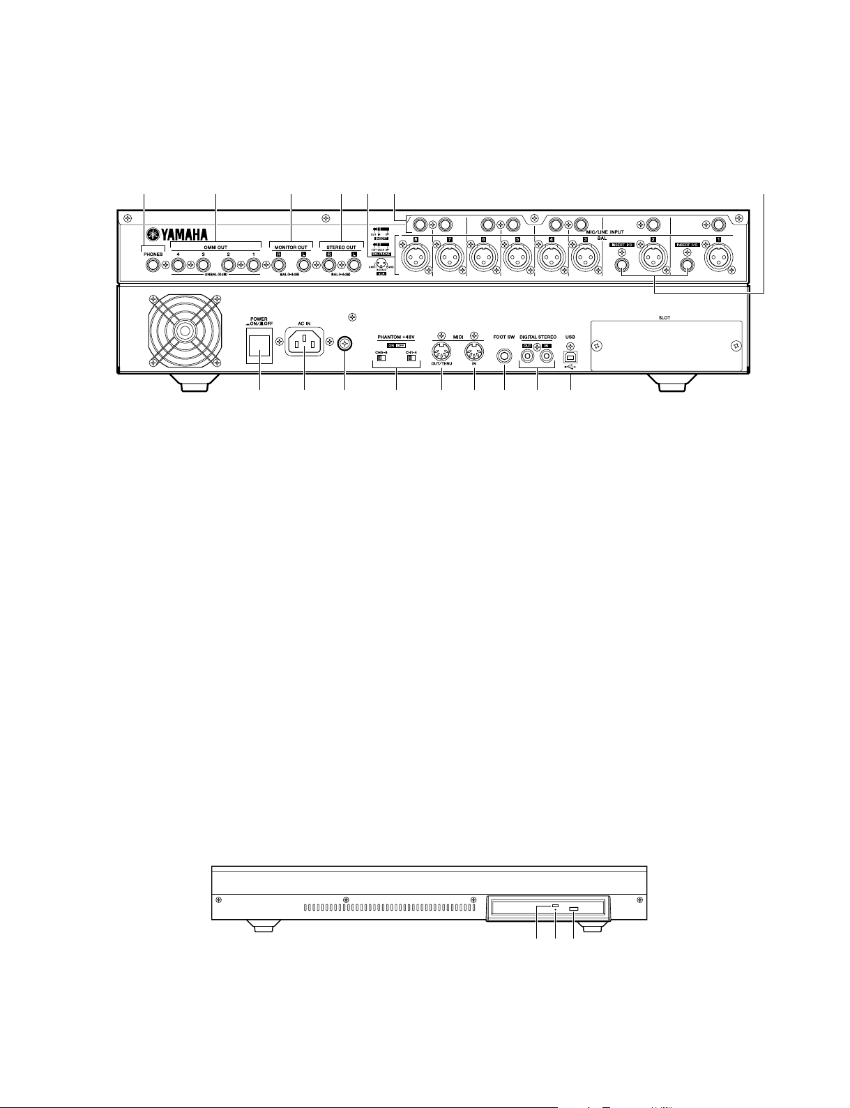
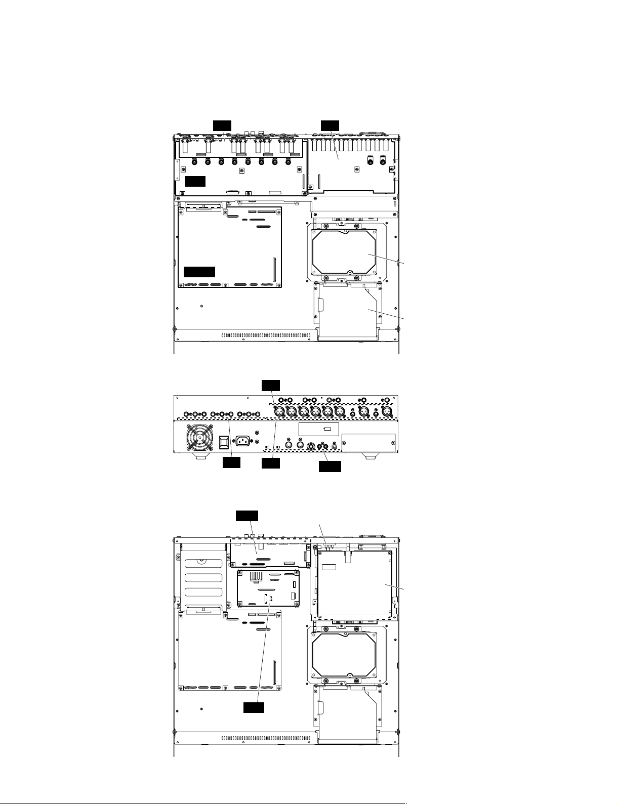
2. Rear Panel(リアパネル)
AW2400
u
q [MIC/LINE INPUT] jacks 1-8 (XLR)
w [MIC/LINE INPUT] jacks 1-8 (TRS phone)
e [INSERT I/O] jacks 1-2
r [STEREO OUT] jacks
t [MONITOR OUT] jacks
y [OMNI OUT] jacks 1-4
u [PHONES] jack
i [POWER] switch
o [AC IN] connector
!0 Ground Screw
!1 PHANTOM +48V [CH1-4] and [CH5-8] switches
!2 [MIDI IN] connector
!3 [MIDI OUT/THRU] connector
!4 FOOT SW jack
!5 [DIGITAL STEREO IN/OUT] connectors
!6 USB connector
!7 SLOT
ytrqw e
io
!0 !1 !2 !3 !4 !5 !6
!7
q [MIC/LINEINPUT(XLR)]端子1〜 8
w [MIC/LINEINPUT(TRSフォーン)]端子1〜 8
e [INSERTI/O]端子1〜 2
r [STEREOOUT]端子
t [MONITOROUT]端子
y [OMNIOUT]端子1〜 4
u [PHONES]端子
i [POWER]スイッチ
o0 [ACIN]端子
!0 アースねじ
!1 [PHANTOM+48V]スイッチ
!2 [MIDIIN]端子
!3 [MIDIOUT/THRU]端子
!4 FOOTSW端子
!5 DIGITALSTEREOIN/OUT端子
!6 USB端子
!7 SLOT
([CH1-4]スイッチ、[CH5-8]スイッチ)
3. Front Panel(フロントパネル)
• CD-R/RW Drive(CD-R/RWドライブ)
q Eject switch
w Eject hole
e Access indicator
qwe
q イジェクトスイッチ
w イジェクトホール
e アクセスランプ
9
AW2400
4. Top Panel Details(トップパネル詳細)
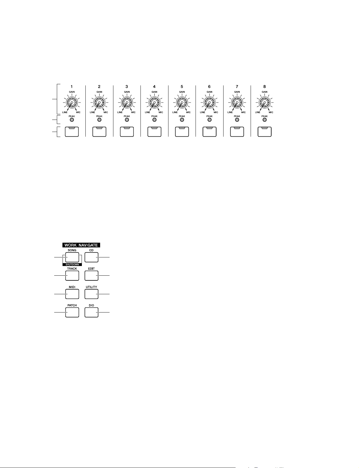
4-1 Analog Input section(アナログ入力セクション)
q
w
e
q [GAIN] knobs 1-8
w [PEAK] Indicators
e [INPUT SEL] keys 1-8
q [GAIN]ノブ1 〜8
w [PEAK]インジケーター
e [INPUTSEL]キー1 〜8
4-2 Work Navigate section(ワークナビゲートセクション)
q
e
t
u
w
r
y
i
q [SONG] key
w [CD] key
e [TRACK] key
r [EDIT] key
t [MIDI] key
y [UTILITY] key
u [PATCH] key
i [DIO] key
q [SONG]キー
w [CD]キー
e [TRACK]キー
r [EDIT]キー
t [MIDI]キー
y [UTILITY]キー
u [PATCH]キー
i [DIO]キー
10
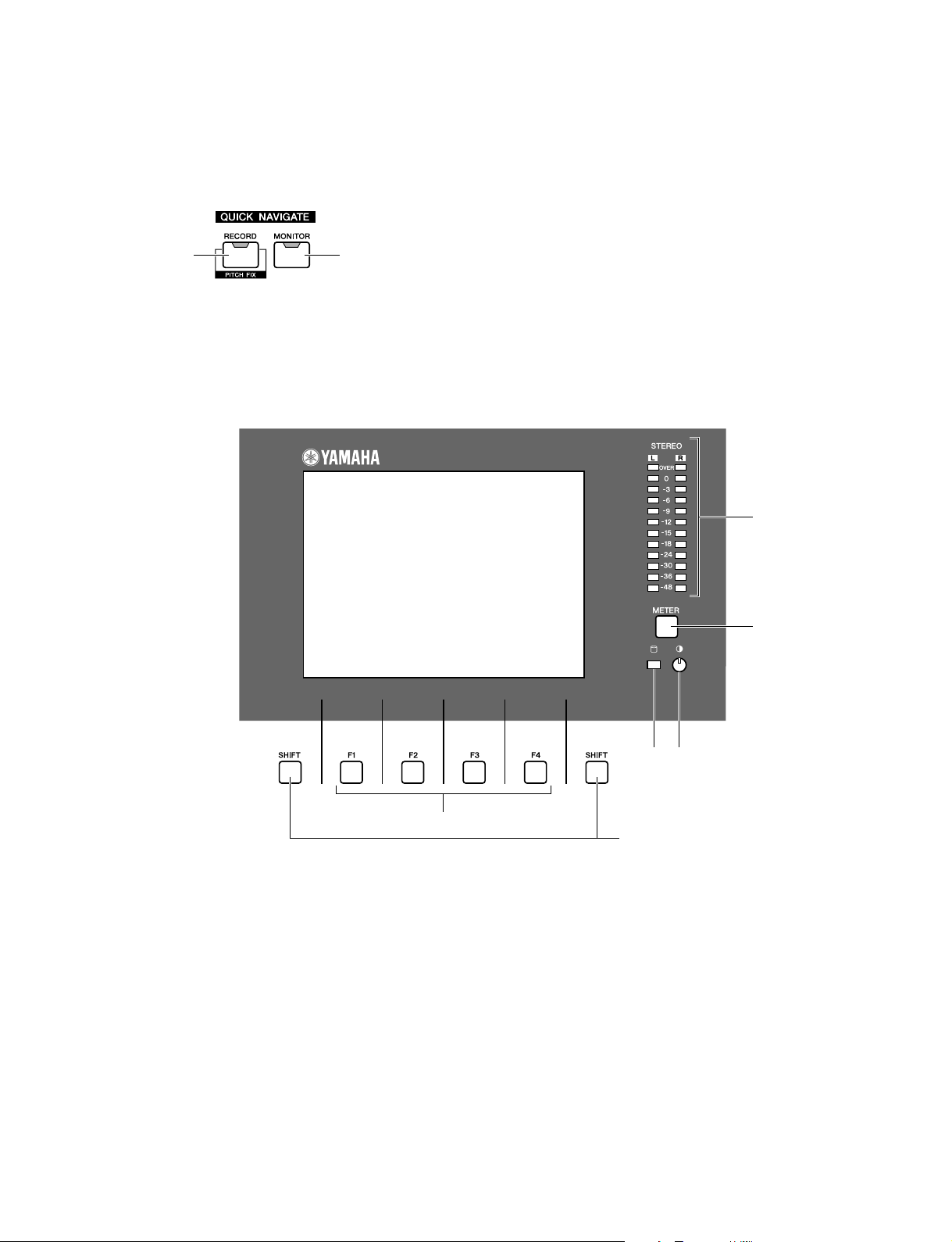
4-3 Quick Navigate section(クイックナビゲートセクション)
AW2400
q
w
4-4 Display section(ディスプレイセクション)
q1
q [RECORD] key
w [MONITOR] key
q [RECORD]キー
w [MONITOR]キー
w
e
q Display
w Stereo Meters
e [METER] key
r Contrast
t Access indicator
y [F1] - [F4] keys
u [SHIFT] key
rt
y
u
q ディスプレイ
w ステレオメーター
e [METER]キー
r コントラスト
t アクセスインジケーター
y [F1]〜[F4]キー
u [SHIFT]キー
11
AW2400
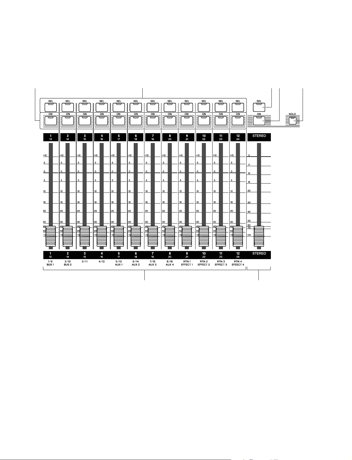
4-5 Mixer section(ミキサーセクション)
qe wr u
12
q [SEL] keys 1-12
w [STEREO SEL] key
e [ON] keys 1-12
r [STEREO ON] key
t Faders 1-12
y [STEREO] fader
u [SOLO] key
ty
q [SEL]キー1 〜12
w [STEREOSEL]キー
e [ON]キー1 〜12
r [STEREOON]キー
t フェーダー1 〜12
y [STEREO]フェーダー
u [SOLO]キー
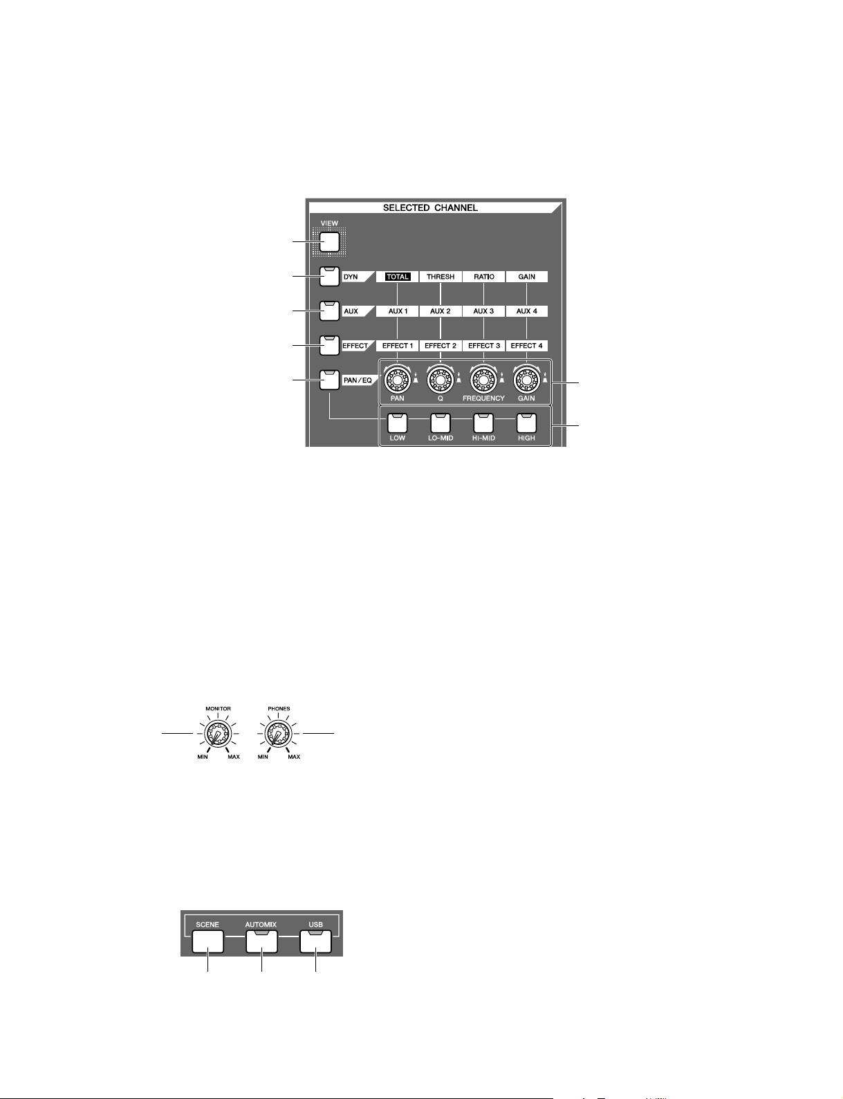
4-6 Selected Channel section(セレクテッドチャンネルセクション)
q
w
e
r
AW2400
t
q [VIEW] key
w [DYN] key
e [AUX] key
r [EFFECT] key
t [PAN/EQ] key
y SELECTED CHANNEL knobs 1-4
u [LOW], [LO-MID], [HI-MID], and [HIGH] keys
4-7 Monitor section(モニターセクション)
qw
y
u
q [VIEW]キー
w [DYN]キー
e [AUX]キー
r [EFFECT]キー
t [PAN/EQ]キー
y セレクテッドチャンネルノブ1〜 4
u [LOW]キー、[LO-MID]キー、[HI-MID]キー、[HIGH]キー
q [MONITOR] knob
w [PHONES] knob
q [MONITOR]ノブ
w [PHONES]ノブ
4-8 Scene/Automix/USB section(シーン/ オートミックス/USB セクション)
q [SCENE] key
w [AUTOMIX] key
e [USB] key
qwe
q [SCENE]キー
w [AUTOMIX]キー
e [USB]キー
13
AW2400
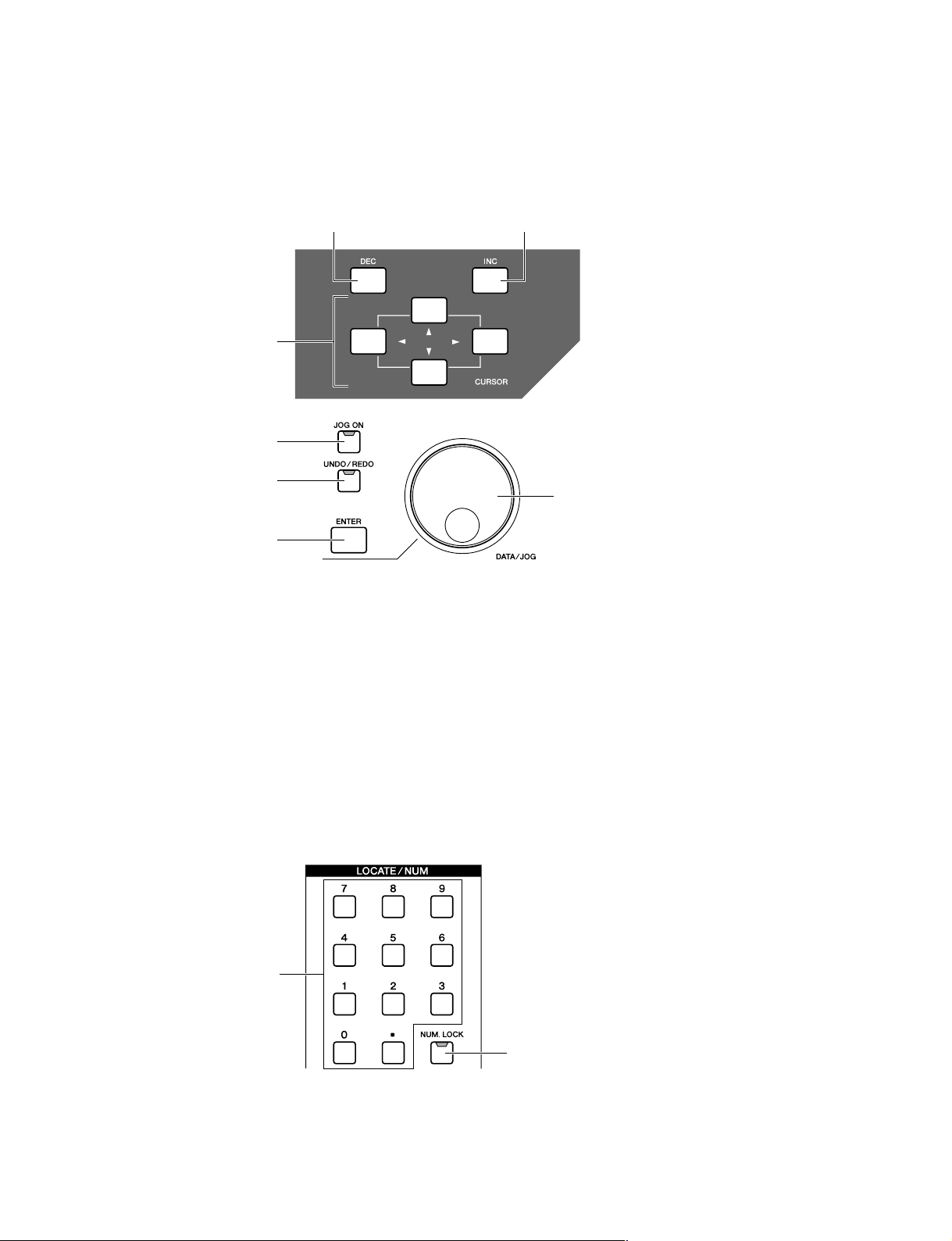
4-9 Data entry/control section(データエントリー /コントロールセクション)
qw
e
r
t
y
q [INC] key
w [DEC] key
e [Cursor] keys ([▲] / [▼] / [t] / [s] keys)
r [JOG ON] key
t [UNDO/REDO] key
y [ENTER] key
u [DATA/JOG] dial
q [INC]キー
w [DEC]キー
e カーソルキー([▲]/[▼]/[t]/[s]キー)
r [JOGON]キー
t [UNDO/REDO]キー
y [ENTER]キー
u [DATA/JOG]ダイアル
4-10 Locate/Number section(ロケート /ナンバーセクション)
u
14
q
q [LOCATE] keys
w [NUM.LOCK] key
w
q [LOCATE]キー
w [NUM.LOCK]キー
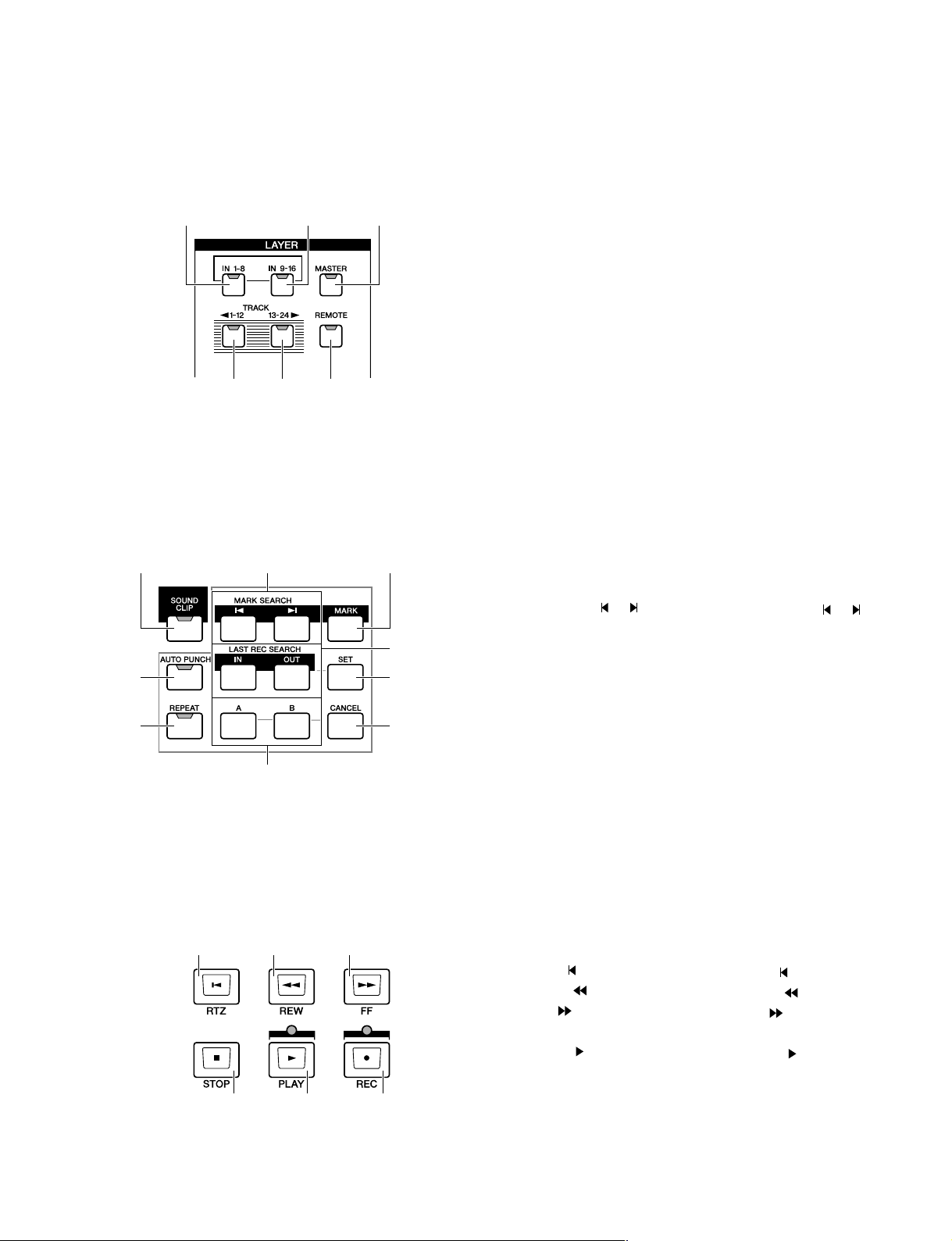
4-11 Layer section(レイヤーセクション)
qwe
AW2400
rty
4-12 Locate section(ロケートセクション)
qwe
t
r
u
y
o
i
q [IN 1-8] key
w [IN 9-16] key
e [MASTER] key
r [TRACK 1-12] key
t [TRACK 13-24] key
y [REMOTE] key
q [SOUND CLIP] key
w MARK SEARCH [ ] / [ ] keys
e [MARK] key
r [AUTO PUNCH] key
t [IN] / [OUT] keys
y [SET] key
u [REPEAT] key
i [A] / [B] keys
o [CANCEL] key
q [IN1-8]キー
w [IN9-16]キー
e [MASTER]キー
r [TRACK1-12]キー
t [TRACK13-24]キー
y [REMOTE]キー
q [SOUNDCLIP]キー
w MARKSEARCH[
e [MARK]キー
r [AUTOPUNCH]キー
t [IN]/[OUT]キー
y [SET]キー
u [REPEAT]キー
i [A]/[B]キー
o [CANCEL]キー
]/[ ]キー
4-13 T ransport section(トランスポートセクション)
qwe
rty
q RTZ [ ] key
w REW [ ] key
e FF [ ] key
r STOP [■] key
t PLAY [
y REC [●] key
] key
q RTZ[
w REW[
e FF[ ]キー
r STOP[■]キー
t PLAY[
y REC[●]キー
]キー
]キー
]キー
15
AW2400
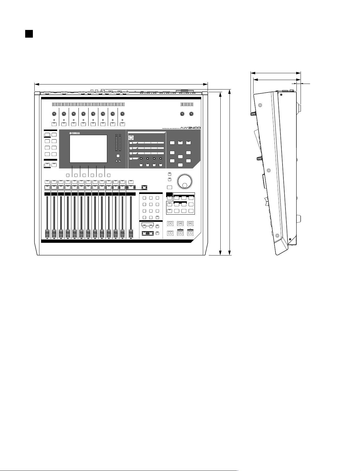
DIMENSIONS(寸法図)
533
497
503
153
145
13
Unit : mm
(単位)
16
AW2400
PN2
PN1
LCD
FD
ML
<Bottom view>
Sheet PN2 assembly
(シートPN2Assy)
LCD
(液晶ディスプレイ)
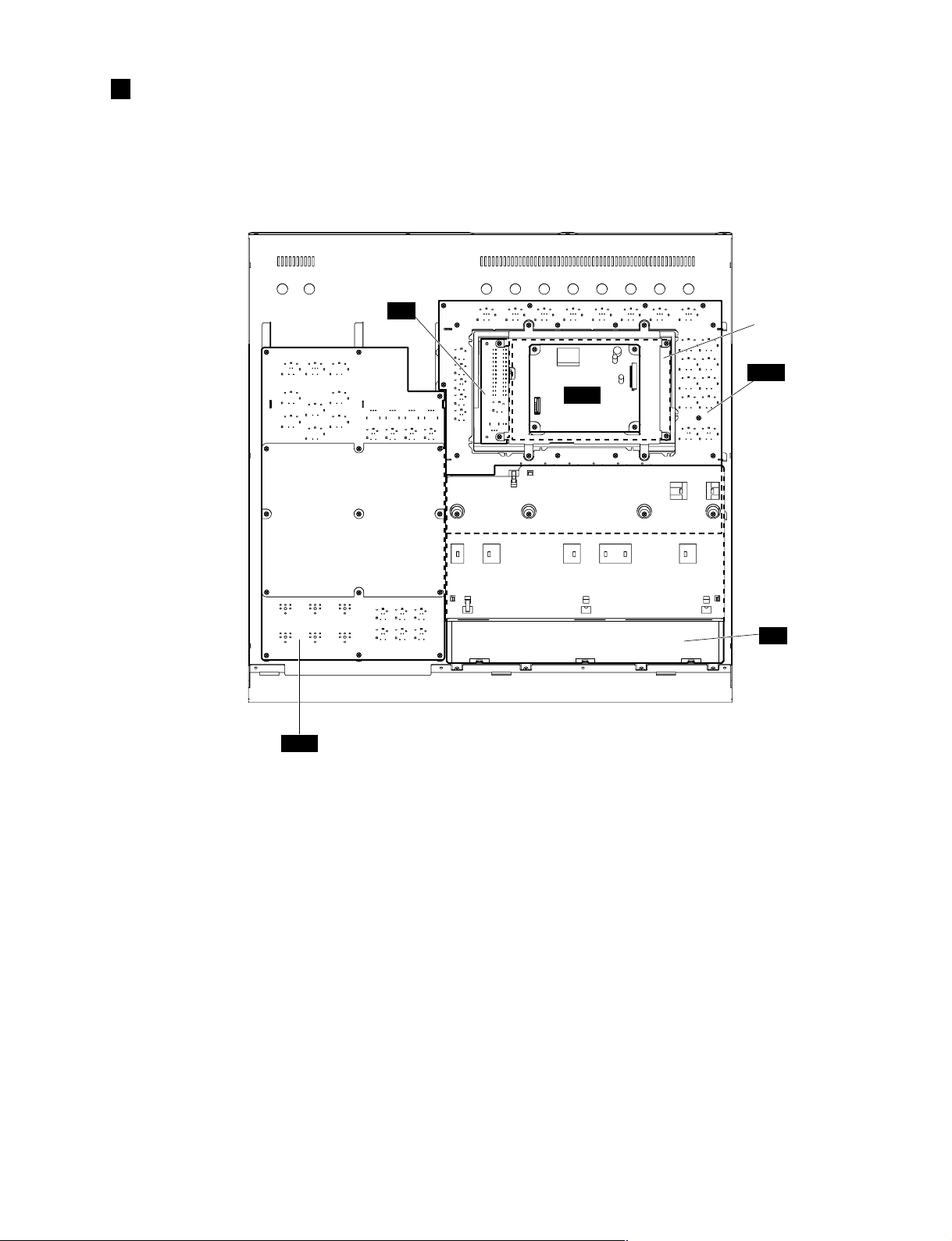
CIRCUIT BOARD LAYOUT
• T op Parts(トップ部)
(ユニットレイアウト)
17
AW2400
• Bottom Parts(ボトム部)
<Top view>
JK DA
AD
<Rear view>
<Top view>
MAIN
DA
DIO
JK
AD
Hard disk drive assembly
(HDDAssy)
CD drive assembly
(CDドライブAssy)
DIO
AC inlet assembly
(インレットAss'y)
18
Power supply unit
(電源ユニット)
PW
AW2400
DISASSEMBLY PROCEDURE
Precautions(注意事項)
After replacing the FD circuit board, be sure to calibrate
the faders. (See page 63.)
Notes on Flat Cable
Contacts are visible from the back. Pay attention not to
insert and install the cable to the connector inversely.
(Photo 1)
Front Side (Printed Side)
(表面(印刷面))
Photo 1 (写真1)
1. Top Cover (Time required: About 3 minutes)
1-1 Remove the eight (8) knobs (white/black) and the
two (2) knobs (red/black) from the control panel
surface. (Fig.1)
1-2 Remove the six (6) screws marked [1320A]. The
side pad R and side pad L can then be removed.
(Fig.1)
1-3 Remove the ten (10) screws marked [1320B]. The
top cover can then be removed. (Fig.1, 2)
* When installing the top cover, insert the three
(3) claws of the bottom cover in the holes of
the top cover. (Fig.1)
<Rear view>
(分解手順)
FDシートを交換後は、フェーダーのキャリブレーション
を実施してください。(68 ページ参照)
フラットケーブルの注意
接点が裏面から透けて見えます。コネクタにケーブルの
表・裏を逆に差込まないように注意して取り付けてくだ
さい。(写真 1)
Back Side (裏面)
1. トップカバー(所要時間:約3分)
1-1 コントロールパネル面より、ノブ(VR)(白/黒)8個
とノブ(VR)(赤/黒)2個を外します。(図1)
1-2 [1320A]のネジ6本を外して、サイドパッドRとサイ
ドパッドLを外します。(図1)
1-3 [1320B]のネジ10本を外して、トップカバーを外し
ます。(図1、図2)
※ トップカバーを取り付けの際は、ボトムカバーの
ツメ(3箇所)をトップカバーの穴に入れて取り付け
てください。(図1)
[1320B]
<Left side view>
[1320A]
Side pad L
(サイドパッドL)
[1320]: Bind Head Tapping Screw-B(Bタイト+BIND)3.0X8 MFZN2B3 (WE774400)
<Top view>
<Front view>
Knob (White/Black)
(ノブ(VR)(白/黒))
[1320B]
Fig.1 (図1)
Knob (Red/Black)
(ノブ(VR)(赤/黒))
Top cover
(トップカバー)
<Right side view>
[1320A]
Top cover
(トップカバー)
Hole (穴)
Side pad R
(サイドパッドR)
Claw (ツメ)
Bottom cover
(ボトムカバー)
19
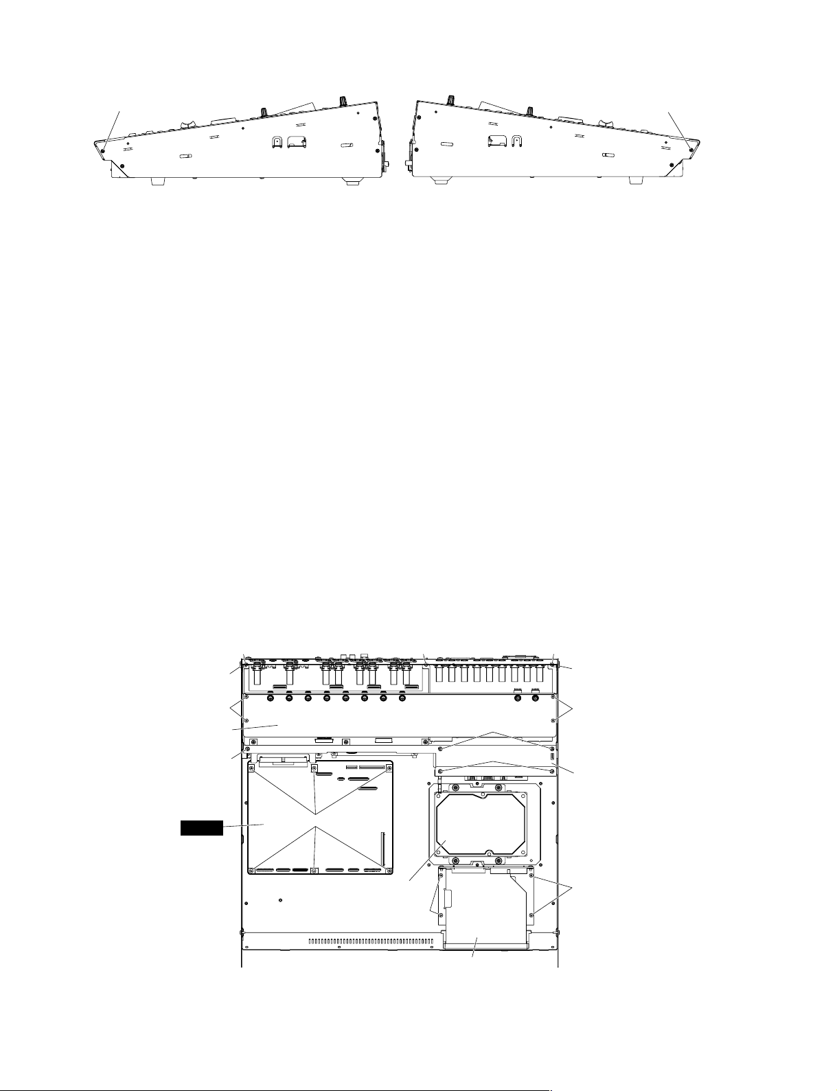
AW2400
[1320B]
<Left side view><Right side view>
[1320B]
[1320B]: Bind Head Tapping Screw-B (Bタイト+BIND)3.0X8 MFZN2B3 (WE774400)
Fig.2 (図2)
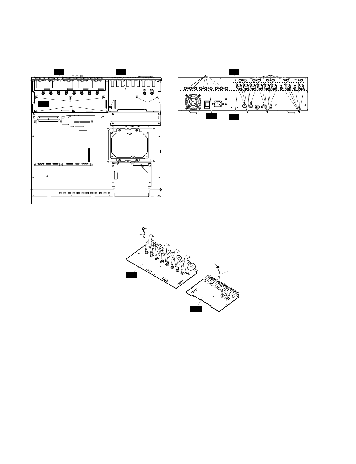
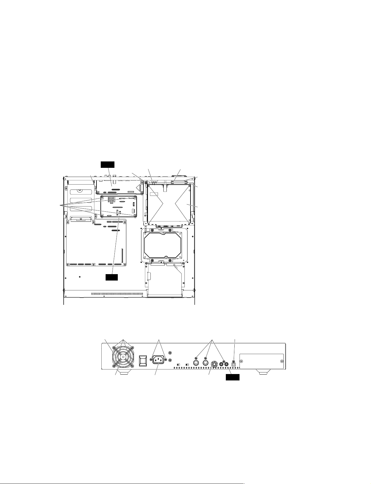
A. Bottom Section Disassembly Procedure
A-1. MAIN Circuit Board
(Time required: About 4 minutes)
A-1-1 Remove the top cover. (See procedure 1)
A-1-2 Remove the six (6) screws marked [400]. The MAIN
circuit board can then be removed. (Fig.3)
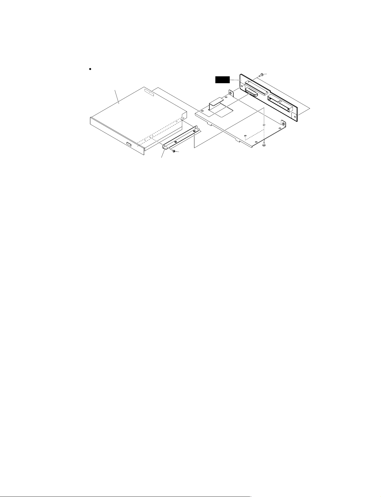
A-2. CD Drive Assembly, IDE Circuit Board,
DVD & CD-R/W drive
(Time required: About 4 minutes)
A-2-1 Remove the top cover. (See procedure 1)
A-2-2 Remove the f our (4) screws mark ed [190]. The CD
drive assembly can then be removed. (Fig.3)
A-2-3 Remove the two (2) screws marked [70]. Then, pull
the IDE circuit board to remove it from the CD drive
assembly. (Fig.4)
A-2-4 Remove the two (2) screws marked [30A]. The
CDRW support and DVD & CD-R/W drive can then
be removed. (Fig.4)
<Top view>
[500B] [500B] [500B]
[1320C]
A. ボトム部の分解
A-1. MAINシート(所要時間:約4分)
A-1-1 トップカバーを外します。(1項参照)
A-1-2 [400]のネジ6本を外して、MAINシートを外しま
す。(図3)
A-2.
A-2-1 トップカバーを外します。(1項参照)
A-2-2 [190]のネジ4本を外して、CDドライブAssyを外し
A-2-3 [70]のネジ2本を外して、IDEシートをCDドライブ
A-2-4 [30A]のネジ2本を外して、サポートCDRWとDVD
CDドライブAss y、IDEシート、DVD&CD-R/W
(所要時間:約4分)
ます。(図3)
Ass yから引っ張って外します。(図4)
&CD-R/Wを外します。(図4)
[1320C]
20
[500A]
ADDA shield plate
(シールドADDA)
[500B]
MAIN
[190]: Bind Head Tapping Screw-S (Sタイト+BIND) 3.0X6 MFZN2W3 (WE877900)
[400]: Bind Head Tapping Screw-B (Bタイト+BIND) 3.0X6 MFZN2W3 (WE936300)
[500]: Bind Head Tapping Screw-B (Bタイト+BIND) 3.0X6 MFZN2W3 (WE936300)
[520]: Bind Head Tapping Screw-B (Bタイト+BIND) 3.0X6 MFZN2W3 (WE936300)
[1320C]: Bind Head Tapping Screw-B (Bタイト+BIND) 3.0X8 MFZN2B3 (WE774400)
[400]
Hard disk drive assembly
(HDD Ass'y)
[190]
CD drive assembly (CDドライブAss'y)
Fig.3 (図3)
[500A]
[500B]
[520]
ADDA holder
(ホルダーADDA)
[190]
AW2400
CD Drive Assembly(CDドライブAss'y)
DVD & CD-R/W drive
(DVD & CD-R/W)
[30A]
CDRW support
(サポートCDRW)
[30A]: Pan Head Screw (小ネジ+PAN) 2.0X2 MFZN2W3 (WE878500)
[70]: Bind Head Tapping Screw-S (Sタイト+BIND) 3.0X6 MFZN2W3 (WE877900)
A-3. JK Circuit Board
(Time required: About 4 minutes)
A-3-1 Remove the top cover. (See procedure 1)
A-3-2 Remove the five (5) screws marked [450A]. The JK
circuit board can then be removed. (Fig.5)
[70]
IDE
Fig.4 (図4)
A-3. JKシート(所要時間:約4分)
A-3-1 トップカバーを外します。(1項参照)
A-3-2 [450A]のネジ5本を外して、JKシートを外します。
(図5)
A-4 AD Circuit Board, DA Circuit Board
A-4-1 Remove the top cover. (See procedure 1)
A-4-2 Remove the four (4) screws marked [500A]. The
ADDA shield plate can then be removed. (Fig.3)
A-4-3 AD Circuit Board
(Time required: About 7 minutes)
A-4-3-1
A-4-4 DA Circuit Board
A-4-4-1
* The knob spacer and gain spacer are not part of
Remove the eighteen (18) screws marked [450B],
and six (6) screws marked [460A]. The AD circuit
board can then be removed. (Fig.5)
(Time required: About 5 minutes)
Remove the six (6) screws marked [450C], and
three (3) screws marked [460B]. The DA circuit
board can then be removed. (Fig.5)
the AD circuit board or DA circuit board. When
replacing the AD circuit board or D A circuit board,
remove the knob spacer and gain spacer from
the AD circuit board or DA circuit board and
install them to the new circuit board. (Fig.6)
A-4. ADシート、DAシート
A-4-1 トップカバーを外します。(1項参照)
A-4-2 [500A]のネジ4本外して、シールドADDAを外しま
す。(図3)
A-4-3 ADシート(所要時間:約7分)
A-4-3-1 [450B]のネジ18本と[460A]のネジ6本を外して、
ADシートを外します。(図5)
A-4-4 DAシート(所要時間:約5分)
A-4-4-1 [450C]のネジ6本と[460B]のネジ 3 本を外して、 DA
シートを外します。(図5)
※ ノブスペーサーとスペーサーG A I Nは、A Dシー
ト、DA シートの構成部品ではありません。A D
シートまたはDA シートを交換する際には、AD
シートまたはDAシートからノブスペーサーとス
ペーサーGAINを取り外して、新しいシートに取り
付けてください。(図6)
21
AW2400
JK DA
AD
[460A]
[460B]
[460B]
<Rear view><Top view>
[450C]
JK
[450A]
Knob spacer
(ノブスペーサー)
AD
Fig.5 (図5)
Gain spacer
(スペーサーGAIN)
DA
[450]: Bonding T apping Screw-B (Bタイト+BOND)
3.0X10 MFZN2B3 (WE878000)
[460]: Bind Head Tapping Screw-S (Sタイト+BIND)
3.0X6 MFZN2W3 (WE877900)
Gain spacer
(スペーサーGAIN)
AD
Knob spacer
(ノブスペーサー)
[450B][450B]
[450B]
A-5. PW Circuit Board
(Time required: About 5 minutes)
A-5-1 Remove the top cover. (See procedure 1)
A-5-2 Remove the six (6) screws marked [500B], two (2)
screws marked [520], and two (2) screws marked
[1320C]. The ADDA holder can then be removed.
(Fig.3)
A-5-3 Remove the four (4) scre ws mark ed [380]. The PW
circuit board can then be removed. (Fig.7)
22
Fig.6 (図6)
DA
A-5. PWシート(所要時間:約5分)
A-5-1 トップカバーを外します。(1項参照)
A-5-2 [500B]のネジ 6本と[520]の ネジ 2本、 [1320C]のネ ジ
2本を外して、ホルダーADDAを外します。(図3)
A-5-3 [380]のネジ4本を外して、PWシートを外します。
(図7)
AW2400
A-6. DIO Circuit Board
(Time required: About 6 minutes)
A-6-1 Remove the top cover. (See procedure 1)
A-6-2 Remove the ADDA holder. (See procedure A-5-2)
A-6-3 Remove the three (3) screws marked [330], the
hexagonal nut marked [340], the three (3) screws
marked [350], and the screw marked [360]. The DIO
circuit board can then be removed. (Fig.7, 8)
<Top view>
[380]
DIO
AC inlet assembly
(インレットAss'y)
[310][330]
[330]
Fan angle blacket
(ファン金具)
[260]
A-6. DIOシート(所要時間:約6分)
A-6-1 トップカバーを外します。(1項参照)
A-6-2 ホルダーADDAを外します。(A-5-2項参照)
A-6-3 [330]のネジ3本と[340]の特種六角ナット1個、
[350]のネジ3本、[360]のネジ1本を外して、DIO
シートを外します。(図7、図8)
Motor
(DCファンモーター)
Fan angle blacket
(ファン金具)
Power supply unit
(電源ユニット)
PW
<Rear view>
Finger guard
(フィンガーガード)
Motor
(DCファンモーター)
[230]: Pan Head Screw (小ネジ+PAN) SP4.0X25 MFZN2B3 (WE924100)
[300]: Bonding T apping Screw-B (Bタイト+BOND)3.0X10 MFZN2B3 (WE878000)
[340]: Hexagonal Nut (特種六角ナット) (V9475600)
[350]: Bonding T apping Screw-B (Bタイト+BOND)3.0X10 MFZN2B3 (WE878000)
[360]: Bind Head Screw (小ネジ+BIND) 3.0X6 MFZN2B3 (WE878300)
[300]
AC inlet assembly
(インレットAss'y)
Fig.7 (図7)
Fig.8 (図8)
[260]: Bind Head Tapping Screw-B (Bタイト+BIND)
3.0X6 MFZN2W3 (WE936300)
[310]: Bind Head Tapping Screw-S (Sタイト+BIND)
4.0X8 MFZN2W3 (WE941800)
[330]: Bind Head Tapping Screw-S (Sタイト+BIND)
3.0X6 MFZN2W3 (WE877900)
[380]: Bind Head Tapping Screw-S (Sタイト+BIND)
3.0X6 MFZN2W3 (WE877900)
[350][230] [360]
[340]
DIO
23
AW2400
A-7. Power Supply Unit
(Time required: About 5 minutes)
A-7-1 Remove the top cover. (See procedure 1)
A-7-2 Remove the ADDA holder. (See procedure A-5-2)
A-7-3 Set the AC cover in a horizontal position. (Photo 2)
A-7-4 Remove the four (4) screws marked [260]. The
power supply unit can then be removed. (Fig.7)
* The power switch knob and rod are not part of
the power supply unit. When replacing the
power supply unit, remove the power switch
knob and rod from the power supply unit and
install them to the new power supply unit.
(Photo 3)
* When installing the power supply unit, be sure
to set the AC cover just as it was.
AC cover
(カバーAC)
Power supply unit
(電源ユニット)
A-7. 電源ユニット(所要時間:約5分)
A-7-1 トップカバーを外します。(1項参照)
A-7-2 ホルダーADDAを外します。(A-5-2項参照)
A-7-3 カバーACを縦にします。(写真2)
A-7-4 [260]のネジ4本を外して、電源ユニットを外しま
す。(図7)
※ PSWノブとロッドは、電源ユニットの構成部品で
はありません。電源ユニットを交換する際には、
電源ユニットからPSWノブとロッドを取り外し
て、新しい電源ユニットに取り付けてください。
(写真3)
※ 電源ユニットを組み立てる際には、カバーACを必
ず元通りにしてください。
Power switch knob (PSWノブ)
Power supply unit
(電源ユニット)
Rod
(ロッド)
Photo 2 (写真2)
A-8. Motor (Time required: About 6 minutes)
A-8-1 Remove the top cover. (See procedure 1)
A-8-2 Remove the ADDA holder. (See procedure A-5-2)
A-8-3 Remove the power supply unit.
(See procedure A-7-4)
A-8-4 Remove the insulation sheet. (Photo 4)
A-8-5 Remove the four (4) scre ws marked [230]. The finger
guard, two (2) fan angle brackets and motor can
then be removed. (Fig.7, 8, Photo 4)
* When replacing the motor , install the insulation
sheet just as it was before removal.
* When installing the connector assembly from
the motor, pass the connector assembly in the
hole of the insulation sheet from bottom up.
(Photo 4)
Photo 3 (写真3)
A-8. DCファンモーター(所要時間:約6分)
A-8-1 トップカバーを外します。(1項参照)
A-8-2 ホルダーADDAを外します。(A-5-2項参照)
A-8-3 電源ユニットを外します。(A-7-4項参照)
A-8-4 絶縁シートを外します。(写真4)
A-8-5 [230]のネジ4本を外して、フィンガーガードと
ファン金具2個、DCファンモーターを外します。
(図7、図8、写真4)
※ DCファンモーターを交換する際には、絶縁シート
を必ず元通りに取り付けてください。
※ DCファンモーターからの束線は絶縁シートの穴を
下から上に通して取り付けてください。(写真4)
Motor (DCファンモーター)
Fan angle blacket
Fan angle blacket
ファン金具)
ファン金具
(
24
Insulation sheet
(絶縁シート)
Hole (穴)
Connector assembly (束線)
Photo 4 (写真4)
AW2400
A-9. AC Inlet Assembly
(Time required: About 5 minutes)
A-9-1 Remove the top cover. (See procedure 1)
A-9-2 Remove the ADDA holder. (See procedure A-5-2)
A-9-3 Remove the two (2) screws marked [300] and the
screw marked [310]. The AC inlet assembly can
then be removed. (Fig.7, 8)
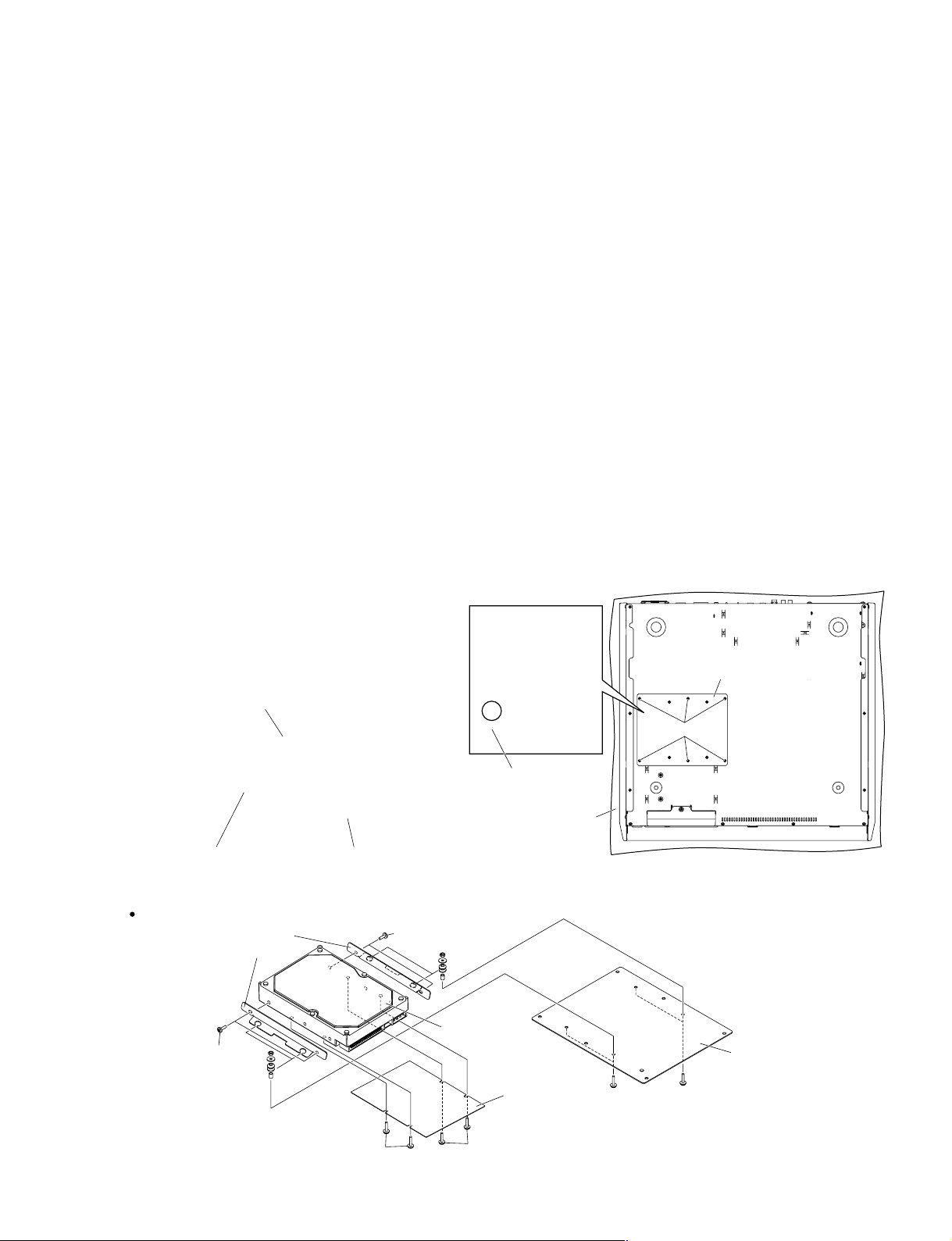
A-10. Hard Disk Drive Assembly, Hard Disk
Drive (Time required: About 2 minutes)
A-10-1 Paying attention not to damage the main unit, place
it upside down on a cloth. (Fig.9)
A-10-2 Remove the six (6) screws marked [170], and lift
the hard disk drive assembly as shown in photo 5.
Remove the terminals of the connector assemblies
at the two (2) connecting parts for the hard disk
drive and remove the hard disk drive assembly.
(Fig.9, Photo 5)
A-10-3 Remove the four (4) screws marked [30B]. The two
(2) HDD supports and HDD cover can then be
removed. (Fig.10)
A-10-4 Remove the four (4) screws marked [16]. The HDD
under cover can then be removed from the hard
disk drive. (Fig.10)
* Insert a minus driver in the portion shown
in the circle "○" to remove the hard disk
drive assembly.
※○の部分にマイナスドライバーを差し込むと
HDDAss yを外すことが出来ます。
A-9. インレットAss y(所要時間:約5分)
A-9-1 トップカバーを外します。(1項参照)
A-9-2 ホルダーADDAを外します。(A-5-2項参照)
A-9-3 [300]のネジ2本と[310]のネジ1本を外して、イン
レットAss yを外します。(図7、図8)
A-10. HDDAss y、HDD(所要時間:約2分)
A-10-1 本体を傷つけないように、布の上に裏返しにして
置きます。(図9)
A-10-2 [170]のネジ6本を外して、写真5のようにHDD
Ass yを持ち上げます。
ハードディスクのコネクター部2 ヶ所から線材
Ass yの端子を抜いて、HDDAss yを外します。
(図9、写真5)
A-10-3 [30B]のネジ4本を外して、サポートHDD2個と
HDDフタを外します。(図10)
A-10-4 [16]のネジ4本を外して、HDDからHDDアンダー
カバーを外します。(図10)
<Bottom view>
Hard disk drive assembly
(HDD Ass'y)
Hard disk drive assembly (HDD Ass'y)
Connector assembly (HDD ASSY)
(線材Assy(HDDASSY))
Connector assembly (IDE TO HDD)
(線材Assy(IDETOHDD))
Photo 5 (写真5)
Hard Disk Drive Assembly(HDD Ass'y)
HDD support
(サポートHDD)
[30B]
[16]
[16]: Dish Head Screw (小ネジ+DISH) UN#6X32-5 (WE878600)
[30B]: Dish Head Screw (小ネジ+DISH) UN#6X32-5 (WE878600)
[30B]
Minus driver
(マイナスドライバー)
Hard disk drive
(HDD)
HDD under cover
(HDDアンダーカバー)
[16]
Fig.10 (図10)
[170]
Cloth
(布)
[170]: Bind Head Tapping Screw-S (Sタイト+BIND)
3.0X6 MFZN2W3 (WE877900)
Fig.9 (図9)
HDD cover
(HDDフタ)
25
AW2400
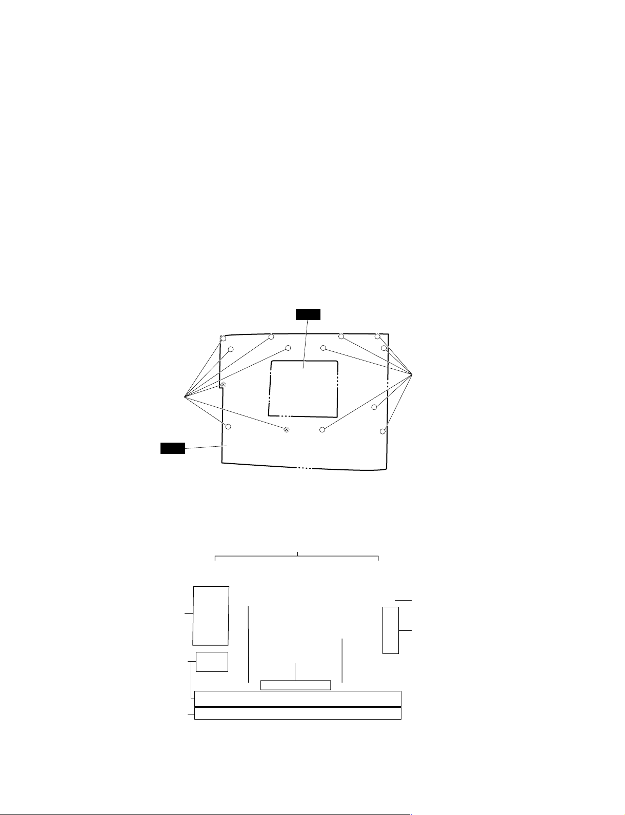
B. Top Section Disassembly Procedure
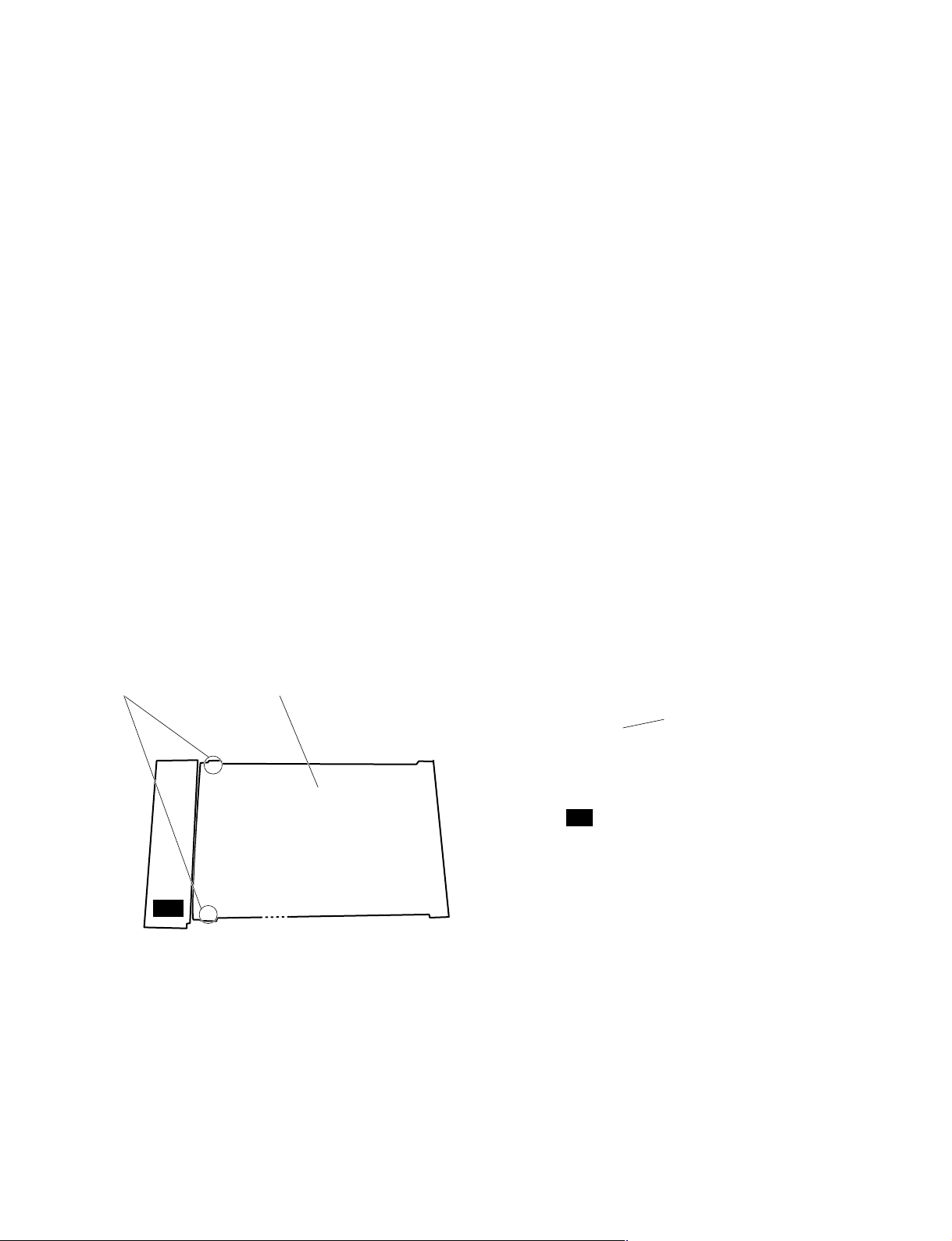
B-1. Sheet PN2 Assembly
(Time required: About 6 minutes)
B-1-1 Remove the f our (4) encoder knobs and the jog knob
from the control panel surface. (Fig.11)
B-1-2 Remove the top cover. (See procedure 1)
B-1-3 Remove the fifteen (15) screws marked [1190A].
The sheet PN2 assembly and PN2 protection sheet
can then be removed. (Fig.12)
* Remove the flat cables by releasing the claws
of the connectors CN002, CN003, and CN004
for the sheet PN2 assembly in the direction of
the arrow. (Photo 6)
* When replacing the sheet PN2 assembly, install
the PN2 protection sheet just as it was before
removal.
* The sheet PN2 assembly contains the following
buttons. (Photo 6)
• [20]: Button S LENS (Black) 14 pcs.
• [30]: Button S (Black) 11 pcs.
• [40]: Button L (M-Gray) 15 pcs.
• [50]: Button L LENS (Black) 5 pcs.
• [60]: Button L (Black) 2 pcs.
• [70]: Button, PLAY (White) 1 pc.
• [80]: Button, STOP (White) 1 pc.
• [90]: Button, FFW (White) 1 pc.
• [100]: Button, REW (White) 1 pc.
• [110]: Button, TOP (White) 1 pc.
• [120]: Button, REC (White) 1 pc.
B. トップ部の分解
B-1. シートPN2Ass y(所要時間:約6分)
B-1-1 コントロールパネル面より、エンコーダーノブ4個
とノブJOG1個を外します。(図11)
B-1-2 トップカバーを外します。(1項参照)
B-1-3 [1190A]のネジ15本を外して、シートPN2Ass yと
保護シートPN2を外します。(図12)
※ シートPN2Ass yのコネクタCN002、CN003、
CN004はツメを矢印の方向に解除してフラット
ケーブルを外します。(写真6)
※ シートPN2Ass yを交換する際には、保護シート
PN2を必ず元通りに取り付けてください。
※ シートPN2Ass yには下記のボタンがついていま
す。(写真6)
・[20]: ボタンS照光(黒) 14個
・[30]: ボタンS(黒) 11個
・[40]: ボタンL(灰) 15個
・[50]: ボタンL照光(黒) 5個
・[60]: ボタンL(黒) 2個
・[70]: ボタンTRPLAY(白) 1個
・[80]: ボタンTRSTOP(白) 1個
・[90]: ボタンTRFFW(白) 1個
・[100]: ボタンTRREW(白) 1個
・[110]: ボタンTRTOP(白) 1個
・[120]: ボタンTRREC(白) 1個
<Bottom view>
[1190A] x 15
[1192]
[1190E]
LCD holder
(ホルダーLCD)
<Top view>
26
Top cover
(トップカバー)
Encoder knob
(エンコーダーノブ)
Fader knob (Beige)
(フェーダーノブ(ベージュ))
Fig.11 (図11)
Jog knob
(ノブJOG)
Fader knob (Red)
(フェーダーノブ(赤))
ML
[1190D]
LCD
[1190E]
[1190B]
Sheet PN2 assembly
(シートPN2 Ass'y)
[1190]: Bind Head Tapping Screw-B (Bタイト+BIND)
3.0X6 MFZN2W3 (WE936300)
[1192]: Bind Head Tapping Screw-B (Bタイト+BIND)
3.0X8 MFZN2B3 (WE774400)
PN2 protection sheet
(保護シートPN2)
Fig.12 (図12)
[1192]
FD protection sheet
(保護シートFD)
FD
[50]:ButtonLLENS(Black)
(ボタンL照光(黒))
[20]:ButtonSLENS(Black)
(ボタンS照光(黒))
[30]:ButtonS(Black)
(ボタンS(黒))
[20]:ButtonSLENS(Black)
(ボタンS照光(黒))
[50]:ButtonLLENS(Black)
(ボタンL照光(黒))
[40]:ButtonL(M-Gray)
(ボタンL(灰))
[40]:ButtonL(M-Gray)
(ボタンL(灰))
[60]:ButtonL(Black)
(ボタンL(黒))
[70]:Button,PLAY(White)
(ボタンTRPLAY(白))
[120]:Button,REC(White)
(ボタンTRREC(白))
[90]:Button,FFW(White)(ボタンTRFFW(白))
[100]:Button,REW(White)(ボタンTRREW(白))
[110]:Button,TOP(White)(ボタンTRTOP(白))
[80]:Button,STOP(White)
(ボタンTRSTOP(白))
Claw(ツメ)
Claw
(ツメ)
• Sheet PN2 Assembly(シートPN2Ass y)
CN002CN002CN002CN003CN003CN003
CN004CN004
(ツメの部分を矢印の
方向に解除して、コネ
クタを外します。)
(ツメの部分を矢印の方向
に解除して、コネクタを外
します。)
Remove the connector by
releasing the claws in the
direction of the arrow.
Remove the connector
by releasing the claws
in the direction of the
arrow.
Photo 6 (写真6)
B-2. FD Circuit Board
(Time required: About 4 minutes)
B-2-1 Remove the twelve (12) fader knobs (beige) and
the fader knob (red) from the control panel surface.
(Fig.11)
B-2-2 Remove the top cover. (See procedure 1)
B-2-3 Remove the four (4) cable clamps. The FD
protection sheet can then be removed.
(Fig.12, Photo 7)
B-2-4 Remove the eight (8) screws marked [1190B]. The
FD circuit board can then be removed. (Fig.12)
* When replacing the FD circuit board, install the
FD protection sheet just as it was before
removal.
* During the installation, lock the cable clamps
securely to the FD circuit board.
AW2400
B-2. FDシート(所要時間:約4分)
B-2-1 コントロールパネル面より、フェーダーノブ(ベー
ジュ)12個とフェーダーノブ(赤)1個を外します。
(図11)
B-2-2 トップカバーを外します。(1項参照)
B-2-3 フラットクランプ4個を外して、保護シートFDを
外します。(図12、写真7)
B-2-4 [1190B]のネジ8本を外して、FDシートを外しま
す。(図12)
※ FDシートを交換する際には、保護シートFDを必ず
元通りに取り付けてください。
※ 組み付けの際は、フラットクランプをFDシートに
確実にロックしてください。
Cable clamp
(フラットクランプ)
FD protection sheet
(保護シートFD)
FD
Photo 7 (写真7)
(フラットクランプ)
Cable clamp
27
AW2400
B-3. PN1 Circuit Board
(Time required: About 6 minutes)
B-3-1 Remove the top cover. (See procedure 1)
B-3-2 Remo v e t he FD circuit board. (See procedure B-2-4)
B-3-3 Remove the fourteen (14) screws marked [1190C]. The
PN1 circuit board can then be removed. (Photo 8)
* The PN1 circuit board contains the following
buttons. (Photo 9)
• [20]: Button S (M-Gray) 3 pcs.
• [30]: Button S (Black) 4 pcs.
• [40]: Button L LENS (M-Gray) 23 pcs.
• [50]: Button L LENS (Black) 13 pcs.
• [60]: Button L (Black) 8 pcs.
• [70]: Button S LENS (Black) 4 pcs.
[1190C]
B-3. PN1シート(所要時間:約6分)
B-3-1 トップカバーを外します。(1項参照)
B-3-2 FDシートを外します。(B-2-4項参照)
B-3-3 [1190C]のネジ14本を外して、PN1シートを外しま
す。(写真8)
※ PN1シートには下記のボタンがついています。
(写真9)
・[20]: ボタンS(灰) 3個
・[30]: ボタンS(黒) 4個
・[40]: ボタンL照光(灰) 23個
・[50]: ボタンL照光(黒) 13個
・[60]: ボタンL(黒) 8個
・[70]: ボタンS照光(黒) 4個
LCD
[1190C]
PN1
[1190C]: Bind Head Tapping Screw-B (Bタイト+BIND)3.0X6 MFZN2W3 (WE936300)
• PN1 Circuit Board(PN1シート)
[40]:ButtonLLENS(M-Gray)(ボタンL照光(灰))
[60]:ButtonL(Black)
(ボタンL(黒))
[40]:ButtonLLENS(M-Gray)
(ボタンL照光(灰))
[50]:ButtonLLENS(Black)
(ボタンL照光(黒))
Photo 8 (写真8)
[20]:ButtonS(M-Gray)
(ボタンS(灰))
[20]:ButtonS(M-Gray)
(ボタンS(灰))
[30]:ButtonS(Black)
(ボタンS(黒))
Photo 9 (写真9)
[20]:ButtonS(M-Gray)
(ボタンS(灰))
[70]:ButtonSLENS(Black)
(ボタンS照光(黒))
28
AW2400
B-4. LCD Circuit Board
(Time required: About 3 minutes)
B-4-1 Remove the top cover. (See procedure 1)
B-4-2 Remove the four (4) screws marked [1190D]. The
LCD circuit board can then be removed. (Fig.12)
B-5. ML Circuit Board, LCD
(Time required: About 4 minutes each)
B-5-1 Remove the top cover. (See procedure 1)
B-5-2 Remove the four (4) screws marked [1190E], and
four (4) screws marked [1192]. The LCD holder can
then be removed along with the LCD circuit board.
(Fig.12)
B-5-3 ML Circuit Board
B-5-3-1
B-5-4 LCD
B-5-4-1
* The button S is not part of the ML circuit board.
Remove the ML circuit board. (Fig.12, Photo 10)
Remove the two (2) screws marked [1190F]. The
LCD can then be removed. (Photo 10)
When replacing the ML circuit board, remove
the button S from the ML circuit board and
install it to the new ML circuit board. (Photo 11)
B-4.
B-4-1 トップカバーを外します。(1項参照)
B-4-2 [1190D]のネジ4本を外して、LCDシートを外しま
B-5.
B-5-1 トップカバーを外します。(1項参照)
B-5-2 [1190E]のネジ4本と[1192]のネジ4本を外して、
B-5-3 MLシート
B-5-3-1 MLシートを外します。(図12、写真10)
B-5-4 液晶ディスプレイ
B-5-4-1 [1190F]のネジ2本を外して、液晶ディスプレイを
※ ボタンSはMLシートの構成部品ではありません。
LCDシート
す。(図12)
(所要時間:約3分)
MLシート、液晶ディスプレイ
(所要時間:各約4分)
LCDシートと共にホルダーLCDを外します。(図12)
外します。(写真10)
MLシートを交換する際には、MLシートからボタ
ンSを取り外して、新しいMLシートに取り付けて
ください。(写真11)
[1190F] LCD(液晶ディスプレイ)
ML
[1190F]: Bind Head Tapping Screw-B (Bタイト+BIND)
3.0X6 MFZN2W3 (WE936300)
Photo 10 (写真10)
Button S (M-Gray)
(ボタンS(灰))
ML
Photo 11 (写真11)
29
AW2400
LSI PIN DESCRIPTION(LSI端子機能表)
M66590FP-RB0S (X5423A00) USB DEVICE CONTROLLER ......................................................... 30
HD6417709SF133BV (X2081A00) CPU (SH3)................................................................................. 31
YSS910-V (XV988B00) DSP6 (Digital Signal Processor) .................................................................. 32
YSS919B-HZ (XZ693B00) DSP7 (Digital Signal Processor).............................................................. 33
YM3436D-FZ (XG948E00) DIR2 (Digital Format Interface Receiver)............................................... 34
S1D13700F01A100 (X5422A00) LCD CONTROLLER...................................................................... 34
AK5385AVF (X5364A00) ADC (Analog to Digital Converter) ............................................................ 35
AK4393VF-E2 (XW029A00) DAC (Digital to Analog Converter)........................................................ 35
M66590FP-RB0S (X5423A00) USB DEVICE CONTROLLER
PIN
NO.
1
2
3
4
5
6
7
8
9
10
11
12
13
14
15
16
17
18
19
20
21
22
23
24
25
26
27
28
29
30
31
32
33
34
35
36
37
38
39
40
41
42
43
44
45
46
47
48
49
50
DGND
VDD
DGND
AFEAVDD
AFEAGND
DFM
DHM
AFEAVDD
DHP
DFP
AFEAGND
AFEAVDD
AFEDGND
AFEDVDD
VBUS
TR_ON
RPU
BIASGND
REFRIN
BIASVDD
PLLGND
PLLVDD
DGND
VDD
TEST0
TEST1
TEST2
XOUT
XIN
DGND
VDD
VIF
A1
A2
A3
A4
A5
A6
A7
D0
D1
D2
D3
D4
D5
D6
D7
D8
D9
D10
I/O FUNCTIONNAME
I/O
I/O
I/O
I/O
O
O
I/O
I/O
I/O
I/O
I/O
I/O
I/O
I/O
I/O
I/O
I/O
–
–
–
–
–
–
–
–
–
–
I
I
–
I
–
–
–
–
–
I
I
I
I
–
–
–
I
I
I
I
I
I
I
Digital ground
Power supply
Digital ground
Analog power supply
Analog ground
USB full-speed data
USB Hi-speed data
Analog power supply
USB Hi-speed data
USB full-speed data
Analog ground
Analog power supply
Digital ground
Digital power supply
VBUS input
Pull-up power supply output
Pull-up control
BIAS ground
Reference input
PLL ground
PLL power supply
Digital ground
Power supply
Test
Oscillation output
Oscillation input
Digital ground
Power supply
Power supply
Address bus
Data bus
PIN
NO.
51
52
53
54
55
DGND
56
VDD
57
58
59
D16/PA0
60
D17/PA1
61
D18/PA2
62
D19/PA3
63
D20/PA4
64
D21/PA5
65
D22/PA6
66
D23/PA7
67
D24/PB0
68
D25/PB1
69
D26/PB2
70
D27/PB3
71
D28/PB4
72
D29/PB5
73
D30/PB6
74
D31/PB7
75
76
VDD
77
DGND
78
79
INT0
80
81
RD_N
82
WRO_N
83
WR1_N
WR2_N/EXTRG0_N
84
WR3_N/EXTRG1_N
85
CS_N
86
DREQ0
87
DACK0
88
DSTB0_N
89
DEND0
90
DBHE0
91
EXCTRL0
92
DREQ1
93
DACK1
94
DSTB1_N
95
DEND1
96
DBHE1
97
EXCTRL1
98
RST_N
99
100
D11
D12
D13
VIF
D14
D15
B32
VIF
SOF
VIF
I/O FUNCTIONNAME
I/O
I/O
I/O
I/O
I/O
I/O
I/O
I/O
I/O
I/O
I/O
I/O
I/O
I/O
I/O
I/O
I/O
I/O
I/O
I/O
I/O
O
O
O
I/O
I/O
O
I/O
I/O
DIO: IC005
Data bus
–
–
–
I
–
–
–
I
I
I
I
I
I
I
I
I
I
I
I
I
–
Power supply
Digital ground
Power supply
Data bus
Data bus / Port A
Data bus / Port B
Bus interface width select
Power supply
Digital ground
Power supply
Interrupt 0
SOF output
Read Strobe
Write Strobe
Write Strobe
Write Strobe / External trigger 0
Write Strobe / External trigger 1
Chip select
DMA request 0
DMA acknowledge 0
Split bus strobe 0
Transfer end 0
Byte Hi enable 0
External control 0
DMA request 1
DMA acknowledge 1
Split bus strobe 1
Transfer end 1
Byte Hi enable 1
External control 1
Reset
Power supply
30
 Loading...