


XICOR X9221YSM, X9221YSI, X9221YS, X9221YPM, X9221YPI Datasheet
...APPLICATION NOTES
A V A I L A B L E
AN20 • AN42 • AN44–48 • AN50 • AN52 • AN53 • AN73
AdvanceX9221TerminalInformVoltagetion±5V, 64 Taps
X9221
Dual E2POT™ Nonvolatile Digital Potentiometer
FEATURES
•Two E2POTs in One Package
•Two-Wire Serial Interface
•Register Oriented Format —Directly Write Wiper Position —Read Wiper Position
—Store as Many as Four Positions per Pot
•Instruction Format
—Quick Transfer of Register Contents to Resistor Array
•Low Power CMOS
•Direct Write Cell
—Endurance - 100,000 Writes per Register —Register Data Retention - 100 years
•8 Bytes of E2PROM memory
•3 Resistor Array Values
—2K Ω to 50KΩ Mask Programmable
•Resolution: 64 Taps each Pot
•20-Lead Plastic DIP and 20-Lead SOIC Packages
DESCRIPTION
The X9221 integrates two nonvolatile E2POT™ digitally controlled potentiometers on a monolithic CMOS microcircuit.
The X9221 contains two resistor arrays, each composed of 63 resistive elements. Between each element and at either end are tap points accessible to the wiper elements. The position of the wiper element on the array is controlled by the user through the two-wire serial bus interface.
Each resistor array has associated with it a wiper counter register and four 8-bit data registers that can be directly written and read by the user. The contents of the wiper counter register control the position of the wiper on the resistor array.
The data register may be read or written by the user. The contents of the data registers can be transferred to the wiper counter register to position the wiper. The current wiper position can be transferred to any one of its associated data registers.
FUNCTIONAL DIAGRAM
SCL 
SDA INTERFACE
  A0
A0  AND
AND
A1  CONTROL
A2 CIRCUITRY
A3 
R0 |
R1 |
WIPER |
VH0 |
|
|
|
|
|
|
COUNTER |
|
|
|
REGISTER |
|
R2 |
R3 |
(WCR) |
VL0 |
|
|
|
VW0 |
8
DATA
R0 |
R1 |
|
|
VH1 |
WIPER |
|
|
||
|
|
RESISTOR |
|
|
|
|
COUNTER |
|
|
|
|
REGISTER |
ARRAY |
|
R2 |
R3 |
(WCR) |
POT 1 |
VL1 |
|
|
VW1 |
||
|
|
|
|
3079 ILL F07.1
© Xicor, Inc. 1994, 1995, 1996 Patents Pending. |
1 |
Characteristics subject to change without notice |
3079-1.6 6/12/96 T1/C1/D0 NS |
|
|
|
|

X9221
PIN DESCRIPTIONS
Host Interface Pins
Serial Clock (SCL)
The SCL input is used to clock data into and out of the X9221.
Serial Data (SDA)
SDA is a bidirectional pin used to transfer data into and out of the device. It is an open drain output and may be wire-ORed with any number of open drain or open collector outputs. An open drain output requires the use of a pull-up resistor. For selecting typical values, refer to the guidelines for calculating typical values on the bus pull-up resistors graph.
Address
The Address inputs are used to set the least significant 4 bits of the 8-bit slave address. A match in the slave address serial data stream must be made with the Address input in order to initiate communication with the X9221
Potentiometer Pins
V |
(V |
– V ), V |
L |
(V |
L0 |
– V ) |
H |
H0 |
H1 |
|
L1 |
The VH and VL inputs are equivalent to the terminal connections on either end of a mechanical potentiometer.
V |
(V |
W0 |
– V ) |
W |
|
W1 |
The wiper outputs are equivalent to the wiper output of a mechanical potentiometer.
PIN CONFIGURATION
|
|
|
DIP/SOIC |
|
|
|
|
|
|
|
|
VW0 |
|
1 |
20 |
|
VCC |
|
|
||||
|
|
||||
VL0 |
|
2 |
19 |
|
RES |
VH0 |
|
3 |
18 |
|
RES |
|
|
||||
A0 |
|
4 |
17 |
|
RES |
|
|
||||
A2 |
|
5 |
16 |
|
A1 |
|
|
||||
|
|
|
X9221 |
|
|
VW1 |
|
6 |
15 |
|
A3 |
VL1 |
|
7 |
14 |
|
SCL |
|
|
||||
VH1 |
|
8 |
13 |
|
RES |
|
|
||||
SDA |
|
9 |
12 |
|
RES |
|
|
||||
VSS |
|
10 |
11 |
|
RES |
|
|
||||
|
|
||||
3079 ILL F01.1
PIN NAMES
Symbol |
Description |
|
|
SCL |
Serial Clock |
|
|
SDA |
Serial Data |
A0–A3 |
Address |
|
|
VH0–VH1, VL0–VL1 |
Potentiometers |
|
(terminal equivalent) |
VW0–VW1 |
Potentiometers |
|
(wiper equivalent) |
RES |
Reserved (Do not connect) |
|
|
3079 PGM T01
PRINCIPLES OF OPERATION
The X9221 is a highly integrated microcircuit incorporating two resistor arrays, their associated registers and counters and the serial interface logic providing direct communication between the host and the E2POT potentiometers.
Serial Interface
The X9221 supports a bidirectional bus oriented protocol. The protocol defines any device that sends data onto the bus as a transmitter and the receiving device as the receiver. The device controlling the transfer is a master and the device being controlled is the slave. The master will always initiate data transfers and provide the clock for both transmit and receive operations. Therefore, the X9221 will be considered a slave device in all applications.
Clock and Data Conventions
Data states on the SDA line can change only during SCL LOWperiods(tLOW).SDAstatechangesduringSCLHIGH are reserved for indicating start and stop conditions.
Start Condition
All commands to the X9221 are preceded by the start condition, which is a HIGH to LOW transition of SDA while SCL is HIGH (tHIGH). The X9221 continuously monitors the SDA and SCL lines for the start condition and will not respond to any command until this condition is met.
Stop Condition
All communications must be terminated by a stop condition, which is a LOW to HIGH transition of SDA while SCL is HIGH.
2
X9221
Acknowledge
Acknowledge is a software convention used to provide a positive handshake between the master and slave devices on the bus to indicate the successful receipt of data. The transmitting device, either the master or the slave, will release the SDA bus after transmitting eight bits. The master generates a ninth clock cycle and during this period the receiver pulls the SDA line LOW to acknowledge that it successfully received the eight bits of data. See Figure 7.
The X9221 will respond with an acknowledge after recognition of a start condition and its slave address and once again after successful receipt of the command byte. If the command is followed by a data byte the X9221 will respond with a final acknowledge.
Array Description
The X9221 is comprised of two resistor arrays. Each array contains 63 discrete resistive segments that are connected in series. The physical ends of each array are equivalent to the fixed terminals of a mechanical potentiometer (VH and VL inputs).
At both ends of each array and between each resistor segment is a FET switch connected to the wiper (VW) output. Within each individual array only one switch may be turned on at a time. These switches are controlled by the Wiper Counter Register (WCR). The six least significant bits of the WCR are decoded to select, and enable, one of sixty-four switches.
The WCR may be written directly, or it can be changed by transferring the contents of one of four associated data registers into the WCR. These data registers and the WCR can be read and written by the host system.
Device Addressing
Following a start condition the master must output the address of the slave it is accessing. The most significant four bits of the slave address are the device type identifier (refer to Figure 1 below). For the X9221 this is fixed as 0101[B].
Figure 1. Slave Address
DEVICE TYPE
IDENTIFIER
|
|
|
|
|
|
|
|
0 |
1 |
0 |
1 |
A3 |
A2 |
A1 |
A0 |
|
|
|
|
|
|
|
|
DEVICE ADDRESS
3079 ILL F08
The next four bits of the slave address are the device address. The physical device address is defined by the state of the A0-A3 inputs. The X9221 compares the serial data stream with the address input state; a successful compare of all four address bits is required for the X9221 to respond with an acknowledge.
Acknowledge Polling
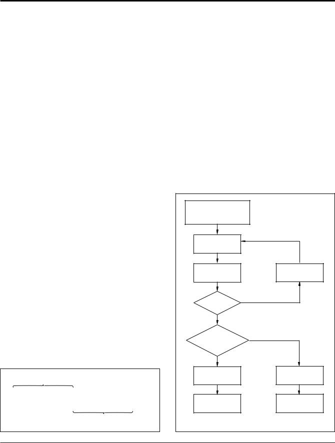
The disabling of the inputs, during the internal nonvolatile write operation, can be used to take advantage of the typical 5ms E2PROM write cycle time. Once the stop condition is issued to indicate the end of the nonvolatile write command the X9221 initiates the internal write cycle. ACK polling can be initiated immediately. This involves issuing the start condition followed by the device slave address. If the X9221 is still busy with the write operation no ACK will be returned. If the X9221 has completed the write operation an ACK will be returned and the master can then proceed with the next operation.
Flow 1. ACK Polling Sequence
NONVOLATILE WRITE |
|
||
COMMAND COMPLETED |
|
||
ENTER ACK POLLING |
|
||
ISSUE |
|
|
|
START |
|
|
|
ISSUE SLAVE |
|
ISSUE STOP |
|
ADDRESS |
|
||
|
|
||
ACK |
NO |
||
RETURNED? |
|||
|
|
||
YES |
|
|
|
FURTHER |
|
NO |
|
OPERATION? |
|
|
|
YES |
|
|
|
ISSUE |
|
ISSUE STOP |
|
INSTRUCTION |
|
||
|
|
||
PROCEED |
|
PROCEED |
|
|
|
3079 ILL F18 |
|
3
X9221
Instruction Structure
The next byte sent to the X9221 contains the instruction and register pointer information. The four most significant bits are the instruction. The next four bits point to one of two pots and when applicable they point to one of four associated registers. The format is shown below in Figure 2.
Figure 2. Instruction Byte Format
|
|
|
|
POTENTIOMETER |
|
||
|
|
|
|
|
SELECT |
|
|
I3 |
I2 |
I1 |
I0 |
0 |
P0 |
R1 |
R0 |
|
INSTRUCTIONS |
|
|
|
REGISTER |
||
|
|
|
|
|
|
SELECT |
|
3079 ILL F09.1
The four high order bits define the instruction. The sixth bit (P0) selects which one of the two potentiometers is to be affected by the instruction. The last two bits (R1 and R0) select one of the four registers that is to be acted upon when a register oriented instruction is issued.
Four of the nine instructions end with the transmission of the instruction byte. The basic sequence is illustrated in Figure 3. These two-byte instructions exchange data between the WCR and one of the data registers. A transfer from a data register to a WCR is essentially a write to a static RAM. The response of the wiper to this action will be delayed tSTPWV. A transfer from WCR’s
Figure 3. Two-Byte Command Sequence
current wiper position to a data register is a write to nonvolatile memory and takes a minimum of tWR to complete. The transfer can occur between either potentiometer and their associated registers or it may occur between both of the potentiometers and one of their associated registers.
Four instructions require a three-byte sequence to complete. These instructions transfer data between the host and the X9221; either between the host and one of the data registers or directly between the host and the WCR. These instructions are: Read WCR, read the current wiper position of the selected pot; Write WCR, change current wiper position of the selected pot; Read Data Register, read the contents of the selected nonvolatile register; Write Data Register, write a new value to the selected data register. The sequence of operations is shown in Figure 4.
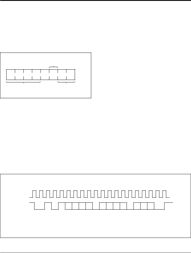
The Increment/Decrement command is different from the other commands. Once the command is issued and the X9221 has responded with an acknowledge, the master can clock the selected wiper up and/or down in one segment steps; thereby, providing a fine tuning
capability to the host. For each SCL clock pulse (tHIGH) while SDA is HIGH, the selected wiper will move one
resistor segment towards the VH terminal. Similarly, for each SCL clock pulse while SDA is LOW, the selected wiper will move one resistor segment towards the VL terminal. A detailed illustration of the sequence and timing for this operation are shown in Figures 5 and 6 respectively.
SCL
SDA
S 0 |
1 0 1 A3 A2 A1 A0 A |
I3 I2 I1 I0 |
0 P0 R1 R0 A |
S |
T |
C |
C |
T |
|
A |
K |
|
K |
O |
R |
|
|
|
P |
T |
|
|
|
|
3079 ILL F10
4

X9221
Figure 4. Three-Byte Command Sequence
SCL
SDA
S 0 1 |
0 1 A3 A2 A1 A0 A |
I3 I2 I1 I0 |
0 P0 R1 R0 A |
0 0 D5 D4 D3 D2 D1 D0 A |
S |
T |
C |
C |
C |
T |
|
A |
K |
|
K |
K |
O |
R |
|
|
|
|
P |
T |
|
|
|
|
|
3079 ILL F11
Figure 5. Increment/Decrement Command Sequence
SCL |
|
|
|
|
|
|
|
|
|
|
|
|
|
|
|
|
|
|
|
|
|
|
|
|
SDA |
|
|
|
|
|
|
|
|
|
|
|
|
|
|
|
X |
X |
|
|
|
|
|
|
|
S |
0 |
1 |
0 |
1 |
A3 |
A2 |
A1 |
A0 |
A |
I3 |
I2 |
I1 |
I0 |
0 |
P0 |
R1 |
R0 |
A |
I |
I |
I |
D |
D |
S |
T |
|
|
|
|
|
|
|
|
C |
|
|
|
|
|
|
|
|
C |
N |
N |
N |
E |
E |
T |
A |
|
|
|
|
|
|
|
|
K |
|
|
|
|
|
|
|
|
K |
C |
C |
C |
C |
C |
O |
R |
|
|
|
|
|
|
|
|
|
|
|
|
|
|
|
|
|
|
1 |
2 |
n |
1 |
n |
P |
T |
|
|
|
|
|
|
|
|
|
|
|
|
|
|
|
|
|
|
|
|
|
|
3079 ILL F12 |
|
|
|
|
|
|
|
|
|
|
|
|
|
|
|
|
|
|
|
|
|
|
|
|
||
Figure 6. Increment/Decrement Timing Limits
INC/DEC |
|
CMD |
tCLWV |
ISSUED |
|
SCL |
|
SDA |
|
VW |
VOLTAGE OUT |
|
|
|
3079 ILL F13 |
|
5 |
 Loading...