


XICOR X84641V20I-2,5, X84641V20I-1,8, X84641V20I, X84641V20-2,5, X84641V20-1,8 Datasheet
...APPLICATION NOTE
A V A I L A B L E
AN95 • AN103 • AN107
16K/64K/128K |
X84161/641/129 |
MPS EEPROM |
|
Port Saver EEPROM |
|
FEATURES
•Up to 10MHz data transfer rate
•25ns Read Access Time
•Direct Interface to Microprocessors and Microcontrollers
—Eliminates I/O port requirements
—No interface glue logic required
—Eliminates need for parallel to serial converters
•Low Power CMOS
—1.8V–3.6V, 2.5V–5.5V and 5V ±10% Versions
—Standby Current Less than 1 A
—Active Current Less than 1mA
•Byte or Page Write Capable
—32-Byte Page Write Mode
•Typical Nonvolatile Write Cycle Time: 2ms
•High Reliability
—100,000 Endurance Cycles
—Guaranteed Data Retention: 100 Years
DESCRIPTION
The Port Saver memories need no serial ports or special hardware and connect to the processor memory bus. Replacing bytewide data memory, the Port Saver uses bytewide memory control functions, takes a fraction of the board space and consumes much less power. Replacing serial memories, the Port Saver provides all the serial benefits, such as low cost, low power, low voltage, and small package size while releasing I/Os for more important uses.
The Port Saver memory outputs data within 25ns of an active read signal. This is less than the read access time of most hosts and provides “no-wait-state” operation. This prevents bottlenecks on the bus. With rates to 10 MHz, the Port Saver supplies data faster than required by most host read cycle specifications. This eliminates the need for software NOPs.
The Port Saver memories communicate over one line of the data bus using a sequence of standard bus read and write operations. This “bit serial” interface allows thePort Saver to work well in 8-bit, 16 bit, 32-bit, and 64-bit systems.
A Write Protect (WP) pin prevents inadvertent writes to the memory.
Xicor EEPROMs are designed and tested for applications requiring extended endurance. Inherent data retention is greater than 100 years.
BLOCK DIAGRAM |
|
|
|
|
|
|
|
System Connection |
|
Internal Block Diagram |
|||
|
|
|
MPS |
|||
|
P |
A15 |
WP |
|
|
H.V. GENERATION |
|
|
|
|
TIMING & CONTROL |
||
|
C |
|
|
|
|
|
|
DSP |
A0 |
CE |
|
|
|
|
ASIC |
D7 |
COMMAND |
|
EEPROM |
|
|
|
I/O |
|
|||
|
RISC |
|
DECODE |
X |
ARRAY |
|
|
D0 |
|
|
|||
|
|
OE |
AND |
DEC |
16K x 8 |
|
|
P0/CS |
|
CONTROL |
|
8K x 8 |
|
|
|
|
|
|||
|
OE |
|
LOGIC |
|
2K x 8 |
|
Ports |
P1/CLK |
WE |
|
|||
|
|
|
|
|||
Saved |
P2/DI |
WE |
|
|
|
|
|
P3/DO |
|
|
|
|
|
|
|
|
|
|
|
Y DECODE |
|
|
|
|
|
|
DATA REGISTER |
|
|
|
|
|
|
7008 FRM F02.1 |
Xicor, Inc. 1994, 1997Patents Pending |
|
1 |
|
Characteristics subject to change without notice |
||
7008-1.2 8/26/97 T2/C0/D0 SH |
|
|
|
|
||
|
|
|
|
|
||

X84161/641/129
PIN CONFIGURATIONS: Drawings are to the same scale, actual package sizes are shown in inches:
8-LEAD PDIP
8-LEAD SOIC
|
|
|
|
|
|
1 |
|
8 |
|
|
VCC |
|
|
|
||
|
CE |
|
|
|
|
|
|
|
|
|
||||||
|
I/O |
|
|
|
2 |
X84161 |
7 |
|
|
NC |
|
|
|
|||
|
|
|
|
|
.190 in. |
|||||||||||
|
|
|
|
|
|
|
X84641 |
6 |
|
|
|
|
|
|||
|
WP |
|
|
|
3 |
|
|
OE |
||||||||
VSS |
|
|
4 |
|
5 |
|
|
|
|
|
|
|
|
|||
|
|
|
|
|
WE |
|
|
|
|
|||||||
|
|
|
|
|
|
|
.230 in. |
|
|
|
|
|
|
|
|
|
|
|
|
|
|
|
|
|
|
|
|
|
|
|
|
|
|
|
|
|
|
|
|
14-LEAD SOIC |
|
|
|
|
|
|
||||
|
|
|
|
|
|
1 |
|
14 |
|
|
V CC |
|
|
|
||
|
CE |
|
|
|
|
|
|
|
|
|||||||
|
|
|
|
|
|
|
|
|
|
|||||||
|
I/O |
|
|
2 |
|
13 |
|
|
NC |
|
|
|
||||
|
|
|
|
|
|
|
|
|
||||||||
|
NC |
|
|
3 |
|
12 |
|
|
NC |
|
|
|
||||
|
|
|
|
|
|
|
|
|
||||||||
|
|
|
|
|
|
|
|
|
||||||||
|
NC |
|
|
4 |
X84129 |
11 |
|
|
NC |
|
|
|
||||
|
|
|
|
|
|
|
|
|||||||||
|
|
|
|
|
|
|
|
|||||||||
|
NC |
|
|
5 |
10 |
|
|
NC |
.390 in. |
|||||||
|
|
|
|
|
|
|||||||||||
|
|
|
|
|
|
|
9 |
|
|
|
|
|
|
|
|
|
|
WP |
|
|
|
6 |
|
|
|
OE |
|
|
|
||||
|
|
|
|
|
|
|
|
|
|
|
||||||
VSS |
|
|
|
|
8 |
|
|
|
|
|
|
|
||||
|
|
7 |
|
|
|
|
WE |
|
|
|
||||||
|
|
|
|
|
|
|
|
|
|
|
|
|||||
|
|
|
|
|
|
|
.230 in. |
|
|
|
|
|
|
|
|
|
|
|
|
|
|
|
|
|
|
|
|
|
|
|
|
|
|
|
|
|
|
|
|
|
|
|
|
|
|
|
|
|
|
|
|
|
|
|
|
|
|
8-LEAD TSSOP |
|
|
|
|
|
|
|
|
|
|
|
|
|
|||||||
|
NC |
|
|
1 |
|
|
|
|
|
|
|
8 |
|
|
|
OE |
|
|
|
|
|
|
|
|
|||
VCC |
|
|
|
|
2 |
|
X84161 |
7 |
|
|
|
WE |
|
|
|
|
.114 in. |
||||||||||
|
|
|
|
|
|
|
|
|
|
6 |
|
|
|
|
|
|
|
|
|
||||||||
|
CE |
|
|
|
|
3 |
|
|
|
|
|
WP |
|
|
|
||||||||||||
|
|
|
|
|
|
|
|
|
|
|
|
|
|
|
|
|
|
|
|||||||||
|
I/O |
|
|
|
4 |
|
|
|
|
|
|
|
5 |
|
|
|
VSS |
|
|
|
|
|
|
||||
|
|
|
|
|
|
|
|
|
|
|
|
|
|
|
|
|
|
|
|
|
|||||||
|
|
|
|
|
|
|
|
|
|
.252 in. |
|
|
|
|
|
|
|
|
|
|
|
|
|
||||
|
|
|
|
|
|
|
|
|
|
|
|
|
|
|
|
|
|
|
|
|
|
|
|
||||
|
|
|
|
|
|
|
|
|
|
|
|
|
|
|
|
|
|
|
|
|
|
|
|
||||
|
|
|
|
|
|
|
|
|
20-LEAD TSSOP |
|
|
|
|
|
|
|
|
|
|
|
|
|
|||||
|
NC |
|
|
|
1 |
|
|
|
|
|
|
|
20 |
|
|
|
NC |
|
|
|
|
|
|
||||
|
NC |
|
|
|
2 |
|
|
|
|
|
|
|
19 |
|
|
|
NC |
|
|
|
|
|
|
||||
|
CE |
|
|
|
3 |
|
|
|
|
|
|
|
18 |
|
|
|
VCC |
|
|
|
|
|
|
||||
|
|
|
|
|
|
|
|
|
|
|
|
|
|
|
|
||||||||||||
|
|
|
|
|
|
|
|
|
|
|
|
|
|
|
|
||||||||||||
|
I/O |
|
|
|
4 |
|
|
X84641 |
17 |
|
|
|
NC |
|
|
|
|
|
|
||||||||
|
|
|
|
|
|
|
|
|
|
|
|||||||||||||||||
|
NC |
|
|
|
5 |
|
|
16 |
|
|
|
NC |
|
|
.250 in. |
||||||||||||
|
|
|
|
|
|
||||||||||||||||||||||
|
NC |
|
|
|
6 |
|
|
|
|
|
|
|
15 |
|
|
|
NC |
|
|
|
|
|
|
||||
|
NC |
|
|
|
7 |
|
|
|
|
|
|
|
14 |
|
|
|
NC |
|
|
|
|
|
|
||||
|
|
|
|
|
|
|
|
|
|
|
|
|
|
|
|
||||||||||||
|
WP |
|
|
|
8 |
|
|
|
|
|
|
|
13 |
|
|
|
OE |
|
|
|
|
|
|
||||
|
|
|
|
|
|
|
|
|
|
|
|
|
|
|
|
||||||||||||
|
|
|
|
|
|
|
|
|
|
|
|
|
|
|
|
||||||||||||
|
VSS |
|
|
|
9 |
|
|
|
|
|
|
|
12 |
|
|
|
WE |
|
|
|
|
|
|
||||
|
|
|
|
|
|
|
|
|
|
|
|
|
|
|
|
||||||||||||
|
NC |
|
|
|
10 |
|
|
|
|
|
|
11 |
|
|
|
NC |
|
|
|
|
|
|
|||||
|
|
|
|
|
|
|
|
|
|
|
|
|
|
|
|
||||||||||||
|
|
|
|
|
|
|
|
|
|
|
|
|
|
|
|
||||||||||||
|
|
|
|
|
|
|
|
|
|
|
.252 in. |
|
|
|
|
|
|
|
|
|
|
|
|
|
|
|
|
|
|
|
|
|
|
|
|
|
|
|
|
|
|
|
|
|
|
|
|
|
|
|
|
|
|
||
|
|
|
|
|
|
|
|
|
|
|
|
|
|
|
|
|
|
|
|
|
|
|
|
|
|||
|
|
|
|
|
|
|
|
|
28-LEAD TSSOP |
|
|
|
|
|
|
|
|
|
|
|
|
|
|||||
|
NC |
|
|
|
|
|
|
|
|
|
|
|
|
|
|
NC |
|
|
|
|
|
|
|||||
|
|
|
1 |
|
|
|
|
|
|
|
28 |
|
|
|
|
|
|
|
|
|
|||||||
|
|
|
|
|
|
|
|
|
|
|
|
|
|
|
|||||||||||||
|
NC |
|
|
2 |
|
|
|
|
|
|
|
27 |
|
|
|
NC |
|
|
|
|
|
|
|||||
|
|
|
|
|
|
|
|
|
|
|
|
|
|
|
|||||||||||||
|
CE |
|
|
3 |
|
|
|
|
|
|
|
26 |
|
|
|
NC |
|
|
|
|
|
|
|||||
|
|
|
|
|
|
|
|
|
|
|
|
|
|
|
|||||||||||||
|
CE |
|
|
4 |
|
|
|
|
|
|
|
25 |
|
|
|
NC |
|
|
|
|
|
|
|||||
|
|
|
|
|
|
|
|
|
|
|
|
|
|
|
|||||||||||||
|
CE |
|
|
5 |
|
|
|
|
|
|
|
24 |
|
|
|
VCC |
|
|
|
|
|
|
|||||
|
|
|
|
|
|
|
|
|
|
|
|
|
|
|
|||||||||||||
|
I/O |
|
|
6 |
|
|
|
|
|
|
|
23 |
|
|
|
NC |
|
|
|
|
|
|
|||||
|
|
|
|
|
|
|
|
|
|
|
|
|
|
|
|||||||||||||
|
NC |
|
|
7 |
|
|
X84129 |
22 |
|
|
|
NC |
|
.394 in. |
|||||||||||||
|
|
|
|
||||||||||||||||||||||||
|
NC |
|
|
8 |
|
|
21 |
|
|
|
NC |
|
|
|
|
|
|
||||||||||
|
|
|
|
|
|
|
|
|
|||||||||||||||||||
|
NC |
|
|
9 |
|
|
|
|
|
|
|
20 |
|
|
|
NC |
|
|
|
|
|
|
|||||
|
WP |
|
|
10 |
|
|
|
|
|
|
19 |
|
|
|
OE |
|
|
|
|
|
|
||||||
|
VSS |
|
|
11 |
|
|
|
|
|
|
18 |
|
|
|
WE |
|
|
|
|
|
|
||||||
|
|
|
|
|
|
|
|
|
|
|
|
|
|
|
|||||||||||||
|
NC |
|
|
12 |
|
|
|
|
|
|
17 |
|
|
|
NC |
|
|
|
|
|
|
||||||
|
NC |
|
|
13 |
|
|
|
|
|
|
16 |
|
|
|
NC |
|
|
|
|
|
|
||||||
|
NC |
|
|
14 |
|
|
|
|
|
|
15 |
|
|
|
NC |
|
|
|
|
|
|
||||||
|
|
|
|
|
|
|
|
|
|
|
|
|
|
|
|||||||||||||
|
|
|
|
|
|
|
|
|
|
|
. 252 in. |
|
|
|
|
|
|
|
|
|
|
|
|
|
|
||
|
|
|
|
|
|
|
|
|
|
|
|
|
|
|
|
|
|
|
|
|
|
|
|
|
|||
|
|
|
|
|
|
|
|
|
|
|
|
|
|
|
|
|
|
|
|
|
|
|
|
|
|||
7008 FRM F01
PIN NAMES
|
I/O |
Data Input/Output |
||||
|
|
|
|
|
|
|
|
|
|
|
|
|
Chip Enable Input |
|
CE |
|||||
|
|
|
|
|
|
Output Enable Input |
|
OE |
|||||
|
|
|
|
|
|
Write Enable Input |
|
WE |
|||||
|
|
|
|
|
|
Write Protect Input |
|
WP |
|||||
|
VCC |
Supply Voltage |
||||
|
VSS |
Ground |
||||
|
NC |
No Connect |
||||
|
|
|
|
|
|
|
|
|
|
|
|
|
7008 FRM T01 |
PACKAGE
SELECTION GUIDE
8-Lead PDIP
84161 8-Lead SOIC
8-Lead TSSOP
8-Lead PDIP
84641 8-Lead SOIC
20-Lead TSSOP
8-Lead PDIP
84129 14-Lead SOIC
28-Lead TSSOP
7008 FRM T0A
PIN DESCRIPTIONS
Chip Enable (CE)
The Chip Enable input must be LOW to enable all read/ write operations. When CE is HIGH, the chip is deselected, the I/O pin is in the high impedance state, and unless a nonvolatile write operation is underway, the device is in the standby power mode.
Output Enable (OE)
The Output Enable input must be LOW to enable the output buffer and to read data from the device on the I/O line.
Write Enable (WE)
The Write Enable input must be LOW to write either data or command sequences to the device.
Data In/Data Out (I/O)
Data and command sequences are serially written to or serially read from the device through the I/O pin.
Write Protect (WP)
When the Write Protect input is LOW, nonvolatile writes to the device are disabled. When WP is HIGH, all functions, including nonvolatile writes, operate normally. If a nonvolatile write cycle is in progress, WP going LOW will have no effect on the cycle already underway, but will inhibit any additional nonvolatile write cycles.
2
X84161/641/129
DEVICE OPERATION
The X84161/641/129 are serial EEPROMs designed to interface directly with most microprocessor buses. Standard CE, OE, and WE signals control the read and write operations, and a single l/O line is used to send and receive data and commands serially.
Data Timing
Data input on the l/O line is latched on the rising edge of either WE or CE, whichever occurs first. Data output on the l/O line is active whenever both OE and CE are LOW. Care should be taken to ensure that WE and OE are never both LOW while CE is LOW.
Read Sequence
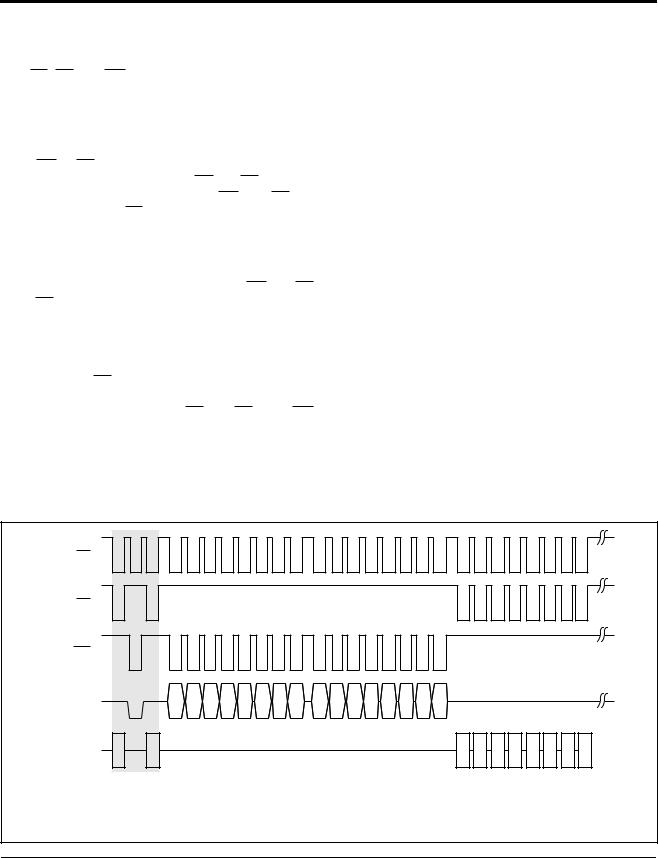
A read sequence consists of sending a 16-bit address followed by the reading of data serially. The address is written by issuing 16 separate write cycles (WE and CE LOW, OE HIGH) to the part without a read cycle between the write cycles. The address is sent serially, most significant bit first, over the I/O line. Note that this sequence is fully static, with no special timing restrictions, and the processor is free to perform other tasks on the bus whenever the device CE pin is HIGH. Once the 16 address bits are sent, a byte of data can be read on the I/O line by issuing 8 separate read cycles (OE and CE LOW, WE HIGH). At this point, writing a ‘1’ will terminate the read
sequence and enter the low power standby state, otherwise the device will await further reads in the sequential read mode.
Sequential Read
The byte address is automatically incremented to the next higher address after each byte of data is read. The data stored in the memory at the next address can be read sequentially by continuing to issue read cycles. When the highest address in the array is reached, the address counter rolls over to address $0000 and reading may be continued indefinitely.
Reset Sequence
The reset sequence resets the device and sets an internal write enable latch. A reset sequence can be sent at any time by performing a read/write “0”/read operation (see Figs. 1 and 2). This breaks the multiple read or write cycle sequences that are normally used to read from or write to the part. The reset sequence can be used at any time to interrupt or end a sequential read or page load. As soon as the write “0”cycle is complete, the part is reset (unless a nonvolatile write cycle is in progress). The second read cycle in this sequence, and any further read cycles, will read a HIGH on the l/O pin until a valid read sequence (which includes the address) is issued. The reset sequence must be issued at the beginning of both read and write sequences to be sure the device initiates these operations properly.
Figure 1. Read Sequence
CE |
|
|
|
|
|
|
|
|
|
|
OE |
|
|
|
|
|
|
|
|
|
|
WE |
|
|
|
|
|
|
|
|
|
|
I/O (IN) |
"0" |
A15 A14 A13 A12 A11 A10 |
A9 A8 |
A7 A6 A5 |
A4 |
A3 |
A2 |
A1 |
A0 |
|
|
|
|||||||||
I/O (OUT) |
|
|
|
|
|
|
|
|
D7 |
D6 |
|
RESET |
|
LOAD ADDRESS |
|
|
|
|
|
|
|
D5 D4 D3 D2 D1 D0 

READ DATA
WHEN ACCESSING: X84161 ARRAY: A15–A11=0 |
|
X84641 ARRAY: A15–A13=0 |
|
X84129 ARRAY: A15–A14=0 |
7008 FRM F04.1 |
3

X84161/641/129
Figure 2: Write Sequence
CE |
|
|
|
|
|
|
|
|
|
|
|
|
|
|
OE |
|
|
|
|
|
|
|
|
|
|
|
|
|
|
WE |
|
|
|
|
|
|
|
|
|
|
|
|
|
|
I/O (IN) |
"0" |
A15 A14 A13 A12 A11 A10 |
A9 A8 |
A7 A6 A5 |
A4 |
A3 |
A2 |
A1 |
A0 |
D7 D6 D5 D4 |
D3 |
D2 |
D1 |
D0 |
|
||||||||||||||
|
|
|
|
|
|
|
|
|
|
|
|
|
|
"1" |
I/O (OUT) |
|
|
|
|
|
|
|
|
|
|
|
|
|
"0" |
|
|
|
|
|
|
|
|
|
|
|
|
|
|
|
|
RESET |
LOAD ADDRESS |
|
|
|
|
|
LOAD DATA |
|
|
|
START |
||
|
|
|
|
|
|
|
|
|
|
|
|
|
|
NONVOLATILE |
WHEN ACCESSING: |
X84161 ARRAY: A15–A11=0 |
|
|
|
|
|
|
|
|
|
|
|
WRITE |
|
|
|
X84641 ARRAY: A15–A13=0 |
|
|
|
|
|
|
|
|
|
|
|
|
|
|
X84129 ARRAY: A15–A14=0 |
|
|
|
|
|
|
|
|
|
|
|
7008 FRM F05.1 |
|
|
|
|
|
|
|
|
|
|
|
|
|
|
|
Write Sequence
A nonvolatile write sequence consists of sending a reset sequence, a 16-bit address, up to 32 bytes of data, and then a special “starnonvolatile write cycle” command sequence.
The reset sequence is issued first (as described in the Reset Sequence section) to set an internal write enable latch. The address is written serially by issuing 16 separate write cycles (WE and CE LOW, OE HIGH) to the part without any read cycles between the writes. The address is sent serially, most significant bit first, on the l/O pin. Up to 32 bytes of data are written by issuing a multiple of 8 write cycles. Again, no read cycles are allowed between writes.
The nonvolatile write cycle is initiated by issuing a special read/write “1”/read sequence.The first read cycle ends the page load, then the write “1”followed by a read starts the nonvolatile write cycle. The device recognizes 32byte pages (e.g., beginning at addresses XXXXXX00000 for X84161).
When sending data to the part, attempts to exceed the upper address of the page will result in the address counter “wrapping-around” to the first address on the
page, where data loading can continue. For this reason, sending more than 256 consecutive data bits will result in overwriting previous data.
A nonvolatile write cycle will not start if a partial or incomplete write sequence is issued. The internal write enable latch is reset when the nonvolatile write cycle is completed and after an invalid write to prevent inadvertent writes. Note that this sequence is fully static, with no special timing restrictions. The processor is free to perform other tasks on the bus whenever the chip enable pin (CE) is HIGH.
Nonvolatile Write Status
The status of a nonvolatile write cycle can be determined at any time by simply reading the state of the l/O pin on the device. This pin is read when OE and CE are LOW and WE is HIGH. During a nonvolatile write cycle the l/O pin is LOW. When the nonvolatile write cycle is complete, the l/O pin goes HIGH. A reset sequence can also be issued during a nonvolatile write cycle with the same result: I/O is LOW as long as a nonvolatile write cycle is in progress, and l/O is HIGH when the nonvolatile write cycle is done.
4

X84161/641/129
Low Power Operation
The device enters an idle state, which draws minimal current when:
—an illegal sequence is entered. The following are the more common illegal sequences:
•Read/Write/Write—an y time
•Read/Write ‘1’—When wr iting the address or writing data.
•Write ‘1’—when reading data
•Read/Read/Write ‘1’—after data is wr itten to device, but before entering the NV write sequence.
—the de vice powers-up;
—a non volatile write operation completes.
While a sequential read is in progress, the device remains in an active state. This state draws more current than the idle state, but not as much as during a read itself. To go back to the lowest power condition, an invalid condition is created by writing a ‘1’ after the last bit of a read operation.
Write Protection
The following circuitry has been included to prevent inadvertent nonvolatile writes:
—The inter nal Write Enable latch is reset upon power-up.
—A reset sequence m ust be issued to set the internal write enable latch before starting a write sequence.
—A special “starnonvolatile write” command sequence is required to start a nonvolatile write cycle.
—The inter nal Write Enable latch is reset automatically at the end of a nonvolatile write cycle.
—The inter nal Write Enable latch is reset and remains reset as long as the WP pin is LOW, which blocks all nonvolatile write cycles.
—The inter nal Write Enable latch resets on an invalid write operation.
SYMBOL TABLE
|
WAVEFORM INPUTS |
OUTPUTS |
||||||||
|
|
|
|
|
|
|
|
|
Must be |
Will be |
|
|
|
|
|
|
|
|
|
||
|
|
|
|
|
|
|
|
|
steady |
steady |
|
|
|
|
|
|
|
|
|
May change |
Will change |
|
|
|
|
|
|
|
|
|
||
|
|
|
|
|
|
|
|
|
from LOW to |
from LOW to |
|
|
|
|
|
|
|
|
|
HIGH |
HIGH |
|
|
|
|
|
|
|
|
|
||
|
|
|
|
|
|
|
|
|
May change |
Will change |
|
|
|
|
|
|
|
|
|
||
|
|
|
|
|
|
|
|
|
from HIGH to |
from HIGH to |
|
|
|
|
|
|
|
|
|
LOW |
LOW |
|
|
|
|
|
|
|
|
|
||
|
|
|
|
|
|
|
|
|
Don’t Care: |
Changing: |
|
|
|
|
|
|
|
|
|
||
|
|
|
|
|
|
|
|
|
Changes |
State Not |
|
|
|
|
|
|
|
|
|
Allowed |
Known |
|
|
|
|
|
|
|
|
|
||
|
|
|
|
|
|
|
|
|
N/A |
Center Line |
|
|
|
|
|
||||||
|
|
|
|
|
|
|
|
|
|
is High |
|
|
|
|
|
|
|
|
|
|
|
|
|
|
|
|
|
|
|
|
|
Impedance |
|
|
|
|
|
|
|
|
|
|
|
|
|
|
|
|
|
|
|
|
|
|
5

X84161/641/129
ABSOLUTE MAXIMUM RATINGS* |
*COMMENT |
Temperature under Bias ...................... |
–65°C to +135°C |
Storage Temperature ........................... |
–65°C to +150°C |
Terminal Voltage with |
|
Respect to VSS ....................................... |
–1V to +7V |
DC Output Current................................................... |
5mA |
Lead Temperature (Soldering, 10 seconds) |
..........300°C |
||
RECOMMENDED OPERATING CONDITIONS |
|||
|
|
|
|
Temperature |
Min. |
|
Max. |
|
|
|
|
Commercial |
0°C |
|
+70 °C |
|
|
|
|
Industrial |
–40°C |
|
+85 °C |
|
|
|
|
Military† |
–55°C |
|
+125°C |
|
|
|
|
Stresses above those listed under “Absolute Maximum Ratings” may cause permanent damage to the device. This is a stress rating only and the functional operation of the device at these or any other conditions above those indicated in the operational sections of this specification is not implied. Exposure to absolute maximum rating conditions for extended periods may affect device reliability.
Supply Voltage |
Limits |
|
|
X84161/641/129 |
5V ±10% |
|
|
X84161/641/129 – 2.5 |
2.5V to 5.5V |
|
|
X84161/641/129 – 1.8 |
1.8V to 3.6V |
|
|
Notes: † Contact factory for Military availability |
7008 FRM T02 |
|
|
|
|
|
|
|
|
|
7008 FRM T03 |
||
D.C. OPERATING CHARACTERISTICS (VCC = 5V ±10%) |
|
|
|
|
|
|
|
|
|
||||
(Over the recommended operating conditions, unless otherwise specified.) |
|
|
|
|
|
|
|
||||||
|
|
|
|
|
|
|
|
|
|
|
|
|
|
|
|
|
Limits |
|
|
|
|
|
|
|
|
|
|
|
|
|
|
|
|
|
|
|
|||||
Symbol |
Parameter |
Min. |
Max. |
Units |
|
|
|
Test Conditions |
|||||
|
|
|
|
|
|
|
|
|
|
|
|
||
ICC1 |
VCC Supply Current (Read) |
|
1 |
mA |
|
|
|
= VIL, |
|
|
= VIH, |
||
|
OE |
WE |
|||||||||||
|
|
|
|
|
|
|
I/O = Open, |
CE |
clocking @ 10MHz |
||||
|
|
|
|
|
|
|
|
||||||
ICC2 |
VCC Supply Current (Write) |
|
2 |
mA |
|
ICC During Nonvolatile Write Cycle |
|||||||
|
|
All Inputs at CMOS Levels |
|||||||||||
|
|
|
|
|
|
|
|||||||
|
|
|
|
|
|
|
|
||||||
ISB1 |
VCC Standby Current |
|
1 |
A |
|
|
= VCC, Other Inputs = VCC or VSS |
||||||
|
CE |
||||||||||||
ILI |
Input Leakage Current |
|
10 |
A |
|
VIN = VSS to VCC |
|||||||
ILO |
Output Leakage Current |
|
10 |
A |
|
VOUT = VSS to VCC |
|||||||
V |
(1) |
Input LOW Voltage |
–0.5 |
V x 0.3 |
V |
|
|
|
|
|
|
|
|
|
lL |
|
|
CC |
|
|
|
|
|
|
|
|
|
VIH (1) |
Input HIGH Voltage |
VCC x 0.7 |
VCC + 0.5 |
V |
|
|
|
|
|
|
|
|
|
VOL |
Output LOW Voltage |
|
0.4 |
V |
|
IOL = 2.1mA |
|||||||
VOH |
Output HIGH Voltage |
VCC – 0.8 |
|
V |
|
IOH = –1mA |
|||||||
7008 FRM T04.2
Notes: (1) VIL Min. and VIH Max. are for reference only and are not tested.
6
 Loading...