


XICOR X24001SM-3, X24001SM-2,7, X24001SM, X24001SI-3, X24001SI-2,7 Datasheet
...X24001
128 Bit |
X24001 |
16 x 8 Bit |
Identi™ PROM
FEATURES
•2.7V to 5.5V Power Supply
•128 Bit Serial E2PROM
•Low Power CMOS
—Active Current Less Than 1mA —Standby Current Less Than 50 μA
•Internally Organized 16 x 8
•2 Wire Serial Interface
•High Voltage Programmable Only —V PGM, 12V to 15V
•Push/Pull Output
•High Reliability
—Data Retention: 100 Years
•Available Packages —8-Lead MSOP —8-Lead PDIP —8-Lead SOIC
DESCRIPTION
The X24001 is a CMOS 128 bit serial E2PROM, internally organized as 16 x 8. The X24001 features a serial interface and software protocol allowing operation on a simple two wire bus.
The X24001 is ideally suited for identification applications such as serial numbers or device revision numbers which need to be stored and retrieved electronically.
VPGM is used to enable writes to the device. This provides full protection of the data in the user’s environment where VPGM is not available.
Xicor E2PROMs are designed and tested for applications requiring extended endurance. Inherent data retention is greater than 100 years.
The X24001 is fabricated with Xicor’s Advanced CMOS Floating Gate technology.
FUNCTIONAL DIAGRAM |
PIN CONFIGURATION |
SCL |
|
|
CONTROL |
|
|
COMMAND/ADDRESS |
|
|
MSOP/DIP/SOIC |
|
|
||
|
|
LOGIC |
|
|
REGISTER |
|
|
|
|
||||
|
|
|
|
|
|
|
|
|
|
|
|||
|
|
|
|
|
|
|
|
NC |
|
1 |
8 |
|
VCC |
|
|
|
|
|
|
|
|
|
|
||||
|
|
|
|
|
|
|
|
|
|
||||
|
|
|
|
|
|
|
|
NC |
|
2 |
7 |
|
NC |
|
|
|
|
|
|
|
|
|
|
|
X24001 |
|
|
|
|
|
INPUT/ |
|
|
SHIFT REGISTER |
NC |
|
3 |
6 |
|
SCL |
|
SDA |
|
|
OUTPUT |
|
|
VSS |
|
4 |
5 |
|
SDA |
||
|
|
|
|
|
|
||||||||
|
|
|
BUFFER |
|
|
|
|
|
|||||
|
|
|
|
|
|
|
|
|
|
|
|
||
|
|
|
|
|
|
|
|
|
|
|
|
|
|
|
|
|
|
|
|
|
|
|
|
|
3830 FHD F02.1 |
||
|
|
|
|
|
|
|
|
|
|
|
|
|
|
|
|
|
|
|
|
|
MEMORY ARRAY |
|
|
|
|
|
|
|
|
|
|
|
|
|
|
|
|
|
|
|
|
|
|
|
|
|
|
|
3830 FHD F01 |
|
|
|
|
|
|
IDENTI™ PROM is a trademark of Xicor, Inc.
© Xicor, Inc. 1991, 1995, 1996 Patents Pending |
1 |
Characteristics subject to change without notice |
3830-1.5 6/10/96 T2/C1/D0 NS |
|
|
|
|

X24001
PIN DESCRIPTIONS
Serial Clock (SCL)
The SCL input is used to clock all data into and out of the device.
Serial Data (SDA)
SDA is a bidirectional pin used to transfer data into and out of the device. It is a push/pull output and does not require the use of a pull-up resistor. During the programming operation, SDA is an input.
PIN NAMES
Symbol |
Description |
|
|
NC |
No Connect |
|
|
VSS |
Ground |
VCC |
Supply Voltage |
SDA |
Serial Data |
|
|
SCL |
Serial Clock |
|
|
3830 PGM T01
DEVICE OPERATION
The X24001 supports a bidirectional bus oriented protocol. The protocol defines any device that sends data onto the bus as a transmitter and the receiving device as the receiver. The device controlling the transfer is a master and the device being controlled is the slave. The master will always initiate data transfers and provide the clock for both transmit and receive operations. Therefore, the X24001 will be considered a slave in all applications.
Clock and Data Conventions
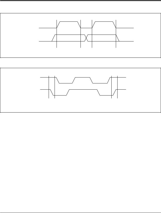
Data states on the SDA line can change only during SCL LOW. SDA state changes during SCL HIGH are reserved for indicating start and stop conditions. Refer to Figures 1 and 2.
Start Condition
All commands are preceded by the start condition, which is a HIGH to LOW transition of SDA when SCL is HIGH. The X24001 continuously monitors the SDA and SCL lines for the start condition and will not respond to any command until this condition has been met.
A start may be issued to terminate the input of a control word or the input of data to be written. This will reset the device and leave it ready to begin a new read or write command. Because of the push/pull output, a start cannot be generated while the part is outputting data. Starts are also inhibited while a write is in progress.
Stop Condition
The stop condition is a LOW to HIGH transition of SDA when SCL is HIGH. The stop condition is used to reset the device during a command or data input sequence and will leave the device in the standby mode. As with starts, stops are inhibited when outputting data and while a write is in progress.
2
X24001
Figure 1. Data Validity
SCL
SDA
DATA STABLE DATA
CHANGE
3830 FHD F03
Figure 2. Definition of Start and Stop Conditions
SCL
SDA
START CONDITION |
STOP CONDITION |
3830 FHD F04
3

X24001
Programming Operation
Programming of the X24001 is performed one byte at a time. After each byte is written, a delay equal to the write cycle time of 5ms must be observed before initiating the next write cycle.
The sequence of operations is: first raise the SCL pin to VPGM and generate a HIGH to LOW transition of SDA (programming mode start). This is followed by eight bits of data containing the program command bits, four address bits and two don’t care bits, immediately followed by the 8-bit data byte.
The timing of the operation conforms to the standard A.C. timing requirements and follows the sequence shown below. After generating the Programming Mode start condition the SCL HIGH level can be either VIH or VPGM.
Figure 3. Programming Sequence
Factory Programming Service
The X24001 can be programmed with customer specific data prior to shipment. The data programmed can be in two forms: static data pattern where there is no change in the data in a group of devices or sequential data, such as a base number incremented by one for each device tested and shipped.
Customers requiring one of these services should contact their local sales office for ordering procedures and service charges.
VPGM |
|
SCL |
|
VIH |
S |
|
T |
|
A |
|
R |
|
T |
SDA |
0 1 A3 A2 A1 A0 XX XX D7 D6 D5 D4 D3 D2 D1 D0 |
3830 FHD F05.1
4
 Loading...