


W29C020S-90B
Winbond Electronics W29C020S-90B, W29C020S-90A, W29C020S-90, W29C020S-70B, W29C020S-70A Datasheet
...
W29C020
256K × 8 CMOS FLASH MEMORY
GENERAL DESCRIPTION
The W29C020 is a 2-megabit, 5-volt only CMOS flash memory organized as 256K × 8 bits. The
device can be written (erased and programmed) in-system with a standard 5V power supply. A 12-volt
VPP is not required. The unique cell architecture of the W29C020 results in fast write (erase/program)
operations with extremely low current consumption compared to other comparable 5-volt flash
memory products. The device can also be written (erased and programmed) by using standard
EPROM programmers.
FEATURES
• Single 5-volt write (erase and program)
operations
• Fast page-write operations
− 128 bytes per page
− Page write (erase/program) cycle: 10 mS
(max.)
− Effective byte-write (erase/program) cycle
time: 39 µS
− Optional software-protected data write
• Fast chip-erase operation: 50 mS
• Two 8 KB boot blocks with lockout
• Typical page write (erase/program) cycles:
100/1K/10K
• Read access time: 70/90/120 nS
• Ten-year data retention
• Software and hardware data protection
• Low power consumption
− Active current: 25 mA (typ.)
− Standby current: 20 µA (typ.)
• Automatic write (erase/program) timing with
internal VPP generation
• End of write (erase/program) detection
− Toggle bit
− Data polling
• Latched address and data
• All inputs and outputs directly TTL compatible
• JEDEC standard byte-wide pinouts
• Available packages: 32-pin 600 mil DIP, 450 mil
SOP, TSOP, and 32-pin PLCC
Publication Release Date: February 1998
- 1 - Revision A3
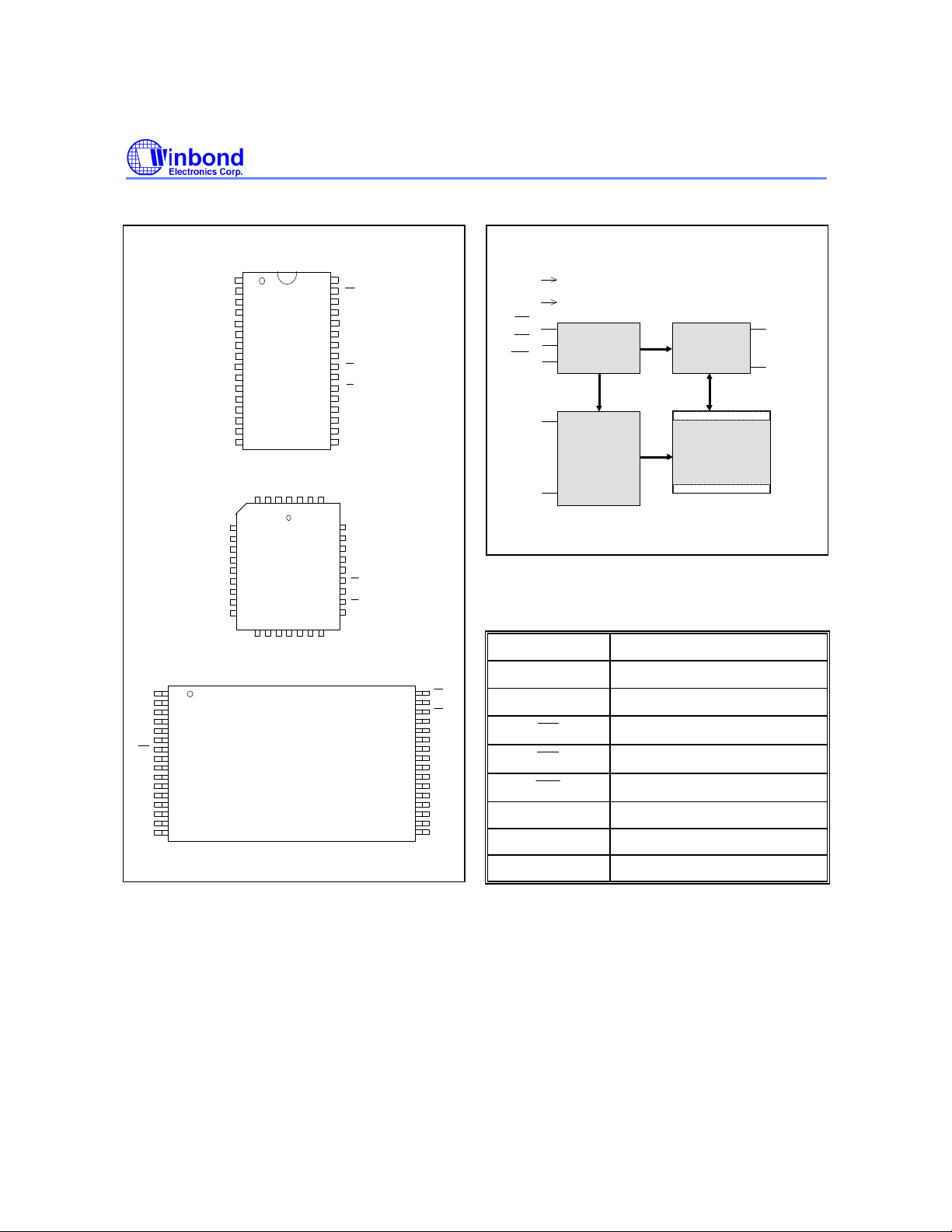
PIN CONFIGURATIONS BLOCK DIAGRAM
1
789
111213
14
16
V
DD
E
3
4
678
DQ1
DQ2
V
A13
DD
CE
OE
WE
W29C020
32-pin
DIP
A
16N
C
32-pin
PLCC
G
D
N
Q
D
3
32-pin
TSOP
32
31
WE
30
A17
29
A14
28
A13
27
A8
26
A9
25
A11
24
OE
23
A10
22
CE
21
DQ7
20
DQ6
19
DQ5
18
DQ4
17
DQ3
V
/
A
D
W
1
D
7
30313212
29
A14
28
A13
27
A8
26
A9
25
A11
24
OE
23
A10
22
CE
21
DQ7
20191817161514
D
D
D
Q
Q
Q
4
5
6
NC
2
A16
3
A15
4
A12
5
A7
6
A6
A5
A4
A3
10
A2
A1
A0
DQ0
DQ1
15
DQ2
GND
A
A
1
1
2
5
34
5
A7
6
A6
7
A5
8
A4
9
A3
10
A2
11
A1
12
A0
13
DQ0
D
D
Q
Q
1
2
A11
2
A9
A8
5
A14
A17
WE
9
NC
10
A16
11
A15
12
A12
13
A7
14
A6
15
A5
16 A3
A4
V
DD
V
SS
CE
OE
WE
A0
CONTROL
OUTPUT
BUFFER
8K Byte Boot Block (Optional)
DQ0
.
.
DQ7
.
CORE
ARRAY
8K Byte Boot Block (Optional)
A17
.
DECODER
.
PIN DESCRIPTION
SYMBOL PIN NAME
A0−A17
32
OE
A10
31
30
CE
DQ7
29
DQ6
28
DQ5
27
DQ4
26
DQ3
25
GND
24
23
22
DQ0
21
20
A0
A1
19
A2
18
17
DQ0−DQ7
VDD Power Supply
GND Ground
Address Inputs
Data Inputs/Outputs
Chip Enable
Output Enable
Write Enable
NC No Connection
- 2 -

W29C020
WE
FUNCTIONAL DESCRIPTION
Read Mode
The read operation of the W29C020 is controlled by CE and OE, both of which have to be low for
the host to obtain data from the outputs. CE is used for device selection. When CE is high, the chip
is de-selected and only standby power will be consumed. OE is the output control and is used to gate
data from the output pins. The data bus is in high impedance state when either CE or OE is high.
Refer to the read cycle timing waveforms for further details.
Page Write Mode
The W29C020 is written (erased/programmed) on a page basis. Every page contains 128 bytes of
data. If a byte of data within a page is to be changed, data for the entire page must be loaded into the
device. Any byte that is not loaded will be erased to "FF hex" during the write operation of the page.
The write operation is initiated by forcing CE and WE low and OE high. The write procedure
consists of two steps. Step 1 is the byte-load cycle, in which the host writes to the page buffer of the
device.
Step 2 is an internal write (erase/program) cycle, during which the data in the page buffers are
simultaneously written into the memory array for non-volatile storage.
During the byte-load cycle, the addresses are latched by the falling edge of either CE or WE,
whichever occurs last. The data are latched by the rising edge of either CE or
occurs first. If the host loads a second byte into the page buffer within a byte-load cycle time (TBLC) of
200 µS after the initial byte-load cycle, the W29C020 will stay in the page load cycle. Additional bytes
can then be loaded consecutively. The page load cycle will be terminated and the internal write
(erase/program) cycle will start if no additional byte is loaded into the page buffer A7 to A17 specify
the page address. All bytes that are loaded into the page buffer must have the same page address.
A0 to A6 specify the byte address within the page. The bytes may be loaded in any order; sequential
loading is not required.
In the internal write cycle, all data in the page buffers, i.e., 128 bytes of data, are written
simultaneously into the memory array. Before the completion of the internal write cycle, the host is
free to perform other tasks such as fetching data from other locations in the system to prepare to
write the next page.
, whichever
Software-protected Data Write
The device provides a JEDEC-approved optional software-protected data write. Once this scheme is
enabled, any write operation requires a three-byte command sequence (with specific data to a
specific address) to be performed before the data load operation. The three-byte load command
sequence begins the page load cycle, without which the write operation will not be activated. This
write scheme provides optimal protection against inadvertent write cycles, such as cycles triggered by
noise during system power-up and power-down.
The W29C020 is shipped with the software data protection enabled. To enable the software data
protection scheme, perform the three-byte command cycle at the beginning of a page load cycle. The
device will then enter the software data protection mode, and any subsequent write operation must be
preceded by the three-byte command sequence cycle. Once enabled, the software data protection
Publication Release Date: February 1998
- 3 - Revision A3

W29C020
DATA
will remain enabled unless the disable commands are issued. A power transition will not reset the
software data protection feature. To reset the device to unprotected mode, a six-byte command
sequence is required. For information about specific codes, see the Command Codes for Software
Data Protection in the Table of Operating Modes. For information about timing waveforms, see the
timing diagrams below.
Hardware Data Protection
The integrity of the data stored in the W29C020 is also hardware protected in the following ways:
(1) Noise/Glitch Protection: A WE pulse of less than 15 nS in duration will not initiate a write cycle.
(2) VDD Power Up/Down Detection: The write operation is inhibited when VDD is less than 2.5V.
(3) Write Inhibit Mode: Forcing OE low, CE high, or WE high will inhibit the write operation. This
prevents inadvertent writes during power-up or power-down periods.
(4) VDD power-on delay: When VDD reaches its sense level, the device will automatically timeout for
5 mS before any write (erase/program) operation.
Chip Erase Modes
The entire device can be erased by using a six-byte software command code. See the Software Chip
Erase Timing Diagram.
Boot Block Operation
There are two boot blocks (8K bytes each) in this device, which can be used to store boot code. One
of them is located in the first 8K bytes and the other is located in the last 8K bytes of the memory.
The first 8K or last 8K of the memory can be set as a boot block by using a seven-byte command
sequence.
See Command Codes for Boot Block Lockout Enable for the specific code. Once this feature is set
the data for the designated block cannot be erased or programmed (programming lockout); other
memory locations can be changed by the regular programming method. Once the boot block
programming lockout feature is activated, the chip erase function will be disabled. In order to detect
whether the boot block feature is set on the two 8K blocks, users can perform a six-byte command
sequence: enter the product identification mode (see Command Codes for Identification/Boot Block
Lockout Detection for specific code), and then read from address "00002 hex" (for the first 8K bytes)
or "3FFF2 hex" (for the last 8K bytes). If the output data is "FF hex," the boot block programming
lockout feature is activated; if the output data is "FE hex," the lockout feature is deactivated and the
block can be programmed.
To return to normal operation, perform a three-byte command sequence to exit the identification
mode. For the specific code, see Command Codes for Identification/Boot Block Lockout Detection.
Data Polling (DQ7)- Write Status Detection
The W29C020 includes a data polling feature to indicate the end of a write cycle. When the
W29C020 is in the internal write cycle, any attempt to read DQ7 from the last byte loaded during the
page/byte-load cycle will receive the complement of the true data. Once the write cycle is completed.
DQ7 will show the true data. See the
Polling Timing Diagram.
- 4 -
W29C020
WE
CEOEWE
Toggle Bit (DQ6)- Write Status Detection
In addition to data polling, the W29C020 provides another method for determining the end of a write
cycle. During the internal write cycle, any consecutive attempts to read DQ6 will produce alternating
0's and 1's. When the write cycle is completed, this toggling between 0's and 1's will stop. The device
is then ready for the next operation. See Toggle Bit Timing Diagram.
Product Identification
The product ID operation outputs the manufacturer code and device code. The programming
equipment automatically matches the device with its proper erase and programming algorithms.
The manufacturer and device codes can be accessed through software or by hardware operation. In
the software access mode, a six-byte command sequence can be used to access the product ID. A
read from address "00000 hex" outputs the manufacturer code "DA hex." A read from address "00001
hex" outputs the device code "45 hex." The product ID operation can be terminated by a three-byte
command sequence.
In the hardware access mode, access to the product ID is activated by forcing CE and OE low,
high, and raising A9 to 12 volts.
TABLE OF OPERATING MODES
Operating Mode Selection
Operating Range: 0 to 70° C (Ambient Temperature), VDD = 5V ±10%, VSS = 0V, VHH = 12V
MODE PINS
ADDRESS DQ.
Read VIL VIL VIH AIN Dout
Write VIL VIH VIL AIN Din
Standby VIH X X X High Z
Write Inhibit X VIL X X High Z/DOUT
X X VIH X High Z/DOUT
Output Disable X VIH X X High Z
5-Volt Software Chip Erase VIL VIH VIL AIN DIN
Product ID VIL VIL VIH
VIL VIL VIH
A0 = VIL; A1−A17 = VIL;
A9 = VHH
A0 = VIH; A1−A17 = VIL;
A9 = VHH
Manufacturer Code DA
(Hex)
Device Code
45 (Hex)
Publication Release Date: February 1998
- 5 - Revision A3
W29C020
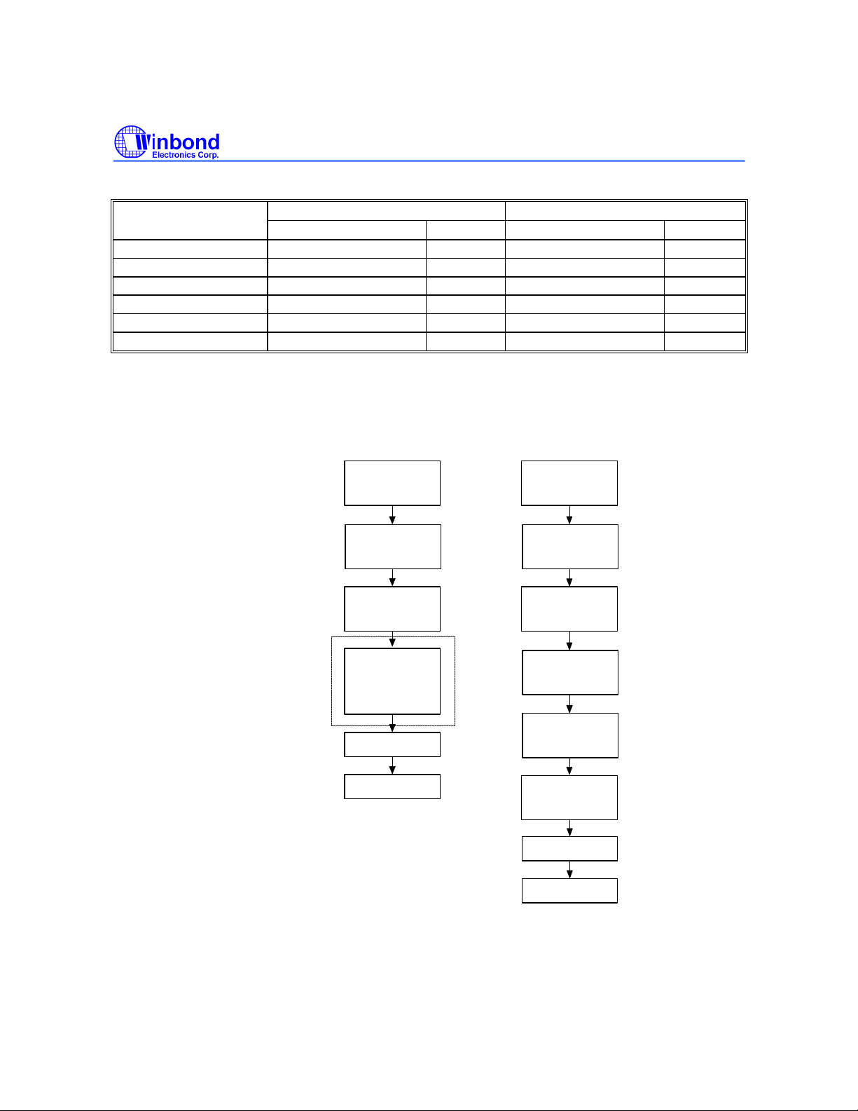
Command Codes for Software Data Protection
BYTE SEQUENCE TO ENABLE PROTECTION TO DISABLE PROTECTION
ADDRESS DATA ADDRESS DATA
0 Write 5555H AAH 5555H AAH
1 Write 2AAAH 55H 2AAAH 55H
2 Write 5555H A0H 5555H 80H
3 Write - - 5555H AAH
4 Write - - 2AAAH 55H
5 Write - - 5555H 20H
Software Data Protection Acquisition Flow
(Optional page-load
operation)
Software Data Protection
Enable Flow
Load data AA
to
address 5555
Load data 55
to
address 2AAA
Load data A0
to
address 5555
Sequentially load
up to 128 bytes
of page data
Pause 10 mS
Exit
Software Data Protection
Disable Flow
Load data AA
to
address 5555
Load data 55
to
address 2AAA
Load data 80
to
address 5555
Load data AA
to
address 5555
Load data 55
to
address 2AAA
Load data 20
to
address 5555
Notes for software program code:
Data Format: DQ7−DQ0 (Hex)
Address Format: A14−A0 (Hex)
Pause 10 mS
Exit
- 6 -
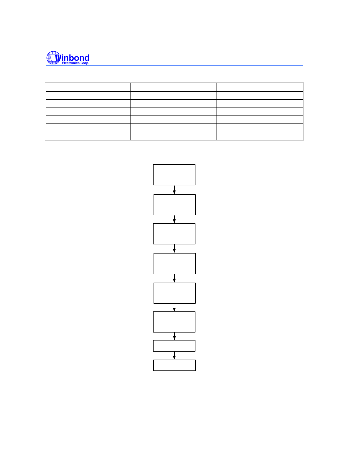
Command Codes for Software Chip Erase
BYTE SEQUENCE ADDRESS DATA
0 Write 5555H AAH
1 Write 2AAAH 55H
2 Write 5555H 80H
3 Write 5555H AAH
4 Write 2AAAH 55H
5 Write 5555H 10H
Software Chip Erase Acquisition Flow
Load data AA
address 5555
Load data 55
address 2AAA
W29C020
to
to
Notes for software chip erase:
Data Format: DQ7−DQ0 (Hex)
Address Format: A14−A0 (Hex)
Load data 80
to
address 5555
Load data AA
to
address 5555
Load data 55
to
address 2AAA
Load data 10
to
address 5555
Pause 50 mS
Exit
Publication Release Date: February 1998
- 7 - Revision A3
 Loading...