

White Electronic Designs EDI9LC644V2012BC, EDI9LC644V2010BC, EDI9LC644V1612BC, EDI9LC644V1610BC, EDI9LC644V1510BC Datasheet
...
128Kx32 SSRAM/1Mx32 SDR AM
EXTERNAL MEMORY SOLUTION FOR TEXAS INSTRUMENTS TMS320C6000 DSP
EDI9LC644V
FEATURES
n Clock speeds:
• SSRAM: 200, 166,150, and 133 MHz
• SDRAMs: 125 and 100 MHz
n DSP Memory Solution
• Texas Instruments TMS320C6201
• Texas Instruments TMS320C6701
n Packaging:
• 153 pin BGA, JEDEC MO-163
n 3.3V Operating supply voltage
n Direct control interface to both the SSRAM and SDRAM
ports on the “C6x”
n Common address and databus
n 65% space savings vs. monolithic solution
n Reduced system inductance and capacitance
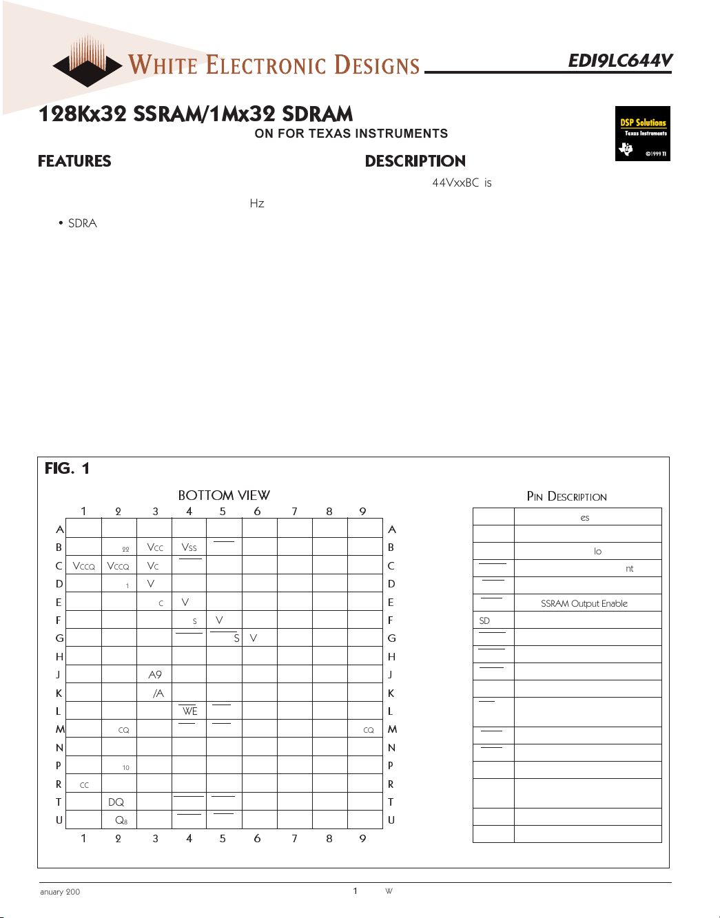
FIG. 1
A
B
C
D
E
F
G
H
J
K
L
M
N
P
R
T
U
PIN CONFIGURATION
BOTTOM VIEW
12 3456 789
DQ19DQ23VCC VSS VSS VSS VCC DQ24DQ28A
DQ18DQ22VCC VSS SDCE VSS VCC DQ25DQ29B
VCCQ VCCQ VCC SDWE SDA10NC VCC VCCQ VCCQ
DQ17DQ21VCC VSS VSS VSS VCC DQ26DQ30D
DQ16DQ20VCC VSS SDCLK VSS VCC DQ27DQ31E
VCCQ VCCQ VCC VSS VSS VSS VCC VCCQ VCCQ
NC NC NC SDRAS SDCAS VSS A2A4A5G
NC NC A8VSS VSS NC A1A3A10H
A6 A7 A9 VSS VSS NC A0 A11 A12
NC/A17 NC/A18NC/A19VSS VSS NC NC A13A14K
NC NC NC BWE2BWE3NC NC A15A16L
VCCQ VCCQ VCC BWE0BWE1NC VCC VCCQ VCCQ
DQ12DQ11VCC VSS VSS VSS VCC DQ4DQ0N
DQ13DQ10VCC VSS SSCLK VSS VCC DQ5DQ1P
VCCQ VCCQ VCC VSS VSS VSS VCC VCCQ VCCQ
DQ14DQ9VCC SSADC SSWE NC VCC DQ6DQ2T
DQ15DQ8VCC SSOE SSCE NC VCC DQ7DQ3U
12 3456 789
DESCRIPTION
The EDI9LC644VxxBC is a 3.3V, 128K x 32 Synchronous
Pipeline SRAM and a 1Mx32 Synchronous DRAM array constructed with one 128K x 32 SBSRAM and two 1Mx16
SDRAM die mounted on a multilayer laminate substrate. The
device is packaged in a 153 lead, 14mm by 22mm, BGA.
The EDI9LC644VxxBC provides a total memory solution for
the Texas Instruments TMS320C6201 and the
TMS320C6701 DSPs
The Synchronous Pipeline SRAM is available with clock
speeds of 200, 166,150, and 133 MHz, allowing the user
to develop a fast external memory for the SSRAM interface port .
The SDRAM is available in clock speeds of 125 and 100
MHz, allowing the user to develop a fast external memory
for the SDRAM interface por t .
PIN D
ESCRIPTION
A0-16 Address Bus
DQ0-31 Data Bus
SSCLK SSRAM Clock
C
F
J
M
R
SSADC S SRAM Address Status Control
SSWE SSRAM Write Enable
SSOE SSRAM Output Enable
SDCLK SDRAM Clock
SDRAS SDRAM Row Address Strobe
SDCAS SDRAM Column Address Strobe
SDWE SDRAM Write Enable
SDA10 SDRAM Address 10/auto precharge
0-3 SSRAM Byte Write Enables
BWE
SSCE Chip Enable SSRAM Device
SDCE Chip Enable SDRAM Device
VCC Power Supply pins, 3.3V
CCQ Data Bus Power Supply pins,
V
VSS Ground
NC No Connect
SDRAM SDQM 0 - 3
3.3V (2.5V future)
January 2002 Rev. 4
ECO# 14667
1
White Electronic Designs Corporation • (602) 437-1520 • www.whiteedc.com
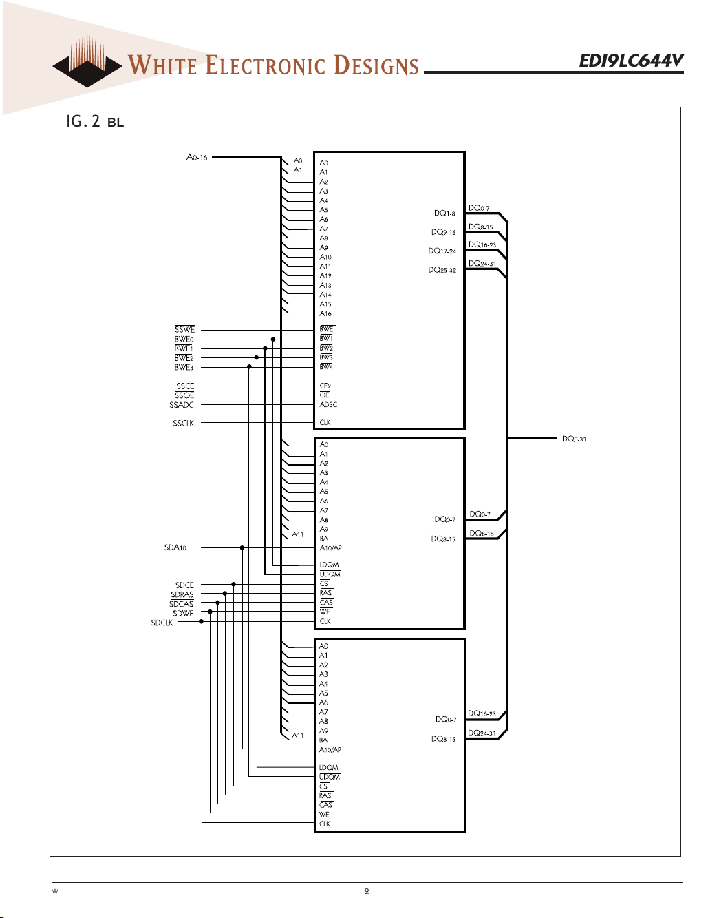
FIG. 2 BLOCK DIAGRAM
EDI9LC644V
White Electronic Designs Corporation • Phoenix AZ • (602) 437-1520
2
EDI9LC644V
OUTPUT FUNCTIONAL DESCRIPTIONS
Symbol Type Signal Polarity Function
SSCLK Input Pulse Positive Edge The system clock input. All of the SSRAM inputs are sampled on the rising edge of the clock.
SSADS When sampled at the positive rising edge of the clock, SSADS, SSOE, and SSWE define the operation
SSOE Input Pulse Active Low to be executed by the SSRAM.
SSWE
SSCE Input Pulse Active Low SSCE disable or enable SSRAM device operation.
SDCLK Input Pulse Positive Edge The system clock input. All of the SDRAM inputs are sampled on the rising edge of the clock.
SDCE Input Pulse Active Low SDCE disable or enable device operation by masking or enabling all inputs except SDCLK and BWE0-3.
SDRAS When sampled at the positive rising edge of the clock, SDCAS, SDRAS, and SDWE define the
SDCAS Input Pulse Active Low operation to be executed by the SDRAM.
SDWE
Address bus for SSRAM and SDRAM
A0 and A1 are the burst address inputs for the SSRAM
During a Bank Active command cycle, A
at the rising clock edge.
A
, Input Level — During a Read or Write command cycle, A
0-16
SDA
10
the rising clock edge. In addition to the row address, SDA10 is used to invoke Autoprecharge
operation at the end of the Burst Read or Write Cycle. If SDA
A
defines the bank to be precharged (low = bank A, high = bank B). If SDA10 is low,
11
autoprecharge is disabled.
During a Precharge command cycle, SDA
to precharge. If SDA
is high, both bank A and Bank B will be precharged regardless of the state of
10
A11. If SDA10 is low, then A11 is used to define which bank to precharge.
DQ
Input Level — Data Input/Output are multiplexed on the same pins.
0-31
Output
BWE
Input Pulse BWE
0-3
perform the byte write enable function for the SSRAM and DQM function for the SDRAM.
0-3
BWE0 is associated with DQ
, BWE1 with DQ
0-7
VCC, VSS Supply Power and ground for the input buffers and the core logic.
VCCQ Supply Data base power supply pins, 3.3V (2.5V future).
, SDA10 defines the row address (RA
0-9
defines the column address (CA
0-7
is high, autoprecharge is selected and
10
is used in conjunction with A11 to control which bank(s)
10
, BWE2 with DQ
8-15
and BWE3 with DQ
16-23
) when sampled
0-10
) when sampled at
0-7
.
24-31
3
White Electronic Designs Corporation • (602) 437-1520 • www.whiteedc.com
EDI9LC644V
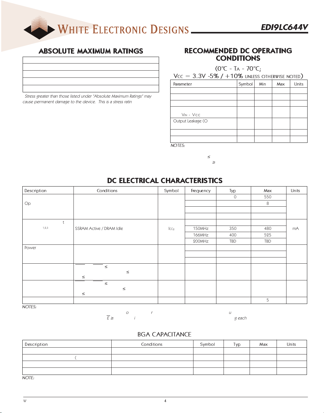
ABSOLUTE MAXIMUM RATINGS
Voltage on Vcc Relative to Vss -0.5V to +4.6V
Vin (DQx) -0.5V to Vcc +0.5V
Storage Temperature (BGA) -55°C to +125°C
Junction Temperature +175°C
Short Circuit Output Current 100 mA
*Stress greater than those listed under "Absolute Maximum Ratings" may
cause permanent damage to the device. This is a stress rating only and
functional operation of the device at these or any other conditions greater
than those indicated in operational sections of this specifications is not
implied. Exposure to absolute maximum rating conditions for extended
periods may affect reliability.
RECOMMENDED DC OPERATING
CONDITIONS
(0°C TA 70°C;
VCC = 3.3V -5% / +10%
Parameter Symbol Min Max Units
Supply Voltage
Input High Voltage
Input Low Voltage
Input Leakage Current IL
0 - VIN - Vcc
Output Leakage (Output Disabled) IL
0 - VIN - Vcc
Output High (IOH = -4mA)
Output Low (I
1
1,2
1,2
OL = 8mA)
1
1
UNLESS OTHERWISE NOTED
VCC 3.135 3.6 V
VIH 2.0 VCC +0.3 V
VIL -0.3 0.8 V
I -10 10 µA
O -10 10 µA
VOH 2.4 — V
VOL — 0.4 V
NOTES:
1. All voltages referenced to Vss (GND).
2. Overshoot: V
Underershoot: V
IH
£
+6.0V for t - tKC/2
IL
³
-2.0V for t - tKC/2
DC ELECTRICAL CHAR ACTERISTICS
Description Conditions Symbol Frequency Typ Max Units
Power Supply Current: 133MHz 400 550
Operating (1,2,3) SSRAM Active / DR AM Auto Refresh ICC
Power Supply Current 133MHz 300 450
1,2,3
Operating
Power Supply Current 83MHz 220 240
1,2,3
Operating
SSRAM Active / DRAM Idle ICC
SDRAM Active / SSRAM Idle ICC
SSCE and SDCE £ V
CC -0.2V, ISB
1
2
3
1
CMOS Standby All other inputs at VSS +0.2 £ VIN or mA
VIN £ VCC -0.2V, Clk frequency = 0
SSCE and SDCE £ V
IH min ISB
2
TTL Standby All other inputs at VIL max £ VIN or mA
VIN £ VCC -0.2V, Clk frequency = 0
Auto Refresh I
CC
5
NOTES:
1. ICC (operating) is specified with no output current. ICC (operating) increases with faster cycle times and greater output loading.
2. “Device idle” means device is deselected (CE
3. Typical values are measured at 3.3V, 25°C. I
³
VIH) Clock is running at max frequency and Addresses are switching each cycle.
CC (operating) is specified at specified frequency.
150MHz 450 580 mA
166MHz 500 625
200MHz TBD TBD
150MHz 350 480 mA
166MHz 400 525
200MHz TBD TBD
100MHz 235 250 mA
125MHz 255 280
20.0 40.0
30.0 55.0
190 250 mA
)
BGA CAPACITANCE
Description Conditions Symbol Typ Max Units
Address Input Capacitance
Input/Output Capacitance (DQ)
Control Input Capacitance
Clock Input Capacitance
NOTE:
1. This parameter is sampled.
White Electronic Designs Corporation • Phoenix AZ • (602) 437-1520
1
1
1
1
TA = 25°C; f = 1MHz CI 58pF
TA = 25°C; f = 1MHz CO 810pF
TA = 25°C; f = 1MHz CA 58 pF
TA = 25°C; f = 1MHz CCK 46pF
4
EDI9LC644V
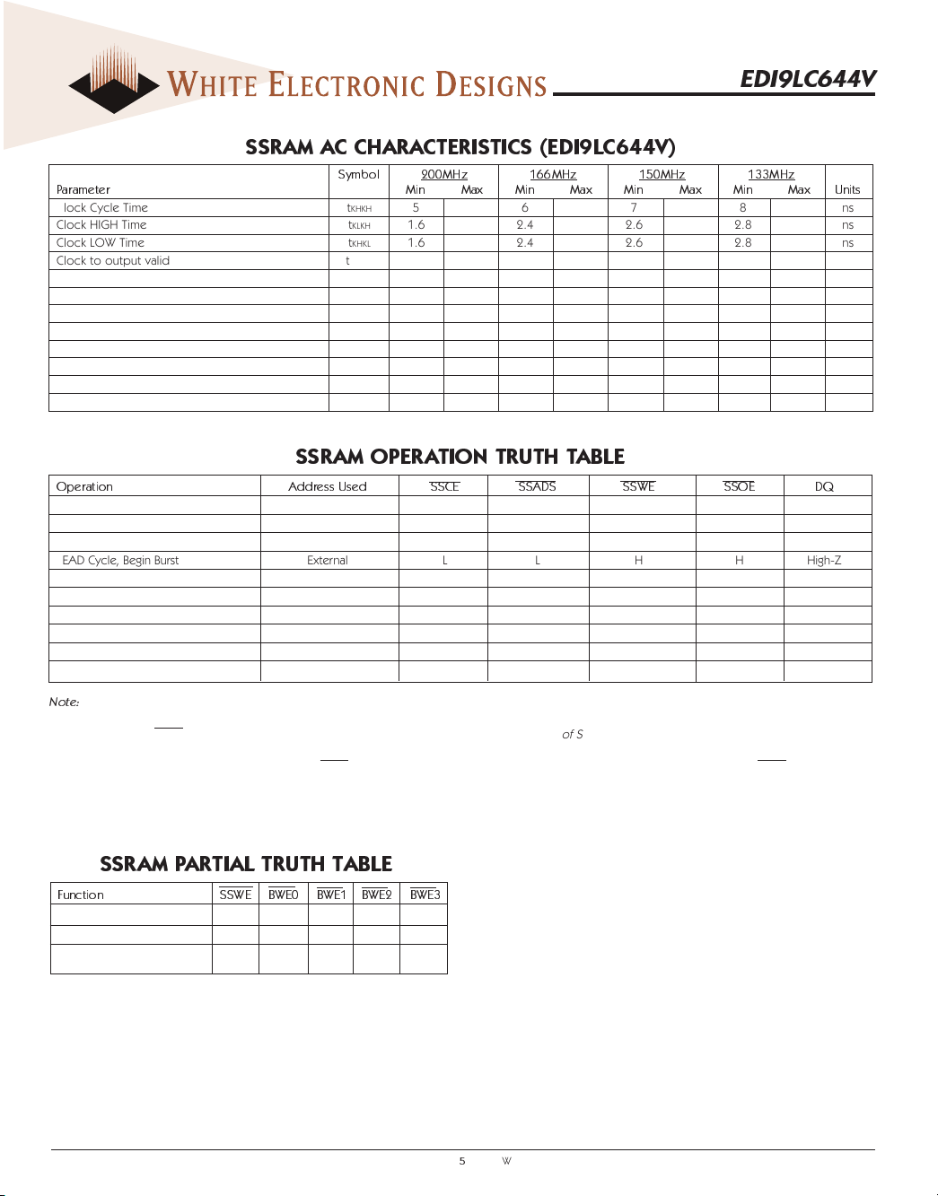
SSRAM AC CHARACTERISTICS (EDI9LC644V)
Parameter Min Max Min Max Min Max Min Max Units
Clock Cycle Time tKHKH 5678ns
Clock HIGH Time tKLKH 1.6 2.4 2.6 2.8 ns
Clock LOW Time tKHKL 1.6 2.4 2.6 2.8 ns
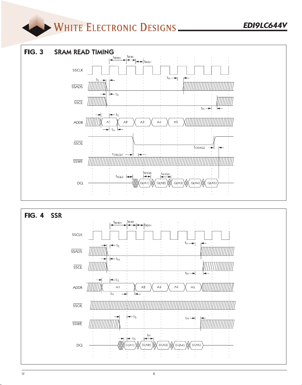
Clock to output valid tKHQV 2.5 3.5 3.8 4.0 ns
Clock to output invalid tKHQX 1.5 1.5 1.5 1.5 ns
Clock to output on Low-Z tKQLZ 0000ns
Clock to output in High-Z tKQHZ 1.5 3 1.5 3.5 1.5 3.8 1.5 4.0 ns
Output Enable to output valid tOELQV 2.5 3.5 3.8 4.0 ns
Output Enable to output in Low-Z tOELZ 0000ns
Output Enable to output in High-Z tOEHZ 3.0 3.5 3.5 3.8 ns
Address, Control, Data-in Setup Time to Clock tS 1.5 1.5 1.5 1.5 ns
Address, Control, Data-in Hold Time to Clock t
Operation Address Used SSCE SSADS SSWE SSOE DQ
Deselected Cycle, Power Down None H L X X High-Z
WRITE Cycle, Begin Burst External L L L X D
READ Cycle, Begin Burst External L L H L Q
READ Cycle, Begin Burst External L L H H High-Z
READ Cycle, Suspend Burst Current X H H L Q
READ Cycle, Suspend Burst Current X H H H High-Z
READ Cycle, Suspend Burst Current H H H L Q
READ Cycle, Suspend Burst Current H H H H High-Z
WRITE Cycle, Suspend Burst Current X H L X D
WRITE Cycle, Suspend Burst Current H H L X D
Symbol 200MHz 166MHz 150MHz 133MHz
H 0.5 0.5 0.5 0.5 ns
SSRAM OPERATION TRUTH TABLE
Note:
1. X means “don’t care”, H means logic HIGH. L means logic LOW.
2. All inputs except SSOE must meet setup and hold times around the rising edge (LOW to HIGH) of SSCLK.
3. Suspending burst generates wait cycle
4. For a write operation following a read operation, SSOE must be HIGH before the input data required setup time plus High-Z time for SSOE and staying
HIGH though out the input data hold time.
5. This device contains circuitry that will ensure the outputs will be in High-Z during power-up.
SSRAM PARTIAL TRUTH TABLE
Function SSWE BWE0 BWE1 BWE2 BWE3
READ H X X X X
WRITE one Byte (DQ
WRITE all Bytes L L L L L
)LLHHH
0-7
5
White Electronic Designs Corporation • (602) 437-1520 • www.whiteedc.com
EDI9LC644V
FIG. 3
FIG. 4
SSRAM READ TIMING
SSRAM WRITE TIMING
White Electronic Designs Corporation • Phoenix AZ • (602) 437-1520
6
EDI9LC644V
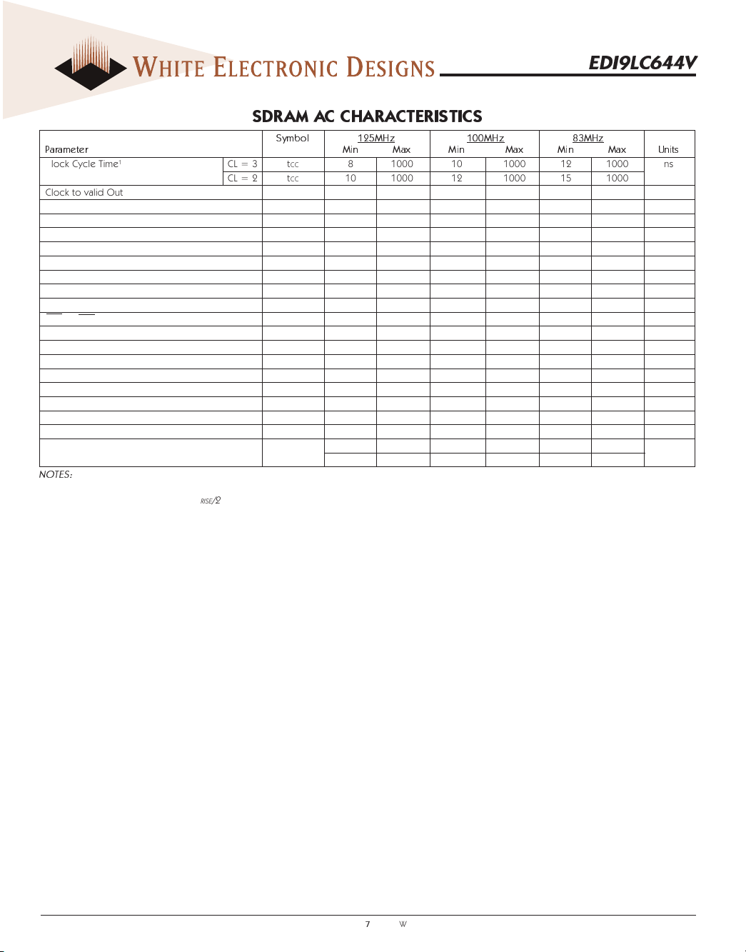
SDRAM AC CHARACTERISTICS
Parameter Min Max Min Max Min Max Units
Clock Cycle Time
Clock to valid Output delay
Output Data Hold Time
Clock HIGH Pulse Width
Clock LOW Pulse Width
Input Setup Time
Input Hold Time
CLK to Output Low-Z
CLK to Output High-Z tSHZ 778ns
Row Active to Row Active Delay
RAS to CAS Delay
Row Precharge Time
Row Active Time
Row Cycle Time - Operation
Row Cycle Time - Auto Refresh
Last Data in to New Column Address Delay
Last Data in to Row Precharge
Last Data in to Burst Stop
Column Address to Column Address Delay
Number of Valid Output Data
1
1,2
2
3
3
3
3
2
4
4
4
4
4,8
5
5
7
CL = 3 tCC 8 1000 10 1000 12 1000 ns
CL = 2 tCC 10 1000 12 1000 15 1000
4
5
6
NOTES:
1. Parameters depend on programmed CAS latency.
2. If clock rise time is longer than 1ns (t
3. Assumed input rise and fall time = 1ns. If t
RISE/2 -0.5)ns should be added to the parameter.
RISE of tFALL are longer than 1ns. [(tRISE = tFALL)/2] - 1ns should be added to the parameter.
4. The minimum number of clock cycles required is detemined by dividing the minimum time required by the clock cycle time and then rounding up to the
next higher integer.
5. Minimum delay is required to complete write.
6. All devices allow every cycle column address changes.
7. In case of row precharge interrupt, auto precharge and read burst stop.
8. A new command may be given t
RFC after self-refresh exit.
Symbol 125MHz 100MHz 83MHz
tSAC 678ns
tOH 33 3ns
tCH 33 3ns
tCL 33 3ns
tSS 22 2ns
tSH 11 1ns
tSLZ 22 2ns
tRRD 20 20 24 ns
tRCD 20 20 24 ns
tRP 20 20 24 ns
tRAS 50 10,000 50 10,000 60 10,000 ns
tRC 70 80 90 ns
tRFC 70 80 90 ns
tCDL 1 1 1 CLK
tRDL 1 1 1 CLK
tBDL 1 1 1 CLK
tCCD 1.5 1.5 1.5 CLK
22 2
12 1
ea
7
White Electronic Designs Corporation • (602) 437-1520 • www.whiteedc.com
EDI9LC644V
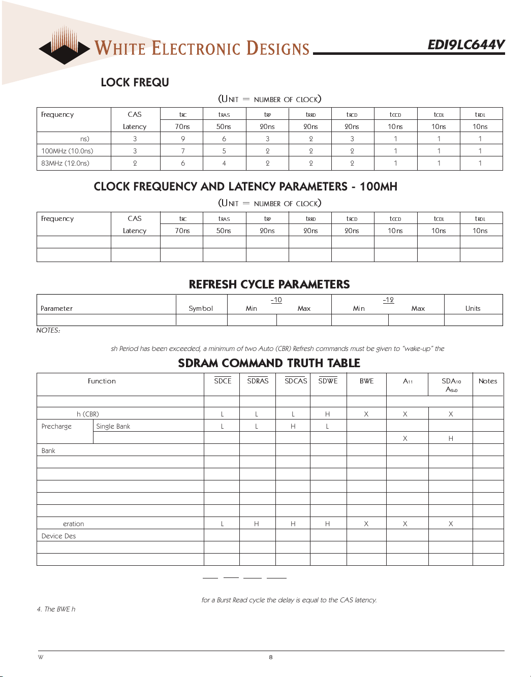
CLOCK FREQUENCY AND LATENCY PARAMETERS - 125MHZ SDRAM
(U
NIT
=
NUMBER OF CLOCK
Frequency CAS t
RC
t
RAS
t
RP
Latency 70ns 50ns 20ns 20ns 20ns 10ns 10ns 10ns
125MHz (8.0ns) 3 9 6 3 2 3 1 1 1
100MHz (10.0ns) 3 7 5 2 2 2 1 1 1
83MHz (12.0ns) 2 6 4 2 2 2 1 1 1
CLOCK FREQUENCY AND LATENCY PARAMETERS - 100MHZ SDRAM
(U
NIT
=
NUMBER OF CLOCK
Frequency CAS t
RC
t
RAS
t
RP
Latency 70ns 50ns 20ns 20ns 20ns 10ns 10ns 10ns
100MHz (12.0ns) 3 7 5 2 2 2 1 1 1
83MHz (12.0ns) 2 6 5 2 2 2 1 1 1
REFRESH CYCLE PARAMETERS
Parameter Symbol Min Max Min Max Units
Refresh Period
1,2
tREF —64 — 64 ms
NOTES:
1. 4096 cycles
2. Any time that the Refresh Period has been exceeded, a minimum of two Auto (CBR) Refresh commands must be given to “wake-up” the device.
-10 -12
SDRAM COMMAND TRUTH TABLE
Function SDCE SDRAS SDCAS SDWE BWE A
Mode Register Set L L L L X OP CODE
Auto Refresh (CBR) L L L H X X X
Precharge Single Bank L L H L X BA L 2
Precharge all Banks L L H L X X H
Bank Activate L L H H X BA Row Address 2
Write L H L L X BA L 2
Write with Auto Precharge L H L L X BA H 2
Read L H L L X BA L 2
Read with Auto Precharge L H L H X BA H 2
Burst Termination L H H L X X X 3
No Operation L H H H X X X
Device Deselect H X X X X X X
Data Write/Output Disable X X X X L X X 4
Data Mask/Output Disable X X X X H X X 4
NOTES:
1. All of the SDRAM operations are defined by states of SDCE, SDWE, SDRAS, SDC AS, and BWE
2. Bank Select (BA), if A
3. During a Burst Write cycle there is a zero clock delay, for a Burst Read cycle the delay is equal to the CAS latency.
4. The BWE has two functions for the data DQ Read and Write operations. During a Read cycle, when BWE goes high at a clock timing the data outputs are
disabled and become high impedance after a two clock delay. BWE also provides a data mask function for Write cycles. When it activates, the Write
operation at the clock is prohibited (zero clock latency).
= 0 then bank A is selected, if BA = 1 then bank B is selected.
11
)
t
RRD
t
RCD
t
CCD
)
t
RRD
t
RCD
at the positive rising edge of the clock.
0-3
t
CCD
t
CDL
t
CDL
11
SDA
t
RDL
t
RDL
Notes
10
A
9-0
White Electronic Designs Corporation • Phoenix AZ • (602) 437-1520
8
 Loading...