

Western Digital HUS726T6TALE6L4, HUS726T6TALN6L4, HUS726T4TALE6L4, HUS726T4TALN6L4, HUS726T4TALA6L4 User Manual
Page 1

Models:
HUS726T6TALE6L4
HUS726T6TALN6L4
HUS726T4TALE6L4
HUS726T4TALN6L4
HUS726T4TALA6L4
Hard Disk Drive Specifications
Ultrastar™ DC HC310
3.5 inch Serial ATA Hard Disk Drive
Revision 1.4
18 September 2018
Page 2

Publication Disclaimer Information
One MB is equal to one million bytes, one GB is equal to one billion bytes and one TB equals 1,000GB (one trillion
bytes) when referring to storage capacity. Accessible capacity will vary from the stated capacity due to formatting and
partitioning of the drive, the computer’s operating system, and other factors.
The following paragraph does not apply to any jurisdiction where such provisions are inconsistent with local law: THIS
PUBLICATION IS PROVIDED "AS IS" WITHOUT WARRANTY OF ANY KIND, EITHER EXPRESS OR IMPLIED,
INCLUDING, BUT NOT LIMITED TO, THE IMPLIED WARRANTIES OF MERCHANTABILITY OR FITNESS FOR A
PARTICULAR PURPOSE.
This publication could include technical inaccuracies or typographical errors. Changes are periodically made to the
information herein; these changes will be incorporated in new editions of the publication. There may be improvements or
changes in any products or programs described in this publication at any time. It is possible that this publication may
contain reference to, or information about, Western Digital products (machines and programs), programming, or services
that are not announced in your country. Such references or information must not be construed to mean that Western
Digital Corporation intends to announce such Western Digital products, programming, or services in your country.
Technical information about this product is available by contacting your local Western Digital product representative or
on the Internet at: support@wdc.com.
Western Digital Corporation may have patents or pending patent applications covering subject matter in this document.
The furnishing of this document does not give you any license to these patents.
© 2017 Western Digital Corporation or its affiliates.
Western Digital and Ultrastar are registered trademarks or trademarks of Western Digital Corporation or its affiliates in
the U.S. and/or other countries. All other marks are the property of their respective owners.
References in this publication to Western Digital-branded products, programs, or services do not imply that they will be
made available in all countries. Product specifications provided are sample specifications and do not constitute a
warranty. Actual specifications for unique part numbers may vary. Please visit the Support section of our website,
support@wdc.com, for additional information on product specifications. Pictures shown may vary from actual products.
Page 3

Table of Contents
1 General ................................................................................................ ........................................... 1
1.1 Introduction.......................................................................................................................... 1
1.2 Glossary ............................................................................................................................... 2
1.3 General Caution ................................................................................................................... 2
1.4 References ............................................................................................................................ 2
2 General Features ................................ .............................................................................................. 3
Part 1. Functional Specification ............................................................................................................. 4
3 Fixed Disk Subsystem Description ....................................................................................................... 5
3.1 Contr ol Electronics ............................................................................................................... 5
3.2 Head Disk Assembly ............................................................................................................. 5
3.3 Actuator ............................................................................................................................... 5
4 Drive Characteristics.......................................................................................................................... 6
4.1 Default Logical Drive Parameters ......................................................................................... 6
4.2 Data Sheet............................................................................................................................ 7
4.3 World Wide Name Assignment .............................................................................................. 7
4.4 Drive Organization ............................................................................................................... 8
4.4.1 Drive Format ................................................................................................................. 8
4.4.2 Cylinder Allocation ......................................................................................................... 8
4.5 Performance Characteristics ................................................................................................. 9
4.5.1 Mechanical Positioning ................................................................................................... 9
4.5.2 Drive Ready Time..........................................................................................................10
4.5.3 Operating Modes ...........................................................................................................10
5 Defect Flagging Strategy ...................................................................................................................12
5.1 Shipped Format ...................................................................................................................12
6 Specification................................................................................................ ....................................13
6.1 Electrical Interface ..............................................................................................................13
6.1.1 Conn ector Location........................................................................................................13
6.1.2 Signal Definition (SATA) ...............................................................................................15
6.1.3 Out of Ban d Signaling (SATA) .......................................................................................16
6.1.4 Voltage and Ground Signals...........................................................................................16
6.1.5 Ready LED Output........................................................................................................16
6.2 Environment........................................................................................................................17
6.2.1 Temperature and Humidity ...........................................................................................17
6.2.2 Storage Requirements ...................................................................................................18
6.2.3 Corrosion Test ...............................................................................................................18
6.2.4 Atmospheric Condition ..................................................................................................18
6.3 DC Power Requirements ......................................................................................................19
6.3.1 Input Voltage ................................................................................................................19
6.3.2 Power Supply Current ...................................................................................................21
6.3.3 Power Line Noise Limits................................................................................................24
6.3.4 Power Consumption Efficiency.......................................................................................24
6.4 Reliability ............................................................................................................................25
6.4.1 Data Integrity ...............................................................................................................25
6.4.2 Cable Noise Interference ...............................................................................................25
6.4.3 Load/Unload..................................................................................................................25
6.4.4 Start/Stop Cycles ...........................................................................................................25
6.4.5 Preventive Maintenance ................................................................................................25
6.4.6 Data Reliability .............................................................................................................25
6.5 Mechanical Specifications ....................................................................................................26
6.5.1 Physical Dimensions......................................................................................................26
6.5.2 Drive Moun ting .............................................................................................................27
Page 4

6.5.3 Heads Unload and Actuator Lock...................................................................................27
6.6 Vibration and Shock.............................................................................................................28
6.6.1 Operating Vibration ......................................................................................................28
6.6.2 Nonoperating Vibration .................................................................................................29
6.6.3 Operating Shock ............................................................................................................29
6.6.4 Nonoperating Shock ......................................................................................................29
6.6.5 Nonoperating Rotational Shock .....................................................................................30
6.7 Acoustics .............................................................................................................................31
6.8 Identification Labels ............................................................................................................31
6.9 Safety ..................................................................................................................................32
6.9.1 UL and CSA Standard Conformity .................................................................................32
6.9.2 European Safety Mark ..................................................................................................32
Flammability ................................................................................................................32
6.9.3
6.9.4 Safe Handling ...............................................................................................................32
Substance Restriction Requirem ents ..............................................................................32
6.9.5
6.9.6 Secondary Circuit Protection .........................................................................................32
6.10 Electromagnetic Compatibility ..........................................................................................33
6.10.1 CE Mark .......................................................................................................................33
6.10.2 RCM Mark ....................................................................................................................33
6.10.3 BSMI Mark ...................................................................................................................33
6.10.4 KC Mark .......................................................................................................................34
6.11 Third Party Notices ..........................................................................................................34
Part 2. Interface Specification...............................................................................................................35
7 General ................................................................................................ ..........................................36
7.1 Introduction.........................................................................................................................36
7.2 Terminology .........................................................................................................................36
7.3 Deviations From Standard ...................................................................................................36
8 Registers ................................................................................................ ........................................37
8.1 Alternate Status Register.....................................................................................................37
8.2 Command Register ..............................................................................................................37
8.3 Cylinder High Register ........................................................................................................37
8.4 Cylinder Low Register..........................................................................................................38
8.5 Device Control Register........................................................................................................38
8.6 Device/Head Register ...........................................................................................................38
8.7 Error Register......................................................................................................................39
8.8 Features Register ................................................................................................................39
8.9 Sector Count Register ..........................................................................................................39
8.10 Sector Number Register ....................................................................................................39
8.11 Status Register .................................................................................................................40
9 General Operation Descriptions..........................................................................................................41
9.1 Reset Response ....................................................................................................................41
9.1.1 Register Initialization....................................................................................................42
9.2 Diagnostic and Reset Considerations ....................................................................................42
9.3 Sector Addressing Mode .......................................................................................................43
9.3.1 Logical CHS Addressing Mode .......................................................................................43
9.3.2 LBA Addr essing Mode ...................................................................................................43
9.4 Power Management Feature ................................................................................................44
9.4.1 Power Mode ..................................................................................................................44
9.4.2 Power Management Commands .....................................................................................45
9.4.3 Standby Timer ..............................................................................................................45
9.4.4 Interface Capability for Power Modes ............................................................................45
9.5 SMART Function .................................................................................................................46
9.5.1 Attributes .....................................................................................................................46
9.5.2 Attribute Values ............................................................................................................46
Page 5

9.5.3 Attribute Thresholds .....................................................................................................46
9.5.4 Threshold Exceeded Condition .......................................................................................46
9.5.5 SMART Commands .......................................................................................................46
9.5.6 Off-Line Read Scanning .................................................................................................46
9.5.7 Error Log ......................................................................................................................47
9.5.8 Self-Test ........................................................................................................................47
9.6 Security Mode Feature Set ...................................................................................................48
9.6.1 Security Mode ...............................................................................................................48
9.6.2 Security Level ...............................................................................................................48
9.6.3 Password.......................................................................................................................48
9.6.4 Operation Example .......................................................................................................49
9.6.5 Command Table ............................................................................................................52
Host Protected Area Feature ................................................................................................55
9.7
9.7.1 Example for Operation (in LBA mode)............................................................................55
Security Extensions.......................................................................................................56
9.7.2
9.8 Write Cache Function ..........................................................................................................57
9.9 Reassign Function ...............................................................................................................57
9.9.1 Auto Reassign Function.................................................................................................57
9.10 Power-Up in Standby Feature Set .....................................................................................58
9.11 Advanc ed Power Management Feature Set (APM).............................................................58
9.12 48-bit Address Feature Set................................................................................................58
9.13 Streaming Feature Set......................................................................................................59
9.13.1 Streaming Commands ...................................................................................................59
9.14 SATA BIST (built-in self-test)............................................................................................61
9.15 SATA Interface Power Management ..................................................................................62
9.15.1 Low PHY Power Conditions Overview............................................................................62
9.15.2 Active PHY Power Condition .........................................................................................62
9.15.3 Partial PHY Power Condition ........................................................................................62
9.15.4 Slumber PHY Power Condition ......................................................................................62
9.16 Software Setting Preservation ..........................................................................................63
9.16.1 COMRESET Preservation Requirements .......................................................................63
9.17 Serial ATA Optional Features............................................................................................64
9.17.1 Asynchronous Signal Recovery ......................................................................................64
9.17.2 Device Power Connector Pin 11 Definition......................................................................64
9.17.3 Phy Event Counters ......................................................................................................64
9.17.4 NCQ NON-DATA (63h) ..................................................................................................69
9.17.5 Rebuild Assist ...............................................................................................................73
9.17.6 Power Disable ...............................................................................................................74
9.18 SCT Command Transport Feature Set ..............................................................................75
9.18.1 Overview.......................................................................................................................75
9.18.2 SCT Command Protocol .................................................................................................77
9.18.3 SCT Command Set ........................................................................................................85
9.19 Exten ded Power Conditions (EPC) Feature .......................................................................93
9.19.1 Power Conditions ..........................................................................................................93
9.19.2 Power Condition Timers ................................................................................................94
9.19.3 Interaction with Resets, Commands and other Features.................................................94
9.20 Sanitize Device Feature Set ..............................................................................................95
9.20.1 Overview.......................................................................................................................95
9.20.2 Sanitize Device Feature.................................................................................................96
9.20.3 Sanitize Device State Machine.......................................................................................97
9.21 Trusted Computing Group Feature Set..............................................................................99
9.21.1 Referenced Specifications and Standards .......................................................................99
9.21.2 Implementation Exceptions ......................................................................................... 100
9.21.3 Implementation Features and Details Outside of TCG Specifications ........................... 100
Page 6

9.21.4 Encryption Algorithms ................................................................................................ 101
9.21.5 TCG Enterprise SSC Tables......................................................................................... 102
9.21.6 Firmware Download and Signing ................................................................................. 105
9.21.7 Ports ........................................................................................................................... 105
9.21.8 MSID .......................................................................................................................... 108
9.21.9 Logging ....................................................................................................................... 108
9.21.10 Number of Sessions .................................................................................................. 108
9.21.11 Number of Bands ..................................................................................................... 108
9.21.12 Number of COMIDs ................................................................................................. 108
9.21.13 PSID........................................................................................................................ 108
9.21.14 Locked and Unlocked Behavior................................................................................. 109
9.21.15 Error Codes.............................................................................................................. 114
9.21.16
9.21.17 Customer Specific Requirements .............................................................................. 114
Command Protocol......................................................................................................................... 115
10
10.1 PIO Data In commands................................................................................................... 115
10.2
10.3 Non-Data commands ...................................................................................................... 116
10.4 DMA Data In commands and DMA Data Out commands ................................................. 117
10.5 First-party DMA commands ............................................................................................ 117
11 Command Descriptions ................................ ................................................................ ................... 118
11.1 Check Power Mode (E5h/98h).......................................................................................... 123
11.2 Configure Stream (51h)................................................................................................... 124
11.3 Device Configuration Overlay (B1h) ................................................................................ 126
11.3.1
11.3.2 Device Configuration Freeze Lock (Subcommand C1h) ................................................. 127
11.3.3 Device Configuration Identify (Subcommand C2h) ....................................................... 127
11.3.4 Device Configuration Set (Subcommand C3h) .............................................................. 127
11.4 Download Microcode (92h) .............................................................................................. 130
11.5 Download Microcode DMA (93h)...................................................................................... 132
11.6 Execute Device Diagnostic (90h) ..................................................................................... 134
11.7 Flush Cache (E7h) .......................................................................................................... 135
11.8 Flush Cache Ext (EAh) ................................................................................................... 136
11.9 Format Track (50h)......................................................................................................... 137
11.10 Format Unit (F7h) .......................................................................................................... 138
11.11 Identify Device (ECh)...................................................................................................... 139
11.12 Idle (E3h/97h)................................................................................................................. 150
11.13 Idle Immediate (E1h/95h) ............................................................................................... 151
11.14 Initialize Device Parameters (91h) .................................................................................. 152
11.15 NCQ NON-DATA (63h) ................................................................................................... 153
11.15.1 Abort NCQ Queue Subcommand (0h) ........................................................................ 154
11.15.2 Deadline handling Subcommand (1h) ....................................................................... 156
11.15.3 Set Features Subcommand (5h) ................................................................................ 158
11.16 RECEIVE FPDMA QUEUED (65h) ................................................................................. 160
11.16.1 READ LOG DMA EXT (1h)....................................................................................... 161
11.17 SEND FPDMA QUEUED (64h)....................................................................................... 163
11.17.1 WRITE LOG DMA EXT (2h)..................................................................................... 164
11.18 Read Buffer (E4h) ........................................................................................................... 166
11.19 Read Buffer DMA (E9h) .................................................................................................. 167
11.20 Read DMA(C8h/C9h) ...................................................................................................... 168
11.21 Read DMA Ext (25h) ....................................................................................................... 170
11.22 Read FPDMA Queued (60h) ............................................................................................ 172
11.23 Read Log Ext (2Fh)......................................................................................................... 174
11.23.1 General Purpose Log Directory ................................................................................. 176
Life Cycle model....................................................................................................... 114
PIO Data Out commands ................................................................................................ 115
Device Configuration Restore (Subcommand C0h) ........................................................ 127
Page 7

11.23.2 Exten ded Comprehensive SMART Error log ............................................................. 177
11.23.3 Device Statistics log ................................................................................................. 180
11.23.4 Exten ded Self-test log sector..................................................................................... 186
11.23.5 Power Conditions log................................................................................................ 187
11.23.6 Queued Error Log .................................................................................................... 190
11.23.7 Read Stream Error log ............................................................................................. 191
11.23.8 Write Stream Error log............................................................................................. 192
11.23.9 Identify Device Data log ........................................................................................... 193
11.24 Read Log DMA Ext(47h) ................................................................................................. 205
11.25 Read Multiple (C4h) ....................................................................................................... 206
11.26 Read Multiple Ext (29h) .................................................................................................. 207
11.27 Read Native Max Address (F8h) ...................................................................................... 209
Read Native Max Address Ext (27h) ................................................................................ 210
11.28
11.29 Read Sector(s) (20h/21h ) ................................................................................................. 211
Read Sector(s) Ext (24h) ................................................................................................. 212
11.30
11.31 Read Stream DMA Ext(2Ah) ........................................................................................... 213
11.32 Read Stream Ext (2Bh ) ................................................................................................... 216
11.33 Read Verify Sector(s) (40h/41h) ....................................................................................... 219
11.34 Read Verify Sector(s) Ext (42h) ....................................................................................... 220
11.35 Recalibrate (1xh) ............................................................................................................ 221
11.36 Request Sense Data Ext (0Bh) ........................................................................................ 222
11.37 Sanitize Device Feature Set (B4h) ................................................................................... 224
11.37.1 Crypto Scramble Ext Command (feature: 0011h)....................................................... 224
11.37.2 Overwrite Ext Command (feature: 0014h)................................................................. 226
11.37.3 Sanitize Freeze Lock Ext Command (feature: 0020h) ................................................ 228
11.37.4 Sanitize Status Ext Command (feature: 0000h)......................................................... 230
11.38 Security Disable Password (F6h) ..................................................................................... 232
11.39 Security Erase Prepar e (F3h) .......................................................................................... 233
11.40 Security Erase Unit (F4h) ............................................................................................... 234
11.41 Security Freeze Lock (F5h) ............................................................................................. 236
11.42 Security Set Password (F1h) ........................................................................................... 237
11.43 Security Unlock (F2h) ..................................................................................................... 239
11.44 Seek (7xh) ...................................................................................................................... 240
11.45 Sense Condition (F0h : Vendor specific) ........................................................................... 241
11.46 Set Features (EFh) ......................................................................................................... 242
11.46.1 Set Transfer Mode .................................................................................................... 243
11.46.2 Write Cache ............................................................................................................. 243
11.46.3 Serial ATA Feature ................................................................................................... 243
11.46.4 Advanc ed Power Management .................................................................................. 244
11.46.5 Set Maximum Host Interfac e Sector Time................................................................. 244
11.46.6 Extended Power Conditions (EPC) feature ................................................................ 245
11.47 Set Max Address (F9h).................................................................................................... 252
11.47.1 Set Max Set Password (Feature = 01h) ..................................................................... 254
11.47.2 Set Max Lock (Feature = 02h)................................................................................... 255
11.47.3 Set Max Unlock (Feature = 03h) ............................................................................... 256
11.47.4 Set Max Freeze Lock (Feature = 04h)........................................................................ 257
11.48 Set Max Address Ext (37h).............................................................................................. 258
11.49 Set Multiple (C6h) .......................................................................................................... 260
11.50 Sleep (E6h/99h) .............................................................................................................. 261
11.51 SMART Function Set (B0h)............................................................................................. 262
11.51.1 SMART Subcommand .............................................................................................. 263
11.51.2 Device Attributes Data Structure ............................................................................. 267
11.51.3 Device Attribute Thresholds Data Structure ............................................................. 272
11.51.4 SMART Log Directory .............................................................................................. 273
Page 8

11.51.5 SMART summary error log sector ............................................................................. 273
11.51.6 Self-test log data structure ....................................................................................... 275
11.51.7 Selective self-test log data structure ......................................................................... 276
11.51.8 Error Reporting........................................................................................................ 277
11.52 Standby (E2h/96h) .......................................................................................................... 278
11.53 Standby Immediate (E0h/94h) ........................................................................................ 279
11.54 Trusted Receive (5Ch) ..................................................................................................... 280
11.55 Trusted Receive DMA (5Dh) ............................................................................................ 281
11.56 Trusted Send (5Eh) ......................................................................................................... 282
11.57 Trusted Send DMA (5Fh) ................................................................................................ 283
11.58 Write Buffer (E8h) .......................................................................................................... 284
11.59 Write Buffer DMA (EBh) ................................................................................................. 285
Write DMA (CAh/CBh ).................................................................................................... 286
11.60
11.61 Write DMA FUA Ext (3Dh) ............................................................................................. 287
Write DMA Ext (35h) ...................................................................................................... 289
11.62
11.63 Write FPDMA Queued (61h) ........................................................................................... 291
11.64 Write Log Ext (3Fh) ........................................................................................................ 293
11.65 Write Log DMA Ext (57h)................................................................................................ 294
11.66 Write Multiple (C5h)....................................................................................................... 295
11.67 Write Multiple Ext (39h) ................................................................................................. 296
11.68 Write Multiple FUA Ext (CEh) ........................................................................................ 297
11.69 Write Sector(s) (30h/31h) ................................................................................................ 299
11.70 Write Sector(s) Ext (34h)................................................................................................. 300
11.71 Write Stream DMA Ext (3Ah) ......................................................................................... 301
11.72 Write Stream Ext (3Bh) .................................................................................................. 304
11.73 Write Uncorrectable Ext (45h)......................................................................................... 307
Page 9

List of Tables
Table 1 R/N and Model# ................................................................................................................ 1
Table 2 Formatted Capacity .......................................................................................................... 6
Table 3 Data Sheet ....................................................................................................................... 7
Table 4 World Wide Name Assignment .......................................................................................... 7
Table 5 Average Seek Time ........................................................................................................... 9
Table 6 Single Track Seek Time .................................................................................................... 9
Table 7 Latency Time.................................................................................................................... 9
Table 8 Drive Ready Time ............................................................................................................10
Table 9 6TB Mode Transition Times ............................................................................................. 11
Table 10 4TB Mode Transition Times ........................................................................................... 11
Table 11 Interface Connector Pins and I/O Signals .......................................................................15
Table 12 Parameter Descriptions .................................................................................................16
Table 13 Temper ature and Humidity............................................................................................17
Table 14 Input Voltage .................................................................................................................19
Table 15 SATA Power Consumption, 6TB, 4k................................................................................21
Table 16 SATA Power Consumption, 4TB, 4k................................................................................22
Table 17 SATA Power Consumption, 4TB, 512n ............................................................................23
Table 18 Allowable Power Supply Noise Limits at Drive Power Connector ....................................24
Table 19 Power Consumption Efficiency .......................................................................................24
Table 20 Physical Dimensions ......................................................................................................26
Table 21 Random Vibration PSD Profile Break Points (operating).................................................28
Table 22 Random Vibration (Rotational) PSD Profile Break Points ...............................................28
Table 23 Random Vibration PSD Profile Break Points (non operating) ...........................................29
Table 24 Sinusoidal Shock Wave ..................................................................................................30
Table 25 Rotational Shock............................................................................................................30
Table 26 Sound Power Levels .......................................................................................................31
Table 27 Alternate Status Register ..............................................................................................37
Table 28 Device Control Register .................................................................................................38
Table 29 Device/Head Register .....................................................................................................38
Table 30 Error Register ...............................................................................................................39
Table 31 Status Register ..............................................................................................................40
Table 32 Reset Respons e ..............................................................................................................41
Table 33 Default Register Values .................................................................................................42
Table 34 Diagnostic Codes ...........................................................................................................42
Table 35 Power conditions............................................................................................................45
Table 36 Command table for device lock operation -1 ....................................................................52
Table 37 Command table for device lock operation -2 ....................................................................53
Table 38 Command table for device lock operation -3 ....................................................................54
Table 39 Phy Event Counter Identifiers .......................................................................................65
Table 40 READ LOG EXT Log Page 11h data structure definition ................................................68
Table 41 NCQ NON-DATA - Command definition .........................................................................69
Table 42 Subcommand Field ........................................................................................................69
Table 43 NCQ NON-DATA Log (12h) data structure definition......................................................71
Table 44 Rebuild Assist log (15h) data structure definition ...........................................................73
Table 45 SCT Log Page and Direction ..........................................................................................75
Table 46 Identify Device Information Word 206 ............................................................................75
Table 47 Output Registers of SCT Command Using SMART .........................................................77
Table 48 Input Registers of SCT Command Using SMART ...........................................................77
Table 49 Input Registers of SCT Command Using Write Log Ext ..................................................78
Table 50 Output Registers of SCT Command Using Write Log Ext ................................................78
Table 51 Key Sector Format .........................................................................................................79
Page 10

Table 52 SCT Action Code List .....................................................................................................79
Table 53 Extended Status Code....................................................................................................80
Table 54 Input Registers of SCT Data Transfer Using SMART .....................................................81
Table 55 Input Registers of SCT Data Transfer using Read/Write Log Ext ....................................81
Table 56 Input Registers of SCT Status Request Using SMART ....................................................82
Table 57 Input Registers of SCT Status Request Using Read Log Ext ...........................................82
Table 58 Data Format of SCT Status Res ponse -1 .........................................................................83
Table 59 Data Format of SCT Status Res ponse -2 .........................................................................84
Table 60 SCT Write Same (Inputs) ...............................................................................................85
Table 61 Output Registers of SCT Write Same (Success)...............................................................85
Table 62 Output Registers of SCT Write Same (Error) ..................................................................86
Table 63 Error Recovery Control Command (Inputs).....................................................................87
Table 64 Error Recovery Control Command (On puts) ..................................................................87
Table 65 Feature Control Command (In puts)................................................................................88
Table 66 Feature Control Command (Outputs) .............................................................................88
Table 67 Feature Code List ..........................................................................................................89
Table 68 SCT Data Table Command (Inputs)................................................................................90
Table 69 SCT Data Table Command (Outputs) .............................................................................90
Table 70 Table ID ........................................................................................................................90
Table 71 Data Format of HDA Absolute Temperature History Table -1 ..........................................91
Table 72 Data Format of HDA Absolute Temperature History Table -2 ..........................................92
Table 73 Extended Power Conditions Subcommands ....................................................................93
Table 74 Power Condition IDs ......................................................................................................93
Table 75 Vendor Speci fic Data for Level 0 Discovery ................................................................... 101
Table 76 WDC Default Values for ‘Admin SP’ C_PIN & ‘Locking SP’ C_PIN ................................ 102
Table 77 WDC Implementation of K_AES_256 Table .................................................................. 103
Table 78 WDC Implementation of ‘Locking SP’ Access Control Table ........................................... 103
Table 79 WDC Implementation of ‘Locking Info’ Table ................................................................ 104
Table 80 WDC Implementation of ‘Locking SP’ Locking Table ..................................................... 104
Table 81 Ports Functionality ...................................................................................................... 105
Table 82 Ports Table .................................................................................................................. 105
Table 83 Modified ‘Admin SP’ ACE Table.................................................................................... 106
Table 84 Modified ‘Admin SP’ Access Control Table (part 1 of 2) .................................................. 106
Table 85 Modified ‘Admin SP’ Access Control Table (part 2 of 2) .................................................. 107
Table 86 Command table for TCG Enterprise device lock operation -1......................................... 109
Table 87 Command table for TCG Enterprise device lock operation -2......................................... 110
Table 88 Command table for TCG Enterprise device lock operation -3......................................... 111
Table 89 TCG Enterprise SSC Commands Behavior -1 ............................................................... 112
Table 90 TCG Enterprise SSC Commands Behavior -2 ............................................................... 112
Table 91 TCG Enterprise SSC Commands Behavior -3 ............................................................... 112
Table 92 TCG Enterprise SSC Commands Behavior -4 ............................................................... 113
Table 93 TCG Enterprise SSC Commands Behavior -5 ............................................................... 113
Table 94 TCG Enterprise SSC Commands Behavior -6 ............................................................... 113
Table 95 Command Set .............................................................................................................. 118
Table 96 Command Set –Continued–.......................................................................................... 119
Table 97 Command Set –Continued–.......................................................................................... 120
Table 98 Command Set (Subcommand) ...................................................................................... 121
Table 99 Check Power Mode Command (E5h/98h) ...................................................................... 123
Table 100 Configure Stream Command (51h) ............................................................................. 124
Table 101 Device Configuration Overlay Command (B1h) ........................................................... 126
Table 102 Device Configuration Overlay Features register values ............................................... 126
Table 103 Device Configuration Overlay Data structure ............................................................. 128
Table 104 DCO error information definition ............................................................................... 129
Table 105 Download Microcode Command (92h) ......................................................................... 130
Page 11

Table 106 Download Microcode DMA Command (93h) ................................................................ 132
Table 107 Execute Device Diagnostic Command (90h) ................................................................ 134
Table 108 Flush Cache Command (E7h ) ..................................................................................... 135
Table 109 Flush Cache Ext Command (EAh) .............................................................................. 136
Table 110 Format Track Command (50h) .................................................................................... 137
Table 111 Format Unit Command (F7h) ..................................................................................... 138
Table 112 Identify Device Command (ECh) ................................................................................ 139
Table 113 Identify device information......................................................................................... 140
Table 114 Identify device information -Continued-...................................................................... 141
Table 115 Identify device information -Continued-...................................................................... 142
Table 116 Identify device information -Continued-...................................................................... 143
Table 117 Identify device information -Continued-...................................................................... 144
Table 118 Identify device information -Continued-...................................................................... 145
Table 119 Identify device information -Continued-...................................................................... 146
Table 120 Identify device information -Continued- ..................................................................... 147
Table 121 Identify device information -Continued- ..................................................................... 148
Table 122 Identify device information -Continued- ..................................................................... 149
Table 123 Idle Command (E3h/97h) ........................................................................................... 150
Table 124 Idle Immediate Command (E1h/95h) .......................................................................... 151
Table 125 Initialize Device Parameters Command (91h) ............................................................. 152
Table 126 NCQ NON-DATA command (63h) ............................................................................... 153
Table 127 Abort NCQ Queue Subcommand (0h) ......................................................................... 154
Table 128 Abort Type Field ........................................................................................................ 155
Table 129 Deadline handling Subcommand (1h) ......................................................................... 156
Table 130 SET FEATURES Subcommand (5h) ........................................................................... 158
Table 131 RECEIVE FPDMA QUEUED command (65h)............................................................. 160
Table 132 RECEIVE FPDMA QUEUED Subcommand Field....................................................... 160
Table 133 READ LOG DMA EXT Subcommand (1h) ................................................................... 161
Table 134 SEND FPDMA QUEUED command (64h) .................................................................. 163
Table 135 SEND FPDMA QUEUED Subcommand Field............................................................. 163
Table 136 WRITE LOG DMA EXT Subcommand (2h) ................................................................. 164
Table 137 Read Buffer Command (E4h)...................................................................................... 166
Table 138 Read Buffer DMA Command (E9h) ............................................................................. 167
Table 139 Read DMA Command (C8h/C9h) ................................................................................ 168
Table 140 Read DMA Ext Command (25h).................................................................................. 170
Table 141 Read FPDMA Queued Command (60h) ....................................................................... 172
Table 142 Read Log Ext Command (2Fh).................................................................................... 174
Table 143 Log Address Definition ............................................................................................... 175
Table 144 Log Address Definition for Serial ATA ........................................................................ 175
Table 145 General Purpose Log Directory................................................................................... 176
Table 146 General Purpose Log Directory for Serial ATA ............................................................ 176
Table 147 Exten ded Com prehensive SMART Error Log .............................................................. 177
Table 148 Exten ded Error log data structure .............................................................................. 177
Table 149 Command data structure ........................................................................................... 178
Table 150 Error data structure................................................................................................... 178
Table 151 Defined Device Statistics log pages ............................................................................. 180
Table 152 List of supported Device Statistics log pages ............................................................... 180
Table 153 General Statistics ...................................................................................................... 181
Table 154 Rotating Media Statistics ........................................................................................... 182
Table 155 General Error Statistics ............................................................................................. 183
Table 156 Temperature Statistics (part 1 of 2) ............................................................................ 183
Table 157 Temperature Statistics (part 2 of 2) ............................................................................ 184
Table 158 Transport Statistics ................................................................................................... 185
Table 159 Exten ded Self-test log data structure.......................................................................... 186
Page 12

Table 160 Exten ded Self-test log descriptor entry ....................................................................... 186
Table 161 Idle power conditions (log page 00h) ........................................................................... 187
Table 162 Standby power conditions (log page 01h) .................................................................... 187
Table 163 Power condition log description .................................................................................. 188
Table 164 Power condition log description - Continued - ............................................................. 189
Table 165 Queued Error Log data structure definition ................................................................ 190
Table 166 Read Stream Error Log .............................................................................................. 191
Table 167 Stream Error Log entry.............................................................................................. 191
Table 168 Write Stream Error Log ............................................................................................. 192
Table 169 Identify Device Data Log............................................................................................ 193
Table 170 List of supported IDENTIFY DEVICE data pages ...................................................... 193
Table 171 Capacity log page ....................................................................................................... 194
Table 172 Supported Capabilities log page ................................................................................. 195
Table 173 Supported Capabilities log page - Continued -............................................................. 196
Table 174 Supported Capabilities log page - Continued -............................................................. 197
Table 175 Current Settings log page........................................................................................... 198
Table 176 Current Settings log page - Continued - ...................................................................... 199
Table 177 Strings log page ......................................................................................................... 199
Table 178 Security log page........................................................................................................ 201
Table 179 Serial ATA log page .................................................................................................... 202
Table 180 Serial ATA log page - Continued - ............................................................................... 203
Table 181 Serial ATA log page - Continued - ............................................................................... 204
Table 182 Read Log DMA Ext Command (47h) ........................................................................... 205
Table 183 Read Multiple Commands (C4h)................................................................................. 206
Table 184 Read Multiple Ext Command (29h) ............................................................................ 207
Table 185 Read Native Max ADDRESS (F8h) ............................................................................. 209
Table 186 Read Native Max Addr ess Ext (27h) ........................................................................... 210
Table 187 Read Sector(s) Command (20h/21h) ............................................................................ 211
Table 188 Read Sector(s) Ext Command (24h) ............................................................................ 212
Table 189 Read Stream DMA Ext Command (2Ah) ..................................................................... 213
Table 190 Read Stream Ext Command (2Bh) .............................................................................. 216
Table 191 Read Verify Sector(s) Command (40h/41h) .................................................................. 219
Table 192 Read Verify Sector(s) Ex t Command (42h) .................................................................. 220
Table 193 Recalibrate Command (1xh) ....................................................................................... 221
Table 194 Request Sense Data Ext command (0Bh) .................................................................... 222
Table 195 Sanitize Device Feature Set (B4h) .............................................................................. 223
Table 196 Crypto Scramble Ext Command (B4h/0011h) .............................................................. 224
Table 197 Overwrite Ext Command (B4h/0014h) ........................................................................ 226
Table 198 Sanitize Freeze Lock Ext Command (B4h/0020h )........................................................ 228
Table 199 Sanitize Status Ext Command (B4h/0000h) ................................................................ 230
Table 200 Security Disable Password Command (F6h)................................................................ 232
Table 201 Password Information for Security Disable Password command .................................. 232
Table 202 Security Erase Prepar e Command (F3h) ..................................................................... 233
Table 203 Security Erase Unit Command (F4h) .......................................................................... 234
Table 204 Erase Unit Information .............................................................................................. 234
Table 205 Security Freeze Lock Command (F5h) ........................................................................ 236
Table 206 Security Set Password Command (F1h) ...................................................................... 237
Table 207 Security Set Password Information ............................................................................ 237
Table 208 Security Unlock Command (F2h)................................................................................ 239
Table 209 Security Unlock Information ...................................................................................... 239
Table 210 Seek Command (7xh) ................................................................................................. 240
Table 211 Sense Condition command(F0h) ................................................................................. 241
Table 212 Set Features Command (EFh) .................................................................................... 242
Table 213 Restore Power Condition Settings subcommand .......................................................... 245
Page 13

Table 214 Go To Power Condition subcommand .......................................................................... 246
Table 215 Set Power Condition Timer subcommand.................................................................... 247
Table 216 Set Power Condition State subcommand..................................................................... 249
Table 217 Enable the EPC feature subcommand......................................................................... 250
Table 218 Disable the EPC feature subcommand ........................................................................ 251
Table 219 Set Max ADDRESS (F9h) ........................................................................................... 252
Table 220 Set Max set Password ................................................................................................ 254
Table 221 Set Max Set Password data contents .......................................................................... 254
Table 222 Set Max Lock ............................................................................................................. 255
Table 223 Set Max Unlock (F9h) ................................................................................................ 256
Table 224 Set Max Freeze Lock (F9h) ......................................................................................... 257
Table 225 Set Max Address Ext Command (37h)......................................................................... 258
Table 226 Set Multiple Commands (C6h) ................................................................................... 260
Table 227 Sleep Command (E6h/99h) ......................................................................................... 261
Table 228 SMART Function Set Command (B0h) ....................................................................... 262
Table 229 Log sector addresses .................................................................................................. 265
Table 230 Device Attribute Data Structure ................................................................................. 267
Table 231 Individual Attribut e Data Structure ........................................................................... 268
Table 232 Device Attribute Thresholds Data Structure ............................................................... 272
Table 233 Individual Threshold Data Structure.......................................................................... 272
Table 234 SMART Log Directory ................................................................................................ 273
Table 235 SMART summary error log sector .............................................................................. 273
Table 236 Error log data structure ............................................................................................. 274
Table 237 Command data structure ........................................................................................... 274
Table 238 Error data structure................................................................................................... 274
Table 239 Self-test log data structure ......................................................................................... 275
Table 240 Selective self-test log data structure ........................................................................... 276
Table 241 Selective self-test feature flags ................................................................................... 276
Table 242 SMART Error Codes .................................................................................................. 277
Table 243 Standby Command (E2h/96h) ..................................................................................... 278
Table 244 Standby Immediate Command (E0h/94h) ................................................................... 279
Table 245 Trusted Receive Command (5Ch )................................................................................ 280
Table 246 Trusted Receive DMA Command (5Dh) ....................................................................... 281
Table 247 Trusted Send Command (5Eh).................................................................................... 282
Table 248 Trusted Send DMA Command (5Fh) ........................................................................... 283
Table 249 Write Buffer Command (E8h) ..................................................................................... 284
Table 250 Write Buffer DMA Command (EBh)............................................................................ 285
Table 251 Write DMA Command (CAh/CBh) .............................................................................. 286
Table 252 Write DMA FUA Ext Command (3Dh) ........................................................................ 287
Table 253 Write DMA Ext Command (35h) ................................................................................. 289
Table 254 Write FPDMA Queued Command (61h) ...................................................................... 291
Table 255 Write Log Ext Command (3Fh) ................................................................................... 293
Table 256 Write Log DMA Ext Command (57h) .......................................................................... 294
Table 257 Write Multiple Command (C5h).................................................................................. 295
Table 258 Write Multiple Ext Command (39h) ............................................................................ 296
Table 259 Write Multiple FUA Ext Command (CEh)................................................................... 297
Table 260 Write Sector(s) Command (30h/31h) ........................................................................... 299
Table 261 Write Sector(s) Ext Command (34h)............................................................................ 300
Table 262 Write Stream DMA Ext Command (3Ah) .................................................................... 301
Table 263 Write Stream Ext Command (3Bh) ............................................................................. 304
Table 264 Write Uncorrectable Ext Command (45h) ................................................................... 307
Page 14

List of Figures
Figure 1 PList physical format ..........................................................................................................12
Figure 2 Connector location .............................................................................................................13
Figure 3 Connector pin assignments ................................................................ .................................13
Figure 4 The timing of COMRESET, COMINIT and COMWAKE............................................................. 16
Figure 5 Limits of temperature and altitude......................................................................................... 17
Figure 6 Limits of temperature and humidity .......................................................................................18
Figure 7 Start up current waveforms................................................................ ..................................19
Figure 8 Idle_C Standby_Y recovery current waveform ........................................................................20
Figure 9 Standby_Z recovery current waveform ................................................................ ..................20
Figure 10 Top, bottom, side views and mechanical dimensions, with connector position (SATA) .................26
Figure 11 Initial Setting....................................................................................................................49
Figure 12 Usual Operation...............................................................................................................50
Figure 13 Password Lost .................................................................................................................51
Figure 14 Sanitize Device state machines ..........................................................................................98
Page 15

1 General
Capacity
R/N
Interface
Format
Model#
Security
Pin3 Power
Control
6TB
US7SAN6T0
SATA
3.5" SATA
6Gb
512e
HUS726T6TALE6L4
SE - Secure Erase
Not supported
3.5" SATA
6Gb
4kn
HUS726T6TALN6L4
SE - Secure Erase
Not supported
4TB
US7SAN4T0
SATA
3.5" SATA
6Gb
512n
HUS726T4TALA6L4
SE - Secure Erase
Not supported
3.5" SATA
6Gb
512e
HUS726T4TALE6L4
SE - Secure Erase
Not supported
3.5" SATA
6Gb
4kn
HUS726T4TALN6L4
SE - Secure Erase
Not supported
1.1 Introduction
This document describes the specifications of the Ultrastar DC HC310 Western Digital Corporation (WDC) 3.5-inch
7200-rpm serial ATA interface hard disk drive with the following model numbers:
Table 1 R/N and Model#
1
Western Digital Hard Disk Drive OEM Specification
Page 16

ADM
BDE
DFT
Automatic Drive Maintenance
Bulk Data Encryption
Drive Fitness Test
ESD
FIPS
Electrostatic Discharge
Federal Information Processing Standards
GB
1,000,000,000 bytes
Gbps
ISE
1,000,000,000 bits per second
Instant Secure Erase
kB
1,024 bytes
kbpi
1,000 bits per inch
ktpi
1,000 tracks per inch
MB
1,000,000 bytes
MB/s
1,000,000 bytes per second
Mbps
MiB
1,000,000 bits per second
1,048,576 bytes
MiB/s
PI
PSID
SE
SED
1,048,576 bytes per second
Protection Information
Physical presence Security ID
Secure Erase
Self-Encrypting Drive
S.M.A.R.T.
Self-Monitoring Analysis and Reporting Technology
TB
TCG
1,000,000,000,000 bytes
Trusted Computing Group
1.2 Glossary
1.3 General Caution
Do not apply force to the top cover. Handle the drive by its edges or frame only.
Do not touch the interface connector pins or the surface of the printed circuit board.
The drive can be damaged by shock or ESD (Electrostatic Discharge). Any damage sustained by the drive after
removal from the shipping package and opening the ESD protective bag are the responsibility of the user.
1.4 References
Serial ATA II: Extensions to Serial ATA 1.0
Serial ATA International Organization: Serial ATA Revision 3.2
Serial ATA International Organization: Serial ATA Revision 3.2 TPR056r13 Enable new Power Disable feature
on standard SATA connector P3
Serial ATA International Organization: Serial ATA Revision 3.2 ECN079v2 TPR056 Corrections for Power
Disable
Western Digital Hard Disk Drive OEM Specification
2
Page 17

2 General Features
Data capacities of 4TB, 6TB
Spindle speed 7200 RPM
Fluid dynamic bearing motor
Dual stage actuator
Closed-loop actuator servo
Load/unload mechanism, non-head disk contact start/stop
Automatic actuator lock
Write cache
Power saving modes/low RPM idle mode (APM)
S.M.A.R.T. (Self-Monitoring and Analysis Reporting Technology)
Adaptive zone formatting
RVS (Rotational Vibration Safeguard)
Sector buffer size of 256MiB
Seek time of 8.0ms in read operation (without command overhead)
Segmented buffer implementation
Automatic error recovery procedures for read and write commands
Automatic defect reallocation
Power Disable
PSID support
Sector format of 512 bytes/sector, 4096 bytes/sector
Native command queuing support
Self-diagnostics
Serial ATA data transfer 6/3Gbps
CHS and LBA modes
Security feature support
48 bit addressing feature
SATA 3.2 compliant with optional SATA 3.3 Power Disable Feature support
Full disk encryption support (specific models only)
3
Western Digital Hard Disk Drive OEM Specification
Page 18

Part 1. Functional Specification
4
Western Digital Hard Disk Drive OEM Specification
Page 19

3 Fixed Disk Subsystem Description
3.1 Control Electronics
The drive is electronically controlled by a microprocessor, several logic modules, digital/analog modules, and various
drivers and receivers. The control electronics perform the following major functions:
Controls and interprets all interface signals between the host controller and the drive.
Controls read write accessing of the disk media, including defect management and error recovery.
Controls starting, stopping, and monitoring of the spindle.
Conducts a power-up sequence and calibrates the servo.
Analyzes servo signals to provide closed loop control. These include position error signal and estimated
velocity.
Monitors the actuator position and determines the target track for a seek operation.
Controls the voice coil motor and secondary actuator drivers to align the actuator in a desired position.
Constantly monitors error conditions of the servo and takes corresponding action if an error occurs.
Monitors various timers such as head settle and servo failure.
Performs self-checkout (diagnostics).
3.2 Head Disk Assembly
The head disk assembly (HDA) is assembled in a clean room environment and contains the disks, a spindle motor,
actuator assembly, and voice coil motor. Air is constantly circulated and filtered when the drive is operational.
Venting of the HDA is accomplished via a breather filter.
The spindle is driven directly by a brushless, sensorless DC drive motor. Dynamic braking is used to stop the spindle
quickly.
3.3 Actuator
The read/write heads are mounted in the actuator. The actuator is a swing-arm assembly driven by a voice coil motor.
A closed-loop positioning servo controls the movement of the actuator. An embedded servo pattern supplies
feedback to the positioning servo to keep the read/write heads centered over the desired track.
The actuator assembly is balanced to allow vertical or horizontal mounting without adjustment.
When the drive is powered off, the actuator automatically moves the head to the actuator ramp outside of the disk
where it parks.
5
Western Digital Hard Disk Drive OEM Specification
Page 20

4 Drive Characteristics
Description
6TB SATA Model
4TB SATA Model
Physical Layout
Label capacity
6TB
4TB
Bytes per sector
512e
4,096
512e, 512n
4,096
Number of heads
8 8 6
6
Number of disks
4 4 3
3
Logical Layout
1
Bytes per sector
512
4,096
512
4096
Number of sectors
11,721,045,168
1,465,130,646
7,814,037,168
976,754,646
Total logical data bytes
6,001,175,126,016
6,001,175,126,016
4,000,787,030,016
4,000,787,030,016
This section describes the characteristics of the drive.
4.1 Default Logical Drive Parameters
The default of the logical drive parameters in Identify Device data is as shown below.
Table 2 Formatted Capacity
Notes:
1
Logical layout: Logical layout is an imaginary drive parameter (that is, the number of heads) which is used to
access the drive from the system interface. The Logical layout to Physical layout (that is, the actual Head and
Sectors) translation is done automatically in the drive. The default setting can be obtained by issuing an IDENTIFY
DEVICE command.
6
Western Digital Hard Disk Drive OEM Specification
Page 21

4.2 Data Sheet
Description
6TB 4096
SATA Model
4TB 512n
SATA Model
4TB 4096
SATA Model
Max data transfer rate (Mbps)
2,300
2,240
2,300
Max interface transfer rate (MB/s)
600
600
600
Typical max sustained transfer rate (MB/s)
255
233
255
Typical max sustained transfer rate (MiB/s)
243
222
243
Data buffer size (MiB)
256
256
256
Rotational speed (RPM)
7,200
7,200
7,200
Recording density- max (kbpi)
1,861
1,791
1,861
Track density (ktpi)
420
420
374
Areal density - max (Gbits/in2)
782
753
696
Description
6TB SATA Model
OUI
000CCAh
Block Assignment (initial)
98h (Thailand)
Description
4TB SATA Model
OUI
000CCAh
Block Assignment (initial)
97h (Thailand)
Table 3 Data Sheet
4.3 World Wide Name Assignment
Table 4 World Wide Name Assignment
Western Digital Hard Disk Drive OEM Specification
7
Page 22

4.4 Drive Organization
4.4.1 Drive Format
Upon shipment from WDC manufacturing, the drive satisfies the sector continuity in the physical format by means of
the defect flagging strategy described in Section 5 on page 12 in order to provide the maximum performance to
users.
4.4.2 Cylinder Allocation
Physical cylinder is calculated from the starting data track of 0. It is not relevant to logical CHS. Depending on the
capacity some of the inner zone cylinders are not allocated.
Data cylinder
This cylinder contains the user data which can be sent and retrieved via read/write commands and a spare area for
reassigned data.
Spare cylinder
The spare cylinder is used by WDC manufacturing and includes data sent from a defect location.
8
Western Digital Hard Disk Drive OEM Specification
Page 23

4.5 Performance Characteristics
Command Type
Typical (ms)
Max (ms)
Read
7.4
10.0
Write
8.2
11.0
Function
Typical (ms)
Max (ms)
Read
0.23
0.25
Write
0.32
0.45
Rotational Speed
Time for a Revolution
(ms)
Average Latency
(ms)
7200 RPM
8.33
4.16
Drive performance is characterized by the following parameters:
Command overhead
Mechanical positioning
- Seek time
- Latency
Data transfer speed
Buffering operation (Look ahead/Write cache)
All the above parameters contribute to drive performance. There are other parameters that contribute to the
performance of the actual system. This specification defines the characteristics of the drive, not the characteristics of
the system throughput which depends on the system and the application.
The terms “Typical” and “Max” are used throughout this specification with the following meanings:
Typical The average of the drive population tested at nominal environmental and voltage conditions.
Max The maximum value measured on any one drive over the full range of the environmental and voltage
conditions. (See Section 6.2, “Environment” and Section 6.3, “DC Power Requirements”)
4.5.1 Mechanical Positioning
4.5.1.1 Average Seek Time (without command overhead, including
settling)
Table 5 Average Seek Time
4.5.1.2 Single Track Seek Time (without command overhead,
including settling)
Common to all models and all seek modes
Table 6 Single Track Seek Time
4.5.1.3 Average Latency
Table 7 Latency Time
9
Western Digital Hard Disk Drive OEM Specification
Page 24

Power on to Drive Ready
Typical (sec)
Max (sec)
6TB
20
30
4TB
20
30
Drive Ready
The condition in which the drive is able to perform a media access command (such as read,
write) immediately.
Power on
This includes the time required for the internal self-diagnostics.
Operating Mode
Description
Spin up
Period of time from 0 rpm to full rpm
Start up
Period of time from power on to drive ready
Seek
Seek operation mode
Write
Write operation mode
Read
Read operation mode
Active
Drive is able to perform a media access command (such as read, write) immediately
Idle_0
Drive Ready, not performing I/O; drive may power down selected electronics to reduce power
without increasing response time
Idle_A
Drive Ready, not performing I/O; drive may power down selected electronics to reduce power
without increasing response time
Idle_B
Spindle rotation at 7200 RPM with heads unloaded
Idle_C/Standby_Y
Spindle rotation at low RPM with heads unloaded
Standby_Z
Actuator is unloaded and spindle motor is stopped. Commands can be received immediately
Sleep (SATA)
Actuator is unloaded and spindle motor is stopped. Only soft reset or hard reset can change
the mode to Standby_Z
4.5.2 Drive Ready Time
Table 8 Drive Ready Time
4.5.3 Operating Modes
4.5.3.1 Operating Mode Descriptions
Note: Upon power down or spindle stop a head locking mechanism will secure the heads in the OD parking position.
10
Western Digital Hard Disk Drive OEM Specification
Page 25

4.5.3.2 Mode Transition Times
From
To
RPM
Typical (sec)
Idle_B
Active
7200
1
Idle_C
Active
6300 --> 7200
4
Standby_Y
Active
6300 --> 7200
4
Standby_Z
Active
0 --> 7200
15
From
To
RPM
Typical (sec)
Idle_B
Active
7200
1
Idle_C
Active
6300 --> 7200
4
Standby_Y
Active
6300 --> 7200
4
Standby_Z
Active
0 --> 7200
15
Mode transition times are shown below.
Table 9 6TB Mode Transition Times
Table 10 4TB Mode Transition Times
Note: Maximum transition time of 30 seconds based on drive timeout value
11
Western Digital Hard Disk Drive OEM Specification
Page 26

5 Defect Flagging Strategy
N N+1 N+2 N+3
defect defect
skip
skip
Media defects are remapped to the next available sector during the Format Process in manufacturing. The mapping
from LBA to the physical locations is calculated by an internally maintained table.
5.1 Shipped Format
Data areas are optimally used.
No extra sector is wasted as a spare throughout user data areas.
All pushes generated by defects are absorbed by the spare tracks of the inner zone.
Figure 1 PList physical format
Defects are skipped without any constraint, such as track or cylinder boundary. The calculation from LBA to
physical is done automatically by internal table.
Western Digital Hard Disk Drive OEM Specification
12
Page 27

6 Specification
6.1 Electrical Interface
6.1.1 Connector Location
Refer to the following illustration to see the location of the connectors.
Figure 2 Connector location
Figure 3 Connector pin assignments
13
Western Digital Hard Disk Drive OEM Specification
Page 28

6.1.1.1 Signal Connector (SATA)
A Serial ATA device may be either directly connected to a host or connected to a host through a cable.
For direct connection, the device plug connector is inserted directly into a backplane connector. The device plug
connector and the backplane connector incorporate features that enable the direct connection to be hot pluggable
and blind mated.
For connection via cable, the device signal plug connector mates with the signal cable receptacle connector on one
end of the cable. The signal cable receptacle connector on the other end of the cable is inserted into a host signal
plug connector. The signal cable wire consists of two twinax sections in a common outer sheath.
Besides the signal cable, there is also a separate power cable for the cabled connection. A Serial ATA power cable
includes a power cable receptacle connector on one end and may be directly connected to the host power supply on
the other end or may include a power cable receptacle on the other end. The power cable receptacle connector on
one end of the power cable mates with the device power plug connector. The other end of the power cable is
attached to the host as necessary.
14
Western Digital Hard Disk Drive OEM Specification
Page 29

6.1.2 Signal Definition (SATA)
No.
Plug Connector Pin Definition
Signal
I/O
Signal
S1
Gnd
2nd mate
Gnd
S2
A+
Differential signal A from Phy
RX+
Input
S3
A-
RX-
Input
S4
Gnd
2nd mate
Gnd
S5
B-
Differential signal B from Phy
TX-
Output
S6
B+
TX+
Output
S7
Gnd
2nd mate
Gnd
Key and spacing separate signal and power segments
Power
P1
Reserved*
Not used (P1 and P2 tied internally)
Reserve
P2
Reserved*
Not used (P1 and P2 tied internally)
Reserve
P3
Reserved* or
PWDIS* (option)
Not used (P1, P2, and P3 tied internally)
or
Enter/Exit Power Disable (option)
Reserve
or
PWDIS
P4
Gnd
1st mate
Gnd
P5
Gnd
2nd mate
Gnd
P6
Gnd
2nd mate
Gnd
P7
5V
5V power, Precharge, 2nd Mate
5V
P8
5V
5V power
5V
P9
5V
5V power
5V
P10
Gnd
2nd mate
Gnd
P11
Reserved
Support staggered spin-up and LED activity
VDih max=2.1V
Reserve
P12
Gnd
1st mate
Gnd
P13
12V
12V power, Precharge, 2nd mate
12V
P14
12V
12V power
12V
P15
12V
12V power
12V
SATA has receivers and drivers to be connected to TX+/- and RX +/- Serial data signal.
Defines the signal names of I/O connector pin and signal name.
Table 11 Interface Connector Pins and I/O Signals
* SATA Specification Revision 3.1 and prior revisions assigned 3.3V to pins P1, P2, and P3. In addition, device plug
pins P1, P2, and P3 were required to be bused together. In the standard configuration of this product, P3 is
connected with P1 and P2 and this product behaves as SATA 3.1 or prior version product in a system designed to
SATA 3.2 system that does not support the 3.3 feature. For product with the optional SATA 3.3 Power Disable
Feature supported, P3 is now assigned as the POWER DISABLE CONTROL PIN. If P3 is driven HIGH (2.1V-3.6V
max), power to the drive circuitry will be disabled. Drives with this optional feature WILL NOT POWER UP in systems
designed to SATA Spec Revision 3.1 or earlier because P3 driven HIGH will prevent the drive from powering up.
Western Digital Hard Disk Drive OEM Specification
15
Page 30

6.1.2.1 TX+ / TX- (SATA)
PARAMETER DESCRIPTION
Nominal (ns)
t1
ALIGN primitives
106.7
t2
Spacing
320.0
t3
ALIGN primitives
106.7
t4
Spacing
106.7
COMRESET/COMINIT
t1
t2
t3
t4
COMWAKE
These signals are the outbound high-speed differential signals that are connected to the serial ATA cable
6.1.2.2 RX+ / RX- (SATA)
These signals are the inbound high-speed differential signals that are connected to the serial ATA cable.
6.1.2.3 5V Precharge
+5 Vdc that is available on the extended pins. It is used for Precharge when connected to backplane incorporated
feature.
6.1.2.4 12V Precharge
+12 Vdc that is available on the extended pins. It is used for Precharge when connected to backplane incorporated
feature.
6.1.3 Out of Band Signaling (SATA)
Figure 4 The timing of COMRESET, COMINIT and COMWAKE
Table 12 Parameter Descriptions
6.1.4 Voltage and Ground Signals
The 12V and 5V contacts provide all of the voltages required by the drive. The two voltages share a common ground
plane to which all of the ground contacts are connected.
6.1.5 Ready LED Output
The drive provides an open-drain driver with 15mA of current sink capability to the Ready LED Output signal. The
cathode of the LED should be connected to this signal. The LED and the current-limiting resistor must be provided by
the enclosure.
Western Digital Hard Disk Drive OEM Specification
16
Page 31

6.2 Environment
System Responsibility
The system is responsible for maintaining drive sensor temperature below 65°C. Drive sensor
temperature is reported using SMART SCT (SATA).
Operating Ambient Conditions
Temperature
Relative humidity
Maximum wet bulb temperature
Maximum temperature gradient
Altitude
5 to 60°C
8 to 90% non-condensing
29.4°C non-condensing
20°C/Hour
–300 to 3,048 m
Non-Operating Conditions
Temperature
Relative humidity
Maximum wet bulb temperature
Maximum temperature gradient
Altitude
-40 to 70°C (Storage 0 to 70°C)
5 to 95% non-condensing
35°C non-condensing
30°C/Hour
–300 to 12,000 m (Inside dashed-dotted line of Figure 4)
6.2.1 Temperature and Humidity
Table 13 Temperature and Humidity
Notes:
1. Non-condensing conditions should be maintained at all times.
Figure 5 Limits of temperature and altitude
Western Digital Hard Disk Drive OEM Specification
17
Page 32

Figure 6 Limits of temperature and humidity
6.2.2 Storage Requirements
6.2.2.1 Packaging
The drive or option kit must be heat-sealed in a moisture barrier bag with bag supplied by WDC.
6.2.2.2 Storage Time
The drive may not remain inoperative for a period of more than one year. During this time, the maximum time the
drive may be stored after the bag is opened is six months.
6.2.3 Corrosion Test
The drive shows no sign of corrosion inside and outside of the hard disk assembly and is functional after being
subjected to seven days at 50°C with 90% relative humidity.
6.2.4 Atmospheric Condition
Environments that contain elevated levels of corrosives (e.g. hydrogen sulfide, sulfur oxides, or hydrochloric acid)
should be avoided. Care must be taken to avoid using any compound/material in a way that creates an elevated
level of corrosive materials in the atmosphere surrounding the disk drive. Care must also be taken to avoid use of
any organometallic (e.g. organosilicon or organotin) compound/material in a way that creates elevated vapor levels
of these compounds/materials in the atmosphere surrounding the disk drive.
18
Western Digital Hard Disk Drive OEM Specification
Page 33

6.3 DC Power Requirements
Input Voltage
Voltage
Tolerance
1
Absolute Max
Spike Voltage
Supply Voltage Rise
Time
Initial Capacitance
+5 Volts Supply
5V ± 5%
–0.3 to 5.5V
0 to 200ms
10uF
+12 Volts Supply
12V ± 5%
–0.3 to 15.0V
0 to 400ms
1uF
Connections to the drive should be made in a Safety Extra Low Voltage (SELV) circuit that can provide sufficient 5V
and 12V current, as described in this section.
The following voltage specifications apply at the drive power connector.
There are no power on or off voltage sequencing requirements.
The drive provides resettable over-current protection on both 5V and 12V. Over-current protection will reset during a
power cycle.
Hot-plug or unplug is supported for all models, with the following exception:
SATA cabled connection using separated (two part) power and signal cables
Initial capacitance is the amount of capacitance to charge during the initial hot-plug event.
Dependent on the selected SATA model the drive will support SATA 3.3 Power Disable Feature Support. (Refer to
section 1.1)
Table values for current and power are considered ‘typical’ values. Typical is defined as observed average or
observed maximum in a sample of 10 drives per model under voltage conditions of 5.0 and 12.0V at the drive
reported temperatures as noted.
6.3.1 Input Voltage
Table 14 Input Voltage
Caution: To avoid damage to the drive electronics, power supply voltage spikes must not exceed specifications.
1
During start up and operation
Start up peak AC and DC on 5V and 12V
Figure 7 Start up current waveforms
19
Western Digital Hard Disk Drive OEM Specification
Page 34

Idle_C, Standby_Y recovery peak AC and DC on 12V
Figure 8 Idle_C Standby_Y recovery current waveform
Standby_Z recovery peak AC and DC on 12V
Figure 9 Standby_Z recovery current waveform
20
Western Digital Hard Disk Drive OEM Specification
Page 35

6.3.2 Power Supply Current
Model: SATA @ 6Gb/sec
6TB Model
Block size: 4k
Current
Current
Power
IO/Sec
+5V Amp
+12V Amp
Watts
Start up Peak DC [1]
0.32
1.53
Start up Peak AC
0.59
2.07
Idle_0, Avg
0.21
0.40
5.9
Idle Ripple
0.13
0.29
Random Peak [4]
0.52
1.85
Random RW 8kB Qd=1 Avg
40
0.23
0.49
7.0
Random RW 4kB Qd=1 Avg
138
0.23
0.59
8.2
Random RW 4kB Qd=4 Avg
202
0.24
0.81
11.0
Random R 4kB Qd=8 Avg [5]
230
0.24
0.81
10.9
Sequential Read Peak [4]
0.62
Sequential Read Avg [2]
0.52
0.42
7.6
Sequential Write Peak [4]
0.48
Sequential Write Avg [2]
0.42
0.46
7.6
Power Save Modes
Current
Power
Power
Saved
Recovery [1]
(PHY state: Active)
+5V Amp
+12V Amp
Watts
Watts[3]
12V DC
Peak
12V AC
Peak
Idle_A
0.21
0.40
5.9
0.0
Idle_B
0.12
0.34
4.7
1.2
Idle_C
0.12
0.25
3.6
2.3
1.00
1.17
Standby_Y
0.12
0.25
3.6
2.3
1.00
1.17
Sleep, Standby_Z
0.11
0.005
0.6
5.3
1.56
1.78
PHY power condition
Partial
0.2
Slumber
0.2
Notes
Sample size
10 HDD per model
Temperature
DE temperature = 40°C (25°C for Spin up)
Write Cache Enable
Off Bandwidth
All measurements are bandwidth limited to 20MHz
PHY
Single port, 6Gb/s
[1] 200ms windowed average
[2] Max transfer rate
[3] Power saved compared to Idle_0
[4] Maximum single peak in test samples
[5] Maximum power workload
6.3.2.1 SATA, 6TB, Block Size 4k, 6Gb/sec
Table 15 SATA Power Consumption, 6TB, 4k
Western Digital Hard Disk Drive OEM Specification
21
Page 36
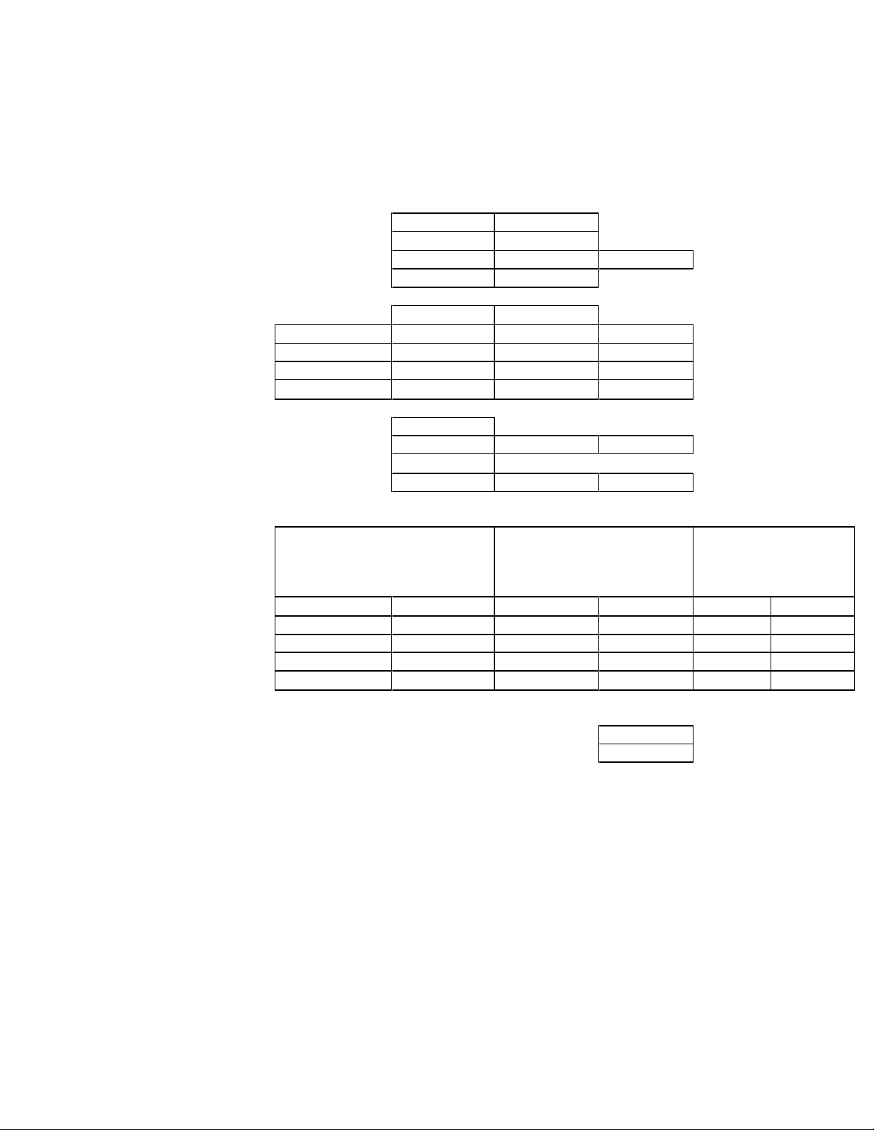
Model: SATA @ 6Gb/sec
4TB Model
Block size: 4k
Current
Current
Power
IO/Sec
+5V Amp
+12V Amp
Watts
Start up Peak DC [1]
0.28
1.54
Start up Peak AC
0.46
1.96
Idle_0, Avg
0.21
0.32
4.9
Idle Ripple
0.12
0.26
Random Peak [4]
0.52
1.78
Random RW 8kB Qd=1 Avg
40
0.23
0.41
6.1
Random RW 4kB Qd=1 Avg
139
0.23
0.51
7.3
Random RW 4kB Qd=4 Avg
206
0.24
0.74
10.1
Random R 4kB Qd=8 Avg [5]
233
0.24
0.73
9.9
Sequential Read Peak [4]
0.64
Sequential Read Avg [2]
0.52
0.34
6.7
Sequential Write Peak [4]
0.49
Sequential Write Avg [2]
0.42
0.38
6.7
Power Save Modes
Current
Power
Power
Saved
Recovery [1]
(PHY state: Active)
+5V Amp
+12V Amp
Watts
Watts[3]
12V DC
Peak
12V AC
Peak
Idle_A
0.21
0.32
4.9
0.0
Idle_B
0.12
0.27
3.9
1.1
Idle_C
0.12
0.20
3.0
1.9
1.00
1.17
Standby_Y
0.12
0.20
3.0
1.9
1.00
1.17
Sleep, Standby_Z
0.11
0.005
0.6
4.3
1.56
1.78
PHY power condition
Partial
0.2
Slumber
0.2
Notes
Sample size
10 HDD per model
Temperature
DE temperature = 40°C (25°C for Spin up)
Write Cache Enable
Off Bandwidth
All measurements are bandwidth limited to 20MHz
PHY
Single port, 6Gb/s
[1] 200ms windowed average
[2] Max transfer rate
[3] Power saved compared to Idle_0
[4] Maximum single peak in test samples
[5] Maximum power workload
6.3.2.2 SATA, 4TB, Block Size 4k, 6Gb/sec
Table 16 SATA Power Consumption, 4TB, 4k
Western Digital Hard Disk Drive OEM Specification
22
Page 37

Model: SATA @ 6Gb/sec
4TB Model
Block size: 512 native
Current
Current
Power
IO/Sec
+5V Amp
+12V Amp
Watts
Start up Peak DC [1]
0.35
1.56
Start up Peak AC
0.60
1.98
Idle_0, Avg
0.20
0.35
5.2
Idle Ripple
0.13
0.26
Random Peak [4]
0.78
1.88
Random RW 8kB Qd=1 Avg
40
0.23
0.45
6.6
Random RW 4kB Qd=1 Avg
83
0.22
0.56
7.8
Random RW 4kB Qd=4 Avg
114
0.22
0.64
8.8
Random R 4kB Qd=8 Avg [5]
144
0.22
0.70
9.5
Sequential Read Peak [4]
0.78
Sequential Read Avg [2]
0.51
0.36
6.9
Sequential Write Peak [4]
0.51
Sequential Write Avg [2]
0.42
0.40
6.9
Power Save Modes
Current
Power
Power
Saved
Recovery [1]
(PHY state: Active)
+5V Amp
+12V Amp
Watts
Watts[3]
12V DC
Peak
12V AC
Peak
Idle_A
0.20
0.35
5.2
0.0
Idle_B
0.11
0.30
4.2
1.0
Idle_C
0.11
0.22
3.2
2.0
1.00
1.17
Standby_Y
0.11
0.22
3.2
2.0
1.00
1.17
Sleep, Standby_Z
0.11
0.01
0.6
4.6
1.56
1.78
PHY power condition
Partial
0.2
Slumber
0.2
Notes
Sample size
10 HDD per model
Temperature
DE temperature = 40°C (25°C for Spin up)
Write Cache Enable
Off Bandwidth
All measurements are bandwidth limited to 20MHz
PHY
Single port, 6Gb/s
[1] 200ms windowed average
[2] Max transfer rate
[3] Power saved compared to Idle_0
[4] Maximum single peak in test samples
[5] Maximum power workload
6.3.2.3 SATA, 4TB, Block Size 512n, 6Gb/sec
Table 17 SATA Power Consumption, 4TB, 512n
Western Digital Hard Disk Drive OEM Specification
23
Page 38

6.3.3 Power Line Noise Limits
Noise Voltage (mV pp)
Frequency Range
+5V DC
250
100Hz-20MHz
+12V DC
800
100Hz-8KHz
450
8KHz-100KHz
250
100KHz-20MHz
Power Consumption
Efficiency at Idle_0
SATA W/GB
6TB
0.00102
4TB
0.00128
Table 18 Allowable Power Supply Noise Limits at Drive Power Connector
During drive operation, both 5 and 12-volt ripple are generated by the drive due to dynamic loading of the power
supply. This voltage ripple will add to existing power supply voltage ripple. The sum is the power line noise.
To prevent significant performance loss, the power line noise level when measured at the drive power connector
should be kept below the limits in the above table.
6.3.4 Power Consumption Efficiency
Table 19 Power Consumption Efficiency
24
Western Digital Hard Disk Drive OEM Specification
Page 39

6.4 Reliability
6.4.1 Data Integrity
When the write cache option is disabled, no customer data is lost during power loss. If the write cache option is
active or has been recently used, some data loss can occur during power loss. To prevent the loss of data at power
off, confirm the successful completion of a FLUSH CACHE (E7h) or FLUSH CACHE EXT (EAh) command.
6.4.2 Cable Noise Interference
To avoid any degradation of performance throughput or error rate when the interface cable is routed on top or comes
in contact with the HDA assembly, the drive must be grounded electrically to the system frame by four screws. The
common mode noise or voltage level difference between the system frame and power cable ground or AT interface
cable ground should be in the allowable level specified in the power requirement section.
6.4.3 Load/Unload
The product supports a minimum of 600,000 normal load/unloads in a 40° C environment.
Load/unload is invoked by transition of the HDD's power mode. (Chapter 4.5.3 Operating Modes)
Idle <-> Unload idle
Idle <-> Low rpm idle
6.4.4 Start/Stop Cycles
The drive withstands a minimum of 50,000 start/stop cycles in a 40° C environment and a minimum of 10,000
start/stop cycles in extreme temperature or humidity within the operating range.
6.4.5 Preventive Maintenance
None
6.4.6 Data Reliability
Probability of not recovering data is 1 in 1015 bits read.
LDPC on the fly/ offline data correction
4608 bit LDPC
This implementation recovers maximum 2500 bits single burst error by on the fly correction and maximum 3500
bits single burst error by offline correction
25
Western Digital Hard Disk Drive OEM Specification
Page 40

6.5 Mechanical Specifications
Height (mm)
Width (mm)
Length (mm)
Weight (grams)
26.1 Max
101.6 ± 0.25
147 Max
715 Max
6.5.1 Physical Dimensions
The following table shows the physical dimensions of the drive.
Table 20 Physical Dimensions
6.5.1.1 SATA
Figure 10 Top, bottom, side views and mechanical dimensions, with connector position (SATA)
All dimensions are in millimeters.
26
Western Digital Hard Disk Drive OEM Specification
Page 41

6.5.2 Drive Mounting
The drive will operate in all axes (6 directions).
Performance and error rate will stay within specification limits if the drive is operated in other orientations than that in
which it was formatted.
For reliable operation, the drive must be mounted in the system securely enough to prevent excessive motion or
vibration of the drive during seek operation or spindle rotation, using appropriate screws or equivalent mounting
hardware.
The recommended mounting screw torque is 0.6 - 1.0 Nm (6-10 Kgf.cm).
The recommended mounting screw depth is 3.8 mm maximum for bottom and 6.1 mm maximum for horizontal
mounting.
Drive level vibration test and shock test are to be conducted with the drive mounted to the table using the bottom four
screws.
6.5.3 Heads Unload and Actuator Lock
Heads are moved out from disks (unload) to protect the disk data during shipping, moving, or storage. Upon power
down, the heads are automatically unloaded from disk area and the locking mechanism of the head actuator will
secure the heads in unload position.
27
Western Digital Hard Disk Drive OEM Specification
Page 42

6.6 Vibration and Shock
Frequency
5 Hz
17 Hz
45 Hz
48 Hz
62 Hz
65 Hz
150 Hz
200 Hz
500 Hz
RMS
(m/sec2)
[(m/sec2)2/Hz]
1.9 x
10E–3
1.1 x
10E–1
1.1 x
10E–1
7.7 x
10E–1
7.7 x
10E–1
9.6 x
10E–2
9.6 x
10E–2
4.8 x
10E–2
4.8 x
10E-2
6.57
Frequency
20 Hz
100 Hz
200 Hz
800 Hz
1000 Hz
1500 Hz
1700 Hz
2000 Hz
RMS
(Rad/s2)
[(Rad/s2) 2/Hz]
1.90E
-02
1.90E
-02
1.87E
-01
1.87E
-01
5.33E
-02
7.70E
-03
4.00E
-03
4.00E
-03
12.5
All vibration and shock measurements recorded in this section are made with a drive that has no mounting
attachments for the systems. The input power for the measurements is applied to the normal drive mounting points.
6.6.1 Operating Vibration
6.6.1.1 Random Vibration (Linear)
The test is 30 minutes of random vibration using the power spectral density (PSD) levels shown below in each of
three mutually perpendicular axes. The disk drive will operate without non-recoverable errors when subjected to the
below random vibration levels.
Table 21 Random Vibration PSD Profile Break Points (operating)
The overall RMS (Root Mean Square) level is 6.57 m/sec2 (0.67 G).
6.6.1.2 Swept Sine Vibration (Linear)
The drive will meet the criteria shown below while operating in the specified conditions:
No errors occur with 4.9 m/sec2 (0.5 G) 0 to peak, 5 to 300 to 5 Hz sine wave, 0.5 oct/min sweep rate with
3-minute dwells at two major resonances
No data loss occurs with 9.8 m/sec2 (1 G) 0 to peak, 5 to 300 to 5 Hz sine wave, 0.5 oct/min sweep rate with
3-minute dwells at two major resonances
6.6.1.3 Random Vibration (Rotational)
The drive will meet the criteria shown below while operating in the specified conditions:
Less than 20% performance degradation
The overall RMS (Root Mean Square) level of vibration is 12.5Rad/sec^2. PSD profile is shown below.
Table 22 Random Vibration (Rotational) PSD Profile Break Points
28
Western Digital Hard Disk Drive OEM Specification
Page 43

6.6.2 Nonoperating Vibration
Frequency
2 Hz
4 Hz
8 Hz
40 Hz
55 Hz
70 Hz
200 Hz
[(m/sec2)2/Hz]
0.096
2.890
2.890
0.289
0.962
0.962
0.096
The drive does not sustain permanent damage or loss of previously recorded data after being subjected to the
environment described below
6.6.2.1 Random Vibration
The test consists of a random vibration applied for each of three mutually perpendicular axes with the time duration
of 10 minutes per axis. The PSD levels for the test simulate the shipping and relocation environment shown below.
The overall RMS (Root Mean Square) level of vibration is 10.2 m/sec2 (1.04 G).
Table 23 Random Vibration PSD Profile Break Points (nonoperating)
6.6.2.2
19.6 m/sec2 (2 G) (Zero to peak), 5 to 500 to 5 Hz sine wave
0.5 oct/min sweep rate
3 minutes dwell at two major resonances
Swept Sine Vibration
6.6.3 Operating Shock
The drive meets the following criteria while operating in the conditions described below. The shock test consists of
10 shock inputs in each axis and direction for total of 60. There must be a delay between shock pulses long enough
to allow the drive to complete all necessary error recovery procedures.
No error occurs with a 98.1 m/sec2 (10 G) half-sine shock pulse of 11 ms duration
No data loss occurs with a 294 m/sec2 (30 G) half-sine shock pulse of 4 ms duration
No data loss occurs with a 686 m/sec2 (70 G) half-sine shock pulse of 2 ms duration
6.6.4 Nonoperating Shock
The drive will operate without non-recoverable errors after being subjected to shock pulses with the following
characteristics.
6.6.4.1 Trapezoidal Shock Wave
Approximate square (trapezoidal) pulse shape
Approximate rise and fall time of pulse is 1 ms
Average acceleration level is 490 m/sec2 (50 G). (Average response curve value during the time following the 1
ms rise time and before the 1 ms fall with a time "duration of 11 ms")
Minimum velocity change is 4.23 m/sec
29
Western Digital Hard Disk Drive OEM Specification
Page 44

6.6.4.2 Sinusoidal Shock Wave
Acceleration Level (m/sec2) (G)
Duration (ms)
2940 (300G)
2
1470 (150G)
11
Duration
Rad/sec2
1 ms
30,000
2 ms
20,000
The shape is approximately half-sine pulse. The table below shows the maximum acceleration level and duration.
Table 24 Sinusoidal Shock Wave
6.6.5 Nonoperating Rotational Shock
All shock inputs shall be applied around the actuator pivot axis.
Table 25 Rotational Shock
30
Western Digital Hard Disk Drive OEM Specification
Page 45

6.7 Acoustics
Mode
7200rpm (Typical / Max)
Idle
2.9 / 3.4
Operating
3.6 / 4.0
The drive is powered on, disks spinning, track following, unit ready to receive and respond to
interface commands.
Continuous random cylinder selection and seek operation of the actuator with a dwell time at
each cylinder. The seek rate for the drive is to be calculated as shown below:
The upper limit criteria of the octave sound power levels are given in Bels relative to one picowatt and are shown in
the following table. The sound power emission levels are measured in accordance with ISO 7779.
Table 26 Sound Power Levels
Mode definition:
Dwell time = 0.5 x 60/RPM
Seek rate = 0.4 / (Average seek time + Dwell time)
6.8 Identification Labels
The following labels are affixed to every drive shipped from the drive manufacturing location in accordance with the
appropriate hard disk drive assembly drawing:
A label containing the WDC logo, the WDC part number, and the statement “Made by WDC, Ltd.” or WDC
approved equivalent
A label containing the drive model number, the manufacturing date code, the formatted capacity, the place of
manufacture, UL/CSA/CE/RCM mark logos, and WEEE/China RoHS logos
A bar code label containing the drive serial number
A label containing the jumper pin description
A user designed label per agreement
The above labels may be integrated with other labels.
31
Western Digital Hard Disk Drive OEM Specification
Page 46

6.9 Safety
6.9.1 UL and CSA Standard Conformity
The product is qualified per UL60950-1: Second Edition and CAN/CSA-C22.2 No.60950-1-07 Second Edition, for
use in Information Technology Equipment including Electric Business Equipment.
The UL recognition or the CSA certification is maintained for the product life.
The UL and C-UL recognition mark or the CSA monogram for CSA certification appear on the drive.
6.9.2 European Safety Mark
The product is approved by UL per Test requirement: EN 60950-1:2006+A11:2009+A1:2010+A12: 2011+A2:2013
allowing the use of the UL EU mark. The GS mark is not applicable to internal devices such as this product.
6.9.3 Flammability
The printed circuit boards used in this product are made of material with the UL recognized flammability rating of
V-1 or better. The flammability rating is marked or etched on the board. All other parts not considered electrical
components are made of material with the UL recognized flammability rating of V-2 minimum basically.
6.9.4 Safe Handling
The product is conditioned for safe handling in regards to sharp edges and corners.
6.9.5 Substance Restriction Requirements
The product complies with the Directive 2011/65/EU of the European Parliament on the restrictions of the use of the
certain hazardous substances in electrical and electronic equipment (RoHS) and with Halogen free requirements
based on the electronics industry standard, IEC 61249-2-21 (http://www.iec.ch/).
6.9.6 Secondary Circuit Protection
The product contains both 5V and 12V over-current protection circuitry.
32
Western Digital Hard Disk Drive OEM Specification
Page 47

6.10 Electromagnetic Compatibility
When installed in a suitable enclosure and exercised with a random accessing routine at maximum data rate, the
drive meets the following worldwide EMC requirements:
European Economic Community (EEC) directive number 76/889 related to the control of radio frequency
interference and the Verband Deutscher Elektrotechniker (VDE) requirements of Germany (GOP).Spectrum
Management Agency (SMA) EMC requirements of Australia. The SMA has approved RCM Marking for WDC
Japan.
United States Federal Communications Commission (FCC) Rules and Regulations (Class B), Part 15.
Operation is subject to the following two conditions:
1) This equipment may not cause harmful interference, and
2) this equipment must accept any interference received, including interference that may cause
undesired operation.
NOTE: this equipment has been tested and found to comply with the limits for a class B digital device, pursuant
to part 15 of the FCC rules. These limits are designed to provide reasonable protection against harmful
interference in residential installation. This equipment generates, uses and can radiate radio frequency energy
and if not installed and used in accordance with the instruction, may cause harmful interference to radio
communications. However, there is no guarantee that interference will not occur in a particular installation. If this
equipment does cause harmful interference to radio or television reception, which can be determined by turning
the equipment off and on, the user is encouraged to try to correct the interference by one or more of the
following measures:
– Reorient or relocate the receiving antenna.
– Increase the separation between the equipment and receiver.
– Connect the equipment into a different outlet from the receiver.
– Consult the dealer or an experienced radio/TV technician for help.
The user is cautioned that changes and modifications made to the equipment without the approval of
manufacturer could void the user's authority to operate this equipment.
(IF SHIELDED CABLES WERE USED DURING TESTING, ADD THE FOLLOWING PARAGRAPH.)
In order to maintain compliance with FCC regulations, shielded cables must be used with this equipment.
Operation with non- approved equipment or unshielded cables is likely to result in interference to radio and TV
reception.
6.10.1 CE Mark
The product is declared to be in conformity with requirements of the following EU directives under the sole
responsibility of WDC Japan, Ltd:
Council Directive 2014/30/EU on the approximation of laws of the Member States relating to electromagnetic
compatibility.
6.10.2 RCM Mark
The product complies with the following Australian EMC standard:
Limits and methods of measurement of radio disturbance characteristics of information technology, EN55032 : 2015
Class B.
6.10.3 BSMI Mark
The product complies with the Taiwan EMC standard “Limits and methods of measurement of radio disturbance
characteristics of information technology equipment, CNS 13438 Class B.”
33
Western Digital Hard Disk Drive OEM Specification
Page 48

6.10.4 KC Mark
The product complies with the Korea EMC standard. The regulation for certification of information and
communication equipment is based on “Telecommunications Basic Act” and “Radio Waves Act” Korea EMC
requirements are based technically on KN32/KN35 measurement standards and limits. KC standards are likewise
based on IEC standards.
6.11 Third Party Notices
This product includes the following third party software:
bzip2
http://www.bzip.org/index.html
LibTomCrypt
LibTomCrypt is licensed under DUAL licensing terms.
https://github.com/libtom/libtomcrypt/blob/develop/LICENSE
34
Western Digital Hard Disk Drive OEM Specification
Page 49

Part 2. Interface Specification
35
Western Digital Hard Disk Drive OEM Specification
Page 50

7 General
Device
Device indicates HUS726TxTALx6xx
Host
Host indicates the system that the device is attached to.
Check Power Mode
If the Extended Power Conditions feature set is disabled and the device is in Idle
mode, Check Power Mode command returns FFh by Sector Count Register,
instead of returning 80h. Refer to 11.1 “Check Power Mode” for detail.
COMRESET
COMRESET response is not the same as that of Power On Reset. Refer to
section 9.1 “Reset Response” for detail.
Download
Both Download Microcode and Download Microcode DMA are aborted when the
device is in security locked mode.
COMRESET response time
During 500ms from Power On Reset, COMINIT is not returned within 10ms as a
response to COMRESET.
Streaming Commands
When the device is in standby mode, Streaming Commands can’t be completed
while waiting for the spindle to reach operating speed even if execution time
exceeds specified CCTL (Command Completion Time Limit). The minimum
CCTL is 50ms.CCTL is set to 50ms when the specified value is shorter than
50ms.
SCT Error Recovery Control
When the device is in standby mode, any command where error recovery time
limit is specified can’t be completed while waiting for the spindle to reach
operating speed even if execution time exceeds specified recovery time limit. The
minimum time limit is 6.5 second. When the specified time limit is shorter than 6.5
second, the issued command is aborted.
7.1 Introduction
This specification describes the host interface of HUS726TxTALx6xx
The interface conforms to the following working documents of Information technology with certain limitations
described in the chapter 7.3 “Deviations from Standard” on page 36
- Serial ATA International Organization: Serial ATA Revision 3.2
Terminology
7.2
7.3 Deviations From Standard
The device conforms to the referenced specifications, with deviations described below.
Western Digital Hard Disk Drive OEM Specification
36
Page 51

8 Registers
Alternate Status Register
7 6 5 4 3 2 1
0
BSY
RDY
DF
DSC
/SERV
DRQ
COR
IDX
ERR
In Serial ATA, the host adapter contains a set of registers that shadow the contents of the traditional device registers,
referred to as the Shadow Register Block. Shadow Register Block registers are interface registers used for
delivering commands to the device or posting status from the device. About details, please refer to the Serial ATA
Specification.
In the following cases, the host adapter sets the BSY bit in its shadow Status Register and transmits a FIS to the
device containing the new contents.
Command register is written in the Shadow Register Block
Device Control register is written in the Shadow Register Block with a change of state of the SRST bit
COMRESET is requested
8.1 Alternate Status Register
Table 27 Alternate Status Register
This register contains the same information as the Status Register. The only difference is that reading this register
does not imply interrupt acknowledge or clear a pending interrupt. See 8.11 “Status Register” on the page 40 for the
definition of the bits in this register.
8.2 Command Register
This register contains the command code being sent to the device. Command execution begins immediately after
this register is written. The command set is shown in Table 95 Command Set on page 118.
All other registers required for the command must be set up before writing the Command Register.
8.3 Cylinder High Register
This register contains the high order bits of the starting cylinder address for any disk access. At the end of the
command, this register is updated to reflect the current cylinder number.
In LBA Mode this register contains Bits 16-23. At the end of the command, this register is updated to reflect the
current LBA Bits 16-23.
The cylinder number may be from zero to the number of cylinders minus one.
When 48-bit addressing commands are used, the “most recently written” content contains LBA Bits 16-23, and the
“previous content” contains Bits 40-47. The 48-bit Address feature set is described in 9.12.
37
Western Digital Hard Disk Drive OEM Specification
Page 52

8.4 Cylinder Low Register
Device Control Register
7 6 5 4 3 2 1
0
HOB - - - 1
SRST
-IEN
0
Bit Definitions
HOB
HOB (high order byte) is defined by the 48-bit Address feature set. A write to any Command
Register shall clear the HOB bit to zero.
SRST (RST)
Software Reset. The device is held reset when RST=1. Setting RST=0 re-enables the device.
The host must set RST=1 and wait for at least 5 microseconds before setting RST=0, to
ensure that the device recognizes the reset.
-IEN
Interrupt Enable. When –IEN=0, and the device is selected, device interrupts to the host will be
enabled. When –IEN=1, or the device is not selected, device interrupts to the host will be
disabled.
Device/Head Register
7 6 5 4 3 2 1
0
1 L 1
DRV
HS3
HS2
HS1
HS0
Bit Definitions
L
Binary encoded address mode select. When L=0, addressing is by CHS mode. When L=1,
addressing is by LBA mode.
DRV
Device. This product ignores this bit.
HS3,HS2,HS1,HS0
Head Select. These four bits indicate binary encoded address of the head. HS0 is the least
significant bit. At command completion, these bits are updated to reflect the currently
selected head.
The head number may be from zero to the number of heads minus one.
In LBA mode, HS3 through HS0 contain bits 24-27 of the LBA. At command completion,
these bits are updated to reflect the current LBA bits 24-27.
This register contains the low order bits of the starting cylinder address for any disk access. At the end of the
command, this register is updated to reflect the current cylinder number.
In LBA Mode this register contains Bits 8-15. At the end of the command, this register is updated to reflect the
current LBA Bits 8-15.
The cylinder number may be from zero to the number of cylinders minus one.
When 48-bit addressing commands are used, the “most recently written” content contains LBA Bits 8-15, and the
“previous content” contains Bits 32-39.
Device Control Register
8.5
Table 28 Device Control Register
8.6 Device/Head Register
Table 29 Device/Head Register
This register contains the device and head numbers.
Western Digital Hard Disk Drive OEM Specification
38
Page 53

8.7 Error Register
Error Register
7 6 5 4 3 2 1
0
ICRCE
UNC
0
IDNF
0
ABRT
TK0NF
AMNF
Bit Definitions
ICRCE (CRC)
Interface CRC Error. ICRCE=1 indicates a CRC error occurred during FIS transmission or FIS
reception.
UNC
Uncorrectable Data Error. UNC=1 indicates an uncorrectable data error has been encountered.
IDNF (IDN)
ID Not Found. IDN=1 indicates the requested sector’s ID field could not be found.
ABRT (ABT)
Aborted Command. ABT=1 indicates the requested command has been aborted due to a device
status error or an invalid parameter in an output register.
TK0NF (T0N)
Track 0 Not Found. T0N=1 indicates track 0 was not found during a Recalibrate command.
AMNF (AMN)
Address Mark Not Found. This product does not report this error. This bit is always zero.
Table 30 Error Register
This register contains status from the last command executed by the device, or a diagnostic code.
At the completion of any command except Execute Device Diagnostic, the contents of this register are valid always
even if ERR=0 in the Status Register.
Following a power on, a reset, or completion of an Execute Device Diagnostic command, this register contains a
diagnostic code. See 9.2 Diagnostic and Reset Considerations on page 42 for the definition.
8.8 Features Register
This register is command specific. This is used with the Set Features command, SMART Function Set command and
Format Unit command.
8.9 Sector Count Register
This register contains the number of sectors of data requested to be transferred on a read or write operation between
the host and the device. If the value in the register is set to 0, a count of 256 sectors (in 28-bit addressing) or 65,536
sectors (in 48-bit addressing) is specified.
If the register is zero at command completion, the command was successful. If not successfully completed, the
register contains the number of sectors which need to be transferred in order to complete the request.
The contents of the register are defined otherwise on some commands. These definitions are given in the command
descriptions.
8.10 Sector Number Register
This register contains the starting sector number for any disk data access for the subsequent command.
The sector number is from one to the maximum number of sectors per track.
In LBA mode, this register contains Bits 0-7. At the end of the command, this register is updated to reflect the current
LBA Bits 0-7.
When 48-bit commands are used, the “most recently written” content contains LBA Bits 0-7, and the “previous
content” contains Bits 24-31.
39
Western Digital Hard Disk Drive OEM Specification
Page 54

8.11 Status Register
Status Register
7 6 5 4 3 2 1
0
BSY
DRDY
DF
DSC
/SERV
DRQ
CORR
IDX
ERR
Bit Definitions
BSY
Busy. BSY=1 whenever the device is accessing the registers. The host should not read or write
any registers when BSY=1. If the host reads any register when BSY=1, the contents of the Status
Register will be returned.
DRDY (RDY)
Device Ready. RDY=1 indicates that the device is capable of responding to a command. RDY will
be set to 0 during power on until the device is ready to accept a command. If the device detects an
error while processing a command, RDY is set to 0 until the Status Register is read by the host, at
which time RDY is set back to 1.
DF
Device Fault. This product does not support DF bit. DF bit is always zero.
DSC
Device Seek Complete. DSC=1 indicates that a seek has completed and the device head is
settled over a track. DSC is set to 0 by the device just before a seek begins. When an error
occurs, this bit is not changed until the Status Register is read by the host, at which time the bit
again indicates the current seek complete status.
When the device enters into or is in Standby mode or Sleep mode, this bit is set by device in spite
of not spinning up.
SERV (SRV)
Service. This product does not support SERV bit.
DRQ
Data Request. DRQ=1 indicates that the device is ready to transfer a word or byte of data
between the host and the device. The host should not write the Command register when DRQ=1.
CORR (COR)
Corrected Data. Always 0.
IDX
Index. IDX=1 once per revolution. Since IDX=1 only for a very short time during each revolution,
the host may not see it set to 1 even if the host is reading the Status Register continuously.
Therefore, the host should not attempt to use IDX for timing purposes.
ERR
Error. ERR=1 indicates that an error occurred during execution of the previous command. The
Error Register should be read to determine the error type. The device sets ERR=0 when the next
command is received from the host.
Table 31 Status Register
This register contains the device status. The contents of this register are updated whenever an error occurs and at
the completion of each command.
If the host reads this register when an interrupt is pending, it is considered to be the interrupt acknowledge. Any
pending interrupt is cleared whenever this register is read.
If BSY=1, no other bits in the register are valid.
Western Digital Hard Disk Drive OEM Specification
40
Page 55

9 General Operation Descriptions
Power On Reset (POR)
The device executes a series of electrical circuitry diagnostics.
COMRESET
COMRESET is issued in Serial ATA bus.
The device resets the interface circuitry as well as Soft Reset.
Soft Reset (Software Reset)
SRST bit in the Device Control Register is set, and then is reset.
The device resets the interface circuitry according to the Set Features requirement.
POR
COMRESET
Soft Reset
Aborting Host interface
- o o
Aborting Device operation
-
(*1)
(*1)
Initialization of hardware
o x x
Internal diagnostic
o x x
Spinning spindle
(*6) x x
Initialization of registers (*2)
o o o
Reverting programmed parameters to default
o
(*3)
(*3)
- Number of CHS
(set by Initialize Device Parameter)
- Multiple mode
- Write cache
- Read look-ahead
- ECC bytes
Disable Standby timer
o x x
Power mode
(*5)
(*4)
(*4)
9.1 Reset Response
There are three types of reset in ATA as follows:
The actions of each reset are shown in Table 32.
Table 32 Reset Response
Table Notes
(*1) Execute after the data in write cache has been written.
(*2) Default value on POR is shown in Table 34 Default Register Values on page 42.
(*3) The Set Features command with Feature register = CCh enables the device to revert these parameters to
the power on defaults.
(*4) In the case of Sleep mode, the device goes to Standby mode. In other case, the device does not change
current mode.
(*5) Idle when Power-Up in Standby feature set is disabled. Standby when Power-Up in Standby feature set is
enabled.
(*6) Spinning up when Power-Up in Standby feature set is disabled. Standby when Power-Up in Standby feature
set is enabled.
41
Western Digital Hard Disk Drive OEM Specification
o ---- Execute
x ---- Not execute
Page 56

9.1.1 Register Initialization
Register
Default Value
Error
Diagnostic Code
Sector Count
01h
Sector Number
01h
Cylinder Low
00h
Cylinder High
00h
Device/Head
00h
Status
50h
Alternate Status
50h
Code
Description
01h
No error Detected
02h
Formatter device error
03h
Sector buffer error
04h
ECC circuitry error
05h
Controller microprocessor error
Table 33 Default Register Values
After power on, hard reset, or software reset, the register values are initialized as shown in Table 33.
Table 34 Diagnostic Codes
The meaning of the Error Register diagnostic codes resulting from power on, hard reset or the Execute Device
Diagnostic command is shown in Table 34.
9.2 Diagnostic and Reset Considerations
In each case of Power on Reset, COMRESET, Soft reset, and EXECUTE DEVICE DIAGNOSTIC command, the
device is diagnosed. An Error register is set as shown in Table 34.
42
Western Digital Hard Disk Drive OEM Specification
Page 57

9.3 Sector Addressing Mode
Device/Head
LBA
bits
27-24
Cylinder High
LBA
bits
23-16
Cylinder Low
LBA
bits
15- 8
Sector Number
LBA
bits
7- 0
All addressing of data sectors recorded on the device’s media is by a logical sector address. The logical CHS
address for HUS726TxTALx6xx is different from the actual physical CHS location of the data sector on the disk
media. All addressing of data sectors recorded on the device’s media.
HUS726TxTALx6xx support both Logical CHS Addressing Mode and LBA Addressing Mode as the sector
addressing mode.
The host system may select either the currently selected CHS translation addressing or LBA addressing on a
command-by-command basis by using the L bit in the DEVICE/HEAD register. So a host system must set the L bit to
1 if the host uses LBA Addressing mode.
9.3.1 Logical CHS Addressing Mode
The logical CHS addressing is made up of three fields: the cylinder number, the head number and the sector number.
Sectors are numbered from 1 to the maximum value allowed by the current CHS translation mode but cannot exceed
255(0FFh). Heads are numbered from 0 to the maximum value allowed by the current CHS translation mode but
cannot exceed 15(0Fh). Cylinders are numbered from 0 to the maximum value allowed by the current CHS
translation mode but cannot exceed 65535(0FFFFh).
When the host selects a CHS translation mode using the INITIALIZE DEVICE PARAMETERS command, the host
requests the number of sectors per logical track and the number of heads per logical cylinder. The device then
computes the number of logical cylinders available in requested mode.
The default CHS translation mode is described in the Identify Device Information. The current CHS translation mode
also is described in the Identify Device Information.
9.3.2 LBA Addressing Mode
Logical sectors on the device shall be linearly mapped with the first LBA addressed sector (sector 0) being the same
sector as the first logical CHS addressed sector (cylinder 0, head 0, sector 1). Irrespective of the logical CHS
translation mode currently in effect, the LBA address of a given logical sector does not change. The following is
always true:
LBA = ((cylinder * heads_per_cylinder + heads)
* sectors_per_track ) + sector - 1
Where heads_per_cylinder and sectors_per_track are the current translation mode values.
On LBA addressing mode, the LBA value is set to the following register.
43
Western Digital Hard Disk Drive OEM Specification
Page 58

9.4 Power Management Feature
The power management feature set allows an application client to modify the behavior of a device in a manner that
reduces the power required to operate. The power management feature set provides a set of commands and a timer
that enables a device to implement low power consumption modes.
The Power Management feature set implements the following set of functions.
1. A Standby timer
2. Idle command
3. Idle Immediate command
4. Sleep command
5. Standby command
6. Standby Immediate command
9.4.1 Power Mode
The lowest power consumption when the device is powered on occurs in Sleep Mode. When in sleep mode, the
device requires a reset to be activated.
In Idle Mode the device is capable of responding immediately to media access requests.
In Active Mode the device is under executing a command or accessing the disk media with read look-ahead function
or writes cache function.
9.4.1.1 Active Idle Mode
The electronics repeats on and off. And heads are track following and seeking, however the spindle is still rotated at
the full speed.
9.4.1.2 Low Power Idle Mode
Additional electronics are powered off, and heads are unloaded on the ramp, however the spindle is still rotated at
the full speed.
9.4.1.3 Low RPM Idle Mode
The heads are unloaded on the ramp, and the spindle is rotated at the 85-90% of the full speed.
9.4.1.4 Standby Mode
The device interface is capable of accepting commands, but as the media may not immediately accessible, there is a
delay while waiting for the spindle to reach operating speed.
44
Western Digital Hard Disk Drive OEM Specification
Page 59

9.4.2 Power Management Commands
Mode
BSY
RDY
Interface active
Media
Active x x Yes
Active
Idle 0 1 Yes
Active
Standby
0 1
Yes
Inactive
sleep x x No
Inactive
The Check Power Mode command allows a host to determine if a device is in, going, to or leaving standby or idle
mode.
The Idle and Idle Immediate commands move a device to idle mode immediately from the active or standby modes.
The idle command also sets the standby timer count and enables or disables the standby timer.
The Standby and Standby Immediate commands move a device to standby mode immediately from the active or idle
modes. The standby command also sets the standby timer count and enables or disables the Standby timer.
The Sleep command moves a device to sleep mode. The device’s interface becomes inactive after the device
reports command completion for the sleep command. A device only transitions from sleep mode after processing
hardware reset, a software reset.
9.4.3 Standby Timer
The standby timer provides a method for the device to automatically enter standby mode from either active or idle
mode following a host programmed period of inactivity. If the device is in the active or idle mode, the device waits for
the specified time period and if no command is received, the device automatically enters the standby mode.
If the value of SECTOR COUNT Register on Idle command or Standby command is set to 00h, the standby timer is
disabled.
9.4.4 Interface Capability for Power Modes
Each power mode affects the physical interface as defined in the following table:
Table 35 Power conditions
Ready (RDY) is not a power condition. A device may post ready at the interface even though the media may not be
accessible.
45
Western Digital Hard Disk Drive OEM Specification
Page 60

9.5 SMART Function
The intent of Self-monitoring, analysis and reporting technology (SMART) is to protect user data and prevent
unscheduled system downtime that may be caused by predictable degradation and/or fault of the device. By
monitoring and storing critical performance and calibration parameters, SMART devices employ sophisticated data
analysis algorithms to predict the likelihood of near-term degradation or fault condition. By alerting the host system of
a negative reliability status condition, the host system can warn the user of the impending risk of a data loss and
advise the user of appropriate action.
9.5.1 Attributes
Attributes are the specific performance or calibration parameters that are used in analyzing the status of the device.
Attributes are selected by the device manufacturer based on that attribute’s ability to contribute to the prediction of
degrading or faulty conditions for that particular device. The specific set of attributes being used and the identity of
these attributes is vendor specific and proprietary.
9.5.2 Attribute Values
Attribute values are used to represent the relative reliability of individual performance or calibration attributes. The
valid range of attribute values is from 1 to 253 decimal. Higher attribute values indicate that the analysis algorithms
being used by the device are predicting a lower probability of a degrading or faulty condition existing. Accordingly,
lower attribute values indicate that the analysis algorithms being used by the device are predicting a higher
probability of a degrading or faulty condition existing.
9.5.3 Attribute Thresholds
Each attribute value has a corresponding attribute threshold limit which is used for direct comparison to the attribute
value to indicate the existence of a degrading or faulty condition. The numerical values of the attribute thresholds are
determined by the device manufacturer through design and reliability testing and analysis. Each attribute threshold
represents the lowest limit to which its corresponding attribute value can be equal while still retaining a positive
reliability status. Attribute thresholds are set at the device manufacturer’s factory and cannot be changed in the field.
The valid range for attribute thresholds is from 1 through 253 decimal.
9.5.4 Threshold Exceeded Condition
If one or more attribute values, whose Pre-failure bit of their status flag is set, are less than or equal to their
corresponding attribute thresholds, then the device reliability status is negative, indicating an impending degrading or
faulty condition.
9.5.5 SMART Commands
The SMART commands provide access to attribute values, attribute thresholds and other logging and reporting
information.
9.5.6 Off-Line Read Scanning
The device provides the off-line read scanning feature with reallocation. This is the extension of the off-line data
collection capability. The device performs the entire read scan with reallocation for the marginal sectors to prevent
the user data lost.
If interrupted by the host during the read scanning, the device services the host command.
Western Digital Hard Disk Drive OEM Specification
46
Page 61

9.5.7 Error Log
Logging of reported errors is supported. The device provides information on the last five errors that the device
reported as described in SMART error log sector. The device may also provide additional vendor specific information
on these reported errors. The error log is not disabled when SMART is disabled. Disabling SMART shall disable the
delivering of error log information via the SMART READ LOG SECTOR command.
If a device receives a firmware modification, all error log data is discarded and the device error count for the life of
the device is reset to zero.
9.5.8 Self-Test
The device provides the self-test features which are initiated by SMART Execute Off-line Immediate command. The
self-test checks the fault of the device, reports the test status in Device Attributes Data and stores the test result in
the SMART self-test log sector as described in SMART self-test log data structure. All SMART attributes are updated
accordingly during the execution of self-test.
If interrupted by the host during the self-tests, the device services the host command.
If the device receives a firmware modification, all self-test log data is discarded.
47
Western Digital Hard Disk Drive OEM Specification
Page 62

9.6 Security Mode Feature Set
Security Set Password
(‘F1’h)
Security Unlock
(‘F2’h)
Security Erase Prepare
(‘F3’h)
Security Erase Unit
(‘F4’h)
Security Freeze Lock
(‘F5’h)
Security Disable Password
(‘F6’h)
Device Locked mode
The device disables media access commands after power on. Media accesses
commands are enabled by either a security unlock command or a security erases unit
command.
Device Unlocked mode
The device enables all commands. If a password is not set this mode is entered after
power on, otherwise it is entered by a security unlock or a security erases unit command.
Device Frozen mode
The device enables all commands except those which can update the device lock
function, set/change password. The device enters this mode via a Security Freeze Lock
command. It cannot quit this mode until power off.
High level security
When the device lock function is enabled and the User Password is forgotten the device
can be unlocked via a Master Password.
Maximum level security
When the device lock function is enabled and the User Password is forgotten then only
the Master Password with a Security Erase Unit command can unlock the device. Then
user data is erased.
Master Password
When the Master Password is set, the device does NOT enable the Device Lock Function, and
the device can NOT be locked with the Master Password, but the Master Password can be
used for unlocking the device locked.
Identify Device Information word 92 contains the value of the Master Password Revision Code
set when the Master Password was last changed. Valid values are 0001h through FFFEh.
User Password
The User Password should be given or changed by a system user. When the User Password is
set, the device enables the Device Lock Function, and then the device is locked on next power
on reset or hard reset.
Security Mode Feature Set is a powerful security feature. With a device lock password, a user can prevent
unauthorized access to hard disk device even if the device is removed from the computer.
The following commands are supported for this feature.
Execution of these commands is restricted for the Trusted Computing Group feature set. That is, these commands
operate only in the state that is the Manufactured-Inactivate state by the Trusted Computing Group feature set.
Moreover, these commands are aborted in the state that is activated to the Manufactured state by the Trusted
Computing Group feature set.
9.6.1 Security Mode
Following security modes are provided.
9.6.2 Security Level
Following security levels are provided.
9.6.3 Password
This function can have 2 types of passwords as described below.
The system manufacturer/dealer who intends to enable the device lock function for the end users, must set the
master password even if only single level password protection is required.
48
Western Digital Hard Disk Drive OEM Specification
Page 63

9.6.4 Operation Example
(ref.)
< Setting Password > < No Setting Password >
POR POR
Set Password with User Password
Normal Operation Normal Operation
Power off Power off
POR Device locked mode POR Device locked mode
9.6.4.1 Master Password Setting
The system manufacturer/dealer can set a new Master Password from default Master Password using the 2 Set
Password command, without enabling the Device Lock Function.
The Master Password Revision Code is set to FFFEh as shipping default by the HDD manufacturer
9.6.4.2 User Password Setting
When a User Password is set, the device will automatically enter lock mode the next time the device is powered on.
Figure 11 Initial Setting
Western Digital Hard Disk Drive OEM Specification
49
Page 64

9.6.4.3 Operation from POR after User Password is Set
POR
Device Locked mode
Unlock CMD Erase Prepare Media access
command (*1)
Non-Media access
command (*1)
Password
Match ?
Complete
Erase Unit
Lock function
Disable
Enter Device
Unlock mode
Erase Unit
Password
Match ?
Normal operation : All commands are available
Freeze Lock command
Enter Device Frozen mode
Normal Operation except Set Password,
Disable Password, Erase Unit, Unlock commands.
Reject
Complete
N
Y
N
Y
When Device Lock Function is enabled, the device rejects media access command until a Security Unlock command
is successfully completed.
(*1) Refer to 9.6.5 on the page.52
Figure 12 Usual Operation
Western Digital Hard Disk Drive OEM Specification
50
Page 65

9.6.4.4 User Password Lost
LEVEL ?
Normal operation but data lost
Maxinum
High
User Password Loat
Erase Unit Command
with Maseter Password
Erase Prepare Command
Unlock CMD with Master Password
Normal operation
If the User Password is forgotten and High level security is set, the system user can’t access any data. However, the
device can be unlocked using the Master Password.
If a system user forgets the User Password and Maximum security level is set, data access is impossible. However,
the device can be unlocked using the Security Erase Unit command to unlock the device and erase all user data with
the Master Password.
Figure 13 Password Lost
9.6.4.5 Attempt Limit for SECURITY UNLOCK Command
The SECURITY UNLOCK command has an attempt limit. The purpose of this attempt limit is to prevent that
someone attempts to unlock the drive by using various passwords many times.
The device counts the password mismatch. If the password does not match, the device counts it up without
distinguishing the Master password and the User password. If the count reaches 5, EXPIRE bit (bit 4) of Word 128 in
Identify Device information is set, and then SECURITY ERASE UNIT command and SECURITY UNLOCK command
are aborted until a hard reset or a power off. The count and EXPIRE bit are cleared after a power on reset or a hard
reset.
51
Western Digital Hard Disk Drive OEM Specification
Page 66

9.6.5 Command Table
Command
Locked Mode
Unlocked Mode
Frozen Mode
Check Power Mode
Executable
Executable
Executable
Configure Stream
Command aborted
Executable
Executable
Crypto Scramble Ext
Command aborted
Executable
Executable
Device Configuration Restore
Command aborted
Executable
Executable
Device Configuration Freeze Lock
Command aborted
Executable
Executable
Device Configuration Identify
Command aborted
Executable
Executable
Device Configuration Set
Command aborted
Executable
Executable
Download Microcode
Command aborted
Executable
Executable
Download Microcode DMA
Command aborted
Executable
Executable
Execute Device Diagnostic
Executable
Executable
Executable
Flush Cache
Command aborted
Executable
Executable
Flush Cache Ext
Command aborted
Executable
Executable
Format Track
Command aborted
Executable
Executable
Identify Device
Executable
Executable
Executable
Idle
Executable
Executable
Executable
Idle Immediate
Executable
Executable
Executable
Initialize Device Parameters
Executable
Executable
Executable
NCQ NON-DATA
Command aborted
Executable
Executable
Overwrite Ext
Command aborted
Executable
Executable
Read Buffer
Executable
Executable
Executable
Read DMA
Command aborted
Executable
Executable
Read DMA Ext
Command aborted
Executable
Executable
Read FPDMA Queued
Command aborted
Executable
Executable
Read Log Ext
Executable
Executable
Executable
Read Log DMA Ext
Executable
Executable
Executable
Read Multiple
Command aborted
Executable
Executable
Read Multiple Ext
Command aborted
Executable
Executable
Read Native Max Address
Executable
Executable
Executable
Read Native Max Ext
Executable
Executable
Executable
Read Sector(s)
Command aborted
Executable
Executable
Read Sector(s) Ext
Command aborted
Executable
Executable
Read Stream DMA Ext
Command aborted
Executable
Executable
Read Stream Ext
Command aborted
Executable
Executable
Read Verify Sector(s)
Command aborted
Executable
Executable
Read Verify Sector(s) Ext
Command aborted
Executable
Executable
Recalibrate
Executable
Executable
Executable
Request Sense Data Ext
Executable
Executable
Executable
Sanitize Freeze Lock Ext
Command aborted
Executable
Executable
Sanitize Status Ext
Executable
Executable
Executable
This table shows the device’s response to commands when the Security Mode Feature Set (Device lock function) is
enabled.
Table 36 Command table for device lock operation -1
52
Western Digital Hard Disk Drive OEM Specification
Page 67

Command
Locked Mode
Unlocked Mode
Frozen Mode
SCT Read/Write Long
Command aborted
Command aborted
Command aborted
SCT Write Same
Command aborted
Executable
Executable
SCT Error Recovery Control
Command aborted
Executable
Executable
SCT Feature Control
Command aborted
Executable
Executable
SCT Data Table
Command aborted
Executable
Executable
SCT Read Status
Executable
Executable
Executable
Security Disable Password
Command aborted
Executable
Command aborted
Security Erase Prepare
Executable
Executable
Command aborted
Security Erase Unit
Executable
Executable
Command aborted
Security Freeze Lock
Command aborted
Executable
Executable
Security Set Password
Command aborted
Executable
Command aborted
Security Unlock
Executable
Executable
Command aborted
Seek
Executable
Executable
Executable
Set Features
Executable
Executable
Executable
Set Max Address
Command aborted
Executable
Executable
Set Max Address Ext
Command aborted
Executable
Executable
Set Multiple Mode
Executable
Executable
Executable
Sleep
Executable
Executable
Executable
SMART Disable Operations
Executable
Executable
Executable
SMART Enable/Disable Attribute Autosave
Executable
Executable
Executable
SMART Enable Operations
Executable
Executable
Executable
SMART Execute Off-line Immediate
Executable
Executable
Executable
SMART Read Attribute Values
Executable
Executable
Executable
SMART Read Attribute Thresholds
Executable
Executable
Executable
SMART Return Status
Executable
Executable
Executable
SMART Save Attribute Values
Executable
Executable
Executable
SMART Read Log Sector
Executable
Executable
Executable
SMART Write Log Sector
Executable
Executable
Executable
SMART Enable/Disable Automatic Off-Line
Executable
Executable
Executable
Standby
Executable
Executable
Executable
Standby Immediate
Executable
Executable
Executable
Trusted Receive
Command aborted
Executable
Executable
Trusted Receive DMA
Command aborted
Executable
Executable
Trusted Send
Command aborted
Executable
Executable
Trusted Send DMA
Command aborted
Executable
Executable
Write Buffer
Executable
Executable
Executable
Write DMA
Command aborted
Executable
Executable
Write DMA Ext
Command aborted
Executable
Executable
Table 37 Command table for device lock operation -2
Western Digital Hard Disk Drive OEM Specification
53
Page 68

Command
Locked Mode
Unlocked Mode
Frozen Mode
Write DMA FUA Ext
Command aborted
Executable
Executable
Write FPDMA Queued
Command aborted
Executable
Executable
Write Log Ext
Command aborted
Executable
Executable
Write Log DMA Ext
Command aborted
Executable
Executable
Write Multiple
Command aborted
Executable
Executable
Write Multiple Ext
Command aborted
Executable
Executable
Write Multiple FUA Ext
Command aborted
Executable
Executable
Write Sector(s)
Command aborted
Executable
Executable
Write Sector(s) Ext
Command aborted
Executable
Executable
Write Stream DMA Ext
Command aborted
Executable
Executable
Write Stream Ext
Command aborted
Executable
Executable
Write Uncorrectable Ext
Command aborted
Executable
Executable
Table 38 Command table for device lock operation -3
54
Western Digital Hard Disk Drive OEM Specification
Page 69

9.7 Host Protected Area Feature
Read Native Max ADDRESS
(‘F8’h)
Set Max ADDRESS
(‘F9’h)
Capacity (native)
:
6,498,680,832
byte (6.4GB)
Max LBA (native)
:
12,692,735
(0FFFFFh)
Required size for protected area
:
206,438,400
byte
Required blocks for protected area
:
403,200
(062700h)
Customer usable device size
:
6,292,242,432
byte (6.2GB)
Customer usable sector count
:
12,289,536
(BB8600h)
LBA range for protected area
:
BB8600h to C1ACFFh
Host Protected Area Feature is to provide the ‘protected area’ which cannot be accessed via conventional method.
This ‘protected area’ is used to contain critical system data such as BIOS or system management information. The
contents of entire system main memory may also be dumped into ‘protected area’ to resume after system power off.
The LBA/CYL changed by following command affects the Identify Device Information.
The following set of commands is implemented for this function.
9.7.1 Example for Operation (in LBA mode)
Assumptions:
For better understanding, the following example uses actual values for LBA, size, etc. Since it is just an example,
these values could be different.
Device characteristics
1. Shipping HDDs from HDD manufacturer
When the HDDs are shipped from HDD manufacturer, the device has been tested to have usable capacity of
6.4GB besides flagged media defects not to be visible by system.
2. Preparing HDDs at system manufacturer
Special utility software is required to define the size of protected area and store the data into it.
The sequence is:
Issue Read Native Max Address command to get the real device maximum LBA. Returned value shows that
native device Maximum LBA is 12,692,735 (C1ACFFh) regardless of the current setting.
Make entire device be accessible including the protected area by setting device Maximum LBA as
12,692,735 (C1ACFFh) via Set Max Address command. The option could be either nonvolatile or volatile.
Test the sectors for protected area (LBA >= 12,289,536 (BB8600h)) if required.
Write information data such as BIOS code within the protected area.
Change maximum LBA using Set Max Address command to 12,289,535 (BB85FFh) with nonvolatile option.
From this point, the protected area cannot be accessed till next Set Max Address command is issued. Any
BIOSes, device drivers, or application software access the HDD as if that is the 6.2GB device because the
device acts exactly the same as real 6.2GB device does.
3. Conventional usage without system software support
Since the HDD works as 6.2GB device, there is no special care to use this device for normal use.
55
Western Digital Hard Disk Drive OEM Specification
Page 70

4. Advanced usage using protected area
The data in the protected area is accessed by following.
Issue Read Native Max Address command to get the real device maximum LBA. Returned value shows that
native device Maximum LBA is 12,692,735 (C1ACFFh) regardless of the current setting.
Make entire device be accessible including the protected area by setting device Maximum LBA as
12,692,735 (C1ACFFh) via Set Max Address command with volatile option. By using this option, unexpected
power removal or reset will not make the protected area remained accessible.
Read information data from protected area.
Issue hard reset or POR to inhibit any access to the protected area.
9.7.2 Security Extensions
1. Set Max Set Password
2. Set Max Lock
3. Set Max Freeze Lock
4. Set Max Unlock.
The Set Max Set Password command allows the host to define the password to be used during the current power on
cycle. The password does not persist over a power cycle but does persist over a hardware or software reset. This
password is not related to the password used for the Security Mode Feature set. When the password is set the
device is in the Set_Max_Unlocked mode. The Set Max Lock command allows the host to disable the Set Max
commands (except set Max Unlock) until the next power cycle or the issuance and acceptance of the Set Max
Unlock command. When this command is accepted the device is in the Set_Max_Locked mode. The Set Max Unlock
command changes the device from the Set_Max_Locked mode to the Set_Max_Unlocked mode. The Set Max
Freeze Lock command allows the host to disable the Set Max commands (including Set Max UNLOCK) until the next
power cycle. When this command is accepted the device is in the Set_Max_Frozen mode.
The IDENTIFY DEVICE response word 83, bit 8 indicates that this extension is supported if set, and word 86, bit 8
indicate the Set Max security extension enabled if set.
56
Western Digital Hard Disk Drive OEM Specification
Page 71

9.8 Write Cache Function
Write cache is a performance enhancement whereby the device reports as completing the write command (Write
Sector(s), Write Multiple and Write DMA) to the host as soon as the device has received all of the data into its buffer.
And the device assumes responsibility to write the data subsequently onto the disk.
While writing data after completed acknowledgment of a write command, soft reset or hard reset does not affect
its operation. But power off terminates writing operation immediately and unwritten data are to be lost.
Soft reset, Standby (Immediate) command and Flush Cache commands during writing the cached data are
executed after the completion of writing to media. So the host system can confirm the completion of write cache
operation by issuing Soft reset, Standby (Immediate) command or Flush Cache command to the device before
power off.
9.9 Reassign Function
The reassign Function is used with read commands and write commands. The sectors of data for reassignment are
prepared as the spare data sector.
This reassignment information is registered internally, and the information is available right after completing the
reassign function. Also the information is used on the next power on reset or hard reset.
If the number of the spare sector reaches 0 sectors, the reassign function will be disabled automatically.
The spare tracks for reassignment are located at regular intervals from Cylinder 0. As a result of reassignment, the
physical location of logically sequenced sectors will be dispersed.
9.9.1 Auto Reassign Function
The sectors those show some errors may be reallocated automatically when specific conditions are met. The spare
tracks for reallocation are located at regular intervals from Cylinder 0. The conditions for auto-reallocation are
described below.
None recovered write errors
When a write operation cannot be completed after the Error Recovery Procedure (ERP) is fully carried out, the
sector(s) are reallocated to the spare location. An error is reported to the host system only when the write cache is
disabled and the auto reallocation is failed.
If the write cache function is ENABLED, and when the number of available spare sectors reaches 0 sectors, both
auto reassign function and write cache function are disabled automatically.
None recovered read errors
When a read operation is failed after defined ERP is fully carried out, a hard error is reported to the host system. This
location is registered internally as a candidate for the reallocation. When a registered location is specified as a target
of a write operation, a sequence of media verification is performed automatically. When the result of this verification
meets the criteria, this sector is reallocated.
Recovered read errors
When a read operation for a sector failed once then recovered at the specific ERP step, this sector of data is
reallocated automatically. A media verification sequence may be run prior to the relocation according to the
pre-defined conditions.
57
Western Digital Hard Disk Drive OEM Specification
Page 72

9.10 Power-Up in Standby Feature Set
Power-Up In Standby feature set allows devices to be powered-up into the Standby power management state to
minimize inrush current at power-up and to allow the host to sequence the spin-up of devices.
This feature set will be enabled/disabled via the SET FEATURES command. The enabling of this feature set shall be
persistent after power cycle.
A device needs a SET FEATURES subcommand to spin-up to active state when the device has powered-up into
Standby. The device remains in Standby until the SET FEATURES subcommand is received.
If power-up into Standby is enabled, when an IDENTIFY DEVICE is received while the device is in Standby as a
result of powering up into Standby, the device shall set word 0 bit 2 to one to indicate that the response is incomplete,
then only words 0 and 2 are correctly reported.
The IDENTIFY DEVICE information indicates the states as follows:
identify device information is complete or incomplete
this feature set is implemented
this feature set is enabled or disabled
the device needs the Set Features command to spin-up into active state
9.11 Advanced Power Management Feature Set (APM)
This feature allows the host to select an advanced power management level. The advanced power management
level is a scale from the lowest power consumption setting of 01h to the maximum performance level of FEh. Device
performance may increase with increasing advanced power management levels. Device power consumption may
increase with increasing advanced power management levels. The advanced power management levels contain
discrete bands, described in the section of Set Feature command in detail. This feature set uses the following
functions:
1. A SET FEATURES subcommand to enable Advanced Power Management
2. A SET FEATURES subcommand to disable Advanced Power Management
Advanced Power Management is independent of the Standby timer setting. If both Advanced Power Management
and the Standby timer are set, the device will go to the Standby state when the timer times out or the device’s
Advanced Power Management algorithm indicates that the Standby state should be entered.
The IDENTIFY DEVICE response word 83, bit 3 indicates that Advanced Power Management feature is supported if
set. Word 86, bit 3 indicates that Advanced Power Management is enabled if set. Word 91, bits 7-0 contain the
current Advanced Power Management level if Advanced Power Management is enabled.
9.12 48-bit Address Feature Set
The 48-bit Address feature set allows devices:
a) with capacities up to 281,474,976,710,655 logical sectors (i.e., up to 144,115,188,075,855,360 bytes for a
512-byte logical block device); and
b) to transfer up to 65 536 logical sectors in a single command.
The 48-bit Address feature set operates in LBA addressing only. Devices also implement commands using 28-bit
addressing, and 28-bit and 48-bit commands may be intermixed.
Support of the 48-bit Address feature set is indicated in the Identify Device response bit 10 words 83. In addition, the
maximum user LBA address accessible by 48-bit addressable commands is contained in Identify Device response
words 230 through 233.
When the 48-bit Address feature set is implemented, the native maximum address is the value returned by a Read
Native Max Address Ext command. If the native maximum address is equal to or less than 268,435,455, a Read
Native Max Address shall return the native maximum address. If the native maximum address is greater than
268,435,455, a Read Native Max Address shall return a value of 268,435,455.
58
Western Digital Hard Disk Drive OEM Specification
Page 73

9.13 Streaming Feature Set
The Streaming feature set is an optional feature set that allows a host to request delivery of data from a contiguous
logical block address range within an allotted time. This places a priority on time to access the data rather than the
integrity of the data. Streaming feature set commands only support 48-bit addressing.
A device that implements the Streaming feature set shall implement the following minimum set of commands:
Configure Stream
Read Stream Ext
Write Stream Ext
Read Stream DMA Ext
Write Stream DMA Ext
Read Log Ext
Support of the Streaming feature set is indicated in Identify Device work 84 bit 4.
Note that PIO versions of these commands limit the transfer rate (16.6 MB/s), provide no CRC protection, and limit status
reporting as compared to a DMA implementation.
9.13.1 Streaming Commands
The streaming commands are defined to be time critical data transfers rather than the standard data integrity critical
commands. Each command shall be completed within the time specified in the Configure Stream command or in the
streaming command itself in order to ensure the stream requirements of the AV type application. The device may
execute background tasks as long as the Read Stream and Write Stream command execution time limits are still
met.
Using the Configure Stream command, the host may define the various stream properties including the default
Command Completion Time Limit (CCTL) to assist the device in setting up its caching for best performance. If the
host does not use a Configure Stream command, the device shall use the CCTL specified in each streaming
command, and the time limit is effective for one time only. If the CCTL is not set by Configure Stream command, the
operation of a streaming command with a zero CCTL is device vendor specific. If Stream ID is not set by a Configure
Stream command, the device shall operate according to the Stream ID set by the streaming command. The
operation is device vendor specific.
The streaming commands may access any user LBA on a device. These commands may be interspersed with
non-streaming commands, but there may be an impact on performance due to the unknown time required to
complete the non-streaming commands.
The streaming commands should be issued using a specified minimum number of sectors transferred per command,
as specified in word 95 of the Identify Device response. The transfer length of a request should be a multiple of the
minimum number of sectors per transfer.
The host provided numeric stream identifier, Stream ID, may be used by the device to configure its resources to
support the streaming requirements of the AV content. One Stream ID may be configured for each read and write
operation with different command completion time limits be each Configure Stream command.
9.13.1.1 Urgent Bit
The Urgent bit in the Read Stream and Write Stream commands specifies that the command should be completed in
the minimum possible time by the device and shall be completed within the specified Command Completion Time
Limit.
9.13.1.2 Flush to Disk Bit
The Flush to Disk bit in the Write Stream command specifies that all data for the specified stream shall be flushed to
the media before posting command completion. If a host requests flushes at times other than the end of each
59
Western Digital Hard Disk Drive OEM Specification
Page 74

Allocation Unit, streaming performance may be degraded. The Set Features command to enable/disable caching
shall not affect caching for streaming commands.
9.13.1.3 Not Sequential Bit
The Not Sequential bit specifies that the next read stream command with the same Stream ID may not be sequential
in LBA space. This information helps the device with pre-fetching decisions.
9.13.1.4 Read Continuous Bit
If the Read Continuous bit is set to one for the command, the device shall transfer the requested amount of data to
the host within the Command Completion Time Limit even if an error occurs. The data sent to the host by the
device in an error condition is vendor specific.
9.13.1.5 Write Continuous Bit
If the Write Continuous bit is set to one for the command, and an error is encountered, the device shall complete the
request without posting an error. If an error cannot be resolved within the Command Completion Time Limit, the
erroneous section on the media may be unchanged or may contain undefined data. A future read of this area may
not report an error, even though the data is erroneous.
9.13.1.6 Handle Streaming Error Bit
The Handle Streaming Error bit specifies to the device that this command starts at the LBA of a recently reported
error section, so the device may attempt to continue its corresponding error recovery sequence where it left off
earlier. This mechanism allows the host to schedule error recovery and defect management for content critical
data.
60
Western Digital Hard Disk Drive OEM Specification
Page 75

9.14 SATA BIST (built-in self-test)
The device supports the following BIST modes, and begins operations when it receives BIST Activate FIS.
F – Far End Analog Loopback.
L – Far End Retimed Loopback
T – Far End Transmit only
A – ALIGN Bypass (valid only in combination with T bit)
S – Bypass Scrambling (valid only in combination with T bit)
61
Western Digital Hard Disk Drive OEM Specification
Page 76

9.15 SATA Interface Power Management
The device supports both receiving host-initiated interface power management requests and initiating interface
power management. The device initiates interface power management when the device enters its power saving
mode whose power consumption is lower than Idle mode.
9.15.1 Low PHY Power Conditions Overview
Low PHY power conditions are PHY conditions where the PHY is in a reduced power state (e.g., has disabled
circuitry in order to reduce power). This document defines the amount of power consumed in that low PHY power
condition. The low PHY power conditions include the partial PHY power condition and the slumber PHY power
condition (see section Error! Reference source not found.).
If the partial PHY power condition is enabled and the received IDENTIFY data indicates PARTIAL mode capability,
then the PHY may generate PMREQ_P (PARTIAL) primitive sequences.
If the slumber PHY power condition is enabled and the received IDENTIFY data indicates SLUMBER mode
capability, then the PHY may generate PMREQ_S (SLUMBER) primitive sequences.
If low PHY power conditions are enabled, then the PHY may reply with a PMACK primitive sequence to accept a low
PHY power condition request.
If low PHY power conditions are supported and disabled, then the PHY shall reject a low PHY power condition
request by replying with a PMNAK primitive sequence.
9.15.2 Active PHY Power Condition
While in the active PHY power condition:
a) The PHY is capable of transmitting information and responding to received information; and
b) The PHY may consume more power than while the PHY is in a low PHY power condition.
9.15.3 Partial PHY Power Condition
The interface shall detect the OOB signaling sequence COMWAKE and COMRESET if in the Partial Interface power
management state.
While in the Partial state, the interface shall be subjected to the low-transition density bit pattern (LTDP) sequences;
the interface shall remain in the Partial state until receipt of a valid COMWAKE (or COMRESET) OOB signaling
sequence.
Power dissipation in this Partial state shall be measured or calculated to be less than the PHY Active state, but more
than the Slumber state.
The requirement for a "not-to-exceed" power dissipation limit in the Partial interface power management state is
classified as vendor specific.
9.15.4 Slumber PHY Power Condition
The interface shall detect the OOB signaling sequence COMWAKE and COMRESET if in the Slumber Interface
power management state.
While in the Slumber state, the interface shall be subjected to the low-transition density bit pattern (LTDP)
sequences; the interface shall remain in the Slumber state until receipt of a valid COMWAKE (or COMRESET) OOB
signaling sequence.
Power dissipation in this Slumber state shall be measured or calculated to be less than the PHY Ready state, and
less than the Partial state.
The requirement for a "not-to-exceed" power dissipation limit in the Slumber interface power management state is
classified as vendor specific.
62
Western Digital Hard Disk Drive OEM Specification
Page 77

9.16 Software Setting Preservation
When a device is enumerated, software will configure the device using SET FEATURES and other commands.
These software settings are often preserved across software reset but not necessarily across hardware reset. In
Parallel ATA, only commanded hardware resets can occur, thus legacy software only reprograms settings that are
cleared for the particular type of reset it has issued. In Serial ATA, COMRESET is equivalent to hard reset and a
non-commanded COMRESET may occur if there is an asynchronous loss of signal. Since COMRESET is
equivalent to hardware reset, in the case of an asynchronous loss of signal some software settings may be lost
without legacy software knowledge. In order to avoid losing important software settings without legacy driver
knowledge, the software settings preservation ensures that the value of important software settings is maintained
across a COMRESET. Software settings preservation may be enabled or disabled using SET FEATURES with a
subcommand code of 06h. If a device supports software settings preservation, the feature shall be enabled by
default.
9.16.1 COMRESET Preservation Requirements
The software settings that shall be preserved across COMRESET are listed below. The device is only required to
preserve the indicated software setting if it supports the particular feature/command the setting is associated with.
INITIALIZE DEVICE PARAMETERS: Device settings established with the INITIALIZE DEVICE PARAMETERS
command.
Power Management Feature Set Standby Timer: The Standby timer used in the Power Management feature set.
Read/Write Stream Error Log: The Read Stream Error Log and Write Stream Error Logs (accessed using READ
LOG EXT and WRITE LOG EXT).
Security mode state: The security mode state established by Security Mode feature set commands (refer to section
6.13 of the ATA/6 specification). The device shall not transition to a different security mode state based on a
COMRESET. For example, the device shall not transition from the SEC5: Unlocked / not Frozen state to state
SEC4: Security enabled / Locked when a COMRESET occurs, instead the device shall remain in the SEC5:
Unlocked / not Frozen state.
SECURITY FREEZE LOCK: The Frozen mode setting established by the SECURITY FREEZE LOCK command.
SECURITY UNLOCK: The unlock counter that is decremented as part of a failed SECURITY UNLOCK command
attempt.
SET ADDRESS MAX (EXT): The maximum LBA specified in SET ADDRESS MAX or SET ADDRESS MAX EXT.
SET FEATURES (Device Initiated Interface Power Management): The Device Initiated Interface Power
Management enable/disable setting (Word 79, bit 3 of Identify Device) established by the SET FEATURES command
with a Subcommand code of 10h or 90h.
SET FEATURES (Write Cache Enable/Disable): The write cache enable/disable setting established by the SET
FEATURES command with subcommand code of 02h or 82h.
SET FEATURES (Set Transfer Mode): PIO, Multiword, and UDMA transfer mode settings established by the SET
FEATURES command with subcommand code of 03h.
SET FEATURES (Advanced Power Management Enable/Disable): The advanced power management
enable/disable setting established by the SET FEATURES command with subcommand code of 05h or 85h. The
advanced power management level established in the Sector Count register when advanced power management is
enabled (SET FEATURES subcommand code 05h) shall also be preserved.
SET FEATURES (Read Look-Ahead): The read look-ahead enable/disable setting established by the SET
FEATURES command with subcommand code of 55h or AAh.
SET FEATURES (Reverting to Defaults): The reverting to power-on defaults enable/disable setting established by
the SET FEATURES command with a subcommand code of CCh or 66h.
SET MULTIPLE MODE: The block size established with the SET MULTIPLE MODE command.
SANITIZE FREEZE LOCK MODE: The Sanitize Frozen state established by the SANITIZE FREEZE LOCK EXT
command.
There are several optional features defined in Serial ATA Revision 3.2. The following shows whether these features
are supported or not.
63
Western Digital Hard Disk Drive OEM Specification
Page 78

9.17 Serial ATA Optional Features
There are several optional features defined in Serial ATA Revision 3.2. The following shows whether these features
are supported or not.
9.17.1 Asynchronous Signal Recovery
The device supports asynchronous signal recovery defined in Serial ATA Revision 3.2.
9.17.2 Device Power Connector Pin 11 Definition
Serial ATA Revision 3.2 specification defines that Pin 11 of the power segment of the device connector may be used
to provide the host with an activity indication and disabling of staggered spin-up.
9.17.3 Phy Event Counters
Phy Event Counters are an optional feature to obtain more information about Phy level events that occur on the
interface. This information may aid designers and integrators in testing and evaluating the quality of the interface. A
device indicates whether it supports the Phy event counters feature in IDENTIFY (PACKET) DEVICE Word 76, bit 10.
The host determines the current values of Phy event counters by issuing the READ LOG EXT command with a log
page of 11h. The counter values shall not be retained across power cycles. The counter values shall be preserved
across COMRESET and software resets.
The counters defined can be grouped into three basic categories: those that count events that occur during Data FIS
transfers, those that count events that occur during non-Data FIS transfers, and events that are unrelated to FIS
transfers. Counters related to events that occur during FIS transfers may count events related to host-to-device FIS
transfers, device-to-host FIS transfers, or bi-directional FIS transfers. A counter that records bi-directional events is
not required to be the sum of the counters that record the same events that occur on device-to-host FIS transfers
and host-to-device FIS transfers.
Implementations that support Phy event counters shall implement all mandatory counters, and may support any of
the optional counters as shown in Table 39. Note that some counters may increment differently based on the speed
at which non-Data FIS retries are performed by the host and device. Implementations may record CRC and
non-CRC error events differently. For example, there is a strong likelihood that a disparity error may cause a CRC
error. Thus, the disparity error may cause both the event counter that records non-CRC events and the event
counter that records CRC events to be incremented for the same event. Another example implementation difference
is how a missing EOF event is recorded; a missing EOF primitive may imply a bad CRC even though the CRC on the
FIS may be correct. These examples illustrate that some Phy event counters are sensitive to the implementation of
the counters themselves, and thus these implementation sensitive counters cannot be used as an absolute measure
of interface quality between different implementations.
9.17.3.1 Counter Reset Mechanisms
There are two mechanisms by which the host can explicitly cause the Phy counters to be reset.
The first mechanism is to issue a BIST Activate FIS to the device. Upon reception of a BIST Activate FIS the device
shall reset all Phy event counters to their reset value. The second mechanism uses the READ LOG EXT command.
When the device receives a READ LOG EXT command for log page 11h and bit 0 in the Features register is set to
one, the device shall return the current counter values for the command and then reset all Phy event counter values.
64
Western Digital Hard Disk Drive OEM Specification
Page 79

9.17.3.2 Counter Identifiers
Identifier
(Bits 11:0)
Mandatory /
Optional
Description
000h
Mandatory
No counter value; marks end of counters in the page
001h
Mandatory
Command failed and ICRC bit set to one in Error register
002h
Optional
R_ERR response for Data FIS
003h
Optional
R_ERR response for Device-to-Host Data FIS
004h
Optional
R_ERR response for Host-to-Device Data FIS
005h
Optional
R_ERR response for Non-data FIS
006h
Optional
R_ERR response for Device-to-Host Non-data FIS
007h
Optional
R_ERR response for Host-to-Device Non-data FIS
008h
Optional
Not supported (Device-to-Host non-Data FIS retries)
009h
Optional
Transitions from drive PhyRdy to drive PhyNRdy
00Ah
Mandatory
Signature Device-to-Host Register FISes sent due to a COMRESET
00Bh
Optional
CRC errors within a Host-to-Device FIS
00Dh
Optional
Non-CRC errors within a Host-to-Device FIS
00Fh
Optional
Not supported (R_ERR response for Host-to-Device Data FIS due to CRC errors)
010h
Optional
Not supported
(R_ERR response for Host-to-Device Data FIS due to non-CRC errors)
012h
Optional
Not supported
(R_ERR response for Host-to-Device Non-data FIS due to CRC errors)
013h
Optional
Not supported
(R_ERR response for Host-to-Device Non-data FIS due to non-CRC errors)
Each counter begins with a 16-bit identifier. Table 39 defines the counter value for each identifier. Any unused
counter slots in the log page should have a counter identifier value of 0h.
Optional counters that are not implemented shall not be returned in log page 11h. A value of ‘0’ returned for a counter
means that there have been no instances of that particular event. There is no required ordering for event counters
within the log page; the order is arbitrary and selected by the device vendor.
For all counter descriptions, ‘transmitted’ refers to items sent by the device to the host and ‘received’ refers to items
received by the device from the host.
Bits 14:12 of the counter identifier convey the number of significant bits that counter uses. All counter values
consume a multiple of 16-bits. The valid values for bits 14:12 and the corresponding counter sizes are:
1h 16-bit counter
2h 32-bit counter
3h 48-bit counter
4h 64-bit counter
Any counter that has an identifier with bit 15 set to one is vendor specific. This creates a vendor specific range of
counter identifiers from 8000h to FFFFh. Vendor specific counters shall observe the number of significant bits 14:12
as defined above.
Table 39 Phy Event Counter Identifiers
65
Western Digital Hard Disk Drive OEM Specification
Page 80

9.17.3.2.1 Counter Definitions
The counter definitions in this section specify the events that a particular counter identifier represents.
9.17.3.2.1.1 Identifier 000h
There is no counter associated with identifier 000h. A counter identifier of 000h indicates that there are no additional
counters in the log page.
9.17.3.2.1.2 Identifier 001h
The counter with identifier 001h returns the number of commands that returned an ending status with the ERR bit set
to one in the Status register and the ICRC bit set to one in the Error register.
9.17.3.2.1.3 Identifier 002h
The counter with identifier 002h returns the sum of (the number of transmitted Device-to-Host Data FISes to which
the host responded with R_ERRP) and (the number of received Host-to-Device Data FISes to which the device
responded with R_ERRP).
9.17.3.2.1.4 Identifier 003h
The counter with identifier 003h returns the number of transmitted Device-to-Host Data FISes to which the host
responded with R_ERRP.
9.17.3.2.1.5 Identifier 004h
The counter with identifier 004h returns the number of received Host-to-Device Data FISes to which the device
responded with R_ERRP. The count returned for identifier 004h is not required to be equal to the sum of the counters
with identifiers 00Fh and 010h.
9.17.3.2.1.6 Identifier 005h
The counter with identifier 005h returns the sum of (the number of transmitted Device-to-Host non-Data FISes to
which the host responded with R_ERRP) and (the number of received Host-to-Device non-Data FISes to which the
device responded with R_ERRP). Retries of non-Data FISes are included in this count.
9.17.3.2.1.7 Identifier 006h
The counter with identifier 006h returns the number of transmitted Device-to-Host non-Data FISes to which the host
responded with R_ERRP. Retries of non-Data FISes are included in this count.
9.17.3.2.1.8 Identifier 007h
The counter with identifier 007h returns the number of received Host-to-Device non-Data FISes to which the device
responded with R_ERRP. Retries of non-Data FISes are included in this count.
9.17.3.2.1.9 Identifier 009h
The counter with identifier 009h returns the number of times the device transitioned into the PHYRDY state from the
PHYNRDY state, including but not limited to asynchronous signal events, power management events, and
COMRESET events. If interface power management is enabled, then this counter may be incremented due to
interface power management transitions.
66
Western Digital Hard Disk Drive OEM Specification
Page 81

9.17.3.2.1.10 Identifier 00Ah
The counter with identifier 00Ah returns the number of transmitted Device-to-Host Register FISes with the device
reset signature in response to a COMRESET, which were successfully followed by an R_OK from the host.
9.17.3.2.1.11 Identifier 00Bh
The counter with identifier 00Bh returns the number of received Host-to-Device FISes of all types (Data and
non-Data) to which the device responded with R_ERRP due to CRC error.
9.17.3.2.1.12 Identifier 00Dh
The counter with identifier 00Dh returns the number of received Host-to-Device FISes of all types (Data and
non-Data) to which the devices responded with R_ERRP for reasons other than CRC error.
67
Western Digital Hard Disk Drive OEM Specification
Page 82

9.17.3.3 READ LOG EXT Log Page 11h
Byte
7 6 5 4 3 2 1
0
0
Reserved
1
Reserved
2
Reserved
3
Reserved
…
…
n
Counter n Identifier
n+1
n+2
Counter n Value
n +
Counter
n Length
… … 508
Reserved
509
510
511
Data Structure Checksum
READ LOG EXT log page 11h is one page (512 bytes) in length. The first Dword of the log page contains information
that applies to the rest of the log page. Software should continue to process counters until a counter identifier with
value 0h is found or the entire page has been read. A counter identifier with value 0h indicates that the log page
contains no more counter values past that point. Log page 11h is defined in Table 40.
Table 40 READ LOG EXT Log Page 11h data structure definition
Counter n Identifier
Phy event counter identifier that corresponds to Counter n Value. Specifies the particular event counter that is
being reported. The Identifier is 16 bits in length.
Valid identifiers are listed in Table 40.
Counter n Value
Value of the Phy event counter that corresponds to Counter n Identifier. The number of significant bits is
determined by Counter n Identifier bits 14:12 (as defined in Table 39). The length of Counter n Value shall always
be a multiple of 16-bits. All counters are one-extended. For example, if a counter is only physically implemented as
8-bits when it reaches the maximum value of 0xFF, it shall be one-extended to 0xFFFF. The counter shall stop
(and not wrap to zero) after reaching its maximum value.
Counter n Length
Size of the Phy event counter as defined by bits 14:12 of Counter n Identifier.
The size of the Phy event counter shall be a multiple of 16-bits.
Data Structure Checksum
The data structure checksum is the 2’s complement of the sum of the first 511 bytes in the data structure. Each
byte shall be added with unsigned arithmetic and overflow shall be ignored. The sum of all 512 bytes of the data
structure will be zero when the checksum is correct.
Reserved All reserved fields shall be cleared to zero
68
Western Digital Hard Disk Drive OEM Specification
Page 83

9.17.4 NCQ NON-DATA (63h)
Register
7 6 5 4 3 2 1
0
Features(7:0)
Subcommand Specific
Subcommand
Features(15:8)
Subcommand Specific
Count(7:0)
TAG
Reserved
Count(15:8)
Subcommand Specific
LBA(7:0)
Subcommand Specific
LBA(15:8)
Subcommand Specific
LBA(23:16)
Subcommand Specific
LBA(31:24)
Subcommand Specific
LBA(39:32)
Subcommand Specific
LBA(47:40)
Subcommand Specific
ICC(7:0)
Reserved
Auxiliary(7:0)
Reserved
Auxiliary(15:8)
Reserved
Auxiliary(23:16)
Subcommand Specific
Auxiliary(31:24)
Reserved
Device(7:0)
Res 1 Res
0
Reserved
Command(7:0)
63h
Subcommand
Description
Reference
0h
Abort NCQ queue
11.15.1 Abort NCQ Queue Subcommand (0h)
1h
Deadline Handling
11.15.2 Deadline handling Subcommand (1h)
2h - 4h
Reserved
5h
SET FEATURES
11.15.3 Set Features Subcommand (5h)
The NCQ NON-DATA feature allows the host to manage the outstanding NCQ commands and/or affect the
processing of NCQ commands.
The NCQ NON-DATA command is a non-data NCQ command. Only specified NCQ NON-DATA subcommands are
executed as Immediate NCQ commands.
NCQ NON-DATA cmd, LBA fields should not be set to reserved.
LBA fields are optionally used in SetFeatures cmd.
If NCQ is disabled and an NCQ NON-DATA command is issued to the device, then the device aborts the command
with the ERR bit set to one in the Status register and the ABRT bit set to one in the Error register. This command is
prohibited for devices that implement the PACKET feature set. The queuing behavior of the device depends on
which subcommand is specified.
Table 41 NCQ NON-DATA - Command definition
Table 41 defines the Subcommand values. If an invalid subcommand is specified, then the device aborts the
command with the ERR bit set to one in the Status register, the ABRT bit set to one in the Error register, and causes
all outstanding commands to be aborted.
Table 42 Subcommand Field
Subcommand Specific (TTAG) is the selected queue TAG. This allows the host to select the specific outstanding
queued command to be managed.
The error and normal returns for this command are subcommand specific.
Western Digital Hard Disk Drive OEM Specification
69
Page 84

9.17.4.1 Abort NCQ Queue Subcommand (0h)
A Subcommand set to 0h specifies the Abort NCQ Queue subcommand (see 11.15.1 Abort NCQ Queue
Subcommand (0h)). The Abort NCQ Queue subcommand is an immediate NCQ command. Support for this
subcommand is indicated in the NCQ NON-DATA log (see 9.17.4.3 Read Log Ext Log Page 12h)
The Abort NCQ Queue subcommand affects only those NCQ commands for which the device has indicated
command acceptance before accepting this NCQ NON-DATA command.
This command is prohibited for devices that implement the PACKET feature set.
Normal Outputs
If a supported Abort Type parameter is specified, then the device indicates success, even if the command results in
no commands being aborted.
When an Abort NCQ Queue command completes successfully, a Set Device Bits FIS is sent to the host to complete
the Abort subcommand and commands that were aborted as a consequence of the Abort subcommand by setting
the ACT bits for those commands to one. This SDB FIS may also indicate other completed commands.
Error Outputs
The device returns command aborted if:
a) NCQ is disabled and an Abort NCQ queue command is issued to the device;
b) The value of the TTAG field equals the value of the TAG field;
c) The value of the TTAG field is an invalid TAG number; or
d) An unsupported Abort type parameter is specified.
9.17.4.2 Deadline Handling Subcommand (1h)
A Subcommand set to 1h specifies the Deadline Handling Subcommand (see 11.15.2 Deadline handling
Subcommand (1h)). This subcommand controls how NCQ Streaming commands are processed by the device.
Support for this subcommand is indicated in the NCQ NON-DATA Log (see 9.17.4.3 Read Read Log Ext Log Page
12h).
The state of the WDNC and RDNC bits are preserved across software resets and COMRESETs (via Software
Setting Preservations), and are not preserved across power cycles.
Normal Outputs
If this Deadline Handling Subcommand command is supported, the device returns command completed with no
error.
When a Deadline Handling Subcommand command completes successfully, a Set Device Bits FIS is sent to the host
to complete the Deadline Handling subcommand. This SDB FIS may also indicate other completed commands.
Error Outputs
The device returns command aborted if NCQ is disabled and a Deadline Handling command is issued to the device;
SET FEATURES Subcommand (5h)
The SET FEATURES subcommand functionality and behavior is dependent on all requirements of the SET
FEATURES command defined in ACS-3.
Normal Outputs
Upon successful completion of one or more outstanding commands, the device shall transmit a Set Device Bits FIS
with the Interrupt bit set to one and one or more bits set to one in the ACT field corresponding to the bit position for
each command TAG that has completed since the last status notification was transmitted. The ERR bit in the Status
register shall be cleared to zero and the value in the Error register shall be zero.
Error Outputs
If the device has received a command that has not yet been acknowledged by clearing the BSY bit to zero and an
error is encountered, the device shall transmit a Register Device to Host FIS (see Table 107) with the ERR bit set to
one and the BSY bit cleared to zero in the Status field, the ATA error code in the Error field.
70
Western Digital Hard Disk Drive OEM Specification
Page 85

9.17.4.3 READ LOG EXT Log Page 12h
Dword
Bits
Description
0
Subcommand 0h
31-5
Reserved
4
Supports Abort Selected TTAG
3
Supports Abort Non-Streaming
2
Supports Abort Streaming
1
Supports Abort All
0
Supports Abort NCQ
1
Subcommand 1h
31-3
Reserved
2
Supports Read Data Not Continue
1
Supports Write Data Not Continue
0
Supports DEADLINE HANDLING
2-4
31-0
Reserved
5
Subcommand 5h
31-1
Reserved
1
Supports Set Features(see 13.7.5.13)
6-127
31-0
Reserved
To determine the supported NCQ NON-DATA subcommands and their respective features, host software reads log
address 12h. This log is supported if the NCQ NON-DATA command is supported (i.e., IDENTIFY DEVICE word 77
bit 5 is set to one). Table 43 defines the 512 bytes that make up the SATA NCQ NON-DATA log. The value of the
General Purpose Logging Version word is 0001h.
Table 43 NCQ NON-DATA Log (12h) data structure definition
9.17.4.3.1 Supports the Abort NCQ subcommand
If Supports the Abort NCQ subcommand is set to one, then the device supports the Abort NCQ Queue command
(11.15.1 Abort NCQ Queue Subcommand (0h)). If Supports the Abort NCQ subcommand is cleared to zero, then the
device does not support the Abort NCQ Queue command.
9.17.4.3.2 Supports Abort All
If Supports Abort All is set to one, then the device supports the value of Abort All for the Abort Type parameter of the
Abort NCQ Queue command. If Supports Abort All is cleared to zero, then the device does not support the value of
Abort All for the Abort Type parameter of the Abort NCQ Queue command.
9.17.4.3.3
If Supports Abort Streaming is set to one, then the device supports the value of Abort Streaming for the Abort Type
parameter of the Abort NCQ Queue command. If Supports Abort Streaming is cleared to zero, then the device does
not support the value of Abort Streaming for the Abort Type parameter of the Abort NCQ Queue command.
Supports Abort Streaming
9.17.4.3.4 Supports Abort Non-Streaming
If Supports Abort Non-Streaming is set to one, then the device supports the value of Abort Non-Streaming for the
Abort Type parameter of the Abort NCQ Queue command. If Supports Abort Non-Streaming is cleared to zero, then
the device does not support the value of Abort Non-Streaming for the Abort Type parameter of the Abort NCQ
Queue command.
71
Western Digital Hard Disk Drive OEM Specification
Page 86

9.17.4.3.5 Supports the Abort Selected TTAG
If Supports Abort Selected TTAG is set to one, then the device supports the value of Abort Selected for the Abort
Type parameter of the Abort NCQ Queue command. If Supports Abort Selected TTAG is cleared to zero, then the
device does not support the value of Abort Selected for the Abort Type parameter of the Abort NCQ Queue
command.
9.17.4.3.6 Supports the Deadline Handling subcommand
If Supports the Deadline Handling subcommand is set to one, then the device supports the Deadline Handling
command. If the Supports the Deadline Handling subcommand is cleared to zero, then the device does not support
the Deadline Handling command.
9.17.4.3.7 Supports WDNC
If Supports WDNC is set to one, then the device supports the WDNC bit of the DEADLINE HANDLING command. If
Supports WDNC is cleared to zero, then the device does not support the WDNC bit of the DEADLINE HANDLING
command.
9.17.4.3.8 Supports RDNC
If Supports RDNC is set to one, then the device supports the RDNC bit of the Deadline Handling command. If
Supports RDNC is cleared to zero, then the device does not support the WDNC bit of the Deadline Handling
command.
9.17.4.3.9 Supports Set Features
If Supports Set Features is set to one, then the device supports the value of Set Features for the SET FEATURES
subcommand of the NCQ NON-DATA command. If the Set Features bit is cleared to zero, then the device does not
support the SET FEATURES subcommand of the NCQ NON-DATA command.
72
Western Digital Hard Disk Drive OEM Specification
Page 87

9.17.5 Rebuild Assist
Byte
7 6 5 4 3 2 1
0
0
Reserved
Rebuild
Assist
Enabled
1…6
Reserved
7
Physical Element Length (N)
8
(MSB)
Disabled Physical Element Mask
(LSB)
7 + N
8 + N
(MSB)
Disabled Physical Elements
(LSB)
7+(2×N)
8+(2×N)..511
Reserved
The Rebuild Assist mode provides a method for a host controlling the rebuild process to determine that logical
sectors on the failed device are unreadable without having to read every LBA to determine the unreadable logical
sectors (i.e., the read command is terminated with an error and the failed LBA is reported in the sense data).
The storage array controller then may reconstruct the failed logical sectors.
The remaining logical sectors may be copied to the replacement device.
If the Rebuild Assist feature is enabled, then the host should issue sequential READ FPDMA QUEUED commands
to extract the available data from the device.
If a READ FPDMA QUEUED command does not detect an unrecovered error, then the command should complete
without error.
The Rebuild Assist feature allows reporting of an unrecovered read error or an unrecovered write error that is either
predicted (i.e., a predicted unrecovered error) or unpredicted (i.e., an unpredicted unrecovered error).
If a device processes a READ FPDMA QUEUED command with the RARC bit set to one, then Rebuild Assist feature
shall not affect processing of the READ FPDMA QUEUED command.
If the device processes a READ FPDMA QUEUED command with the RARC bit cleared to zero and detects a
predicted unrecovered error, the following information recorded in the Queued Error log.
A) The Sense Key field is set to Bh(ABORTED COMMAND);
B) The Additional Sense Code field and the Additional Sense Code Qualifier field is set to 1103h
(MULTIPLE READ ERRORS);
C) The LBA field is set to the LBA of the first unrecovered logical sector; and
D) The Final LBA In Error field is set to the LBA of the last predicted unrecovered logical sector in a sequence of
contiguous unrecovered logical sectors that started with the first LBA in error.
9.17.5.1 Rebuild Assist log (15h)
If the device supports the Rebuild Assist feature (i.e., IDENTIFY DEVICE data Word 78 bit 11 is set to one), then the
Rebuild Assist log shall be supported.
Table 44 Rebuild Assist log (15h) data structure definition
Physical Element Length
The Physical Element Length field indicates the number of bytes in the Disabled Physical Element Mask field and the
number of bytes in the Disabled Physical Elements field.
The device shall ignore any attempt by the host to change the value of this field when writing to the Rebuild Assist
log.
Disabled Physical Element Mask
The Disabled Physical Element Mask field indicates that bits in the Disabled Physical Elements field are supported.
The device shall ignore any attempt by the host to change the value of this field when writing to the Rebuild Assist
log.
Western Digital Hard Disk Drive OEM Specification
73
Page 88

Disabled Physical Elements
The Disabled Physical Elements field specifies if physical elements shall be disabled. Each bit that is set to one in
the Disabled Physical Elements field specifies that LBAs associated with this physical element shall respond to read
commands and write commands as if the associated LBAs have predicted errors.
Each bit that is set to zero in the Disabled Physical Elements field specifies that LBAs associated with this physical
element shall respond to read commands and write commands as if the associated LBAs do not have predicted
errors.
9.17.5.2 Enabling the Rebuild Assist Feature
If the host writes to the Rebuild Assist log and sets the Rebuild Assist Enabled field to one, then:
a) The device will initiate a self test of the physical elements contained within the device and should disable any
physical elements that are not functioning correctly;
b) The device shall initialize the Disabled Physical Elements from the results of the self-test;
c) The device shall minimize device-initiated background activities; and
d) The device shall enable the Rebuild Assist feature. The host may verify that Rebuild Assist feature is enabled by
reading the Rebuild Assist log, and then examining the data returned and verifying that the Rebuild Assist
Enabled field is set to one
9.17.5.3 Using the Rebuild Assist Feature Overview
If the Rebuild Assist feature is enabled, then the host should issue sequential READ FPDMA QUEUED commands
to extract the available data from the device. If a READ FPDMA QUEUED command does not detect an unrecovered
error, then the command should complete without error.
The Rebuild Assist feature allows reporting of an unrecovered read error or an unrecovered write error that is either
predicted (i.e., a predicted unrecovered error) or unpredicted (i.e., an unpredicted unrecovered error). If a device
processes a READ FPDMA QUEUED command with the RARC bit set to one, then Rebuild Assist feature shall not
affect processing of the READ FPDMA QUEUED command.
9.17.5.4 Disabling the Rebuild Assist Feature
If the device supports the Rebuild Assist feature (i.e., IDENTIFY DEVICE data Word 78 bit 11 is set to one), then
The Rebuild Assist feature shall be disabled if:
a) The device processes a power cycle; or
b) The device processes a command to write to the Rebuild Assist log (see 13.7.8) with the Rebuild Assist Enabled
bit cleared to zero.
9.17.6 Power Disable
The Power Disable feature is optional. If supported and enabled, the Power Disable feature may be used to disable
power to the device circuitry which enables a system that supports this feature to perform a hard reset of the drive.
When deploying drives in systems that do not support this feature, it is recommended that you select part
numbers without this option.
74
Western Digital Hard Disk Drive OEM Specification
Page 89

9.18 SCT Command Transport Feature Set
Log page E0h
Log Page E1h
Write log page
Issue Command
Send Data to the drive
Read log page
Return Status
Received Data from the drive
Word
Description
206
SCT Command set support
15-12
Vendor Specific
11-6
Reserved
5
Action Code 5 (SCT Data Table) supported
4
Action Code 4 (Features Control) supported
3
Action Code 3 (Error Recovery Control) supported
2
Action Code 2 (SCT Write Same) supported
1
Obsolete
0
SCT Feature Set supported (includes SCT status)
9.18.1 Overview
9.18.1.1 Introduction
SMART Command Transport (SCT) is the method for the drive to receive commands using log page E0h and
transporting data using log page E1h. These log pages are used as follows:
Table 45 SCT Log Page and Direction
There are two ways to access the log pages: using SMART READ/WRITE LOG and READ/WRITE LOG EXT. Both
sets of commands access the same log pages and provide the same capabilities.
The log directory for log pages E0h and E1h should report a length of one. The length of log page E1h does not
indicate the length of an SCT data transfer.
If SMART is supported, but not enabled, the drive supports SMART READ/WRITE LOG for Log page E0h and E1h.
If security is enabled and password has not been issued to unlock the device, all SCT commands will fail.
9.18.1.2 Capability Definition
Capability Identification is performed by issuing Identify Device command. Word 206 of Identify Data is used to
determine if SCT is enabled and which SCT Action Codes are supported.
Table 46 Identify Device Information Word 206
9.18.1.3 SCT Command Nesting and Intermingling with Standard
Commands
In general, standard ATA commands can be intermingled with SCT Commands but SCT commands cannot be
nested. SCT commands that do require a follow-on data transfer operation never have an issue with being
intermixed with any ATA commands or each other. SCT commands that do require data transfer, on the other hand,
may not be nested; that is, if a key command that requires a data transfer is issued, all data transfer – to or from the
host – must complete before another SCT command is issued. In most cases, however, ATA read/write commands
may be inserted in between SCT data transfers, that is, between complete SMART Read Log/Write Log commands.
Furthermore, any reset (power-on, software or hardware) will cause the SCT command to be aborted.
Western Digital Hard Disk Drive OEM Specification
75
Page 90

9.18.1.4 Resets
If an SCT command is executing, any reset including Soft Reset, Hard Reset, COMRESET, and Power-On Reset all
cause the command to be terminated. This could result in partial command execution or data loss. There is no
indication once the drive becomes ready that the previous command was terminated.
76
Western Digital Hard Disk Drive OEM Specification
Page 91

9.18.2 SCT Command Protocol
Command Block Output Registers
Register
7 6 5 4 3 2 1
0
Feature
D6h
Sector Count
01h
Sector Number
E0h
Cylinder Low
4Fh
Cylinder High
C2h
Device/Head
- - - D - - -
-
Command
B0h
Command Block Input Registers (Success)
Command Block Input Registers (Error)
Register
7 6 5 4 3 2 1
0 Register
7 6 5 4 3 2 1
0
Error
00h
Error
04h
Sector Count
Depends on command
(LSB)
Sector Count
Extended Status code
(LSB)
Sector Number
Depends on command
(MSB)
Sector Number
Extended Status code
(MSB)
Cylinder Low
Number of sectors to
transfer (LSB)
Cylinder Low
Number of sectors to
transfer (LSB)
Cylinder High
Number of sectors to
transfer (MSB)
Cylinder High
Number of sectors to
transfer (MSB)
Device/Head
- - - - - - -
- Device/Head
- - - - - - -
-
Status
50h
Status
51h
9.18.2.1 Command Transport
SCT Command Transport occurs when a 512-byte data packet (called “Key Sector”) is created and the written to
SMART or extended log page E0h. The key sector specifies Action and Function Codes along with the parameters
that are required to perform the action.
9.18.2.1.1 Issue SCT Command Using SMART
Table 47 Output Registers of SCT Command Using SMART
Table 48 Input Registers of SCT Command Using SMART
Western Digital Hard Disk Drive OEM Specification
77
Page 92

9.18.2.1.2 Issue SCT Command Using Write Log Ext
Command Block Output Registers
Register
7 6 5 4 3 2 1
0
Feature
Current
Reserved
Previous
Reserved
Sector Count
Current
01h
Previous
00h
LBA Low
Current
E0h
Previous
Reserved
LBA Mid
Current
00h
Previous
00h
LBA High
Current
Reserved
Previous
Reserved
Device/Head
- - - D - - -
-
Command
3Fh
Command Block Input Registers (Success)
Command Block Input Registers (Error)
Register
7 6 5 4 3 2 1
0 Register
7 6 5 4 3 2 1 0 Error
00h
Error
04h
Sector Count
HOB=0
Depends on command
(LSB)
Sector Count
HOB=0
Extended Status Code
(LSB)
HOB=1
Reserved
HOB=1
Reserved
LBA Low
HOB=0
Depends on command
(MSB)
LBA Low
HOB=0
Extended Status Code
(MSB)
HOB=1
Reserved
HOB=1
Reserved
LBA Mid
HOB=0
Number of sectors (LSB)
LBA Mid
HOB=0
Number of sectors (LSB)
HOB=1
Reserved
HOB=1
Reserved
LBA High
HOB=0
Number of sectors (MSB)
LBA High
HOB=0
Number of sectors (MSB)
HOB=1
Reserved
HOB=1
Reserved
Device/Head
- - - - - - -
- Device/Head
- - - - - - -
-
Status
50h
Status
51h
Table 49 Input Registers of SCT Command Using Write Log Ext
All ATA “previous” registers are reserved in Write Log Ext responses.
Table 50 Output Registers of SCT Command Using Write Log Ext
Western Digital Hard Disk Drive OEM Specification
78
Page 93

9.18.2.1.3 Key Sector Format
Byte
Field
Words
Description
1:0
Action Code
1
This field defines the command type and generally
specifies the type of data being accessed, such as sector
or physical action being performed, such as seek.
3:2
Function Code
1
This field specifies the type of access, and varies by
command. For example, this can specify read, write,
verify, etc.
X:4
Parameter1
Depends on command
Depends on command
Y:x+1
Parameter2
Depends on command
Depends on command
… … …
…
Total Words
256
Action Code
Block Data
TF Data
Description
0000h
- - Reserved
0001h
Read/Write
Y
Long Sector Access (Not Supported)
0002h
Write
N
SCT Write Same
0003h
- Y Error Recovery Control
0004h
- Y Features Control
0005h
Read
N
SCT Data Table
0006h-BFFFh
- - Reserved
C000h-FFFFh
- - Vendor Specific
An SCT command (Key Sector) is always 512 bytes long. Table below shows the generic format of an SCT
command.
Table 51 Key Sector Format
The action codes are defined in Table below.
Table 52 SCT Action Code List
Western Digital Hard Disk Drive OEM Specification
79
Page 94

9.18.2.1.4 Extended Status Code
Status Code
Definition
0000h
Command complete without error
0001h
Invalid Function Code
0002h
Input LBA out of range
0003h
Request sector count overflow. The number of sectors requested to transfer (Sector Count
register) in the read or write log command is larger than required by SCT command.
0004h
Invalid Function code in Error Recovery command
0005h
Invalid Selection code in Error Recovery command
0006h
Host read command timer is less than minimum value
0007h
Host write command timer is less than minimum value
0008h
Background SCT command was aborted because of an interrupting host command
0009h
Background SCT command was terminated because of unrecoverable error
000Ah
Invalid Function code in Long Sector Access command
000Bh
SCT data transfer command was issued without first issuing an SCT command
000Ch
Invalid Function code in Feature Control command
000Dh
Invalid Feature code in Feature Control command
000Eh
Invalid New State value in Feature Control command
000Fh
Invalid Option Flags in Feature Control command
0010h
Invalid SCT Action code
0011h
Invalid Table ID (table not supported)
0012h
Command was aborted due to drive security being locked
0013h
Invalid revision code
0015h
The most recent non-SCT command returned command completion with an error due to
the SCT Error Recovery Control Read Command Timer or SCT Error Recovery Control
Write Command Timer expiring
0017h
Blocking SCT Write Same command was terminated because of unrecoverable error
0018h-BFFFh
Reserved
C000h-C002h
Vendor Specific
C003h
Overlay switch failure in Long Sector Access command
C004h
Read Long failure
C005h
Write Long failure
C006h
Write Cache enable failure
C007h-FFEFh
Vendor Specific
FFF0h-FFFEh
Reserved
FFFFh
SCT command executing in background
Table 53 Extended Status Code
80
Western Digital Hard Disk Drive OEM Specification
Page 95

9.18.2.2 Data Transfer
Command Block Output Registers
Register
7 6 5 4 3 2 1
0
Feature
D5h(Read)/D6h(Write)
Sector Count
Number of sectors to be
transferred
Sector Number
E1h
Cylinder Low
4Fh
Cylinder High
C2h
Device/Head
- - - D - - - - Command
B0h
Command Block Output Registers
Register
7 6 5 4 3 2 1
0
Feature
Current
Reserved
Previous
Reserved
Sector Count
Current
01h or 08h
Previous
00h
LBA Low
Current
E1h
Previous
Reserved
LBA Mid
Current
00h
Previous
00h
LBA High
Current
Reserved
Previous
Reserved
Device/Head
- - - D - - -
-
Command
2Fh(Read)/3Fh(Write)
Once an SCT command has been issued, status can be checked and data can be transferred. Data transfer uses log
page E1h.
9.18.2.2.1 Read/Write SCT Data Using SMART
Table 54 Input Registers of SCT Data Transfer Using SMART
9.18.2.2.2 Read/Write SCT Data Using Read/Write Log Ext
Table 55 Input Registers of SCT Data Transfer using Read/Write Log Ext
81
Western Digital Hard Disk Drive OEM Specification
Page 96

9.18.2.3 SCT Status Request
Command Block Output Registers
Register
7 6 5 4 3 2 1
0
Feature
D5h
Sector Count
01h
Sector Number
E0h
Cylinder Low
4Fh
Cylinder High
C2h
Device/Head
- - - D - - -
-
Command
B0h
Command Block Output Registers
Register
7 6 5 4 3 2 1
0
Feature
Current
Reserved
Previous
Reserved
Sector Count
Current
01h
Previous
00h
LBA Low
Current
E0h
Previous
Reserved
LBA Mid
Current
00h
Previous
00h
LBA High
Current
Reserved
Previous
Reserved
Device/Head
- - - D - - -
-
Command
2Fh
Once an SCT command has been issued, a status is reported in the ATA registers. This status indicates that the
command was accepted or that an error occurred. This ATA status return does not indicate successful completion of
the SCT actions. Some commands can take several minutes or even hours to execute. In this case, the host can
determine execution progress by requesting SCT status.
Log page E0h contains the status information. Reading log page E0h retrieves the status information. The SCT
status may be acquired any time that the host is allowing to send a command to the device. This command will not
change the power state of the drive, nor terminate any background activity, including any SCT command in progress.
9.18.2.3.1 SCT Status Request Using SMART
Table 56 Input Registers of SCT Status Request Using SMART
9.18.2.3.2 SCT Status Request Using Read Log Ext
Table 57 Input Registers of SCT Status Request Using Read Log Ext
82
Western Digital Hard Disk Drive OEM Specification
Page 97

9.18.2.3.3 Format of SCT Status Response
Byte
Type
Field Name
Value
Description
1:0
Word
Format Version
0003h
Status Response format version number
3:2
Word
SCT Version
Manufacturer’s vendor specific implementation version
number
5:4
Word
SCT Spec.
0001h
Highest level of SCT Technical Report supported
9:6
Dword
Status Flags
Bit 0 : Segment Initialized Flag
If this bit is set to 1, an SCT Write Same command
write to all LBAs of the drive has completed without
error. This bit shall be cleared to 0 when any user LBA
is written, even if write cache is enabled. This bit is
else cleared if the capacity of the drive is changed via
SETMAX, SETMAX EXT or DCO. This bit is preserved
through a power cycle.
Bit 1-31 : Reserved
10
Byte
Drive Status
0 = Active waiting for a command
1 = Stand-by
2 = Sleep
3 = DST executing in background
4 = SMART ODC executing in background
5 = SCT executing in background
13:11
Byte[3]
reserved
00h
15:14
Word
Extended Status Code
Status Of last SCT command issued. FFFFh if SCT
command executing in background.
17:16
Word
Action Code
Action code of last SCT command issued. If the
Extended Status Code is FFFFh, this is the Action
Code of the command that is current executing.
19:18
Word
Function Code
Function code of last SCT command issued. If the
Extended Status Code is FFFFh, this is the Function
Code of the command that is current executing.
39:20
Byte[20]
reserved
00h
47:40
Qword
LBA
Current LBA of SCT command execution in
background. If there is no command currently
executing in the background, this field is undefined.
199:48
Byte[152]
00h
200
Byte
HDA Temp
Current HDA temperature in degrees Celsius. This is a
2’s complement number. 80h indicates that this value
is invalid.
201
Byte
Min Temp
Minimum HDA temperature in degrees Celsius. This is
a 2’s complement integer. 80h indicates that this value
is invalid.
202
Byte
Max Temp
Maximum HDA temperature in degrees Celsius. This is
a 2’s complement number. 80h indicates that this
value is invalid.
203
Byte
Life Min Temp
Minimum HDA temperature in degrees Celsius seen
for the life of the device. This is a 2’s complement
integer. 80h indicates that this value is invalid.
204
Byte
Life Max Temp
Maximum HDA temperature in degrees Celsius seen
for the life of the drive. This is a 2’s complement
number. 80h indicates that this value is invalid.
Table 58 Data Format of SCT Status Response -1
Western Digital Hard Disk Drive OEM Specification
83
Page 98

Byte
Type
Field Name
Value
Description
205
Byte
Reserved
00h
209:206
Dword
Over Limit Count
Number of temperature recording Intervals since the
last power-on reset where the recorded temperature
was greater than Max Op Limit. See table 93 for
information about this Interval.
213:210
Dword
Under Limit Count
Number of temperature recording Intervals since the
last power-on reset where the recorded temperature
was less than Min Op Limit. See table 93 for
information about this Interval.
479:214
Byte[275]
Reserved
00h
511:480
Byte[32]
Vendor Specific
00h
Table 59 Data Format of SCT Status Response -2
Western Digital Hard Disk Drive OEM Specification
84
Page 99

9.18.3 SCT Command Set
Word
Name
Value
Description
0
Action Code
0002h
This action writes a pattern or sector of data repeatedly to
the media. This capability could also be referred to as “Write
All” or “Write Same”.
1
Function Code
0001h
Repeat Write Pattern (Background Operation)
0002h
Repeat Write Sector (Background Operation)
0101h
Repeat Write Pattern (Blocking Operation)
0102h
Repeat Write Sector (Blocking Operation)
5:2
Start LBA
Qword
First LBA
9:6
Count
Qword
Number of sectors to fill
11:10
Pattern
Dword
If the Function Code is 0001h, this field contains a 32-bit
pattern that is written on the media starting at the location
specified in words two through five
255:12
reserved
0000h
Command Block Input Registers (Success)
Error
00h
Sector Count
Reserved
Sector Number
Reserved
Cylinder Low
Number of sectors to transfer (LSB) = 01h
Cylinder High
Number of sectors to transfer (MSB) = 00h
Device/Head
Reserved
Status
50h
9.18.3.1 SCT Write Same (action code : 0002h)
Inputs: (Key Sector)
Table 60 SCT Write Same (Inputs)
Outputs: (TF Data)
Table 61 Output Registers of SCT Write Same (Success)
The SCT Write Same command will begin writing sectors from Start LBA in incrementing order until Count sectors
have been written. A Count of zero means apply operation from Start LBA until the last user LBA on the drive is
reached. The HPA feature determines the last user LBA. This command will not write over a hidden partition when
hidden partitions are enabled using the Host Protected Area drive capabilities. Automatic sector reassignment is
permitted during the operation of this function.
If Start LBA or Start LBA + Count go beyond the last user LBA then an error is reported and the SCT command is not
executed. Issuing this command with a value of zero for Start LBA and Count will cause all LBAs of the drive to be
written the specified pattern.
Once the key sector has been issued, if the Function Code was 0002h or 0102h and the TF Data indicates that the
drive is ready to receive data, log page E1h should be written to transfer the data.
This command can change the Segment Initialized Flag. If the command writes all the user addressable sectors and
completes without encountering an error or being aborted, then the “Segment Initialized Flag” (bit 0 of the Status
Flags in the SCT Status. See Table 58) shall be set to 1. A write to any user addressable sector on the drive (except
Western Digital Hard Disk Drive OEM Specification
85
Page 100

another complete write all), shall cause the Segment Initialized Flag to be cleared. Reallocations as a result of
Possible Extended Status Code for Background Operation (Function code = 0001h, 0002h)
0008h
Background SCT command was aborted because of an interrupting host command
0009h
Background SCT command was terminated because of unrecoverable error
FFFFh
SCT command executing in background
Command Block Input Registers (Error)
Register
7 6 5 4 3 2 1
0
Error
04h
Sector Count
Extended Status code
(LSB)
Sector Number
Extended Status code
(MSB)
Cylinder Low
N/A
Cylinder High
N/A
Device/Head
- - - - - - -
-
Status
51h
Possible Extended Status Code for Blocking Operation (Function code = 0101h, 0102h)
0017h
Blocking SCT Write Same command was terminated because of unrecoverable error
reading data (foreground or background) do not clear the Segment Initialized Flag.
Implementation note for Background Operation (Function code = 0001h, 0002h)
In this mode, the drive will return command completion status when the drive finished receiving data.
Any command, including IDENTIFY DEVICE, other than SCT Status, issued to the drive while this command is in
progress will terminate the SCT Write Same command. The incoming command is executed.
Use the SCT Status command to retrieve status information about the current SCT command. Example status
information includes: command active or complete, current LBA, and errors. When this command is in progress, the
SCT status error code will be FFFFh, and set to 0000h if the command completes without error. It will be less than
FFFFh and grater the 0000h if the command terminated prematurely for any reason.
Implementation note for Blocking Operation (Function code = 0101h, 0102h)
In this mode, the drive will return command completion status when the drive finished the SCT Write Same
operation.
Outputs for Error
Table 62 Output Registers of SCT Write Same (Error)
86
Western Digital Hard Disk Drive OEM Specification
 Loading...