

Zener Diodes
Features
• Silicon Planar Power Zener Diodes
• For use in stablilizing and clipping circuits
with high power rating
• The Zener voltages are graded according
to the international E 24 standard. Smaller voltage
tolerances are available upon request
• These diodes are also available in the DO41 case
with the type designation ZPY3V9 to ZPY100
• Lead (Pb)-free component
• Component in accordance to RoHS 2002/95/EC
and WEEE 2002/96/EC
Mechanical Data
Case: MELF Glass case
Weight: approx. 135 mg
Cathode Band Color: black
Packaging Codes/Options:
GS18/ 5 k per 13" reel (12 mm tape), 10 k/box
GS08/ 1.5 k per 7" reel (12 mm tape), 12 k/box
e2
ZMY3V9 to ZMY100
Vishay Semiconductors
18315
Absolute Maximum Ratings
T
= 25 °C, unless otherwise specified
amb
Parameter Test condition Symbol Val ue Unit
Zener current (see Table "Characteristics")
Power dissipation
1)
Valid provided that electrodes are kept at ambient temperature.
Thermal Characteristics
T
= 25 °C, unless otherwise specified
amb
Parameter Test condition Symbol Val ue Unit
Thermal resistance junction to ambient air
Thermal resistance junction to case
Junction temperature
Storage temperature
1)
Valid provided that electrodes are kept at ambient temperature.
P
tot
R
thJA
R
thJC
T
j
T
stg
1)
1.0
1)
170
60 K/W
175 °C
- 55 to + 175 °C
W
K/W
Document Number 85788
Rev. 1.7, 07-Aug-06
www.vishay.com
1
ZMY3V9 to ZMY100
Vishay Semiconductors
Electrical Characteristics
Partnumber Zener Voltage (2) Dynamic Resistance Temperature
Coefficient of
Zener Voltage
VZ at I
ZT
V Ω
min max typ min max
ZMY3V9 3.7 4.1 7 4 - 7 2 100 - 203
ZMY4V3 4 4.6 7 4 - 7 3 100 - 182
ZMY4V7 4.4 5 7 4 - 7 4 100 - 165
ZMY5V1 4.8 5.4 5 2 - 6 5 100 0.7 150
ZMY5V6 5.2 6 2 1 - 3 5 100 1.5 135
ZMY6V2 5.8 6.6 2 1 - 1 6 100 2 128
ZMY6V8 6.4 7.2 2 1 0 7 100 3 110
ZMY7V5 7 7.9 2 1 0 7 100 5 100
ZMY8V2 7.7 8.7 2 1 3 8 100 6 89
ZMY9V1 8.5 9.6 4 2 3 8 50 7 82
ZMY10 9.4 10.6 4 2 5 9 50 7.5 74
ZMY11 10.4 11.6 7 3 5 10 50 8.5 66
ZMY12 11.4 12.7 7 3 5 10 50 9 60
ZMY13 12.4 14.1 9 4 5 10 50 10 55
ZMY15 13.8 15.8 9 4 5 10 50 11 49
ZMY16 15.3 17.1 10 5 7 11 25 12 44
ZMY18 16.8 19.1 11 5 7 11 25 14 40
ZMY20 18.8 21.2 12 6 7 11 25 15 36
ZMY22 20.8 23.3 13 7 7 11 25 17 34
ZMY24 22.8 25.6 14 8 7 12 25 18 29
ZMY27 25.1 28.9 15 9 7 12 25 20 27
ZMY30 28 32 20 10 7 12 25 22.5 25
ZMY33 31 35 20 11 7 12 25 25 22
ZMY36 34 38 60 25 7 12 10 27 20
ZMY39 37 41 60 30 8 12 10 29 18
ZMY43 40 46 80 35 8 13 10 32 17
ZMY47 44 50 80 40 8 13 10 35 15
ZMY51 48 54 100 45 8 13 10 38 14
ZMY56 52 60 100 50 8 13 10 42 13
ZMY62 58 66 130 60 8 13 10 47 11
ZMY68 64 72 130 65 8 13 10 51 10
ZMY75 70 79 160 70 8 13 10 56 9
ZMY82 77 88 160 80 8 13 10 61 8
ZMY91 85 96 250 120 9 13 5 68 7.5
ZMY100 94 106 250 130 9 13 5 75 7
1)
Valid provided that electrodes are kept at ambient temperature
2)
Tested with pulses tp = 5 ms
rzj at IZT, f = 1 kHz αVZ at I
10-4/°C
ZT
Te s t
Current
I
mA V mA
Reverse Voltage Admissible Zener
ZT
VR at
= 0.5 µA
I
R
T
Current
IZ at
= 25 °C
amb
1)
www.vishay.com
2
Document Number 85788
Rev. 1.7, 07-Aug-06
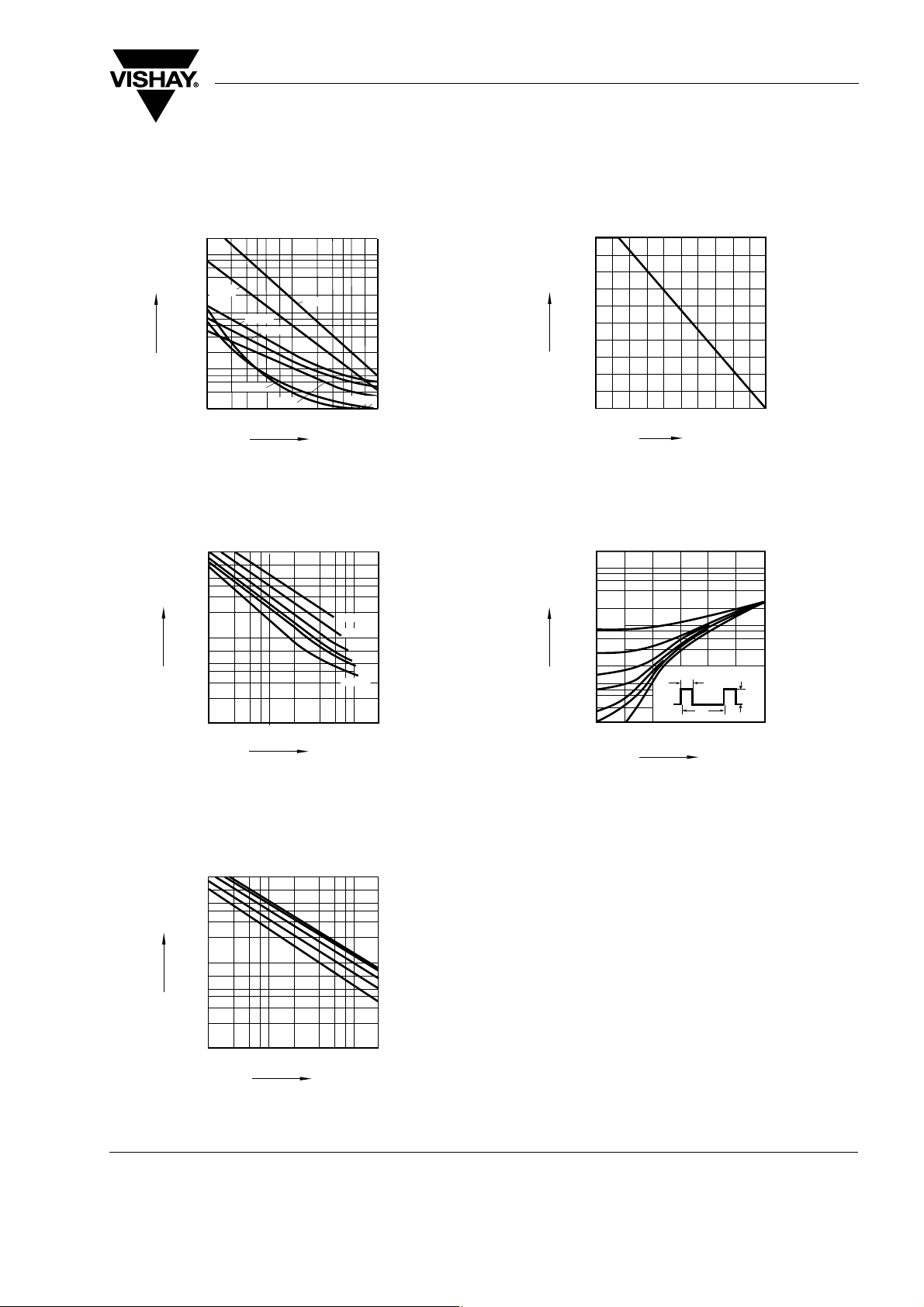
Typical Characteristics
T
= 25 °C, unless otherwise specified
amb
ZMY3V9 to ZMY100
Vishay Semiconductors
Ω
3
10
5
4
3
2
r
zj
18312
ZMY5.1
2
10
5
4
3
2
10
5
4
3
2
1
ZMY18
ZMY6.2
3254
1
2
ZMY12
ZMY10
10 100 mA
54
7
ZMY4.3
I
ZMY...
ZMY7.5
3
7
Z
Figure 1. Dynamic Resistance vs. Zener Current
Ω
100
7
5
4
3
r
zj
2
10
7
5
4
3
2
1
10 100 mA
3254
1
18313
54
2
ZMY...
ZMY43
ZMY36
ZMY30
ZMY24
ZMY22
ZMY18
3
I
Z
Figure 2. Dynamic Resistance vs. Zener Current
W
1.0
0.8
P
tot
ZMY...
0.6
0.4
0.2
0
0 100
19969
T
amb
200 °C
Figure 4. Admissible Power Dissipation vs. Ambient Temperature
°C/W
3
10
5
4
3
2
r
thA
2
10
5
0.5
4
3
0.2
2
10
0.1
5
4
3
2
1
10-510-410
18286
0.02
0.05
0.01
V = 0
t
P
-3
10-210-1110 s
v =
ZMY...
t
P
___
P
I
T
T
t
P
Figure 5. Pulse Thermal Resistance vs. Pulse Duration
Ω
3
10
7
5
4
3
r
zj
2
2
10
7
5
4
3
2
10
0.1
2
18314
Figure 3. Dynamic Resistance vs. Zener Current
Document Number 85788
Rev. 1.7, 07-Aug-06
ZMY...
110
3254
54
3
I
Z
ZMY100
ZMY82
ZMY68
ZMY56
ZMY43
mA
www.vishay.com
3

ZMY3V9 to ZMY100
Vishay Semiconductors
mA
240
ZMY3.9
200
I
Z
160
120
Test Current l
100 mA
Z
80
40
0
01234567
18309
Figure 6. Breakdown Characteristics
mA
60
ZMY15
50
I
Z
40
Test Current l
25 mA
30
20
10
Z
ZMY4.7
ZMY5.6
ZMY6.8
ZMY8.2
ZMY10
50 mA
8 9 1011 12131415 V
V
Z
ZMY18
ZMY22
ZMY27
ZMY33
10 mA
ZMY...
Tj = 25 °C
ZMY12
ZMY...
Tj = 25 °C
ZMY39
ZMY47
mA
20
I
Z
Test Current l
10 mA
Z
10
0
0 100
18311
50
Figure 8. Breakdown Characteristics
ZMY56
ZMY68
ZMY82
ZMY100
5 mA
ZMY...
Tj = 25 °C
150
V
Z
200 V
0
0 5 101520253035
18310
V
Figure 7. Breakdown Characteristics
40 45 50 V
Z
www.vishay.com
4
Document Number 85788
Rev. 1.7, 07-Aug-06

ZMY3V9 to ZMY100
Package Dimensions of MELF Glass in mm (Inches): DO41
Cathode Identification
Vishay Semiconductors
18317
Document Number 85788
Rev. 1.7, 07-Aug-06
www.vishay.com
5

ZMY3V9 to ZMY100
VISHAY
Vishay Semiconductors
Ozone Depleting Substances Policy Statement
It is the policy of Vishay Semiconductor GmbH to
1. Meet all present and future national and international statutory requirements.
2. Regularly and continuously improve the performance of our products, processes, distribution and operating
systems with respect to their impact on the health and safety of our employees and the public, as well as
their impact on the environment.
It is particular concern to control or eliminate releases of those substances into the atmosphere which are
known as ozone depleting substances (ODSs).
The Montreal Protocol (1987) and its London Amendments (1990) intend to severely restrict the use of ODSs
and forbid their use within the next ten years. Various national and international initiatives are pressing for an
earlier ban on these substances.
Vishay Semiconductor GmbH has been able to use its policy of continuous improvements to eliminate the use
of ODSs listed in the following documents.
1. Annex A, B and list of transitional substances of the Montreal Protocol and the London Amendments
respectively
2. Class I and II ozone depleting substances in the Clean Air Act Amendments of 1990 by the Environmental
Protection Agency (EPA) in the USA
3. Council Decision 88/540/EEC and 91/690/EEC Annex A, B and C (transitional substances) respectively.
Vishay Semiconductor GmbH can certify that our semiconductors are not manufactured with ozone depleting
substances and do not contain such substances.
We reserve the right to make changes to improve technical design
and may do so without further notice.
Parameters can vary in different applications. All operating parameters must be validated for each
customer application by the customer. Should the buyer use Vishay Semiconductors products for any
unintended or unauthorized application, the buyer shall indemnify Vishay Semiconductors against all
claims, costs, damages, and expenses, arising out of, directly or indirectly, any claim of personal
damage, injury or death associated with such unintended or unauthorized use.
Vishay Semiconductor GmbH, P.O.B. 3535, D-74025 Heilbronn, Germany
www.vishay.com
6
Document Number 85788
Rev. 1.7, 07-Aug-06

Legal Disclaimer Notice
Vishay
Notice
Specifications of the products displayed herein are subject to change without notice. Vishay Intertechnology, Inc.,
or anyone on its behalf, assumes no responsibility or liability for any errors or inaccuracies.
Information contained herein is intended to provide a product description only. No license, express or implied, by
estoppel or otherwise, to any intellectual property rights is granted by this document. Except as provided in Vishay's
terms and conditions of sale for such products, Vishay assumes no liability whatsoever, and disclaims any express
or implied warranty, relating to sale and/or use of Vishay products including liability or warranties relating to fitness
for a particular purpose, merchantability, or infringement of any patent, copyright, or other intellectual property right.
The products shown herein are not designed for use in medical, life-saving, or life-sustaining applications.
Customers using or selling these products for use in such applications do so at their own risk and agree to fully
indemnify Vishay for any damages resulting from such improper use or sale.
Document Number: 91000 www.vishay.com
Revision: 08-Apr-05 1
 Loading...