

Vishay VS-VSKT105.. Series, VS-VSKH105.. Series, VS-VSKL105.. Series, VS-VSKN105.. Series DataSheet (Vishay)
VS-VSKT105.., VS-VSKH105.., VS-VSKL105.., VS-VSKN105.. Series
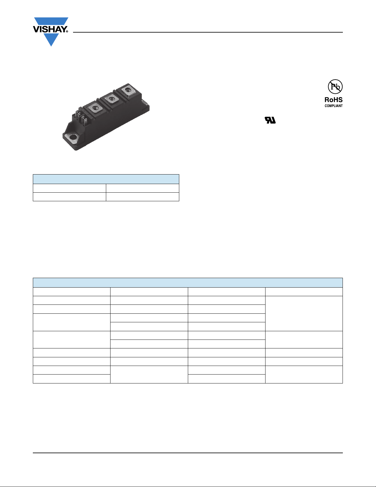
ADD-A-PAK
ADD-A-PAK Generation VII Power Modules
Thyristor/Diode and Thyristor/Thyristor, 105 A
PRODUCT SUMMARY
I
or I
T(AV)
F(AV)
Type Modules - Thyristor, Standard
MECHANICAL DESCRIPTION
The ADD-A-PAK Generation VII, new generation of
ADD-A-PAK module, combines the excellent thermal
performances obtained by the usage of exposed direct
bonded copper substrate, with advanced compact simple
package solution and simplified internal structure with
minimized number of interfaces.
105 A
Vishay Semiconductors
FEATURES
• High voltage
• Industrial standard package
• Low thermal resistance
• UL approved file E78996
• Designed and qualified for industrial level
BENEFITS
• Excellent thermal performances obtained by the usage of
exposed direct bonded copper substrate
• Up to 1600 V
• High surge capability
• Easy mounting on heatsink
ELECTRICAL DESCRIPTION
These modules are intended for general purpose high
voltage applications such as high voltage regulated power
supplies, lighting circuits, temperature and motor speed
control circuits, UPS and battery charger.
MAJOR RATINGS AND CHARACTERISTICS
SYMBOL CHARACTERISTICS VALUES UNITS
I
or I
T(AV)
F(AV)
I
O(RMS)
I
TSM,
I
FSM
2
I
t
2
I
t 200 kA2s
V
RRM
T
Stg
T
J
Revision: 21-Mar-14
85 °C 105
As AC switch 235
50 Hz 2000
60 Hz 2094
50 Hz 20
60 Hz 18.26
Range 400 to 1600 V
-40 to 130
-40 to 130
1
Document Number: 94628
A
kA2s
°C
VS-VSKT105.., VS-VSKH105.., VS-VSKL105.., VS-VSKN105.. Series
Vishay Semiconductors
ELECTRICAL SPECIFICATIONS
VOLTAGE RATINGS
V
, MAXIMUM
RRM
REPETITIVE PEAK
REVERSE VOLTAGE
TYPE NUMBER
VOLTAGE
CODE
V
04 400 500 400
06 600 700 600
08 800 900 800
VS-VSK.105
10 1000 1100 1000
12 1200 1300 1200
14 1400 1500 1400
16 1600 1700 1600
ON-STATE CONDUCTION
PARAMETER SYMBOL TEST CONDITIONS VALUES UNITS
Maximum average on-state current (thyristors) I
Maximum average forward current (diodes) I
T(AV)
F(AV)
V
, MAXIMUM
RSM
NON-REPETITIVE PEAK
V
REVERSE VOLTAGE
V
180° conduction, half sine wave,
= 85 °C
T
C
, MAXIMUM REPETITIVE
DRM
PEAK OFF-STATE VOLTAGE,
GATE OPEN CIRCUIT
V
105
I
RRM, IDRM
AT 130 °C
mA
20
Maximum continuous RMS on-state current,
as AC switch
Maximum peak, one-cycle non-repetitive
on-state or forward current
Maximum I
Maximum I
2
t for fusing I2t
2
t for fusing I2t
Maximum value or threshold voltage V
Maximum value of on-state
slope resistance
Maximum peak on-state or forward voltage
Maximum non-repetitive rate of rise of
turned on current
Maximum holding current I
Maximum latching current I
Notes
(1)I2
t for time tx = I2t x t
(2)
Average power = V
(3)
16.7 % x x IAV < I < x I
(4)
I > x I
AV
T(TO)
x
x I
T(AV)
AV
+ rt x (I
T(RMS)
2
)
I
O(RMS)
I
TSM
or
I
FSM
T(TO)
r
t
V
TM
V
FM
dI/dt
H
L
or
I
(RMS)
t = 10 ms
t = 8.3 ms 2094
t = 10 ms
t = 8.3 ms 1760
t = 10 ms
t = 8.3 ms 18.26
t = 10 ms
t = 8.3 ms 12.91
t = 0.1 ms to 10 ms, no voltage reapplied
(1)
T
= TJ maximum
J
Low level
(2)
High level
Low level
(2)
High level
ITM = x I
IFM = x I
T
= 25 °C, from 0.67 V
J
I
= x I
TM
No voltage
reapplied
Sinusoidal
half wave,
100 % V
RRM
initial T
reapplied
No voltage
reapplied
Initial TJ = TJ maximum
100 % V
RRM
reapplied
(3)
TJ = TJ maximum
(4)
(3)
TJ = TJ maximum
(4)
T(AV)
TJ = 25 °C 1.8 V
F(AV)
,
, Ig = 500 mA, tr < 0.5 μs, tp > 6 μs
T(AV)
DRM
I
(RMS)
= TJ maximum
J
TJ = 25 °C, anode supply = 6 V,
resistive load, gate open circuit
TJ = 25 °C, anode supply = 6 V, resistive load 400
235
2000
1682
20
14.14
kA2s
200 kA
0.98
1.12
2.7
2.34
m
150 A/μs
250
mA
A
2
s
V
Revision: 21-Mar-14
2
Document Number: 94628
VS-VSKT105.., VS-VSKH105.., VS-VSKL105.., VS-VSKN105.. Series
Vishay Semiconductors
TRIGGERING
PARAMETER SYMBOL TEST CONDITIONS VALUES UNITS
Maximum peak gate power P
Maximum average gate power P
Maximum peak gate current I
Maximum peak negative gate voltage - V
GM
G(AV)
GM
GM
TJ = -40 °C
Maximum gate voltage required to trigger V
GT
T
= 25 °C 2.5
J
T
= 125 °C 1.7
J
Anode supply = 6 V
resistive load
TJ = -40 °C
Maximum gate current required to trigger I
Maximum gate voltage that will not trigger V
Maximum gate current that will not trigger I
GD
GT
T
TJ = 125 °C, rated V
GD
TJ = 125 °C, rated V
= 25 °C 150
J
= 125 °C 80
J
Anode supply = 6 V
resistive load
applied 0.25 V
DRM
applied 6 mA
DRM
BLOCKING
PARAMETER SYMBOL TEST CONDITIONS VALUES UNITS
Maximum peak reverse and off-state
leakage current at V
RRM
, V
DRM
Maximum RMS insulation voltage V
Maximum critical rate of rise of off-state voltage dV/dt T
I
RRM,
I
DRM
INS
TJ = 130 °C, gate open circuit 20 mA
50 Hz
= 130 °C, linear to 0.67 V
J
DRM
12
3
W
3A
10
4.0
V
270
mAT
3000 (1 min)
3600 (1 s)
V
1000 V/μs
THERMAL AND MECHANICAL SPECIFICATIONS
PARAMETER SYMBOL TEST CONDITIONS VALUES UNITS
Junction operating temperature range T
Storage temperature range T
Maximum internal thermal resistance,
junction to case per leg
Typical thermal resistance,
case to heatsink per module
to heatsink
Mounting torque ± 10 %
busbar 3
Approximate weight
Case style JEDEC
R
R
J
Stg
thJC
thCS
-40 to 130 °C
DC operation 0.22
Mounting surface flat, smooth and greased 0.1
A mounting compound is recommended and
the torque should be rechecked after a period
4
of 3 hours to allow for the spread of the
compound.
75 g
2.7 oz.
®
AAP GEN VII (TO-240AA)
°C/W
Nm
R CONDUCTION PER JUNCTION
DEVICES
VSK.105.. 0.04 0.048 0.063 0.085 0.125 0.033 0.052 0.067 0.088 0.127 °C/W
Note
• Table shows the increment of thermal resistance R
SINE HALF WAVE CONDUCTION RECTANGULAR WAVE CONDUCTION
180° 120° 90° 60° 30° 180° 120° 90° 60° 30°
when devices operate at different conduction angles than DC
thJC
UNITS
Revision: 21-Mar-14
3
Document Number: 94628

VS-VSKT105.., VS-VSKH105.., VS-VSKL105.., VS-VSKN105.. Series
Average on-state current (A)
Maximum allowable case temperature (°C)
0 20406080100120
70
80
90
100
110
120
130
180°
120°
90°
60°
30°
RthJC (DC) = 0.22°C/W
0 20406080100120140160180
70
80
90
100
110
120
130
180°
120°
90°
60°
30°
DC
RthJC (DC) = 0.22°C/W
Average on-state current (A)
Maximum allowable case temperature (°C)
Average on-state current (A)
Maximum average on-state power loss (W)
020406080100120
0
20
40
60
80
100
120
140
160
180
200
180°
120°
90°
60°
30°
RMS limit
Per leg, Tj = 130°C
Vishay Semiconductors
Fig. 1 - Current Ratings Characteristics
260
240
220
200
180
180°
120°
90°
60°
30°
160
140
RMS limit
120
100
80
60
40
20
0
Maximum average on-state power loss (W)
Per leg, Tj = 130°C
0 20406080100120140160180
Average on-state current (A)
Fig. 4 - On-State Power Loss Characteristics
1800
At any rated load condition and with
rated Vrrm app lied following surge
1600
Initial Tj = Tj max
@ 60 Hz 0.0083 s
@ 50 Hz 0.0100s
1400
DC
Fig. 2 - Current Ratings Characteristics
Revision: 21-Mar-14
Fig. 3 - On-State Power Loss Characteristics
1200
1000
Per leg
Peak half sine wave on-state current (A)
800
110100
Number of equal amplitude half cycle current pulses (N)
Fig. 5 - Maximum Non-Repetitive Surge Current
2000
Maximum Non-repetitive Surge Current
1800
1600
Versus Pulse Train Duration. Control
of conduction may not be maintained.
Initial T j = 130°C
No Voltage Reapplied
Rated Vrrm reapplied
1400
1200
1000
Peak half sine wave on-state current (A)
Per leg
800
0.01 0.1 1
Pulse train duration (s)
Fig. 6 - Maximum Non-Repetitive Surge Current
4
Document Number: 94628

VS-VSKT105.., VS-VSKH105.., VS-VSKL105.., VS-VSKN105.. Series
Total output current (A)
Maximum allowable ambient temperature (°C)
Maximum total power loss (W)
0 20 40 60 80 100 120 140
RthSA = 0.1 °C/W
0.2 °C/W
0.3 °C/W
0.5 °C/W
1 °C/W
0 40 80 120 160 200 240
0
100
200
300
400
500
600
700
800
900
120°
(rect)
3 x VSK.105 Series
three phase brid ge connected
Tj = 130°C
Vishay Semiconductors
400
350
300
250
180°
120°
90°
60°
30°
200
150
100
50
Maximum total on-state power loss (W)
0
0 40 80 120 160 200 240
Total RMS output current (A)
Fig. 7 - On-State Power Loss Characteristics
700
180°
600
500
400
∼
(sine)
180°
(rect)
300
RthSA = 0.1 °C/W
0.2 °C/W
0.3 °C/W
0.5 °C/W
0.7 °C/W
1 °C/W
2°C/W
VSK.105 Series
Per module
Tj = 130°C
0 20 40 60 80 100 120 140
Maximum allowable ambient temperature (°C)
RthSA = 0.1 °C/W
0.2 °C/W
0.3 °C/W
0.5 °C/W
0.7 °C/W
1 °C/W
2 °C/W
Revision: 21-Mar-14
Maximum total power loss (W)
200
100
2 x VSK.105 Series
single phase bridge connected
Tj = 130°C
0
0 40 80 120 160 200
Total output current (A)
Fig. 8 - On-State Power Loss Characteristics
Fig. 9 - On-State Power Loss Characteristics
0 20 40 60 80 100 120 140
Maximum allowable ambient temperature (°C)
5
Document Number: 94628

VS-VSKT105.., VS-VSKH105.., VS-VSKL105.., VS-VSKN105.. Series
Vishay Semiconductors
1000
Per leg
100
10
Tj = 130°C
Instantaneous on-state current (A)
1
0.5 1.0 1.5 2.0 2.5 3.0 3.5
Instantaneous on-state voltage (V)
Fig. 10 - On-State Voltage Drop Characteristics
1
Tj = 25°C
(°C/W)
thJC
Steady state value
RthJC = 0.22 °C/W
(DC operation)
0.1
0.01
Per leg
0.001
Transient thermal impedance Z
0.001 0.01 0.1 1 10
Square wave pulse duration (s)
Fig. 11 - Thermal Impedance Z
100
Rectangular gate pulse
a)Recommended load line for
rated di/dt: 20 V, 20 ohms
tr = 0.5 µs, tp >= 6 µs
b)Recommended load line for
<= 30% rated di/dt: 15 V, 40 ohms
tr = 1 µs, tp >= 6 µs
10
1
Instantaneous gate voltage (V)
VGD
IGD
0.1
0.001 0.01 0.1 1 10 100 1000
(a)
(b)
TJ = - 40 ° C
TJ = 25 ° C
TJ = 1 2 5 ° C
IRK.105.. Series
VSK.
Instantaneous gate current (A)
Characteristics
thJC
(1) PGM = 200 W, tp = 300 µs
(2) PGM = 60 W, t p = 1 ms
(3) PGM = 30 W, t p = 2 ms
(4) PGM = 12 W, t p = 5 ms
(3)
(4)
Frequency Limited by PG(AV)
(2) (1)
Fig. 12 - Gate Characteristics
Revision: 21-Mar-14
6
Document Number: 94628

VS-VSKT105.., VS-VSKH105.., VS-VSKL105.., VS-VSKN105.. Series
2 - Module type
1 - Vishay Semiconductors product
3
4
- Current code (105 A)
5 - Voltage code (see Voltage Ratings table)
Device code
2
1
43 5
KVS-VS T 105 / 16
- Circuit configuration (see Circuit Configuration table)
+
-
K1
(5)K2(7)G2(6)
G1
(4)
~
(1)
(2)
(3)
VSKT
1
2
3
4 5 7 6
+
-
K2
(7)G2(6)
~
(1)
(2)
(3)
VSKL
1
2
3
7 6
+
+
K1
(5)G1(4)
-
(1)
(2)
(3)
VSKN
1
2
3
4 5
Vishay Semiconductors
ORDERING INFORMATION TABLE
CIRCUIT CONFIGURATION
CIRCUIT DESCRIPTION CIRCUIT CONFIGURATION CODE CIRCUIT DRAWING
Two SCRs doubler circuit T
SCR/diode doubler circuit,
positive control
SCR/diode doubler circuit,
negative control
(1)
~
1
VSKH
H
2
3
4 5
+
(2)
-
(3)
K1
(5)G1(4)
L
SCR/diode common anodes N
Revision: 21-Mar-14
7
Document Number: 94628

Legal Disclaimer Notice
Vishay
Disclaimer
ALL PRODUCT, PRODUCT SPECIFICATIONS AND DATA ARE SUBJECT TO CHANGE WITHOUT NOTICE TO IMPROVE
RELIABILITY, FUNCTION OR DESIGN OR OTHERWISE.
Vishay Intertechnology, Inc., its affiliates, agents, and employees, and all persons acting on its or their behalf (collectively,
“Vishay”), disclaim any and all liability for any errors, inaccuracies or incompleteness contained in any datasheet or in any other
disclosure relating to any product.
Vishay makes no warranty, representation or guarantee regarding the suitability of the products for any particular purpose or
the continuing production of any product. To the maximum extent permitted by applicable law, Vishay disclaims (i) any and all
liability arising out of the application or use of any product, (ii) any and all liability, including without limitation special,
consequential or incidental damages, and (iii) any and all implied warranties, including warranties of fitness for particular
purpose, non-infringement and merchantability.
Statements regarding the suitability of products for certain types of applications are based on Vishay’s knowledge of
typical requirements that are often placed on Vishay products in generic applications. Such statements are not binding
statements about the suitability of products for a particular application. It is the customer’s responsibility to validate that a
particular product with the properties described in the product specification is suitable for use in a particular application.
Parameters provided in datasheets and / or specifications may vary in different applications and performance may vary over
time. All operating parameters, including typical parameters, must be validated for each customer application by the customer’s
technical experts. Product specifications do not expand or otherwise modify Vishay’s terms and conditions of purchase,
including but not limited to the warranty expressed therein.
Except as expressly indicated in writing, Vishay products are not designed for use in medical, life-saving, or life-sustaining
applications or for any other application in which the failure of the Vishay product could result in personal injury or death.
Customers using or selling Vishay products not expressly indicated for use in such applications do so at their own risk.
Please contact authorized Vishay personnel to obtain written terms and conditions regarding products designed for
such applications.
No license, express or implied, by estoppel or otherwise, to any intellectual property rights is granted by this document
or by any conduct of Vishay. Product names and markings noted herein may be trademarks of their respective owners.
© 2017 VISHAY INTERTECHNOLOGY, INC. ALL RIGHTS RESERVED
Revision: 08-Feb-17
1
Document Number: 91000
 Loading...