VS-VSK.250PbF, VS-VSK.270PbF, VS-VSK.320PbF Series
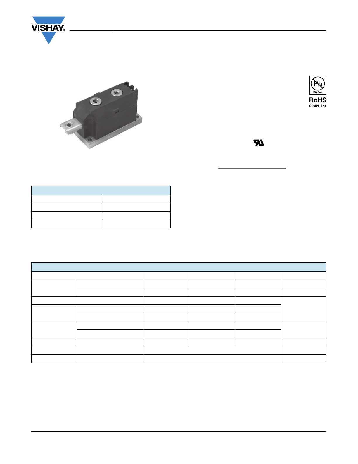
MAGN-A-PAK
Standard Recovery Diodes, 250 A to 320 A
PRODUCT SUMMARY
I
F(AV)
Type Modules - Diode, High Voltage
Package MAGN-A-PAK
Circuit Two diodes doubler circuit
Vishay Semiconductors
(MAGN-A-PAK Power Modules)
FEATURES
• High voltage
• Electrically isolated base plate
250 A to 320 A
• 3000 V
• Industrial standard package
• Simplified mechanical designs, rapid assembly
• High surge capability
• Large creepage distances
• UL approved file E78996
• Designed and qualified for industrial level
• Material categorization: for definitions of compliance
please see www.vishay.com/doc?99912
DESCRIPTION
This new VS-VSK series of MAGN-A-PAKs uses
high voltage power diodes in two basic configurations. The
semiconductors are electrically isolated from the metal
base, allowing common heatsinks and compact assemblies
to be built. They can be interconnected to form single phase
or three phase bridges and the single diode module can be
used in conjunction with the thyristor modules as a
freewheel diode. These modules are intended for general
purpose applications such as battery chargers, welders and
plating equipment and where high voltage and high current
are required (motor drives, etc.).
isolating voltage
RMS
MAJOR RATINGS AND CHARACTERISTICS
SYMBOL CHARACTERISTICS VSK.250.. VSK.270.. VSK.320.. UNITS
I
F(AV)
I
F(RMS)
I
FSM
2
t
I
2
I
t 2460 3980 5110 kA2s
V
RRM
T
J
Revision: 28-May-14
T
C
50 Hz 7015 8920 10 110
60 Hz 7345 9430 10 580
50 Hz 246 398 511
60 Hz 225 363 466
250 270 320 A
100 100 100 °C
393 424 502
400 to 3000 V
-40 to +150 °C
1
Document Number: 93581
A
kA2s

VS-VSK.250PbF, VS-VSK.270PbF, VS-VSK.320PbF Series
Vishay Semiconductors
ELECTRICAL SPECIFICATIONS
VOLTAGE RATINGS
V
MAXIMUM REPETITIVE
TYPE NUMBER
VOLTAGE
CODE
RRM,
PEAK REVERSE VOLTAGE
V
04 400 500
VS-VSK.250
VS-VSK.270
VS-VSK.320
08 800 900
12 1200 1300
16 1600 1700
20 2000 2100
VS-VSK.270 30 3000 3100
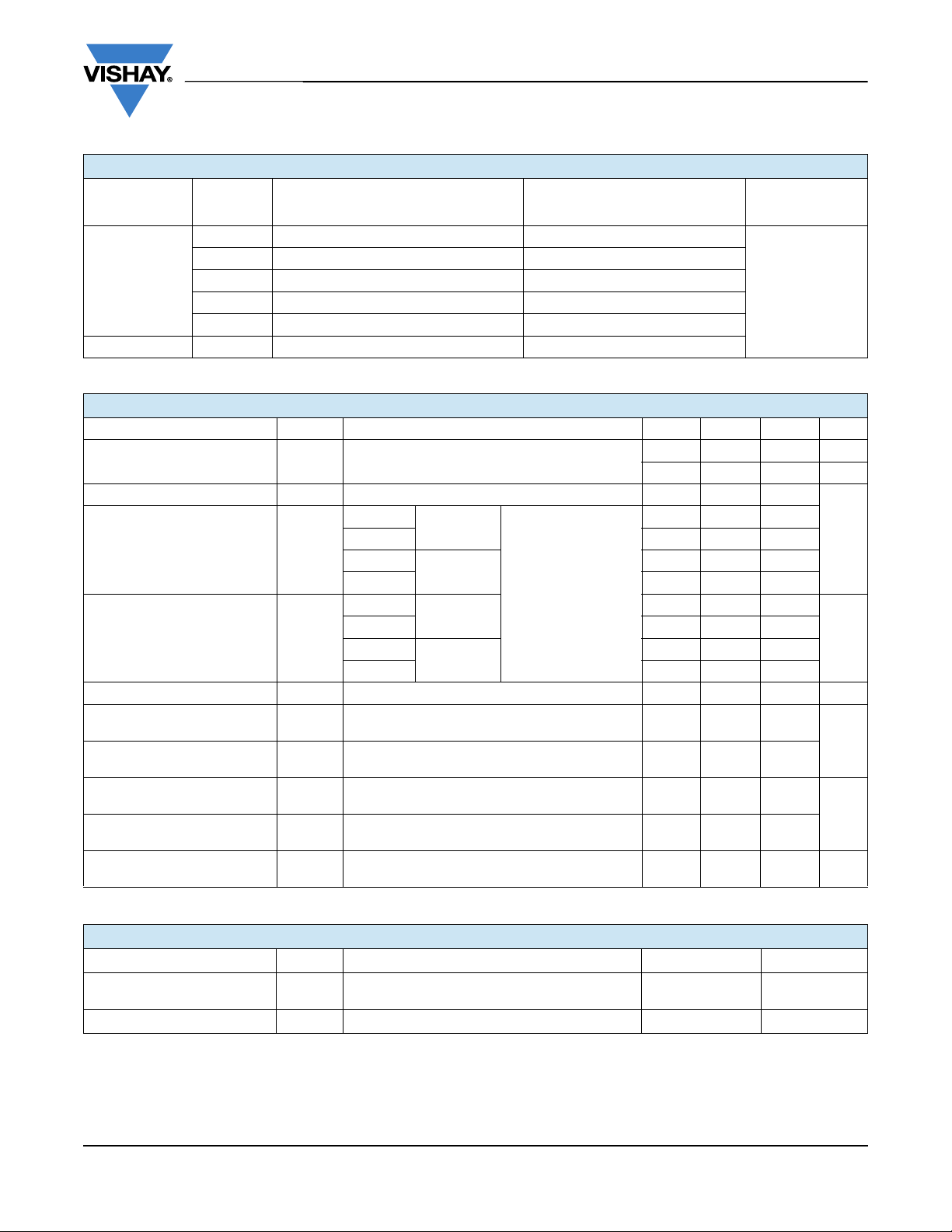
FORWARD CONDUCTION
PARAMETER SYMBOL TEST CONDITIONS VSK.250 VSK.270 VSK.320 UNITS
Maximum average forward
current at case temperature
Maximum RMS forward current I
Maximum peak, one-cycle
forward, non-repetitive
surge current
Maximum I
Maximum I
2
t for fusing I2t
2
t for fusing I2t t = 0.1 ms to 10 ms, no voltage reapplied 2460 3980 5110 kA2s
Low level value of
threshold voltage
High level value of
threshold voltage
Low level forward
slope resistance
High level forward
slope resistance
Maximum forward voltage drop V
I
F(AV)
F(RMS)
I
FSM
V
F(TO)1
V
F(TO)2
r
f1
r
(I > x I
f2
FM
180° conduction, half sine wave
As AC switch 393 424 502
t = 10 ms
t = 8.3 ms 7345 9340 10 580
t = 10 ms
t = 8.3 ms 6180 7850 8900
t = 10 ms
t = 8.3 ms 225 363 466
t = 10 ms
t = 8.3 ms 159 257 330
(16.7 % x x I
T
= TJ maximum
J
(I > x I
(16.7 % x x I
= TJ maximum
T
J
IFM = x I
Average power = V
No voltage
reapplied
100 % V
RRM
reapplied
No voltage
reapplied
100 % V
RRM
reapplied
< I < x I
F(AV)
), TJ = TJ maximum 0.92 0.87 0.86
F(AV)
< I < x I
F(AV)
), TJ = TJ maximum 0.49 0.81 0.44
F(AV)
, TJ = TJ maximum, 180° conduction
F(AV)
F(TO)
x I
V
, MAXIMUM NON-REPETITIVE
RSM
PEAK REVERSE VOLTAGE
Sinusoidal half wave,
initial T
= TJ maximum
J
),
F(AV)
),
F(AV)
+ rf x (I
F(AV)
F(RMS)
I
MAXIMUM
RRM
V
AT 150 °C
mA
50
250 270 320 A
100 100 100 °C
7015 8920 10 110
5900 7500 8500
246 398 511
174 281 361
0.79 0.74 0.69
0.63 0.94 0.59
2
)
1.29 1.48 1.28 V
A
kA2s
V
m
BLOCKING
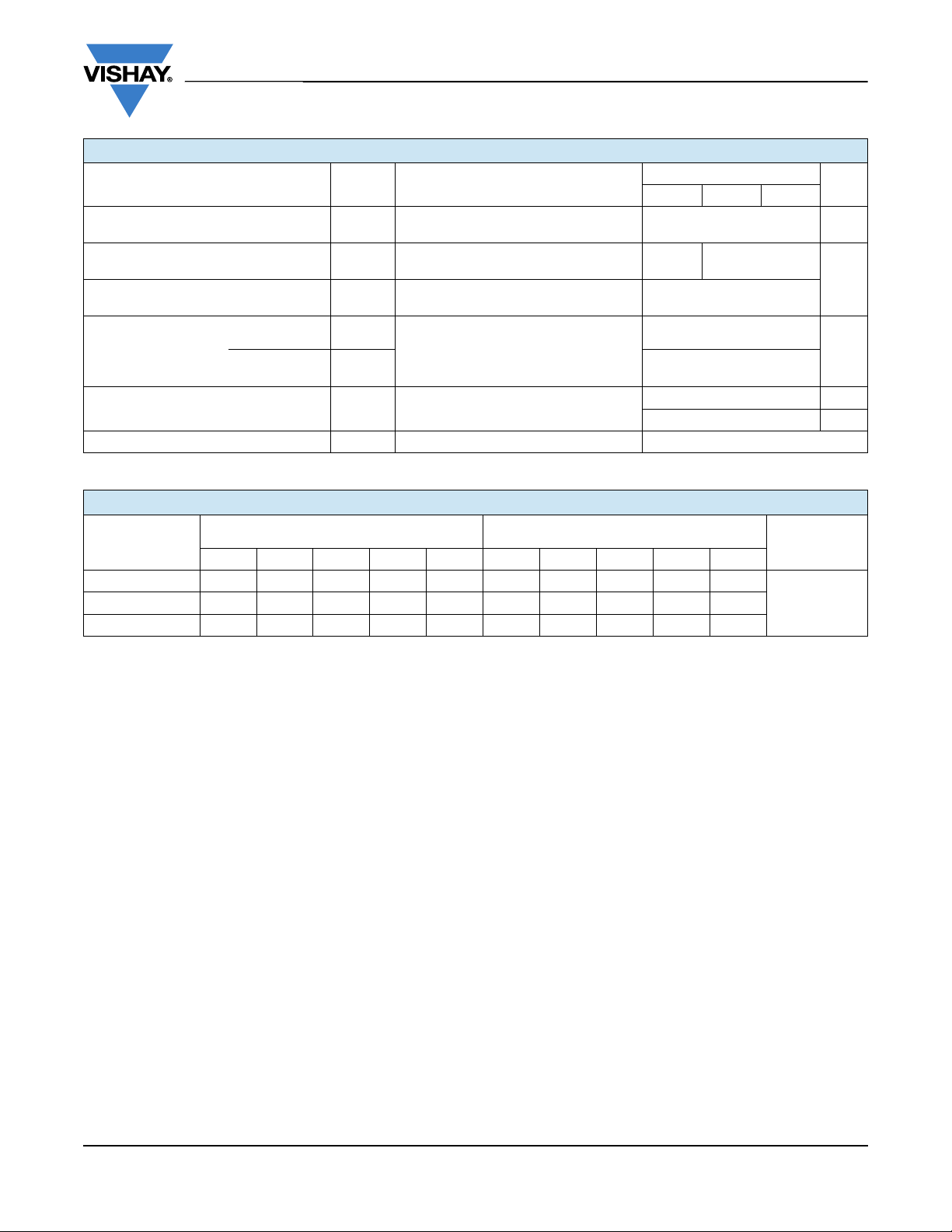
PARAMETER SYMBOL TEST CONDITIONS VALUES UNITS
Maximum peak reverse
leakage current
RMS insulation voltage V
Revision: 28-May-14
I
RRM
INS
TJ = 150 °C 50 mA
50 Hz, circuit to base, all terminals shorted, t = 1 s 3000 V
2
Document Number: 93581

VS-VSK.250PbF, VS-VSK.270PbF, VS-VSK.320PbF Series
Vishay Semiconductors
THERMAL AND MECHANICAL SPECIFICATIONS
PARAMETER SYMBOL TEST CONDITIONS
Maximum junction operating and storage
temperature range
Maximum thermal resistance,
junction to case per junction
Maximum resistance, case to heatsink
per module
Mounting torque
± 10 %
Approximate weight
Case style MAGN-A-PAK
MAP to heatsink
busbar to MAP 8 to 10
T
, T
J
Stg
DC operation 0.16 0.125
Mounting surface flat, smooth and
greased
A mounting compound is recommended
and the torque should be rechecked
after a period of about 3 hours to allow for
the spread of the compound.
R
R
thJC
thCS
VSK.250 VSK.270 VSK.320
R CONDUCTION PER JUNCTION
SINUSOIDAL CONDUCTION
DEVICE
180° 120° 90° 60° 30° 180° 120° 90° 60° 30°
VSK.250 0.009 0.010 0.014 0.020 0.032 0.007 0.011 0.015 0.021 0.033
VSK.320 0.008 0.010 0.013 0.020 0.032 0.007 0.011 0.015 0.020 0.033
Note
• The table above shows the increment of thermal resistance R
AT T
MAXIMUM
J
when devices operate at different conduction angles than DC
thJC
RECTANGULAR CONDUCTION
AT TJ MAXIMUM
VALUES
-40 to +150 °C
0.035
4 to 6
800 g
30 oz.
UNITS
K/W
Nm
UNITS
K/WVSK.270 0.008 0.012 0.014 0.020 0.032 0.007 0.011 0.015 0.020 0.033
Revision: 28-May-14
3
Document Number: 93581

VS-VSK.250PbF, VS-VSK.270PbF, VS-VSK.320PbF Series
80
90
100
110
120
130
140
150
0 50 100 150 200 250 300 350 400
DC
30°
60°
90°
120°
180°
Maximu m Allow able C a se Tem perat ure (°C)
Conduction Period
Average Forward Current (A)
VSK.250 .. Se ri e s
R (DC) = 0.16 K/W
thJC
0
50
100
150
200
250
300
350
400
450
0 50 10 0 150 200 250 300 350 400
DC
180°
120°
90°
60°
30°
Average Forward Current (A)
RM S Li m i t
Maximum Average Forward Power Loss (W)
Conduction Period
VSK.250.. Series
T = 150°C
J
Vishay Semiconductors
150
140
VSK.250 .. Seri e s
R (DC) = 0.16 K/W
thJC
130
120
Conduction Angle
110
100
90
80
Maximum Allowable Case Temperature (°C)
0 50 100 150 200 250 300
30°
60°
90°
120°
Average Forward Current (A)
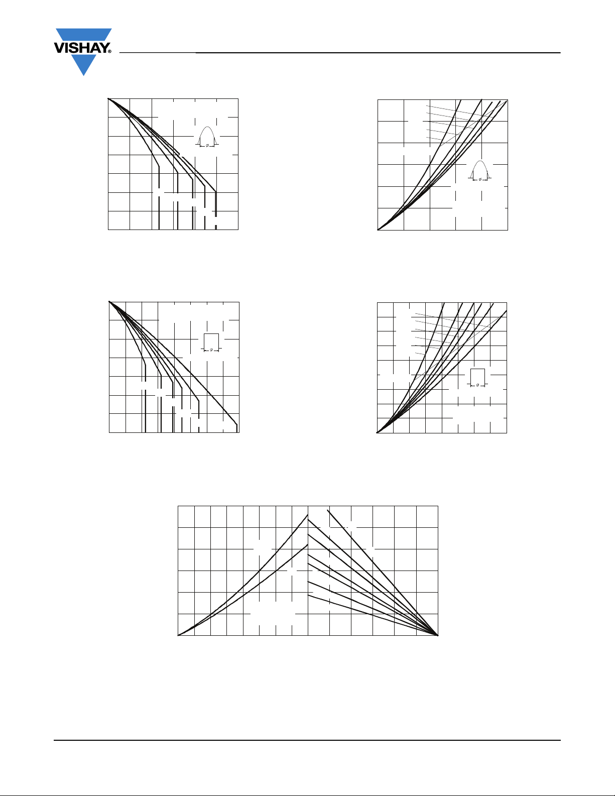
Fig. 1 - Current Ratings Characteristics
180°
300
250
200
180°
120°
90°
60°
30°
RM S Lim it
150
100
50
0
Maximum Ave rage Forward Power Loss (W)
0 50 100 150 200 250
Cond uct ion An gle
VSK.250.. Series
T = 15 0° C
J
Ave rag e Forw ard Curre nt (A)
Fig. 3 - Forward Power Loss Characteristics
Fig. 2 - Current Ratings Characteristics
Revision: 28-May-14
600
500
400
180°
(Sine)
300
200
VSK.25 0.. Se ri e s
100
Maximum Total Forward Power Loss (W)
0
0 50 100 150 200 250 3 00 3 50 400
Pe r Ju nc t io n
T = 15 0° C
J
Total RMS Output Current (A)
Fig. 5 - Forward Power Loss Characteristics
Fig. 4 - Forward Power Loss Characteristics
R
t
h
S
A
0
.
0
=
8
0
K
0
/
.
0
W
2
K
W
W
W
W
/
W
D
e
l
t
a
R
DC
.
1
2
K
/
0
.
2
K
/
0
.
2
5
K
/
0
.
4
K
/
0
.
6
K
/
W
0 25 50 75 100 125 150
Maximum Allowable Ambient Temperature (°C)
4
Document Number: 93581
 Loading...