

(SUPER MAGN-A-PAK Power Modules)
SUPER MAGN-A-PAK
PRODUCT SUMMARY
I
F(AV)
Type Modules - Diode, High Voltage
Standard Diodes, 600 A
FEATURES
• High current capability
• High surge capability
• High voltage ratings up to 2000 V
600 A
• 3000 V
• Industrial standard package
• UL approved file E78996
• Compliant to RoHS directive 2002/95/EC
TYPICAL APPLICATIONS
• Rectifying bridge for large motor drives
• Rectifying bridge for large UPS
isolating voltage with non-toxic substrate
RMS
VSKD600 Series
Vishay Semiconductors
MAJOR RATINGS AND CHARACTERISTICS
SYMBOL CHARACTERISTICS VALUES UNITS
I
F(AV)
I
F(RMS)
I
FSM
2
I
t
2
I
t 18 050 kA2s
V
RRM
, T
T
Stg
J
T
C
T
C
50 Hz 19 000
60 Hz 20 100
50 Hz 1805
60 Hz 1683
Range 800 to 2000 V
Range - 40 to 150 °C
600 A
100 °C
942 A
100 °C
ELECTRICAL SPECIFICATIONS
VOLTAGE RATINGS
V
TYPE NUMBER
VSKD600..
, MAXIMUM REPETITIVE
VOLTAGE
CODE
08 800 900
12 1200 1300
16 1600 1700
20 2000 2100
RRM
PEAK REVERSE VOLTAGE
V
V
, MAXIMUM NON-REPETITIVE
RSM
PEAK REVERSE VOLTAGE
V
I
AT T
A
kA2s
MAXIMUM
RRM
MAXIMUM
J
mA
50
Document Number: 93583 For technical questions within your region, please contact one of the following: www.vishay.com
Revision: 02-Jul-10 DiodesAmericas@vishay.com
, DiodesAsia@vishay.com, DiodesEurope@vishay.com 1
VSKD600 Series
Vishay Semiconductors
Standard Diodes, 600 A
(SUPER MAGN-A-PAK Power Modules)
FORWARD CONDUCTION
PARAMETER SYMBOL TEST CONDITIONS VALUES UNITS
Maximum average forward current
at case temperature
Maximum RMS forward current I
Maximum peak, one-cycle forward,
non-repetitive surge current
2
Maximum I
Maximum I
t for fusing I2t
2
t for fusing I2t t = 0.1 ms to 10 ms, no voltage reapplied 18 050 kA2s
Low level value of threshold voltage V
High level value of threshold voltage V
Low level value of forward slope resistance r
High level value of forward slope resistance r
Maximum forward voltage drop V
I
F(AV)
F(RMS)
180° conduction, half sine wave
180° conduction, half sine wave at TC = 100 °C 942 A
t = 10 ms
I
FSM
t = 8.3 ms 20.1
t = 10 ms
t = 8.3 ms 17.2
t = 10 ms
t = 8.3 ms 1683
t = 10 ms
t = 8.3 ms 1230
F(TO)1
F(TO)2
(16.7 % x x I
(I > x I
(16.7 % x x I
f1
(I > x I
f2
Ipk = 1800 A, TJ = 25 °C, tp = 10 ms sine pulse 1.45 V
FM
No voltage
reapplied
100 % V
reapplied
No voltage
RRM
Sinusoidal half wave,
initial T
= TJ maximum
J
reapplied
100 % V
RRM
reapplied
< I < x I
F(AV)
), TJ = TJ maximum 0.77
F(AV)
< I < x I
F(AV)
), TJ = TJ maximum 0.25
F(AV)
), TJ = TJ maximum 0.70
F(AV)
), TJ = TJ maximum 0.28
F(AV)
600 A
100 °C
19.0
16.2
1805
1319
kA
m
kA
2
s
V
BLOCKING
PARAMETER SYMBOL TEST CONDITIONS VALUES UNITS
RMS insulation voltage V
Maximum peak reverse and
off-state leakage current
I
RRM
INS
t = 1 s 3000 V
TJ = TJ maximum, rated V
applied 50 mA
RRM
THERMAL AND MECHANICAL SPECIFICATIONS
PARAMETER SYMBOL TEST CONDITIONS VALUES UNITS
Maximum junction operating and storage
temperature range
Maximum thermal resistance,
junction to case per junction
Maximum thermal resistance,
case to heatsink
Mounting torque
± 10 %
SMAP to heatsink
busbar to SMAP 12 to 15
Approximate weight 1500 g
Case style See dimensions - link at the end of datasheet SUPER MAGN-A-PAK
T
R
, T
J
R
thJC
thC-hs
Stg
DC operation 0.065
A mounting compound is recommended and the torque
should be rechecked after a period of 3 hours to allow
for the spread of the compound.
- 40 to 150 °C
K/W
0.02
6 to 8
Nm
www.vishay.com For technical questions within your region, please contact one of the following: Document Number: 93583
2 DiodesAmericas@vishay.com
, DiodesAsia@vishay.com, DiodesEurope@vishay.com Revision: 02-Jul-10
80
90
100
110
120
130
140
150
0 100 200 300 400 500 600 7
00
30°
60°
90°
120°
180°
Maximum Allowable Case Temperature (°C
)
Conduction Angle
Average Forward Curren t (A)
VSKD600.. Series
R (DC) = 0.065 K/W
thJC
80
90
100
110
120
130
140
150
0 200 400 600 800 10
00
DC
30°
60°
90°
120°
180°
Max imu m Allo wab le Case Temperat ure (°C
)
Conduction Period
Average Forward Current (A)
VSKD600.. Series
R (DC) = 0.065 K/W
thJC
0
100
200
300
400
500
600
700
0 100 200 300 400 500 600
Average Forward Current (A)
RMS Limit
Maximum Average Forward Power Loss (W)
Conduction Angle
180°
120°
90°
60°
30°
VSKD600.. Series
Per Junction
T = 150°C
J
0
100
200
300
400
500
600
700
800
900
1000
0 200 400 600 800 10
00
DC
180°
120°
90°
60°
30°
Average Forward Current (A)
RMS Limit
Maximum Average Forward Power Loss (W)
Conduction Perio d
VSKD600.. Series
Per Junction
T = 150°C
J
VSKD600 Series
Standard Diodes, 600 A
Vishay Semiconductors
(SUPER MAGN-A-PAK Power Modules)
R
CONDUCTION ANGLE SINUSOIDAL CONDUCTION RECTANGULAR CONDUCTION TEST CONDITIONS UNITS
Note
• The table above shows the increment of thermal resistance R
CONDUCTION
thJC
180° 0.009 0.006
120° 0.011 0.011
90° 0.014 0.015
60° 0.021 0.022
30° 0.037 0.038
when devices operate at different conduction angles than DC
thJC
= TJ maximum K/W
T
J
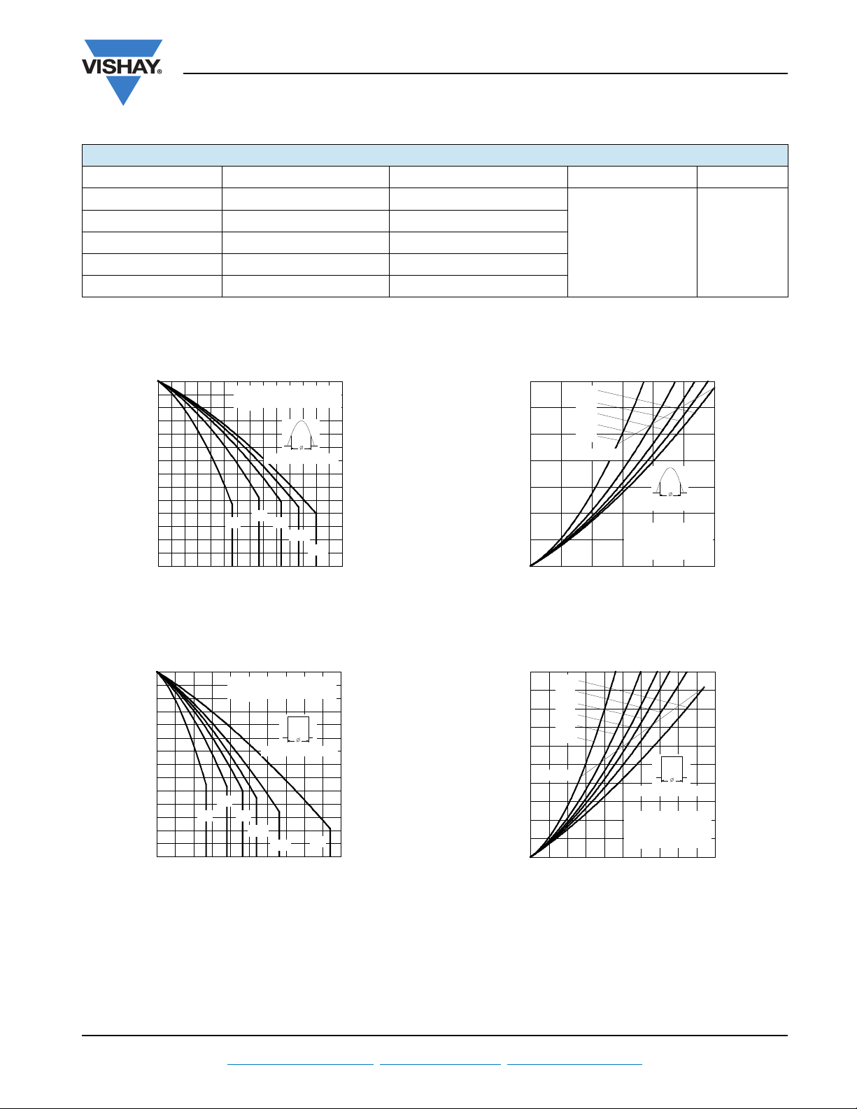
Fig. 1 - Current Ratings Characteristics
Document Number: 93583 For technical questions within your region, please contact one of the following: www.vishay.com
Revision: 02-Jul-10 DiodesAmericas@vishay.com
Fig. 2 - Current Ratings Characteristics
Fig. 3 - Forward Power Loss Characteristics
Fig. 4 - Forward Power Loss Characteristics
, DiodesAsia@vishay.com, DiodesEurope@vishay.com 3

VSKD600 Series
4000
6000
8000
10000
12000
14000
16000
18000
20000
0.01 0.1
1
Peak Half Sine Wave Forward Current (A)
Pulse Train Dur ation (s)
Maximum Non Repetitive Surge Curren t
Initial T = 150°C
No Voltage Reapplied
Rated V Reapplied
RRM
Versus Pulse Train Duration.
J
VSKD600.. Series
Per Junction
0 255075100125150
Maximum Allowable Ambient Temperature (°C)
R
=
0
.
0
2
K
/
W
D
e
l
t
a
R
th
S
A
0
.
0
4
K
/
W
0.
06
K
/W
0
.
0
8
K
/
W
0
.
1
2
K
/
W
0.
16
K
/
W
0
.
2
5
K
/
W
0
.
3
5
K
/
W
0
.
5
K
/
W
0
200
400
600
800
1000
0 200 400 600 800 1000
Total RMS Output Current (A)
Maximum Tot al Fo rward Powe r Loss (W)
VSKD600.. Series
Per Junction
T = 150°C
J
180°
(Sine)
DC
Vishay Semiconductors
18000
At Any Rated Load Condition And With
Rated V Applied Following Surge.
16000
14000
12000
10000
8000
6000
Peak Half Sine Wave Forward Current (A)
4000
110100
Number Of Equal Amplitude Half Cycle Current Pulses (N)
Fig. 5 - Maximum Non-Repetitive Surge Current Fig. 6 - Maximum Non-Repetitive Surge Current
RRM
VSKD600.. Series
Per Jun ction
Initial T = 150°C
@ 60 Hz 0.0083 s
@ 50 Hz 0.0100 s
Standard Diodes, 600 A
(SUPER MAGN-A-PAK Power Modules)
J
www.vishay.com For technical questions within your region, please contact one of the following: Document Number: 93583
4 DiodesAmericas@vishay.com
Fig. 7 - Forward Power Loss Characteristics
3000
2500
2000
180°
(Sine)
180°
(Rect)
1500
1000
2 x VSKD600.. Series
500
Maximum Total Power Loss (W)
0
0 200 400 600 800 1000 1200
Total Output Current (A)
Single Phase Bridge
Connected
T = 150°C
J
Fig. 8 - Forward Power Loss Characteristics
, DiodesAsia@vishay.com, DiodesEurope@vishay.com Revision: 02-Jul-10
R
0
t
.
0
h
2
0
.0
3 K
/
0
.
0
4
K
/
W
0
.
0
5
K
/
W
0
.
0
8
K
/
W
0
.
1
2
K
/
W
0
.
2
K
/
W
S
A
K
/
=
W
0
W
.
0
1
K
/
W
D
e
l
t
a
R
0 25 50 75 100 125 150
Maximum Allowable Ambient Temperature (°C)

VSKD600 Series
Standard Diodes, 600 A
(SUPER MAGN-A-PAK Power Modules)
4500
4000
3500
3000
2500
2000
1500
1000
Maximum Total Power Loss (W)
500
0
0 300 600 900 1200 1500 1800
Total Output Current (A)
)
thJ C
120°
(Rect )
3 x VSKD600.. Series
Three Phase Bridge
Connected
T = 150°C
J
Fig. 9 - Forward Power Loss Characteristics
0.1
VSKD600.. Series
Per Jun ction
Vishay Semiconductors
R
t
h
S
A
0
0
.
0
.
0
0
.
0
0
.
1
0
.
2
0255075100125150
Maximum Allowable Ambient Temperature (°C)
=
.
0
0
8
2
0
.
2
3
5
K
K
0
1
K
/
K
/
W
K
/
K
/
/
W
/
W
K
W
W
W
/
W
D
e
l
t
a
R
0.01
Steady State Value:
R = 0.065 K/W
thJC
(DC Operation)
Transient Thermal Impedance Z (K/W
0.001
0.001 0.01 0.1 1 10 100
Square Wave Pulse Duration ( s)
Fig. 10 - Thermal Impedance Z
thJC
Characteristic
Document Number: 93583 For technical questions within your region, please contact one of the following: www.vishay.com
Revision: 02-Jul-10 DiodesAmericas@vishay.com
, DiodesAsia@vishay.com, DiodesEurope@vishay.com 5

VSKD600 Series
+-
~
1
2
3
Vishay Semiconductors
Standard Diodes, 600 A
(SUPER MAGN-A-PAK Power Modules)
ORDERING INFORMATION TABLE
Device code
CIRCUIT CONFIGURATION
CIRCUIT DESCRIPTION
Two diodes doubler circuit D
VSK D 600 - 20
1324
1 - Module type
2 - Circuit configuration D = 2 diodes in series
(see Circuit Configuration table)
- Current rating
3
- Voltage code x 100 = V
4
CONFIGURATION CODE
CIRCUIT
(see Voltage Ratings table)
RRM
CIRCUIT DRAWING
LINKS TO RELATED DOCUMENTS
Dimensions www.vishay.com/doc?95088
www.vishay.com For technical questions within your region, please contact one of the following: Document Number: 93583
6 DiodesAmericas@vishay.com
, DiodesAsia@vishay.com, DiodesEurope@vishay.com Revision: 02-Jul-10

Super MAGN-A-PAK Diode
52 (2.05)
60.0 (2.36)
48.0 (1.89)
31.0
(1.22)
50.0
(1.97)
44.0
(1.73)
M10
Fast-on tabs
2.8 x 0.8 (0.11 x 0.03)
20.1
(0.78)
36.4 (1.14) 4.5 (0.20)
28.0
(1.10)
26.0
(0.98)
26.0
(0.98)
112.0 (4.41)
124.0 (4.88)
149.0 (5.67)
1.0 (0.039)
32
1
DIMENSIONS in millimeters (inches)
Outline Dimensions
Vishay Semiconductors
Document Number: 95088 For technical questions, contact: indmodules@vishay.com
Revision: 20-Mar-08 1
www.vishay.com

Legal Disclaimer Notice
Vishay
Disclaimer
ALL PRODUCT, PRODUCT SPECIFICATIONS AND DATA ARE SUBJECT TO CHANGE WITHOUT NOTICE TO IMPROVE
RELIABILITY, FUNCTION OR DESIGN OR OTHERWISE.
Vishay Intertechnology, Inc., its affiliates, agents, and employees, and all persons acting on its or their behalf (collectively,
“Vishay”), disclaim any and all liability for any errors, inaccuracies or incompleteness contained in any datasheet or in any other
disclosure relating to any product.
Vishay makes no warranty, representation or guarantee regarding the suitability of the products for any particular purpose or
the continuing production of any product. To the maximum extent permitted by applicable law, Vishay disclaims (i) any and all
liability arising out of the application or use of any product, (ii) any and all liability, including without limitation special,
consequential or incidental damages, and (iii) any and all implied warranties, including warranties of fitness for particular
purpose, non-infringement and merchantability.
Statements regarding the suitability of products for certain types of applications are based on Vishay’s knowledge of typical
requirements that are often placed on Vishay products in generic applications. Such statements are not binding statements
about the suitability of products for a particular application. It is the customer’s responsibility to validate that a particular
product with the properties described in the product specification is suitable for use in a particular application. Parameters
provided in datasheets and/or specifications may vary in different applications and performance may vary over time. All
operating parameters, including typical parameters, must be validated for each customer application by the customer’s
technical experts. Product specifications do not expand or otherwise modify Vishay’s terms and conditions of purchase,
including but not limited to the warranty expressed therein.
Except as expressly indicated in writing, Vishay products are not designed for use in medical, life-saving, or life-sustaining
applications or for any other application in which the failure of the Vishay product could result in personal injury or death.
Customers using or selling Vishay products not expressly indicated for use in such applications do so at their own risk and agree
to fully indemnify and hold Vishay and its distributors harmless from and against any and all claims, liabilities, expenses and
damages arising or resulting in connection with such use or sale, including attorneys fees, even if such claim alleges that Vishay
or its distributor was negligent regarding the design or manufacture of the part. Please contact authorized Vishay personnel to
obtain written terms and conditions regarding products designed for such applications.
No license, express or implied, by estoppel or otherwise, to any intellectual property rights is granted by this document or by
any conduct of Vishay. Product names and markings noted herein may be trademarks of their respective owners.
Document Number: 91000 www.vishay.com
Revision: 11-Mar-11 1
 Loading...