

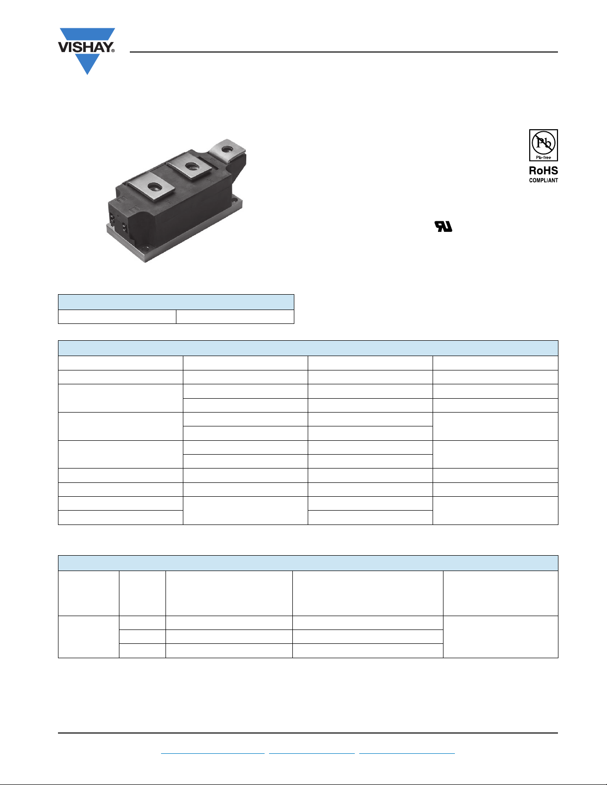
Thyristor/Diode and Thyristor/Thyristor
SUPER MAGN-A-PAK
(SUPER MAGN-A-PAK Power Modules), 430 A
PRODUCT SUMMARY
I
T(AV)
430 A
VSK.430..PbF Series
Vishay Semiconductors
FEATURES
• High current capability
• High surge capability
• High voltage ratings up to 2000 V
• 3000 V
substrate
• Industrial standard package
• UL approved file E78996
• Compliant to RoHS directive 2002/95/EC
TYPICAL APPLICATIONS
• Motor starters
• DC motor controls - AC motor controls
• Uninterruptable power supplies
• Wind mill
isolating voltage with non-toxic
RMS
MAJOR RATINGS AND CHARACTERISTICS
SYMBOL CHARACTERISTICS VALUES UNITS
I
T(AV)
I
T(RMS)
I
TSM
2
I
t
2
I
t 12 320 kA2s
V
RRM
T
J
T
Stg
82 °C 430 A
675 A
T
C
50 Hz 15.7
60 Hz 16.4
50 Hz 1232
60 Hz 1125
Range 1600 to 2000 V
Range
82 °C
- 40 to 150
- 40 to 130
ELECTRICAL SPECIFICATIONS
VOLTAGE RATINGS
TYPE
NUMBER
VSK.430..
V
RRM/VDRM
VOLTAGE
CODE
16 1600 1700
20 2000 2100
REPETITIVE PEAK
REVERSE VOLTAGE
, MAXIMUM
V
V
, MAXIMUM NON-REPETITIVE
RSM
PEAK REVERSE VOLTAGE
V
I
RRM/IDRM
= TJ MAXIMUM
AT T
J
kA
kA2s
°C
MAXIMUM
mA
10018 1800 1900
Document Number: 93748 For technical questions within your region, please contact one of the following: www.vishay.com
Revision: 02-Jul-10 DiodesAmericas@vishay.com
, DiodesAsia@vishay.com, DiodesEurope@vishay.com 1
VSK.430..PbF Series
Vishay Semiconductors
Thyristor/Diode and Thyristor/Thyristor
(SUPER MAGN-A-PAK Power Modules), 430 A
ON-STATE CONDUCTION
PARAMETER SYMBOL TEST CONDITIONS VALUES UNITS
Maximum average on-state current
I
at case temperature
Maximum RMS on-state current I
T(RMS)
Maximum peak, one-cycle,
non-repetitive surge current
Maximum I
Maximum I
2
t for fusing I2t
2
t for fusing I2t t = 0.1 ms to 10 ms, no voltage reapplied 12 320 kA2s
Low level value of threshold voltage V
High level value of threshold voltage V
Low level value of on-state slope resistance r
High level value of on-state slope
resistance
Maximum on-state voltage drop V
Maximum forward voltage drop V
Maximum holding current I
Typical latching current I
T(AV),
I
F(AV)
180° conduction, half sine wave
180° conduction, half sine wave at TC = 82 °C 675 A
t = 10 ms
I
TSM,
I
FSM
t = 8.3 ms 16.4
t = 10 ms
t = 8.3 ms 13.8
t = 10 ms
t = 8.3 ms 1125
t = 10 ms
t = 8.3 ms 795
F(TO)1
F(TO)2
r
(16.7 % x x I
(I > x I
(16.7 % x x I
f1
(I > x I
f2
Ipk = 1500 A, TJ = 25 °C, tp = 10 ms sine pulse 1.65 V
TM
Ipk = 1500 A, TJ = 25 °C, tp = 10 ms sine pulse 1.65 V
FM
H
TJ = 25 °C, anode supply 12 V resistive load
L
No voltage
reapplied
100 % V
reapplied
No voltage
RRM
Sinusoidal half wave,
initial T
= TJ maximum
J
reapplied
100 % V
RRM
reapplied
< I < x I
T(AV)
), TJ = TJ maximum 1.06
T(AV)
< I < x I
T(AV)
), TJ = TJ maximum 0.45
T(AV)
), TJ = TJ maximum 0.96
T(AV)
), TJ = TJ maximum 0.51
T(AV)
430 A
82 °C
15.7
13.2
1232
871
500
1000
kA
m
mA
kA
2
s
V
SWITCHING
PARAMETER SYMBOL TEST CONDITIONS VALUES UNITS
Maximum rate of rise of turned-on current dI/dt T
Typical delay time t
Typical turn-off time t
d
q
= TJ maximum, ITM = 400 A, V
J
Gate current 1 A, dIg/dt = 1 A/μs
V
= 0.67 % V
d
, TJ = 25 °C
DRM
ITM = 750 A, TJ = TJ maximum, dI/dt = - 60 A/μs
= 50, dV/dt = 20 V/μs, Gate 0 V 100
V
R
applied 1000 A/μs
DRM
2.0
200
μs
BLOCKING
PARAMETER SYMBOL TEST CONDITIONS VALUES UNITS
Maximum critical rate of rise of
off-state voltage
RMS insulation voltage V
Maximum peak reverse and
off-state leakage current
www.vishay.com For technical questions within your region, please contact one of the following: Document Number: 93748
2 DiodesAmericas@vishay.com
dV/dt T
INS
,
I
RRM
I
DRM
= 130 °C, linear to VD = 80 % V
J
DRM
1000 V/μs
t = 1 s 3000 V
TJ = TJ maximum, rated V
DRM/VRRM
applied 100 mA
, DiodesAsia@vishay.com, DiodesEurope@vishay.com Revision: 02-Jul-10
VSK.430..PbF Series
Thyristor/Diode and Thyristor/Thyristor
Vishay Semiconductors
(SUPER MAGN-A-PAK Power Modules), 430 A
THERMAL AND MECHANICAL SPECIFICATIONS
PARAMETER SYMBOL TEST CONDITIONS VALUES UNITS
Maximum junction operating
temperature range
Maximum storage temperature range T
Maximum thermal resistance,
junction to case per junction
Maximum thermal resistance,
case to heatsink
Mounting torque ± 10 %
Approximate weight 1500 g
Case style See dimensions - link at the end of datasheet SUPER MAGN-A-PAK
R
CONDUCTION ANGLE SINUSOIDAL CONDUCTION RECTANGULAR CONDUCTION TEST CONDITIONS UNITS
Note
• The table above shows the increment of thermal resistance R
CONDUCTION
thJC
180° 0.009 0.006
120° 0.011 0.011
90° 0.014 0.015
60° 0.021 0.022
30° 0.037 0.038
SMAP to heatsink
busbar to SMAP 12 to 15
R
R
T
J
Stg
thJC
thC-hs
DC operation 0.065
A mounting compound is recommended and
the torque should be rechecked after a period of
3 hours to allow for the spread of the compound.
= TJ maximum K/W
T
J
when devices operate at different conduction angles than DC
thJC
- 40 to 130
- 40 to 150
0.02
6 to 8
°C
K/W
Nm
Document Number: 93748 For technical questions within your region, please contact one of the following: www.vishay.com
Revision: 02-Jul-10 DiodesAmericas@vishay.com
, DiodesAsia@vishay.com, DiodesEurope@vishay.com 3
VSK.430..PbF Series
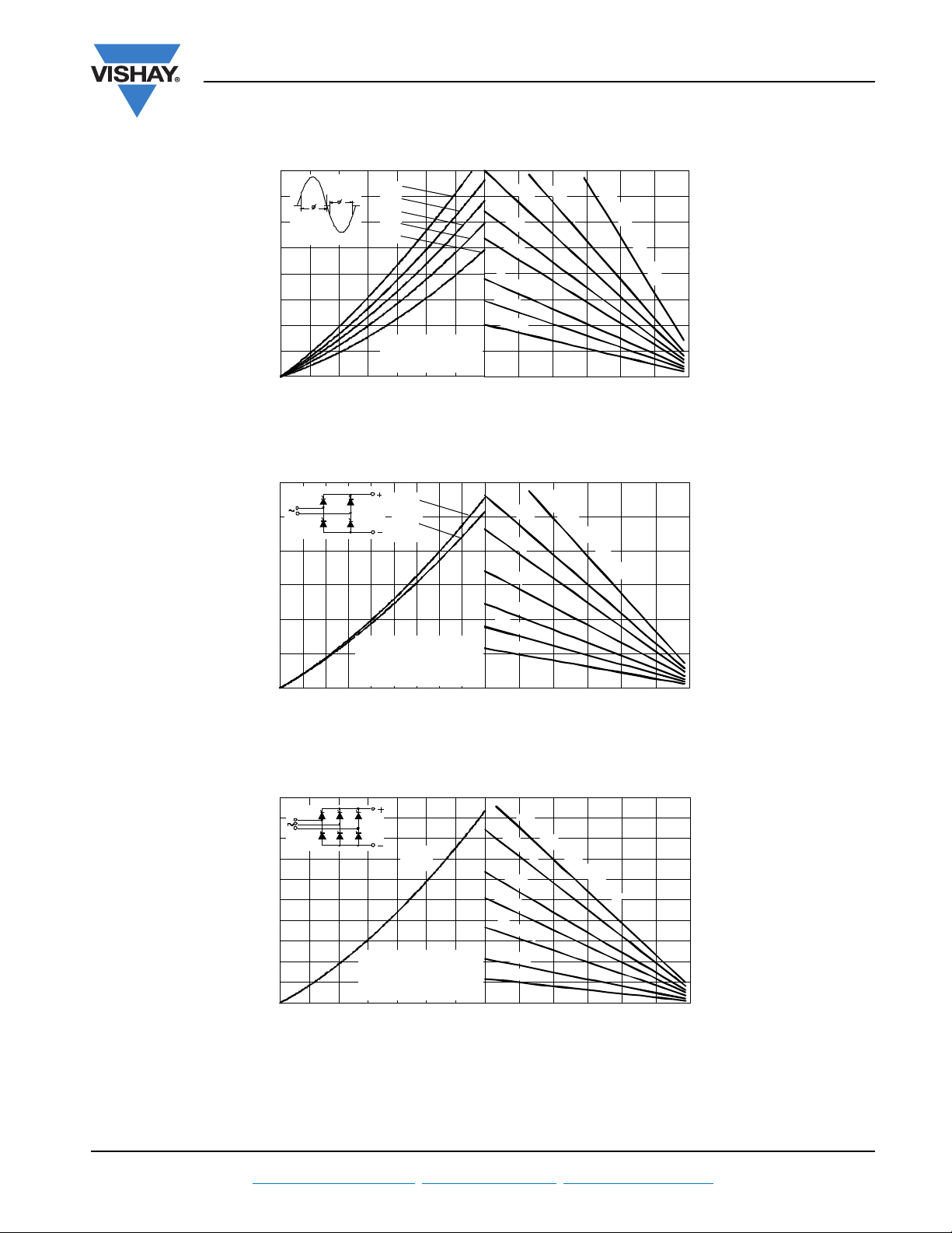
70
80
90
100
110
120
130
010020030040050
30°
60°
90°
120°
180°
Average On-state Current (A)
Maximum Allowable Case Temperature (°C)
Cond uc tio n An gle
VSK .430 ..PbF Se ries
R (DC) = 0.065 K/W
th JC
70
80
90
100
110
120
130
010020030040050060070
0
DC
30°
60°
90°
120°
180°
Average On-state Current (A)
Maximum Allowable Case Temperature (
°C
)
Conduction Period
VSK.430..PbF Series
R (DC ) = 0.065 K/W
thJC
0
100
200
300
400
500
600
700
01002003004005
00
RMS Limit
Conduction Angle
180°
120°
90°
60°
30°
Maximum Average On-state Power Loss (W)
Average On-state Current (A)
VSK .430..PbF Series
Per Junction
T = 130°C
J
6000
7000
8000
9000
10000
11000
12000
13000
14000
15000
16000
0.01 0.1
1
Peak Half Sine Wave On-state Current (A)
Pulse Train Duration (s)
Maximum Non Repetitive Surge Cu rren t
Versus Pul se T rain Duration. Control
Of Conduc tion May Not Be Maintained .
Initial T = 130° C
No Voltage Reapplied
Rated V Reapplied
RRM
J
VSK .430..PbF Series
Per Junction
Vishay Semiconductors
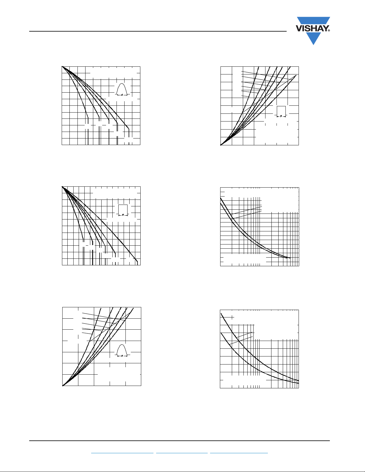
Fig. 1 - Current Ratings Characteristics
Fig. 2 - Current Ratings Characteristics
Thyristor/Diode and Thyristor/Thyristor
(SUPER MAGN-A-PAK Power Modules), 430 A
1000
900
800
700
600
500
400
300
200
100
0
Maximum Average On-state Power Loss (W)
Fig. 4 - On-State Power Loss Characteristics
15000
14000
13000
12000
11000
10000
9000
8000
7000
Peak Half Sine Wave On-state Current (A)
6000
Number Of Equa l Amplitude H alf Cycle C urrent Pulses (N)
Fig. 5 - Maximum Non-Repetitive Surge Current
DC
180°
120°
90°
60°
30°
RMS Limit
VSK.430..PbF Series
Per Juncti on
T = 130°C
J
0 100 20 0 300 400 500 600 70
Average O n-state Current (A)
At Any Rated Load Condition And With
Rat e d V A p plied F ol l ow in g Sur ge .
RRM
VSK.430..PbF Series
Per Junction
11010
Conduction Period
In it ial T = 130 °C
J
@ 6 0 Hz 0.0083 s
@ 5 0 Hz 0.0100 s
0
0
www.vishay.com For technical questions within your region, please contact one of the following: Document Number: 93748
4 DiodesAmericas@vishay.com
Fig. 3 - On-State Power Loss Characteristics
Fig. 6 - Maximum Non-Repetitive Surge Current
, DiodesAsia@vishay.com, DiodesEurope@vishay.com Revision: 02-Jul-10
0 20406080100120
Max imum Al lowable Am bient Te mpe ratu re ( °C
)
R
=
0
.
0
5
K
/
W
D
e
l
t
a
R
t
h
S
A
0
.
0
9
K
/
W
0
.
1
2
K
/
W
0
.
1
6
K
/
W
0
.
2
K
/
W
0
.
3
K
/
W
0
.
4
K
/
W
0
.
6
K/
W
0
100
200
300
400
500
600
700
800
0 100 200 300 400 500 600 700
180°
120°
90°
60°
30°
Total RMS Output Current (A)
Maximum Total On-state Power Loss (W
)
Conduct ion Angle
VSK .43 0. .PbF Serie s
Per M o dul e
T = 130°C
J
020406080100120
Maxi mum Allowab le Ambient Temperature (°C )
R
=
1
K
/
W
D
e
l
t
a
R
t
h
S
A
1
.
5
K
/
W
2
K
/
W
3
K
/
W
5
K
/
W
10
K/
W
1
5
K
/
W
0
500
1000
1500
2000
2500
3000
0 100 200 300 400 500 600 700 800 900
Tot al Ou tput Cur ren t ( A)
Maximum Total Power Loss (W)
180°
(Sine)
180°
(Rect )
2 x VSK.430..PbF Series
Single Phase Bridge
Connected
T = 130
°C
J
VSK.430..PbF Series
Thyristor/Diode and Thyristor/Thyristor
(SUPER MAGN-A-PAK Power Modules), 430 A
Fig. 7 - On-State Power Loss Characteristics
Vishay Semiconductors
Document Number: 93748 For technical questions within your region, please contact one of the following: www.vishay.com
Revision: 02-Jul-10 DiodesAmericas@vishay.com
Fig. 8 - On-State Power Loss Characteristics
5000
4500
4000
3500
3000
2500
2000
1500
1000
Maximum Total Power Loss (W)
500
0
0 200 400 600 800 1000 1200 1400
3 x VSK.430..PbF Series
Three Phase Bridge
Total Output Current (A)
Fig. 9 - On-State Power Loss Characteristics
R
t
h
S
A
0
=
.
0
0
1
.
0
K
0
120°
(Rect)
Conn ected
T = 130°C
J
/
5
W
K
/
0
.
0
2
K
/
W
0
.
0
3
K
/
W
0
.
0
5
K
/
W
0
.
1
K
/
W
0
2
.
K
/
W
W
D
e
l
t
a
R
0 20406080100120
Maximum Al lowable Ambient Temperature ( °C)
, DiodesAsia@vishay.com, DiodesEurope@vishay.com 5

VSK.430..PbF Series
100
1000
10000
0.511.522.533
.5
T = 25 °C
J
Instantaneous On-state Current (A)
In stan tan eo us O n -sta te Vo ltage ( V)
T = 130°C
J
VSK.430..PbF Series
Per Junctio n
Device code
1 - Module type
2 - Circuit configuration (see end of datasheet)
3
- Current rating
4 - Voltage code x 100 = V
RRM
(see Voltage Ratings table)
5 - Lead (Pb)-free
4132 5
VSK T 430 - 20 PbF
Vishay Semiconductors
Fig. 10 - On-State Voltage Drop Characteristics Fig. 11 - Thermal Impedance Z
100
Rectangular gate pulse
a) Recommended load line for
rated di/dt : 20V, 10ohms; tr< =1 µ s
b) Recommended load line for
<=30% rated di/dt : 10V, 10ohms
10
tr<=1 µs
1
Instantaneous Gate Voltage (V)
0.1
0.001 0. 01 0.1 1 10 10
Thyristor/Diode and Thyristor/Thyristor
(SUPER MAGN-A-PAK Power Modules), 430 A
0.1
VSK.430 ..PbF S er ies
Per Junct ion
thJC
0.01
Ste ady S tat e Value:
R = 0.065 K/W
thJC
(DC Operation)
(4)
0
VGD
(b)
Tj=25 °C
Tj=130
°C
IGD
VSK.430..PbF Series Fre quency L imi ted by PG( AV)
Instantaneous Ga te Current (A)
Fig. 12 - Gate Characteristics
Tr ansi ent The rma l I mpedan ce Z (K/W)
0.001
0.001 0.01 0.1 1 10 10
Square Wave Pulse Duration (s)
(1) PGM = 10W, tp = 4ms
(2) PGM = 20W, tp = 2ms
(3) PGM = 40W, tp = 1ms
(4) PGM = 60W, tp = 0.66ms
(a)
Tj=-40 °C
(2) (3)
(1)
Characteristics
thJC
0
ORDERING INFORMATION TABLE
Note
• To order the optional hardware go to www.vishay.com/doc?95172
www.vishay.com For technical questions within your region, please contact one of the following: Document Number: 93748
6 DiodesAmericas@vishay.com
, DiodesAsia@vishay.com, DiodesEurope@vishay.com Revision: 02-Jul-10
+
7
(K2)
6(G2)
-
4
(K1)
5(G1)
~
1
2
3
+
7(K2)
6(G2)
-
~
1
2
3
+
-
4(K1)
5(G1)
~
1
2
3
VSKT...
VSKH...
VSKL...
VSK.430..PbF Series
Thyristor/Diode and Thyristor/Thyristor
Vishay Semiconductors
(SUPER MAGN-A-PAK Power Modules), 430 A
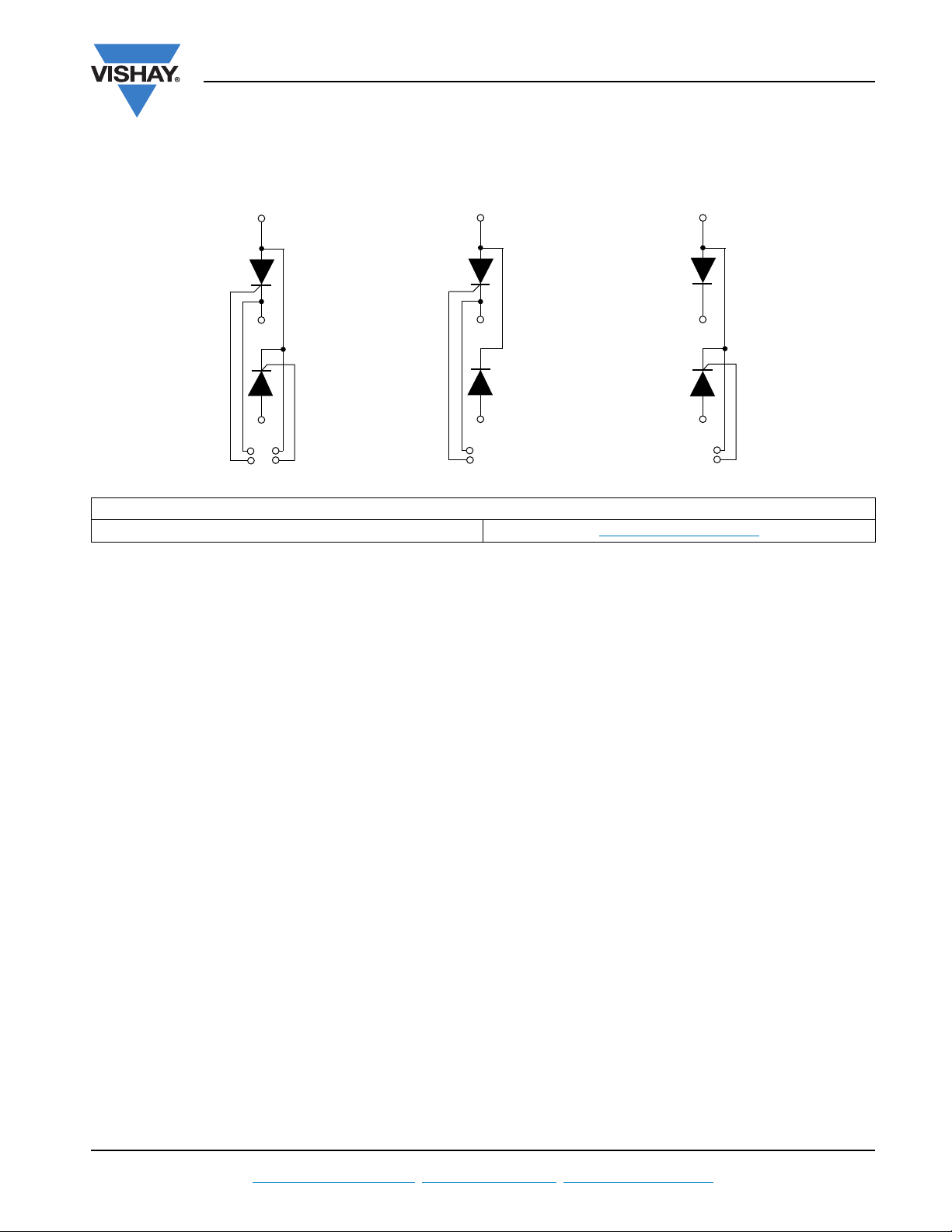
CIRCUIT CONFIGURATION
LINKS TO RELATED DOCUMENTS
Dimensions www.vishay.com/doc?95283
Document Number: 93748 For technical questions within your region, please contact one of the following: www.vishay.com
Revision: 02-Jul-10 DiodesAmericas@vishay.com
, DiodesAsia@vishay.com, DiodesEurope@vishay.com 7

Super MAGN-A-PAK Thyristor/Diode
52 (2.05)
60.0 (2.36)
48.0 (1.89)
31.0
(1.22)
50.0
(1.97)
44.0
(1.73)
M10
Fast-on tabs
2.8 x 0.8 (0.11 x 0.03)
20.1
(0.78)
36.4 (1.14) 4.5 (0.20)
54
6
5, 6 = Gate
4, 7 = Cathode
7
28.0
(1.10)
26.0
(0.98)
26.0
(0.98)
112.0 (4.41)
124.0 (4.88)
149.0 (5.67)
1.0 (0.039)
32
1
DIMENSIONS in millimeters (inches)
Outline Dimensions
Vishay Semiconductors
Document Number: 95283 For technical questions, contact: indmodules@vishay.com
Revision: 20-Mar-08 1
www.vishay.com

Legal Disclaimer Notice
Vishay
Disclaimer
ALL PRODUCT, PRODUCT SPECIFICATIONS AND DATA ARE SUBJECT TO CHANGE WITHOUT NOTICE TO IMPROVE
RELIABILITY, FUNCTION OR DESIGN OR OTHERWISE.
Vishay Intertechnology, Inc., its affiliates, agents, and employees, and all persons acting on its or their behalf (collectively,
“Vishay”), disclaim any and all liability for any errors, inaccuracies or incompleteness contained in any datasheet or in any other
disclosure relating to any product.
Vishay makes no warranty, representation or guarantee regarding the suitability of the products for any particular purpose or
the continuing production of any product. To the maximum extent permitted by applicable law, Vishay disclaims (i) any and all
liability arising out of the application or use of any product, (ii) any and all liability, including without limitation special,
consequential or incidental damages, and (iii) any and all implied warranties, including warranties of fitness for particular
purpose, non-infringement and merchantability.
Statements regarding the suitability of products for certain types of applications are based on Vishay’s knowledge of typical
requirements that are often placed on Vishay products in generic applications. Such statements are not binding statements
about the suitability of products for a particular application. It is the customer’s responsibility to validate that a particular
product with the properties described in the product specification is suitable for use in a particular application. Parameters
provided in datasheets and/or specifications may vary in different applications and performance may vary over time. All
operating parameters, including typical parameters, must be validated for each customer application by the customer’s
technical experts. Product specifications do not expand or otherwise modify Vishay’s terms and conditions of purchase,
including but not limited to the warranty expressed therein.
Except as expressly indicated in writing, Vishay products are not designed for use in medical, life-saving, or life-sustaining
applications or for any other application in which the failure of the Vishay product could result in personal injury or death.
Customers using or selling Vishay products not expressly indicated for use in such applications do so at their own risk and agree
to fully indemnify and hold Vishay and its distributors harmless from and against any and all claims, liabilities, expenses and
damages arising or resulting in connection with such use or sale, including attorneys fees, even if such claim alleges that Vishay
or its distributor was negligent regarding the design or manufacture of the part. Please contact authorized Vishay personnel to
obtain written terms and conditions regarding products designed for such applications.
No license, express or implied, by estoppel or otherwise, to any intellectual property rights is granted by this document or by
any conduct of Vishay. Product names and markings noted herein may be trademarks of their respective owners.
Document Number: 91000 www.vishay.com
Revision: 11-Mar-11 1
 Loading...