

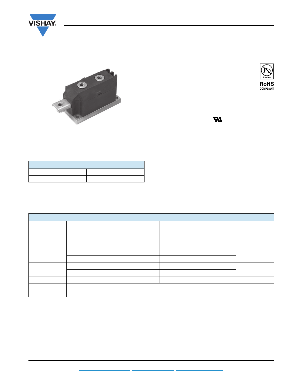
Standard Recovery Diodes, 250 A to 320 A
MAGN-A-PAK
PRODUCT SUMMARY
I
F(AV)
Type Modules - Diode, High Voltage
VSK.250, VSK.270, VSK.320 Series
Vishay Semiconductors
(MAGN-A-PAK Power Modules)
FEATURES
• High voltage
• Electrically isolated base plate
250 A to 320 A
• 3000 V
• Industrial standard package
• Simplified mechanical designs, rapid assembly
• High surge capability
• Large creepage distances
• UL approved file E78996
• Compliant to RoHS directive 2002/95/EC
• Designed and qualified for industrial level
DESCRIPTION
This new VSK series of MAGN-A-PAKs uses high voltage
power diodes in two basic configurations. The
semiconductors are electrically isolated from the metal
base, allowing common heatsinks and compact assemblies
to be built. They can be interconnected to form single phase
or three phase bridges and the single diode module can be
used in conjunction with the thyristor modules as a
freewheel diode. These modules are intended for general
purpose applications such as battery chargers, welders and
plating equipment and where high voltage and high current
are required (motor drives, etc.).
isolating voltage
RMS
MAJOR RATINGS AND CHARACTERISTICS
SYMBOL CHARACTERISTICS VSK.250.. VSK.270.. VSK.320.. UNITS
I
F(AV)
I
F(RMS)
I
FSM
2
t
I
2
I
t 2460 3980 5110 kA2s
V
RRM
T
J
Document Number: 93581 For technical questions within your region, please contact one of the following: www.vishay.com
Revision: 02-Jul-10 DiodesAmericas@vishay.com
T
C
50 Hz 7015 8920 10 110
60 Hz 7345 9430 10 580
50 Hz 246 398 511
60 Hz 225 363 466
250 270 320 A
100 100 100 °C
393 424 502
A
kA2s
400 to 3000 V
- 40 to 150 °C
, DiodesAsia@vishay.com, DiodesEurope@vishay.com 1
VSK.250, VSK.270, VSK.320 Series
Vishay Semiconductors
Standard Recovery Diodes, 250 A to 320 A
(MAGN-A-PAK Power Modules)
ELECTRICAL SPECIFICATIONS
VOLTAGE RATINGS
V
MAXIMUM REPETITIVE
TYPE NUMBER
VOLTAGE
CODE
RRM,
PEAK REVERSE VOLTAGE
V
04 400 500
VSK.250
VSK.270
VSK.320
08 800 900
12 1200 1300
16 1600 1700
20 2000 2100
VSK.270 30 3000 3100
FORWARD CONDUCTION
PARAMETER SYMBOL TEST CONDITIONS VSK.250 VSK.270 VSK.320 UNITS
Maximum average forward
current at case temperature
Maximum RMS forward current I
Maximum peak, one-cycle
forward, non-repetitive
surge current
2
Maximum I
Maximum I
Low level value of
threshold voltage
High level value of
threshold voltage
t for fusing I2t
2
t for fusing I2t t = 0.1 ms to 10 ms, no voltage reapplied 2460 3980 5110 kA2s
V
V
Low level forward
slope resistance
High level forward
slope resistance
Maximum forward voltage drop V
I
F(AV)
F(RMS)
I
FSM
F(TO)1
F(TO)2
r
f1
r
f2
FM
180° conduction, half sine wave
As AC switch 393 424 502
t = 10 ms
t = 8.3 ms 7345 9340 10 580
t = 10 ms
t = 8.3 ms 6180 7850 8900
t = 10 ms
t = 8.3 ms 225 363 466
t = 10 ms
t = 8.3 ms 159 257 330
(16.7 % x x I
T
= TJ maximum
J
(I > x I
(16.7 % x x I
T
= TJ maximum
J
(I > x I
IFM = x I
Average power = V
No voltage
reapplied
100 % V
RRM
reapplied
No voltage
reapplied
100 % V
RRM
reapplied
< I < x I
F(AV)
), TJ = TJ maximum 0.92 0.87 0.86
F(AV)
< I < x I
F(AV)
), TJ = TJ maximum 0.49 0.81 0.44
F(AV)
, TJ = TJ maximum, 180° conduction
F(AV)
F(TO)
x I
V
, MAXIMUM NON-REPETITIVE
RSM
PEAK REVERSE VOLTAGE
Sinusoidal half wave,
initial T
= T
J
J m
),
F(AV)
),
F(AV)
+ rf x (I
F(AV)
F(RMS)
aximum
2
)
I
RRM
V
250 270 320 A
100 100 100 °C
7015 8920 10 110
5900 7500 8500
246 398 511
174 281 361
0.79 0.74 0.69
0.63 0.94 0.59
1.29 1.48 1.28 V
MAXIMUM
AT 150 °C
mA
50
A
kA2s
V
m
BLOCKING
PARAMETER SYMBOL TEST CONDITIONS VALUES UNITS
Maximum peak reverse
leakage current
RMS insulation voltage V
www.vishay.com For technical questions within your region, please contact one of the following: Document Number: 93581
2 DiodesAmericas@vishay.com
I
RRM
INS
TJ = 150 °C 50 mA
50 Hz, circuit to base, all terminals shorted, t = 1 s 3000 V
, DiodesAsia@vishay.com, DiodesEurope@vishay.com Revision: 02-Jul-10
VSK.250, VSK.270, VSK.320 Series
Standard Recovery Diodes, 250 A to 320 A
Vishay Semiconductors
(MAGN-A-PAK Power Modules)
THERMAL AND MECHANICAL SPECIFICATIONS
PARAMETER SYMBOL TEST CONDITIONS
Maximum junction operating and storage
temperature range
Maximum thermal resistance,
junction to case per junction
Maximum resistance, case to heatsink
per module
Mounting torque
± 10 %
Approximate weight
Case style MAGN-A-PAK
MAP to heatsink
busbar to MAP 8 to 10
T
, T
J
Stg
DC operation 0.16 0.125
Mounting surface flat, smooth and
greased
A mounting compound is recommended
and the torque should be rechecked
after a period of about 3 hours to allow for
the spread of the compound.
R
R
thJC
thCS
VSK.250 VSK.270 VSK.320
R CONDUCTION PER JUNCTION
SINUSOIDAL CONDUCTION
AT T
MAXIMUM
DEVICE
180° 120° 90° 60° 30° 180° 120° 90° 60° 30°
VSK.250 0.009 0.010 0.014 0.020 0.032 0.007 0.011 0.015 0.021 0.033
VSK.320 0.008 0.010 0.013 0.020 0.032 0.007 0.011 0.015 0.020 0.033
Note
• The table above shows the increment of thermal resistance R
J
when devices operate at different conduction angles than DC
thJC
RECTANGULAR CONDUCTION
AT TJ MAXIMUM
VALUES
- 40 to 150 °C
0.035
4 to 6
800 g
30 oz.
UNITS
K/W
Nm
UNITS
K/WVSK.270 0.008 0.012 0.014 0.020 0.032 0.007 0.011 0.015 0.020 0.033
Document Number: 93581 For technical questions within your region, please contact one of the following: www.vishay.com
Revision: 02-Jul-10 DiodesAmericas@vishay.com
, DiodesAsia@vishay.com, DiodesEurope@vishay.com 3

VSK.250, VSK.270, VSK.320 Series
80
90
100
110
120
130
140
150
0 50 100 150 200 250 300
30°
60°
90°
120°
180°
Maximum Allowable Case Temperature (°C)
Conduction Angle
Average Forward Current (A)
VSK.250 .. Seri e s
R (DC) = 0.16 K/ W
thJC
80
90
100
110
120
130
140
150
0 50 100 150 200 250 300 350 400
DC
30°
60°
90°
120°
180°
Maximu m Allow able C ase Tem perature (°C)
Conduction Period
Average Forward Current (A)
VSK.250 .. Se ri e s
R (DC) = 0.16 K/ W
thJC
0
50
100
150
200
250
300
0 50 100 150 200 250
Ave rag e Forw ard Cu rre nt (A )
RM S Lim it
Maximum Ave rag e Fo rward Power Loss (W)
Cond uct ion Ang le
180°
120°
90°
60°
30°
VSK.250.. Serie s
T = 15 0° C
J
0 25 50 75 100 125 150
Maximum Allowable Ambient Temperature (°C)
R
=
0
.
0
2
K
/
W
D
e
l
t
a
R
t
h
S
A
0
.
0
8
K
/
W
0
.
2
K
/
W
0
.
2
5
K
/
W
0
.
4
K
/
W
0
.
1
2
K
/
W
0
.
6
K
/
W
0
100
200
300
400
500
600
0 50 100 150 200 250 3 00 350 400
Total RMS Output Current (A)
Maximum Tota l Forward Po wer Loss (W)
180°
(Sine)
DC
VSK.25 0.. Seri e s
Pe r Ju nc t io n
T = 15 0° C
J
Vishay Semiconductors
Fig. 1 - Current Ratings Characteristics
Fig. 2 - Current Ratings Characteristics
Standard Recovery Diodes, 250 A to 320 A
(MAGN-A-PAK Power Modules)
Fig. 3 - Forward Power Loss Characteristics
450
400
350
300
250
200
150
100
50
0
Maximum Average Forward Power Loss (W)
Fig. 4 - Forward Power Loss Characteristics
DC
180°
120°
90°
60°
30°
RM S Li m i t
0 50 10 0 150 200 250 300 350 400
Average Forward Current (A)
Conduction Period
VSK.250.. Series
T = 150°C
J
www.vishay.com For technical questions within your region, please contact one of the following: Document Number: 93581
4 DiodesAmericas@vishay.com
Fig. 5 - Forward Power Loss Characteristics
, DiodesAsia@vishay.com, DiodesEurope@vishay.com Revision: 02-Jul-10

0 255075100125150
Maximum Allowa ble Ambient Temperature (°C)
0
.
0
8
K
/
W
0
.
1
K
/
W
0
.
1
6
K
/
W
0
.
2
5
K
/
W
0
.
0
3
K
/
W
0
.
0
5
K
/
W
0
.
3
5
K
/
W
R
=
0
.
0
1
K
/
W
D
e
l
t
a
R
t
h
S
A
0
200
400
600
800
1000
1200
0 100 200 300 400 500
Total Output Current (A)
Ma ximu m To tal Powe r Loss (W)
180°
(Sine)
180°
(Re c t)
2 x VSK.250.. Serie s
Single Phase Bridge
Connec ted
T = 1 5 0 ° C
J
0 255075100125150
Maximum Allowable Ambient Temperature (°C)
0
.
2
5
K
/
W
R
=
0
.
0
0
5
K
/
W
-
D
e
l
t
a
R
t
h
S
A
0
.
0
2
K
/
W
0
.
0
4
K
/
W
0
.
0
6
K
/
W
0
.
0
8
K
/
W
0
.
1
2
K
/
W
0
.
1
6
K
/
W
0
.
3
5
K
/
W
0
200
400
600
800
1000
1200
1400
1600
1800
0 100200300400500600700800
Total Output Current (A)
Maximum Total Power Loss (W)
120°
(Rec t)
3 x VSK.250.. Se ries
Three Phase Bridge
Connec ted
T = 1 50 ° C
J
1500
2000
2500
3000
3500
4000
4500
5000
5500
6000
6500
110100
Peak Half Sine Wave Forward Current (A)
Nu mb e r O f Eq u a l Am pli tu d e Ha lf C yc le Cu rre nt Pul se s (N)
Initia l T = 150°C
@ 60 Hz 0.0083 s
@ 50 Hz 0.0100 s
J
VSK.250.. Serie s
Pe r Ju nc t io n
At Any Rated Load Cond itio n And With
Rated V Applied Following Surge.
RRM
VSK.250, VSK.270, VSK.320 Series
Standard Recovery Diodes, 250 A to 320 A
(MAGN-A-PAK Power Modules)
Fig. 6 - Forward Power Loss Characteristics
Vishay Semiconductors
Document Number: 93581 For technical questions within your region, please contact one of the following: www.vishay.com
Revision: 02-Jul-10 DiodesAmericas@vishay.com
Fig. 8 - Maximum Non-Repetitive Surge Current Fig. 9 - Maximum Non-Repetitive Surge Current
Fig. 7 - Forward Power Loss Characteristics
7000
Maximum Non Repetitive Surge Current
6500
6000
5500
5000
4500
4000
3500
3000
2500
2000
Peak Half Sine Wave Forward Current (A)
, DiodesAsia@vishay.com, DiodesEurope@vishay.com 5
1500
0.01 0.1 1
Versus Pulse Train Duration.
No Volt a g e Rea pp lied
Ra t e d V Re a p p l i e d
VSK.250 .. Seri e s
Pe r J u nc t io n
Pu lse Tr ai n Dura t io n ( s)
Init ia l T = 150°C
J
RRM

VSK.250, VSK.270, VSK.320 Series
0.001
0.01
0.1
1
0.001 0.01 0.1 1 10 100
Sq ua re Wave Pulse Durat ion (s)
thJC
VSK.250.. Seri es
Pe r J u n ct i o n
Steady Sta te Value:
R = 0. 16 K/ W
(DC Operation)
thJC
Transient Thermal Impedance Z (K/W)
80
90
100
110
120
130
140
150
0 50 100 150 200 250 300
30°
60°
90°
120°
180°
Maximum Allo wable Case Temperature (°C)
Conduction Angle
Average Forward Current (A)
VSK.270 .. Se ri e s
R (DC) = 0.125 K/ W
thJC
0
50
100
150
200
250
300
350
400
450
500
0 50 100 1 50 2 00 250 300 35 0 400 450
DC
180°
120°
90°
60°
30°
Average Forward Current (A)
RM S Li m i t
Maximum Average Forward Power Loss (W)
Co nduct ion Period
VSK.270.. Seri e s
T = 1 50 ° C
J
Vishay Semiconductors
10000
T = 2 5 ° C
J
1000
100
VSK.250.. Se rie s
Instantaneous Forward Current (A)
10
0.5 1 1.5 2 2.5 3 3.5 4
Instantaneous Forward Voltage (V)
Fig. 10 - Forward Voltage Drop Characteristics
Fig. 11 - Thermal Impedance Z
Pe r Ju n c t io n
Standard Recovery Diodes, 250 A to 320 A
(MAGN-A-PAK Power Modules)
150
140
T = 1 5 0 °C
J
Characteristics
thJC
130
120
110
100
90
80
Maximum Allowab le Case Temperature (°C)
0 100 200 300 400 500
Average Forward Current (A)
Fig. 13 - Current Ratings Characteristics
400
350
180°
120°
300
250
200
150
100
Maximum Average Forward Power Loss (W)
90°
60°
30°
50
0
0 50 100 150 200 250 300
Average Forward Current (A)
Fig. 14 - Forward Power Loss Characteristics
VSK.270.. Serie s
R (DC ) = 0.125 K/ W
thJC
30°
60°
90°
120°
Conduction Period
180°
DC
RM S Li m it
Conduction Angle
VSK.270.. Se rie s
T = 1 50 ° C
J
Fig. 12 - Current Ratings Characteristics
www.vishay.com For technical questions within your region, please contact one of the following: Document Number: 93581
6 DiodesAmericas@vishay.com
Fig. 15 - Forward Power Loss Characteristics
, DiodesAsia@vishay.com, DiodesEurope@vishay.com Revision: 02-Jul-10

0 255075100125150
0
.
0
6
K
/
W
0
.
1
K
/
W
0
.
1
6
K
/
W
0
.
2
5
K
/
W
0
.
4
K
/
W
0
.
6
K
/
W
Maximum Allowable Ambient Temperature (°C)
R
=
0
.
0
2
K
/
W
D
e
l
t
a
R
0
.
0
4
K
/
W
t
h
S
A
0
300
600
900
1200
1500
1800
2100
2400
0200400600800
120°
(Rect )
Maximum Tota l Po wer Loss (W)
Total Output Current (A)
3 x VSK.270.. Serie s
Three Phase Bridge
Connected
T = 150° C
J
VSK.250, VSK.270, VSK.320 Series
Standard Recovery Diodes, 250 A to 320 A
(MAGN-A-PAK Power Modules)
700
600
500
180°
400
(Sine)
300
200
VSK.270. . Se rie s
100
Maximum Total Forward Power Lo ss (W)
0
0 50 100 150 200 250 300 350 400
Pe r Ju n c ti o n
T = 15 0° C
To t a l RM S O u t p u t C u r r e n t ( A )
Fig. 16 - Forward Power Loss Characteristics
1800
1600
1400
1200
1000
800
180°
(Sine)
180°
(Rec t)
600
400
Maximum Total Power Loss (W)
200
0
0 100 200 300 400 500 600
2 x VSK.270. . Se rie s
Sin gle Pha se Bridge
Connected
T = 1 50 ° C
J
Total Output Curre nt (A)
Fig. 17 - Forward Power Loss Characteristics
DC
J
0 25 50 75 100 12 5 150
Maximum Allowable Ambient Temperature (°C)
0 255075100125150
Maximum Allowable Ambient Temperature (°C)
R
0
t
.
h
0
S
6
A
K
=
/
W
0
.
1
K
/
0
.
1
6
K
0
.
2
5
K
0
.
3
K
0
.
4
K
0
.
6
K
0
.
0
6
0
.
0
8
K
0
.
1
2
K
0
.
1
6
0
.
2
5
0
.
4
K
0
.
6
K
0
.
0
2
W
/
W
/
W
/
W
/
W
/
W
0
.
0
4
K
/
W
/
W
/
W
K
/
W
K
/
W
/
W
/
W
K
/
W
R
0
.
t
3
h
K
S
A
/
K
W
/
W
Vishay Semiconductors
D
e
l
t
a
R
=
0
.
0
2
K
/
W
D
e
l
t
a
R
Document Number: 93581 For technical questions within your region, please contact one of the following: www.vishay.com
Revision: 02-Jul-10 DiodesAmericas@vishay.com
Fig. 18 - Forward Power Loss Characteristics
, DiodesAsia@vishay.com, DiodesEurope@vishay.com 7

VSK.250, VSK.270, VSK.320 Series
2000
3000
4000
5000
6000
7000
8000
110100
Pea k Ha lf Sine Wave Forward Current (A)
Number Of Equal Amplitude Half Cyc le Current Pulses (N)
Initial T = 150°C
@ 60 Hz 0.0083 s
@ 50 Hz 0.0100 s
At Any Ra ted Load Condition And With
Rated V Applied Following Surge.
RRM
J
VSK.270.. Serie s
Pe r Ju nc t io n
10
100
1000
10000
0.511.522.533.54
T = 25 °C
J
Instantaneous Forward Current (A)
Instantaneous Forward Voltage (V)
T = 150° C
J
VSK.270 .. Ser ie s
Pe r Ju nc t io n
0.001
0.01
0.1
1
0.001 0.01 0.1 1 10 100
Sq ua re Wa ve Pulse Dura tio n (s)
thJC
Steady State Value:
R = 0.45 K/W
(DC Operation)
thJC
VSK.270. . Se rie s
Pe r Ju nc t io n
Tra nsien t Therma l Impe danc e Z (K/ W)
Vishay Semiconductors
Fig. 19 - Maximum Non-Repetitive Surge Current
9000
Ma ximum No n Repet itiv e Surge Current
8000
7000
6000
Versus Pulse Train Duration.
Init ia l T = 150°C
No Volta g e Rea pp lied
Ra t ed V Re a p p l i e d
RRM
Standard Recovery Diodes, 250 A to 320 A
(MAGN-A-PAK Power Modules)
Fig. 22 - Thermal Impedance Z
150
J
140
130
120
Characteristics
thJC
VSK.320.. Ser ie s
R ( D C ) = 0. 12 5 K / W
thJC
Conduction Angle
5000
4000
3000
VSK.270.. Se rie s
Pe a k Ha lf Sine Wave Forward Current (A)
Pe r Ju nc t io n
2000
0.01 0.1 1
Pu l se Tra in D u ra t io n ( s)
Fig. 20 - Maximum Non-Repetitive Surge Current
Fig. 21 - Forward Voltage Drop Characteristics
110
30°
100
90
80
Maximum Allowable Case Temperat ure (°C)
0 50 100 150 200 250 300 350
Average Forward Current (A)
60°
90°
120°
Fig. 23 - Current Ratings Characteristics
150
140
130
120
110
100
90
80
Maximum Allowable Case Tem perature (°C)
0 100 200 300 400 500 600
Av er a g e Fo rwa rd C urren t (A)
VSK.320.. Series
R ( DC ) = 0 .1 25 K/ W
thJC
30°
60°
90°
120°
Cond uc tion Period
180°
DC
Fig. 24 - Current Ratings Characteristics
180°
www.vishay.com For technical questions within your region, please contact one of the following: Document Number: 93581
8 DiodesAmericas@vishay.com
, DiodesAsia@vishay.com, DiodesEurope@vishay.com Revision: 02-Jul-10

0
50
100
150
200
250
300
350
400
0 5 0 100 1 50 2 00 250 3 00 350
Average Forward Current (A)
RM S Li m it
Maximum Average Forward Power Loss (W)
Conduction Angle
180°
120°
90°
60°
30°
VSK.320.. Se ries
T = 150°C
J
0 2 5 50 75 1 00 125 150
0
.
1
K
/
W
0
.
2
K
/
W
0
.
6
K
/
W
0
.
0
6
K
/
W
0
.
3
K
/
W
0
.
4
K
/
W
Maximum Allowable Ambient Temperature (°C)
R
=
0
.
0
2
K
/
W
D
e
l
t
a
R
0
.
1
6
K
/
W
0
.
0
4
K
/
W
t
h
S
A
0
100
200
300
400
500
600
700
0 100 200 300 400 500
DC
180°
(Sine)
Total RMS Output Current (A)
VSK.320.. Serie s
Pe r Ju n c ti on
T = 150°C
Maximum To tal Forward Power Loss (W)
J
VSK.250, VSK.270, VSK.320 Series
Standard Recovery Diodes, 250 A to 320 A
Vishay Semiconductors
(MAGN-A-PAK Power Modules)
500
DC
450
180°
120°
400
90°
60°
350
30°
300
250
RMS Lim it
200
150
100
50
0
Maximum Average Forward Powe r Loss (W)
0 1 00 200 300 400 500 600
Average Forward Current (A)
Fig. 25 - Forward Power Loss Characteristics Fig. 26 - Forward Power Loss Characteristics
Cond uct ion Period
VSK.320 .. Serie s
Pe r Ju nc t io n
T = 150°C
J
Document Number: 93581 For technical questions within your region, please contact one of the following: www.vishay.com
Revision: 02-Jul-10 DiodesAmericas@vishay.com
Fig. 27 - Forward Power Loss Characteristics
1400
0
1200
180°
1000
800
(Sine)
180°
(Re ct)
600
400
200
M a xi mu m To t a l P ow e r Lo ss ( W)
0
0 100 200 300 400 500 600
Total Output Current (A)
2 x VSK.320.. Se ries
Si n g l e Ph a se Br i d g e
Connec ted
T = 150° C
J
Fig. 28 - Forward Power Loss Characteristics
, DiodesAsia@vishay.com, DiodesEurope@vishay.com 9
.
0
8
K
/
0
.
1
2
K
/
0
.
1
6
K
/
0
.
2
5
K
/
0
.
5
K
/
W
0
.
6
K
/
W
0255075100125150
Maximum Allowable Ambient Temperature (°C)
0
0
0
.
0
6
K
/
W
W
W
W
W
R
.
.
0
0
t
3
4
h
S
K
K
A
/
/
W
=
W
0
.
0
2
K
/
W
D
e
l
t
a
R

VSK.250, VSK.270, VSK.320 Series
2000
3000
4000
5000
6000
7000
8000
9000
10000
0.01 0.1 1
Peak Half Sine Wave Forward Current (A)
Pulse Train Duration (s)
Maximum Non Rep etitive Surge Current
Ini t ia l T = 150°C
No Voltage Reapplied
Ra t ed V Re a p p l ie d
Versus Pulse Train Duration.
RRM
J
VSK.320.. Series
Pe r Ju nc t io n
0.001
0.01
0.1
1
0.001 0.01 0.1 1 10 100
Square Wave Pulse Duration (s)
thJC
Transient T
he rmal Imp ed a nc e Z (K/W)
VSK.320.. Se ries
Pe r Ju nc t io n
St e a d y St a t e V a l u e :
R = 0. 45 K/ W
(DC Operation)
thJC
Vishay Semiconductors
2800
2400
2000
1600
1200
800
400
M a xi m u m To t a l Po w e r L o ss ( W)
0
0 200 4 00 600 800 1000
10000
At Any Ra ted Lo ad Condition And With
Rat ed V App lied Following Surge .
9000
8000
7000
6000
5000
4000
3000
Peak Half Sine Wave Forward Current (A)
2000
110100
Number Of Equa l Amplitude Half Cycle Current Pulses (N)
Fig. 30 - Maximum Non-Repetitive Surge Current
RRM
VSK.320 .. Se ries
Pe r J u nc t io n
Initial T = 150°C
@ 60 Hz 0.0083 s
@ 50 Hz 0.0100 s
Standard Recovery Diodes, 250 A to 320 A
(MAGN-A-PAK Power Modules)
R
0.
t
h
0
3
S
A
K
=
/W
0
0
.
0
4
K
0
.
0
5
120°
(Re ct)
3 x VSK.320.. Serie s
Three Phase Bridge
Connec t ed
T = 15 0° C
J
K
0
.
0
6
K
0
.
0
8
K
0
.
1
2
0
.
2
K
0
.
3
K
0
.
6
K
0 25 50 75 100 125 150
Total Output Current (A)
Maximum Allowable Ambient Temperature (°C)
Fig. 29 - Forward Power Loss Characteristics
J
.
0
2
K
/
W
/
W
/
W
/
W
K
/
W
/
W
/
W
/
W
/
W
D
e
l
t
a
R
10000
T = 2 5 ° C
J
1000
Inst anta neous Forward Curre nt (A)
100
0.5 1 1.5 2 2.5 3 3.5 4
In st a n t a n eo u s Fo rw a rd Vo l t a g e ( V )
Fig. 32 - Forward Voltage Drop Characteristics
T = 1 5 0 ° C
J
VSK.320.. Se ries
Pe r Ju nc t io n
Fig. 31 - Maximum Non-Repetitive Surge Current
www.vishay.com For technical questions within your region, please contact one of the following: Document Number: 93581
10 DiodesAmericas@vishay.com
Fig. 33 - Thermal Impedance Z
Characteristics
thJC
, DiodesAsia@vishay.com, DiodesEurope@vishay.com Revision: 02-Jul-10

VSKC...
+
--
+
-
-
VSKJ...
-++
-
+
+
VSKE...
+-
+-
VSK.250, VSK.270, VSK.320 Series
Standard Recovery Diodes, 250 A to 320 A
(MAGN-A-PAK Power Modules)
ORDERING INFORMATION TABLE
Device code
CIRCUIT CONFIGURATION
CIRCUIT DESCRIPTION
Vishay Semiconductors
VSK D 320 - 24
1324
1 - Module type
2 - Circuit configuration (see Circuit Configuration table)
3
- Current rating: I
4 - Voltage code x 100 = V
CIRCUIT
CONFIGURATION CODE
F(AV)
rounded
(see Voltage Ratings table)
RRM
CIRCUIT DRAWING
~
VSKD...
+
-
Two diodes doubler circuit D
Two diodes common cathodes C
Two diodes common anodes J
Single diode E
-
~
+
Dimensions www.vishay.com/doc?95086
Document Number: 93581 For technical questions within your region, please contact one of the following: www.vishay.com
Revision: 02-Jul-10 DiodesAmericas@vishay.com
LINKS TO RELATED DOCUMENTS
, DiodesAsia@vishay.com, DiodesEurope@vishay.com 11

DIMENSIONS in millimeters (inches)
Outline Dimensions
Vishay Semiconductors
MAGN-A-PAK
3 screws M8 x 1.25
20 (0.79)
32
(1.26)
HEX 13
9 (0.35)
35 (1.38) 28 (1.12)
80 (3.15)
115 (4.53)
Ø 5.5
6
38 (1.5)
6 (0.24)
51 (2.01)
(0.24)
50 (1.97)
52 (2.04)
10 (0.39)
Notes
• Dimensions are nominal
• Full engineering drawings are available on request
• UL identification number for gate and cathode wire: UL 1385
• UL identification number for package: UL 94 V-0
Document Number: 95086 For technical questions, contact: indmodules@vishay.com
Revision: 03-Aug-07 1
92 (3.62)
www.vishay.com

Legal Disclaimer Notice
Vishay
Disclaimer
ALL PRODUCT, PRODUCT SPECIFICATIONS AND DATA ARE SUBJECT TO CHANGE WITHOUT NOTICE TO IMPROVE
RELIABILITY, FUNCTION OR DESIGN OR OTHERWISE.
Vishay Intertechnology, Inc., its affiliates, agents, and employees, and all persons acting on its or their behalf (collectively,
“Vishay”), disclaim any and all liability for any errors, inaccuracies or incompleteness contained in any datasheet or in any other
disclosure relating to any product.
Vishay makes no warranty, representation or guarantee regarding the suitability of the products for any particular purpose or
the continuing production of any product. To the maximum extent permitted by applicable law, Vishay disclaims (i) any and all
liability arising out of the application or use of any product, (ii) any and all liability, including without limitation special,
consequential or incidental damages, and (iii) any and all implied warranties, including warranties of fitness for particular
purpose, non-infringement and merchantability.
Statements regarding the suitability of products for certain types of applications are based on Vishay’s knowledge of typical
requirements that are often placed on Vishay products in generic applications. Such statements are not binding statements
about the suitability of products for a particular application. It is the customer’s responsibility to validate that a particular
product with the properties described in the product specification is suitable for use in a particular application. Parameters
provided in datasheets and/or specifications may vary in different applications and performance may vary over time. All
operating parameters, including typical parameters, must be validated for each customer application by the customer’s
technical experts. Product specifications do not expand or otherwise modify Vishay’s terms and conditions of purchase,
including but not limited to the warranty expressed therein.
Except as expressly indicated in writing, Vishay products are not designed for use in medical, life-saving, or life-sustaining
applications or for any other application in which the failure of the Vishay product could result in personal injury or death.
Customers using or selling Vishay products not expressly indicated for use in such applications do so at their own risk and agree
to fully indemnify and hold Vishay and its distributors harmless from and against any and all claims, liabilities, expenses and
damages arising or resulting in connection with such use or sale, including attorneys fees, even if such claim alleges that Vishay
or its distributor was negligent regarding the design or manufacture of the part. Please contact authorized Vishay personnel to
obtain written terms and conditions regarding products designed for such applications.
No license, express or implied, by estoppel or otherwise, to any intellectual property rights is granted by this document or by
any conduct of Vishay. Product names and markings noted herein may be trademarks of their respective owners.
Document Number: 91000 www.vishay.com
Revision: 11-Mar-11 1
 Loading...