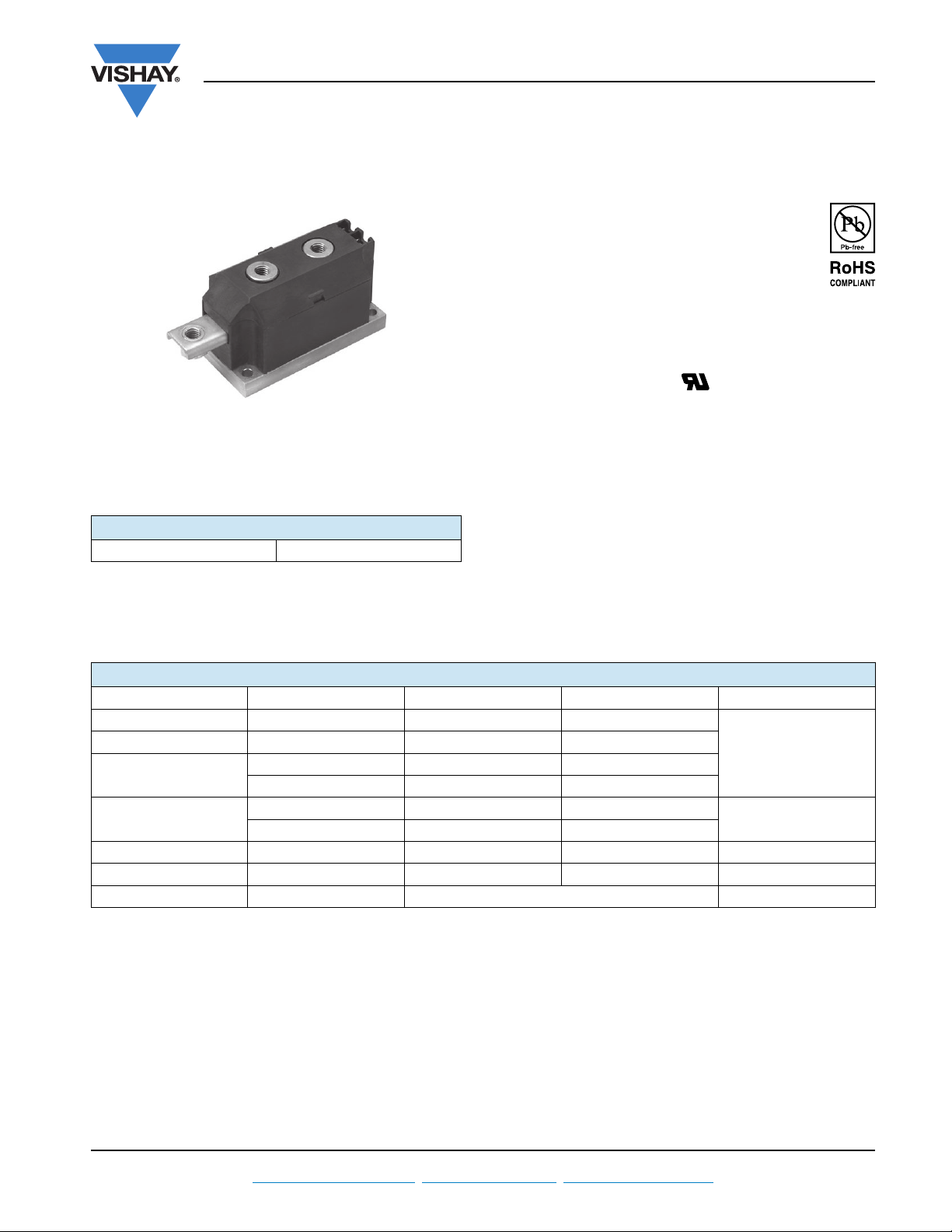
Vishay VSK.170PbF Series, VSK.250PbF Series Data Sheet

(MAGN-A-PAK Power Modules), 170 A/250 A
MAGN-A-PAK
PRODUCT SUMMARY
I
T(AV)
VSK.170PbF, VSK.250PbF Series
SCR/SCR and SCR/Diode
FEATURES
• High voltage
• Electrically isolated base plate
170 A/250 A
• 3500 V
• Industrial standard package
• Simplified mechanical designs, rapid assembly
• High surge capability
• Large creepage distances
• UL approved file E78996
• Compliant to RoHS directive 2002/95/EC
• Designed and qualified for industrial level
DESCRIPTION
This new VSK series of MAGN-A-PAK modules uses high
voltage power thyristor/thyristor and thyristor/diode in
seven basic configurations. The semiconductors are
electrically isolated from the metal base, allowing common
heatsinks and compact assemblies to be built. They can be
interconnected to form single phase or three phase bridges
or as AC-switches when modules are connected in
anti-parallel mode. These modules are intended for general
purpose applications such as battery chargers, welders,
motor drives, UPS, etc.
isolating voltage
RMS
Vishay Semiconductors
MAJOR RATINGS AND CHARACTERISTICS
SYMBOL CHARACTERISTICS VSK.170.. VSK.250.. UNITS
I
T(AV)
I
T(RMS)
I
TSM
2
t
I
2
I
t 1310 3610 kA2s
V
DRM/VRRM
T
J
85 °C 170 250
377 555
50 Hz 5100 8500
60 Hz 5350 8900
50 Hz 131 361
60 Hz 119 330
Up to 1600 Up to 2000 V
Range - 40 to 130 °C
kA2s
A
Document Number: 94417 For technical questions within your region, please contact one of the following: www.vishay.com
Revision: 02-Jul-10 DiodesAmericas@vishay.com
, DiodesAsia@vishay.com, DiodesEurope@vishay.com 1

VSK.170PbF, VSK.250PbF Series
Vishay Semiconductors
ELECTRICAL SPECIFICATIONS
VOLTAGE RATINGS
V
TYPE NUMBER
VSK.170-
VSK.250-
VOLTAGE
CODE
04 400 500
08 800 900
10 1000 1100
12 1200 1300
14 1400 1500
16 1600 1700
04 400 500
08 800 900
10 1000 1100
12 1200 1300
14 1400 1500
16 1600 1700
18 1800 1900
20 2000 2100
SCR/SCR and SCR/Diode
(MAGN-A-PAK Power Modules), 170 A/250 A
RRM/VDRM
, MAXIMUM REPETITIVE
PEAK REVERSE AND OFF-STATE
BLOCKING VOLTAGE
V
V
, MAXIMUM
RSM
NON-REPETITIVE PEAK
REVERSE VOLTAGE
V
I
RRM/IDRM
AT 130 °C
MAXIMUM
mA
50
50
60
ON-STATE CONDUCTION
PARAMETER SYMBOL TEST CONDITIONS VSK.170 VSK.250 UNITS
Maximum average on-state current
at case temperature
Maximum RMS on-state current I
Maximum peak, one-cycle on-state
non-repetitive, surge current
2
Maximum I
Maximum I
t for fusing I2t
2
t for fusing I2t t = 0.1 ms to 10 ms, no voltage reapplied 1310 3610 kA2s
Low level value or threshold voltage V
High level value of threshold voltage V
Low level value on-state slope resistance r
High level value on-state slope resistance r
Maximum on-state voltage drop V
Maximum holding current I
Maximum latching current I
I
T(AV)
T(RMS)
I
TSM
T(TO)1
T(TO)2
t1
(I > x I
t2
TM
H
L
180° conduction, half sine wave
As AC switch 377 555
t = 10 ms
t = 8.3 ms 5350 8900
t = 10 ms
t = 8.3 ms 4500 7500
t = 10 ms
t = 8.3 ms 119 330
t = 10 ms
t = 8.3 ms 84.4 233
(16.7 % x x I
T
= TJ maximum
J
(I > x I
T(AV)
(16.7 % x x I
T
= TJ maximum
J
T(AV)
ITM = x I
T(AV)
average power = V
No voltage
reapplied
100 % V
reapplied
No voltage
reapplied
100 % V
RRM
RRM
Sinusoidal
half wave,
initial T
=
J
maximum
T
J
reapplied
< I < x I
T(AV)
< I < x I
< I < x I
T(AV)
< I < x I
T(AV)
T(AV)
),
T(AV)
), TJ = TJ maximum 1.12 1.00
),
T(AV)
), TJ = TJ maximum 0.96 0.57
, TJ = TJ maximum, 180° conduction,
T(TO)
x I
T(AV)
+ rf x (I
T(RMS)
2
)
Anode supply = 12 V, initial IT = 30 A, TJ = 25 °C 500 500
Anode supply = 12 V, resistive load = 1 ,
gate pulse: 10 V, 100 μs, T
= 25 °C
J
www.vishay.com For technical questions within your region, please contact one of the following: Document Number: 94417
2 DiodesAmericas@vishay.com
, DiodesAsia@vishay.com, DiodesEurope@vishay.com Revision: 02-Jul-10
170 250 A
85 85 °C
5100 8500
4300 7150
131 361
92.5 255
kA2s
0.89 0.97
1.34 0.60
1.60 1.44 V
1000 1000
A
V
m
mA

VSK.170PbF, VSK.250PbF Series
SCR/SCR and SCR/Diode
Vishay Semiconductors
(MAGN-A-PAK Power Modules), 170 A/250 A
SWITCHING
PARAMETER SYMBOL TEST CONDITIONS VSK.170 VSK.250 UNITS
Typical delay time t
Typical rise time t
Typical turn-off time t
TJ = 25 °C, gate current = 1 A dIg/dt = 1 A/μs
d
= 0.67 % V
V
r
q
d
I
= 300 A; dI/dt = 15 A/μs; TJ = TJ maximum;
TM
V
= 50 V; dV/dt = 20 V/μs; gate 0 V, 100
R
DRM
BLOCKING
PARAMETER SYMBOL TEST CONDITIONS VSK.170 VSK.250 UNITS
Maximum peak reverse and
off-state leakage current
RMS insulation voltage V
Critical rate of rise of off-state voltage dV/dt T
I
RRM,
I
DRM
TJ = TJ maximum 50 60 mA
50 Hz, circuit to base, all terminals shorted, 25 °C, 1 s 3000 V
INS
= TJ maximum, exponential to 67 % rated V
J
DRM
TRIGGERING
PARAMETER SYMBOL TEST CONDITIONS VSK.170 VSK.250 UNITS
Maximum peak gate power P
Maximum average gate power P
GM
G(AV)
Maximum peak gate current + I
Maximum peak negative gate voltage - V
Maximum required DC gate voltage to trigger V
Maximum required DC gate current to trigger I
Maximum gate voltage that will not trigger V
Maximum gate current that willnot trigger I
GT
GT
GD
GD
Maximum rate of rise of turned-on current dI/dt
tp 5 ms, TJ = TJ maximum 10.0
f = 50 Hz, TJ = TJ maximum 2.0
tp 5 ms, TJ = TJ maximum 3.0 A
GM
tp 5 ms, TJ = TJ maximum 5.0
GT
TJ = - 40 °C
T
= 25 °C 3.0
J
= TJ maximum 2.0
T
J
Anode supply = 12 V,
resistive load; Ra = 1
TJ = - 40 °C
= 25 °C 200
J
= TJ maximum 100
T
J
TJ = TJ maximum, rated V
TJ = TJ maximum, rated V
= TJ maximum, ITM = 400 A,
T
J
rated V
DRM
applied
Anode supply = 12 V,
resistive load; Ra = 1
applied 0.25 V
DRM
applied 10.0 mA
DRM
1.0
2.0
50 to 150
1000 V/μs
4.0
350
mAT
500 A/μs
μs
W
V
THERMAL AND MECHANICAL SPECIFICATIONS
PARAMETER SYMBOL TEST CONDITIONS VSK.170 VSK.250 UNITS
Junction operating and storage
temperature range
Maximum thermal resistance,
junction to case per junction
Typical thermal resistance,
case to heatsink per module
MAP to heatsink
Mounting torque ± 10 %
busbar to MAP
Approximate weight
Case style MAGN-A-PAK
Document Number: 94417 For technical questions within your region, please contact one of the following: www.vishay.com
Revision: 02-Jul-10 DiodesAmericas@vishay.com
, T
T
J
Stg
DC operation 0.17 0.125
Mounting surface flat, smooth and greased 0.02 0.02
R
R
thJC
thCS
- 40 to 130 °C
A mounting compound is recommended
and the torque should be rechecked after
a period of about 3 hours to allow for the
4 to 6 Nm
spread of the compound.
500 g
17.8 oz.
, DiodesAsia@vishay.com, DiodesEurope@vishay.com 3
K/W

VSK.170PbF, VSK.250PbF Series
60
70
80
90
100
110
120
130
0 40 80 120 160 200
30°
60°
90°
120°
180°
Average On-st ate Current (A)
Maximum Allowable Case Temperature (°C)
Conduction Ang le
VSK.170.. Series
R
thJC
(DC) = 0.17 K/W
60
70
80
90
100
110
120
130
0 50 100 150 200 250 3
00
DC
30°
60°
90°
120°
180°
Average On-state Curr ent (A)
Maximum Allowable Case Temperature (°C)
Conduction Period
VSK.170.. Series
R (DC) = 0.17 K/W
thJC
0
50
100
150
200
250
300
350
0 50 100 150 200 250 3
00
DC
180°
120°
90°
60°
30°
RMS Limit
Conduction Period
Maximum Average On-state Power Loss (W)
Average On-state Current (A)
VSK.170.. Series
Per Junction
T
J
= 125°C
Vishay Semiconductors
SCR/SCR and SCR/Diode
(MAGN-A-PAK Power Modules), 170 A/250 A
R CONDUCTION PER JUNCTION
DEVICES
SINUSOIDAL CONDUCTION AT T
180° 120° 90° 60° 30° 180° 120° 90° 60° 30°
VSK.170- 0.009 0.010 0.010 0.020 0.032 0.007 0.011 0.015 0.020 0.033
VSK.250- 0.009 0.010 0.014 0.020 0.032 0.007 0.011 0.015 0.020 0.033
Note
• Table shows the increment of thermal resistance R
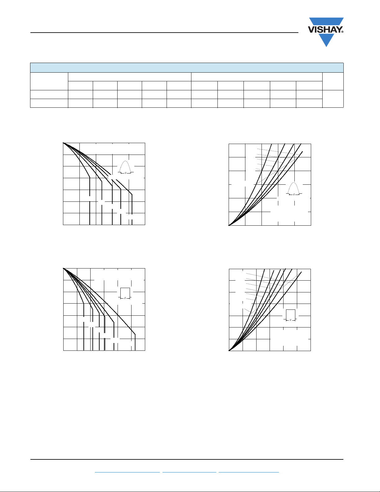
Fig. 1 - Current Ratings Characteristics
MAXIMUM RECTANGULAR CONDUCTION AT TJ MAXIMUM
J
when devices operate at different conduction angles than DC
thJC
)
300
250
200
150
100
50
0
Maximum Average On-state Power Loss (W
040801201602
180°
120°
90°
60°
30°
RMS Limit
VSK.170.. Series
Per Junction
T
J
Average On-state Current (A)
Conduction Angle
= 125°C
Fig. 3 - On-State Power Loss Characteristics
UNITS
K/W
00
Fig. 2 - Current Ratings Characteristics
www.vishay.com For technical questions within your region, please contact one of the following: Document Number: 94417
4 DiodesAmericas@vishay.com
Fig. 4 - On-State Power Loss Characteristics
, DiodesAsia@vishay.com, DiodesEurope@vishay.com Revision: 02-Jul-10
 Loading...