

VISHAY
Vishay Semiconductors
IR Receiver Modules for Remote Control Systems
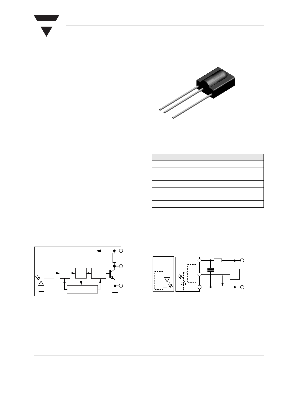
Description
The TSOP312.. - series are miniaturized receivers for
infrared remote control systems. PIN diode and
preamplifier are assembled on lead frame, the epoxy
package is designed as IR filter.
The demodulated output signal can directly be
decoded by a microprocessor. TSOP312.. is the standard IR remote control receiver series for 3 V supply
voltage, supporting all major transmission codes.
Features
• Photo detector and preamplifier in one package
• Internal filter for PCM frequency
1
2
3
94 8691
TSOP312..
• Improved shielding against electrical field
disturbance
• TTL and CMOS compatibility
• Output active low
• Supply voltage: 2.7 V to 5.5 V
• Improved immunity against ambient light
Mechanical Data
Pinning:
1 = GND
2 = V
S
3 = OUT
Block Diagram
16832
2
V
S
3
OUT
1
GND
PIN
AGCInput
Band
Pass
Control
30 kΩ
Demodulator
Circuit
Parts Table
Part Carrier Frequency
TSOP31230 30 kHz
TSOP31233 33 kHz
TSOP31236 36 kHz
TSOP31237 36.7 kHz
TSOP31238 38 kHz
TSOP31240 40 kHz
TSOP31256 56 kHz
Application Circuit
17170
Transmitter
with
TSALxxxx
R1+C1recommended to suppress power supply
disturbances.
The output voltage should not be hold continuously at
a voltage below V
TSOPxxxx
Circuit
=
2.0 V by the external circuit.
O
V
S
OUT
GND
R1=100Ω
C1=
4.7 µF
+V
µC
V
O
GND
S
Document Number 82217
Rev. 2, 19-May-03
www.vishay.com
1
TSOP312..
Vishay Semiconductors
Absolute Maximum Ratings
T
= 25 °C, unless otherwise specified
amb
Par ame te r Te s t co n di ti o n Symbol Va lu e Unit
Supply Voltage (Pin 2) V
Supply Current (Pin 2) I
Output Voltage (Pin 3) V
Output Current (Pin 3) I
Junction Temperature T
Storage Temperature Range T
Operating Temperature Range T
Power Consumption (T
Soldering Temperature t ≤ 10 s, 1 mm from case T
Electrical and Optical Characteristics
T
= 25 °C, unless otherwise specified
amb
V
= 3 V
S
Paramete r Test condition Symbol Min Typ . Max Unit
Supply Current (Pin 3) Ev = 0 I
Ev = 40 klx, sunlight I
Supply Voltage V
Transmission Distance Ev = 0, test signal see fig.1,
IR diode TSAL6200,
I
= 250 mA
F
Output Voltage Low (Pin 1)
Irradiance (30-40 kHz) VS = 3 V
Irradiance (56 kHz) VS = 3 V
Irradiance (30-40 kHz) VS = 5 V
Irradiance (56 kHz) VS = 5 V
Irradiance tpi - 5/fo < tpo < tpi + 6/fo,
Directivity Angle of half transmission
I
= 0.5 mA, Ee = 0.7 mW/m2,
OSL
test signal see fig. 1
Pulse width tolerance:
t
- 5/fo < tpo < tpi + 6/fo,
pi
test signal see fig.1
Pulse width tolerance:
t
- 5/fo < tpo < tpi + 6/fo,
pi
test signal see fig.1
Pulse width tolerance:
t
- 5/fo < tpo < tpi + 6/fo,
pi
test signal see fig.1
Pulse width tolerance:
t
- 5/fo < tpo < tpi + 6/fo,
pi
test signal see fig.1
test signal see fig. 1
distance
≤ 85 °C) P
amb
SD
SH
S
0.7 1.2 1.5 mA
2.7 5.5 V
d 35 m
V
OSL
E
e min
E
e min
E
e min
E
e min
E
e max
ϕ
1/2
30
VISHAY
S
S
O
O
j
stg
amb
tot
sd
1.3 mA
0.35 0.5
0.4 0.6
0.45 0.6
0.5 0.7
± 45 deg
- 0.3 to
+ 6.0
3 mA
- 0.3 to
(V
+ 0.3)
S
10 mA
100 °C
- 25 to + 85 °C
- 25 to + 85 °C
30 mW
260 °C
250 mV
mW/m
mW/m
mW/m
mW/m
W/m
V
V
2
2
2
2
2
www.vishay.com
2
Document Number 82217
Rev. 2, 19-May-03
VISHAY
TSOP312..
Vishay Semiconductors
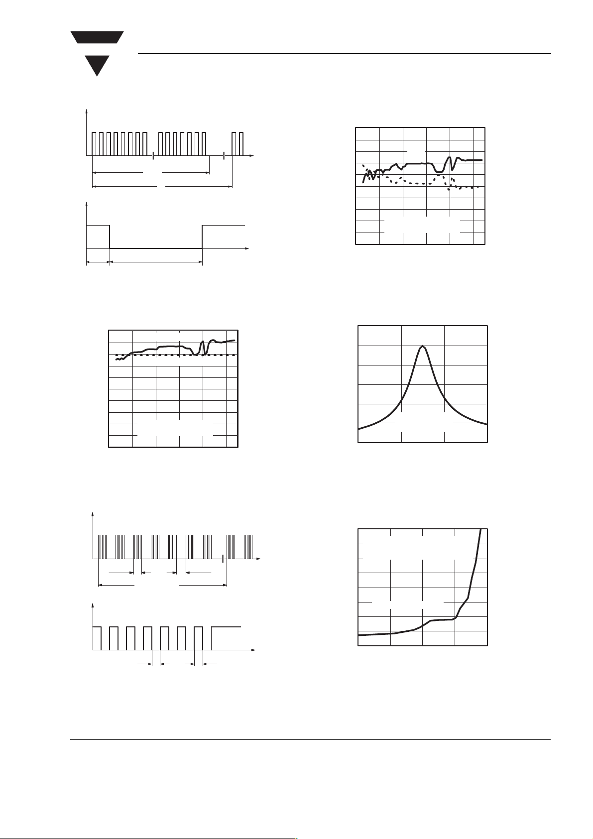
Typical Characteristics (T
Optical Test Signal
E
e
(IR diode TSAL6200, IF = 0.4 A, 30 pulses, f = f0, T = 10 ms)
amb
tpi *
T
* t
w 10/fo is recommended for optimal function
pi
Output Signal
V
O
V
OH
V
OL
1)
7/f0< td< 15/f
2)
tpi–5/f0< tpo < tpi+6/f
1)
t
d
0
0
2)
t
po
Figure 1. Output Function
1.0
0.9
0.8
0.7
0.6
0.5
0.4
0.3
0.2
po
0.1
t – Output Pulse Width ( ms )
0.0
0.1 1.0 10.0 100.0 1000.010000.0
16908
Output Pulse
Input Burst Duration
l = 950 nm,
optical test signal, fig.1
Ee – Irradiance ( mW/m2 )
= 25 °C unless otherwise specified)
1.0
0.9
t
16110
t
0.8
0.7
0.6
0.5
0.4
0.3
0.2
0.1
on off
T ,T – Output Pulse Width ( ms )
0.0
0.1 1.0 10.0 100.0 1000.010000.0
16909
Figure 4. Output Pulse Diagram
1.2
1.0
0.8
0.6
0.4
0.2
e min e
E / E – Rel. Responsivity
0.0
0.7 0.9 1.1 1.3
16925
To n
To ff
l = 950 nm,
optical test signal, fig.3
Ee – Irradiance ( mW/m2 )
f = f0"5%
Df ( 3dB ) = f
f/f0 – Relative Frequency
/10
0
Figure 2. Pulse Length and Sensitivity in Dark Ambient
Optical Test Signal
E
e
600 ms 600 ms
T = 60 ms
Output Signal, ( see Fig.4 )
V
O
V
OH
V
OL
T
on
T
off
Figure 3. Output Function
Document Number 82217
Rev. 2, 19-May-03
94 8134
t
Figure 5. Frequency Dependence of Responsivity
4.0
2
t
e min
E – Threshold Irradiance ( mW/m )
16911
Correlation with ambient light sources:
3.5
3.0
2.5
2.0
1.5
1.0
0.5
0.0
0.01 0.10 1.00 10.00 100.00
2
10W/m
^1.4klx (Std.illum.A,T=2855K)
2
10W/m
^8.2klx (Daylight,T=5900K)
Ambient, l = 950 nm
E – Ambient DC Irradiance (W/m2)
Figure 6. Sensitivity in Bright Ambient
www.vishay.com
3
TSOP312..
Vishay Semiconductors
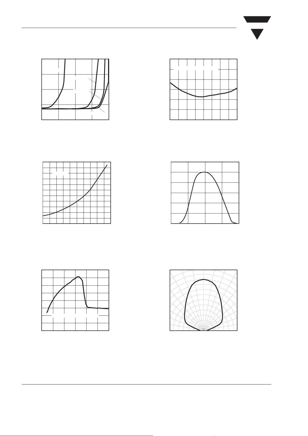
VISHAY
2.0
2
f = f
1.5
1.0
0.5
e min
E – Threshold Irradiance ( mW/m )
0.0
0.1 1.0 10.0 100.0 1000.0
16912
DV
sRMS
o
f = 10 kHz
f = 1 kHz
f = 100 Hz
– AC Voltage on DC Supply Voltage (mV)
Figure 7. Sensitivity vs. Supply Voltage Disturbances
2
2.0
f(E) = f
1.6
1.2
0.8
0.4
e min
E – Threshold Irradiance ( mW/m )
0.0
0.0 0.4 0.8 1.2 1.6
94 8147
E – Field Strength of Disturbance ( kV/m )
0
2.0
0.6
2
Sensitivity in dark ambient
0.5
0.4
0.3
0.2
0.1
e min
E – Threshold Irradiance ( mW/m )
0.0
–30–150 153045607590
T
16918
– Ambient Temperature ( qC )
amb
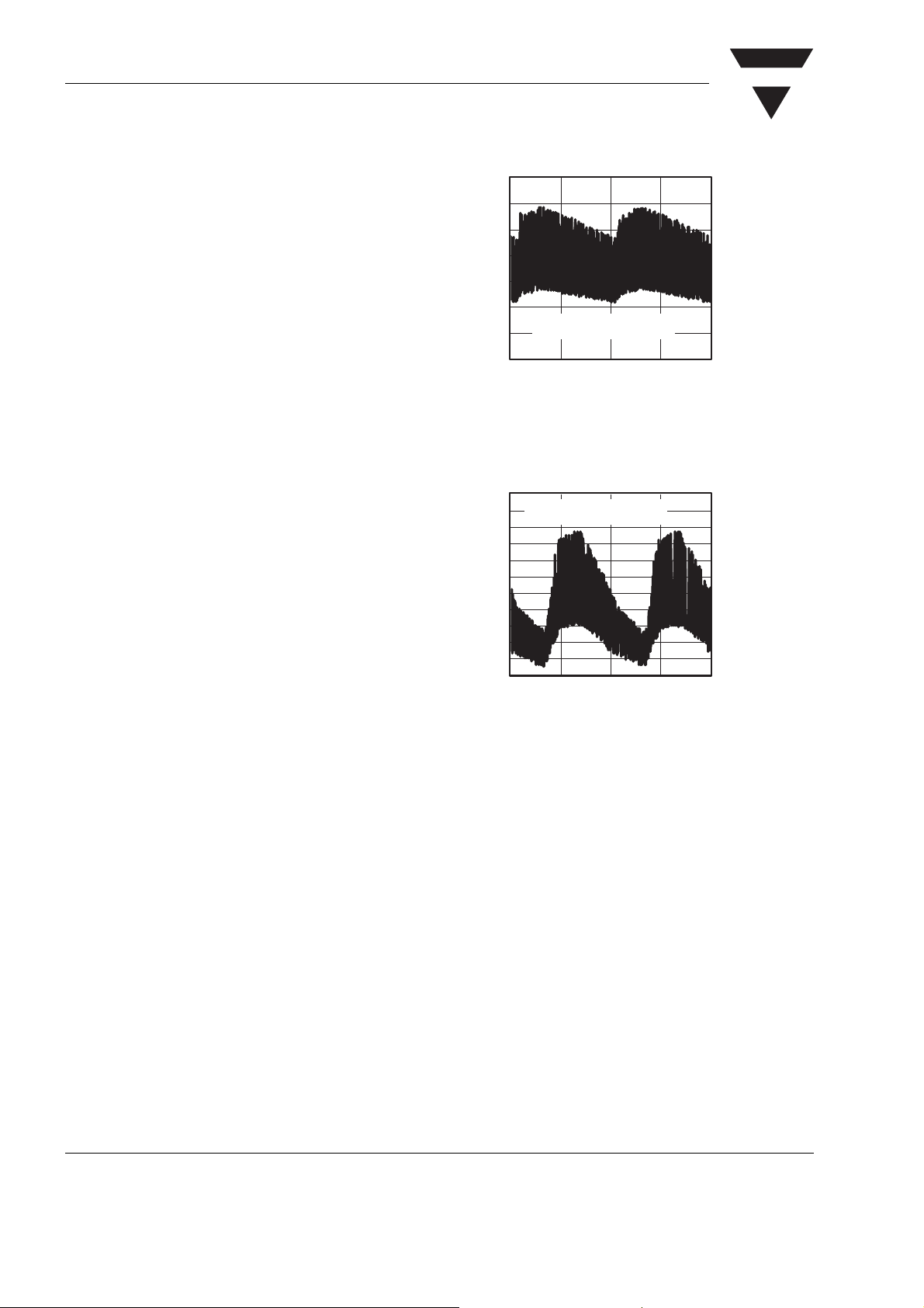
Figure 10. Sensitivity vs. Ambient Temperature
1.2
1.0
0.8
0.6
0.4
rel
0.2
l
S ( ) – Relative Spectral Sensitivity
0
750 850 950 1050
94 8408
l – Wavelength ( nm )
1150
Figure 8. Sensitivity vs. Electric Field Disturbances
0.8
0.7
0.6
0.5
0.4
0.3
0.2
Max. Envelope Duty Cycle
0.1
0.0
16913
f = 38 kHz, Ee = 2 mW/m
0 20 40 60 80 100 120
Burst Length ( number of cycles / burst )
2
Figure 9. Max. Envelope Duty Cycle vs. Burstlength
www.vishay.com
4
Figure 11. Relative Spectral Sensitivity vs. Wavelength
0°
1.0
0.9
0.8
0.7
95 11340p2
10° 20°
0.4 0.2 0 0.2 0.4
0.6
d
- Relative Transmission Distance
rel
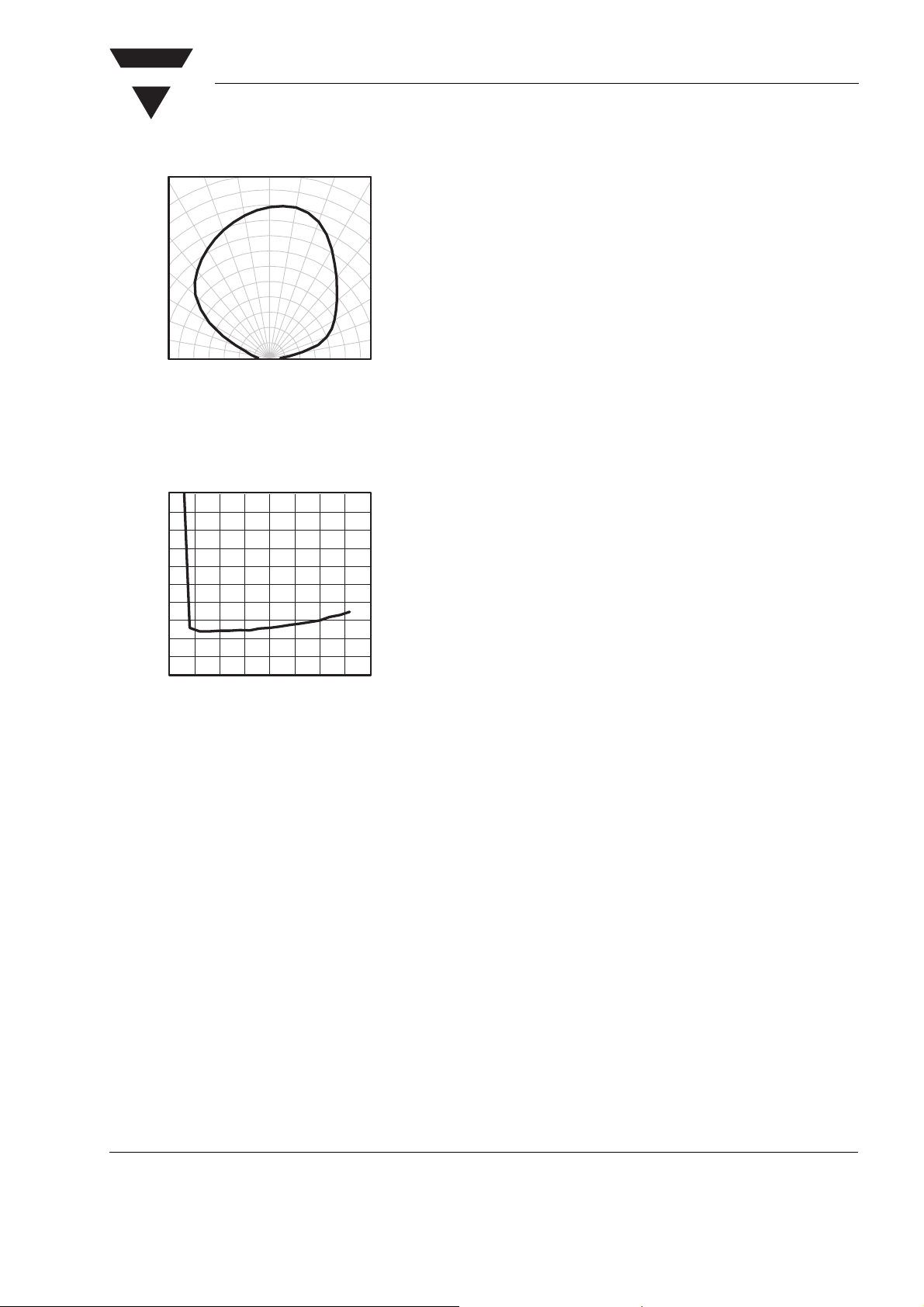
Figure 12. Horizontal Directivity ϕ
30°
40°
50°
60°
70°
80°
0.6
x
Document Number 82217
Rev. 2, 19-May-03
VISHAY
0°
10° 20°
TSOP312..
Vishay Semiconductors
30°
1.0
0.9
0.8
0.7
0.4 0.2 0 0.2 0.4
0.6
d
95 11339p2
- Relative Transmission Distance
rel
Figure 13. Vertical Directivity ϕ
1.0
0.9
2
0.8
0.7
0.6
0.5
0.4
0.3
e min
0.2
E – Sensitivity ( mW/m )
0.1
0.0
2.0 2.5 3.0 3.5 4.0 4.5 5.0 5.5 6.0
17185
VS – Supply Voltage ( V )
40°
50°
60°
70°
80°
0.6
y
Figure 14. Sensitivity vs. Supply Voltage
Document Number 82217
Rev. 2, 19-May-03
www.vishay.com
5
TSOP312..
Vishay Semiconductors
Suitable Data Format
The circuit of the TSOP312.. is designed in that way
that unexpected output pulses due to noise or disturbance signals are avoided. A bandpass filter, an integrator stage and an automatic gain control are used
to suppress such disturbances.
The distinguishing mark between data signal and disturbance signal are carrier frequency, burst length
and duty cycle.
The data signal should fulfill the following conditions:
• Carrier frequency should be close to center frequency of the bandpass (e.g. 38 kHz).
• Burst length should be 10 cycles/burst or longer.
• After each burst which is between 10 cycles and 70
cycles a gap time of at least 14 cycles is necessary.
• For each burst which is longer than 1.8 ms a corresponding gap time is necessary at some time in the
data stream. This gap time should be at least 4 times
longer than the burst.
• Up to 800 short bursts per second can be received
continuously.
Some examples for suitable data format are: NEC
Code (repetitive pulse), NEC Code (repetitive data),
Toshiba Micom Format, Sharp Code, RC5 Code,
RC6 Code, R-2000 Code, Sony Code.
When a disturbance signal is applied to the
TSOP312.. it can still receive the data signal. However the sensitivity is reduced to that level that no
unexpected pulses will occur.
Some examples for such disturbance signals which
are suppressed by the TSOP312.. are:
• DC light (e.g. from tungsten bulb or sunlight)
• Continuous signal at 38 kHz or at any other frequency
• Signals from fluorescent lamps with electronic ballast with high or low modulation
( see Figure 15 or Figure 16 ).
VISHAY
IR Signal
IR Signal from fluorescent
lamp with low modulation
0 5 10 15 20
16920
Figure 15. IR Signal from Fluorescent Lamp with low Modulation
IR Signal from fluorescent
lamp with high modulation
IR Signal
0 5 10 15 20
16921
Figure 16. IR Signal from Fluorescent Lamp with high Modulation
Time ( ms )
Time ( ms )
www.vishay.com
6
Document Number 82217
Rev. 2, 19-May-03

VISHAY
Package Dimensions in mm
TSOP312..
Vishay Semiconductors
+0.1
96 12116
Document Number 82217
Rev. 2, 19-May-03
www.vishay.com
7

TSOP312..
VISHAY
Vishay Semiconductors
Ozone Depleting Substances Policy Statement
It is the policy of Vishay Semiconductor GmbH to
1. Meet all present and future national and international statutory requirements.
2. Regularly and continuously improve the performance of our products, processes, distribution and
operatingsystems with respect to their impact on the health and safety of our employees and the public, as
well as their impact on the environment.
It is particular concern to control or eliminate releases of those substances into the atmosphere which are
known as ozone depleting substances (ODSs).
The Montreal Protocol (1987) and its London Amendments (1990) intend to severely restrict the use of ODSs
and forbid their use within the next ten years. Various national and international initiatives are pressing for an
earlier ban on these substances.
Vishay Semiconductor GmbH has been able to use its policy of continuous improvements to eliminate the
use of ODSs listed in the following documents.
1. Annex A, B and list of transitional substances of the Montreal Protocol and the London Amendments
respectively
2. Class I and II ozone depleting substances in the Clean Air Act Amendments of 1990 by the Environmental
Protection Agency (EPA) in the USA
3. Council Decision 88/540/EEC and 91/690/EEC Annex A, B and C (transitional substances) respectively.
Vishay Semiconductor GmbH can certify that our semiconductors are not manufactured with ozone depleting
substances and do not contain such substances.
We reserve the right to make changes to improve technical design
and may do so without further notice.
Parameters can vary in different applications. All operating parameters must be validated for each
customer application by the customer. Should the buyer use Vishay Semiconductors products for any
unintended or unauthorized application, the buyer shall indemnify Vishay Semiconductors against all
claims, costs, damages, and expenses, arising out of, directly or indirectly, any claim of personal
damage, injury or death associated with such unintended or unauthorized use.
Vishay Semiconductor GmbH, P.O.B. 3535, D-74025 Heilbronn, Germany
Telephone: 49 (0)7131 67 2831, Fax number: 49 (0)7131 67 2423
www.vishay.com
8
Document Number 82217
Rev. 2, 19-May-03

This datasheet has been download from:
www.datasheetcatalog.com
Datasheets for electronics components.
 Loading...