

TSML1000 / 1020 / 1030 / 1040
Vishay Semiconductors
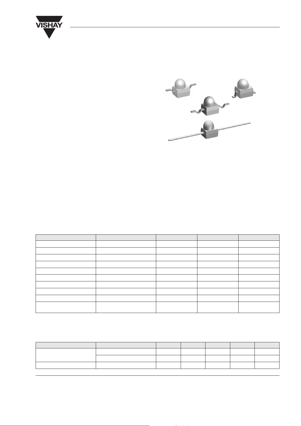
High Power Infrared Emitting Diode, 950 nm, GaAlAs/GaAs
Description
TSML1000 series are high efficiency infrared emitting
diodes in GaAlAs on GaAs technology molded in
clear SMD package.
This technology represents best performance for radiant power under pulse conditions, forward voltage
and reliability.
Features
• Outstanding high radiant power
• Low forward voltage
• Suitable for high pulse current operation
• Angle of half intensity ϕ = ± 12°
• Peak wavelength λ
• High reliability
• Matched Phototransistor series: TEMT1000
• Versatile terminal configurations
• Lead-free component
= 950 nm
p
TSML1000
TSML1030
TSML1020
TSML1040
16852
• Component in accordance to RoHS 2002/95/EC
and WEEE 2002/96/EC
Applications
For remote control
Photointerrupters
Punched tape readers
Encoder
Absolute Maximum Ratings
T
= 25 °C, unless otherwise specified
amb
Parameter Test condition Symbol Val ue Unit
Reverse Voltage V
Forward current I
Peak Forward Current t
Surge Forward Current t
Power Dissipation P
Junction Temperature T
Operating Temperature Range T
Storage Temperature Range T
Soldering Temperature t ≤ 5 sec T
Thermal Resistance Junction/
Ambient
/T = 0.5, tp = 100 µsIFM200 mA
p
= 100 µsI
p
Basic Characteristics
T
= 25 °C, unless otherwise specified
amb
T
= 25 °C, unless otherwise specified
amb
Parameter Test condition Symbol Min Ty p. Max Unit
Forward Voltage I
Temp. Coefficient of V
F
= 20 mA, tp = 20 ms V
F
I
= 1 A, tp = 100 µsV
F
IF = 1 mA TK
F
F
VF
R
F
FSM
amb
stg
sd
thJA
R
V
j
5V
100 mA
1.0 A
190 mW
100 °C
- 40 to + 85 °C
- 40 to + 100 °C
<260 °C
400 °C
1.2 1.5 V
2.6 V
- 1.85 mV/K
Document Number 81033
Rev. 1.8, 08-Mar-05
www.vishay.com
1
TSML1000 / 1020 / 1030 / 1040
VISHAY
Vishay Semiconductors
Parameter Test condition Symbol Min Ty p. Max Unit
Reverse Current VR = 5 V I
Junction capacitance V
Radiant Intensity I
Radiant Power I
Temp. Coefficient of φ
e
= 0 V, f = 1 MHz, E = 0 C
R
= 20 mA, tp = 20 ms I
F
= 100 mA, tp = 20 ms φ
F
IF = 20 mA TKφ
R
j
e
e
e
3715mW/sr
25 pF
35 mW
- 0.6 %/K
10 µA
Angle of Half Intensity ϕ ±12 deg
Peak Wavelength I
Spectral Bandwidth I
Temp. Coefficient of λ
p
Rise Time I
Fall Time I
= 100 mA λ
F
= 100 mA ∆λ 50 nm
F
IF = 100 mA TKλ
= 100 mA t
F
= 100 mA t
F
p
p
r
f
950 nm
0.2 nm/K
800 ns
800 ns
Virtual Source Diameter ∅ 1.2 mm
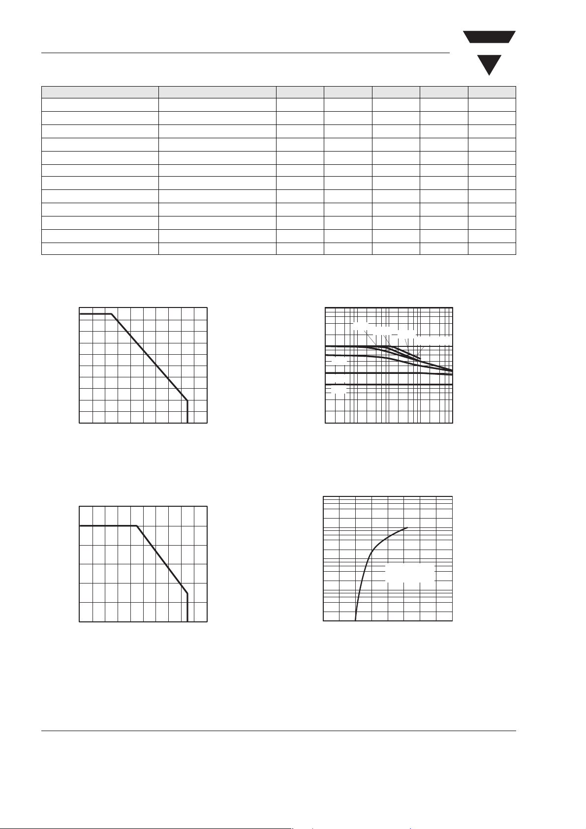
Typical Characteristics (Tamb = 25 °C unless otherwise specified)
200
180
160
140
120
100
80
60
40
V
P - Power Dissipation ( mW )
20
16187
0
T
- Ambient Temperature ( ° C)
amb
1009080706050403020100
Figure 1. Power Dissipation vs. Ambient Temperature
120
100
80
60
40
F
I - Forward Current ( mA )
20
10000
0.1
0.05
0.02
1000
0.2
0.5
100
1.0
10
0.01 0.10 1.00 10.00 100.00
tp- Pulse Duration ( ms )
14335
F
I - Forward Current ( mA )
tp/T = 0.01
Figure 3. Pulse Forward Current vs. Pulse Duration
4
10
3
10
2
10
t
1
10
F
I - Forward Current ( mA )
p
tp= 100 s
/T = 0.001
µ
0
T
16188
- Ambient Temperature ( ° C)
amb
Figure 2. Forward Current vs. Ambient Temperature
www.vishay.com
2
0
13600
10
43210
VF- Forward Voltage(V)
1009080706050403020100
Figure 4. Forward Current vs. Forward Voltage
Document Number 81033
Rev. 1.8, 08-Mar-05
VISHAY
TSML1000 / 1020 / 1030 / 1040
Vishay Semiconductors
1.2
1.1
IF=10mA
1.0
0.9
0.8
Frel
V - Relative Forward Voltage
94 7990
0.7
T
- Ambient Temperature ( °C)
amb
100806040200
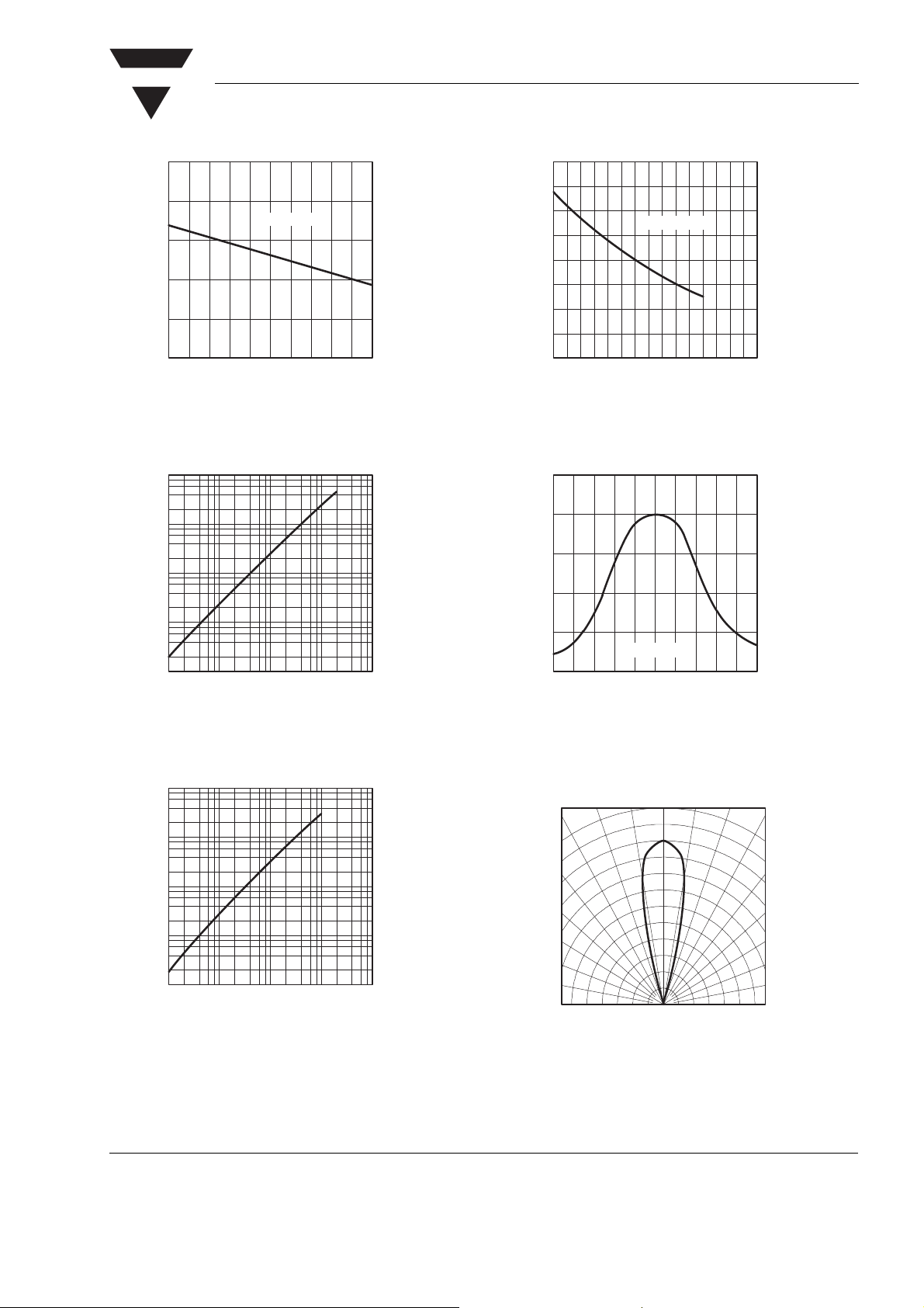
Figure 5. Relative Forward Voltage vs. Ambient Temperature
1000
100
10
1
e
I - Radiant Intensity ( mW/sr )
16189
0.1
10
0
1
10
I
- Forward Current ( mA )
F
10
2
10
3
10
4
1.6
1.2
IF=20mA
Φ
0.8
e rel e rel
I;
0.4
0
-10 10 500 100
T
94 7993
- Ambient Temperature ( °C)
amb
140
Figure 8. Rel. Radiant Intensity/Power vs. Ambient Temperature
1.25
1.0
0.75
0.5
- Relative Radiant Power
0.25
e rel
Φ
0
900 950
94 7994
IF= 100 mA
-
Wavelength ( nm )
λ
1000
Figure 6. Radiant Intensity vs. Forward Current
1000
100
10
- Radiant Power ( mW )
1
e
Φ
0.1
1
10
IF- Forward Current ( mA )
13602
10
0
Figure 7. Radiant Power vs. Forward Current
Document Number 81033
Rev. 1.8, 08-Mar-05
10
Figure 9. Relative Radiant Power vs. Wavelength
0 °°°
10 20
30°
40°
1.0
0.9
0.8
rel
S - Relative Intensity
0.7
10
3
10
4
0.4 0.2 0 0.2 0.4
18234
0.6
2
50°
60°
70°
80°
0.6
Figure 10. Relative Radiant Intensity vs. Angular Displacement
www.vishay.com
3

TSML1000 / 1020 / 1030 / 1040
Vishay Semiconductors
Package Dimensions in mm
TSML1000
VISHAY
Package Dimensions in mm
TSML1020
16159
www.vishay.com
4
16160
Document Number 81033
Rev. 1.8, 08-Mar-05

VISHAY
Package Dimensions in mm
TSML1030
TSML1000 / 1020 / 1030 / 1040
Vishay Semiconductors
Package Dimensions in mm
TSML1040
16228
16760
Document Number 81033
Rev. 1.8, 08-Mar-05
www.vishay.com
5

TSML1000 / 1020 / 1030 / 1040
Vishay Semiconductors
Reel Dimensions
VISHAY
www.vishay.com
6
18033
Document Number 81033
Rev. 1.8, 08-Mar-05

VISHAY
Taping TSML1000
TSML1000 / 1020 / 1030 / 1040
Vishay Semiconductors
Taping TSML1020
18030
Document Number 81033
Rev. 1.8, 08-Mar-05
18031
www.vishay.com
7

TSML1000 / 1020 / 1030 / 1040
Vishay Semiconductors
Taping TSML1030
VISHAY
Precautions For Use
1. Over-current-proof
Customer must apply resistors for protection, otherwise slight voltage shift will cause big current change
(Burn out will happen).
2. Storage
2.1 Storage temperature and rel. humidity conditions
are: 5 °C to 35 °C, R.H. 60 %
2.2 Floor life must not exceed 168 h, acc. to JEDEC
level 3, J-STD-020.
Once the package is opened, the products should be
used within a week. Otherwise, they should be kept in
a damp proof box with desiccant.
Considering tape life, we suggest to use products
within one year from production date.
2.3 If opened more than one week in an atmosphere
5 °C to 35 °C, R.H. 60 %, devices should be treated
at 60°C ± 5°C for 15 hrs.
2.4 If humidity indicator in the package shows pink
color (normal blue), then devices should be treated
with the same conditions as 2.3
Reflow Solder Profile
260
240
220
200
°
180
160
140
120
Temperature ( C )
100
80
60
02040 60 80 100 120 140160 180 200 220
17172
+5°C/s
60 sto120 s
Time(s)
18032
-5 °C/s
5s
www.vishay.com
8
Document Number 81033
Rev. 1.8, 08-Mar-05

VISHAY
TSML1000 / 1020 / 1030 / 1040
Vishay Semiconductors
Ozone Depleting Substances Policy Statement
It is the policy of Vishay Semiconductor GmbH to
1. Meet all present and future national and international statutory requirements.
2. Regularly and continuously improve the performance of our products, processes, distribution and
operatingsystems with respect to their impact on the health and safety of our employees and the public, as
well as their impact on the environment.
It is particular concern to control or eliminate releases of those substances into the atmosphere which are
known as ozone depleting substances (ODSs).
The Montreal Protocol (1987) and its London Amendments (1990) intend to severely restrict the use of ODSs
and forbid their use within the next ten years. Various national and international initiatives are pressing for an
earlier ban on these substances.
Vishay Semiconductor GmbH has been able to use its policy of continuous improvements to eliminate the use
of ODSs listed in the following documents.
1. Annex A, B and list of transitional substances of the Montreal Protocol and the London Amendments
respectively
2. Class I and II ozone depleting substances in the Clean Air Act Amendments of 1990 by the Environmental
Protection Agency (EPA) in the USA
3. Council Decision 88/540/EEC and 91/690/EEC Annex A, B and C (transitional substances) respectively.
Vishay Semiconductor GmbH can certify that our semiconductors are not manufactured with ozone depleting
substances and do not contain such substances.
We reserve the right to make changes to improve technical design
and may do so without further notice.
Parameters can vary in different applications. All operating parameters must be validated for each
customer application by the customer. Should the buyer use Vishay Semiconductors products for any
unintended or unauthorized application, the buyer shall indemnify Vishay Semiconductors against all
claims, costs, damages, and expenses, arising out of, directly or indirectly, any claim of personal
damage, injury or death associated with such unintended or unauthorized use.
Vishay Semiconductor GmbH, P.O.B. 3535, D-74025 Heilbronn, Germany
Telephone: 49 (0)7131 67 2831, Fax number: 49 (0)7131 67 2423
Document Number 81033
Rev. 1.8, 08-Mar-05
www.vishay.com
9

Legal Disclaimer Notice
Vishay
Document Number: 91000 www.vishay.com
Revision: 08-Apr-05 1
Notice
Specifications of the products displayed herein are subject to change without notice. Vishay Intertechnology, Inc.,
or anyone on its behalf, assumes no responsibility or liability for any errors or inaccuracies.
Information contained herein is intended to provide a product description only. No license, express or implied, by
estoppel or otherwise, to any intellectual property rights is granted by this document. Except as provided in Vishay's
terms and conditions of sale for such products, Vishay assumes no liability whatsoever, and disclaims any express
or implied warranty, relating to sale and/or use of Vishay products including liability or warranties relating to fitness
for a particular purpose, merchantability, or infringement of any patent, copyright, or other intellectual property right.
The products shown herein are not designed for use in medical, life-saving, or life-sustaining applications.
Customers using or selling these products for use in such applications do so at their own risk and agree to fully
indemnify Vishay for any damages resulting from such improper use or sale.
 Loading...