


TSAL4400
Vishay Semiconductors
High Power Infrared Emitting Diode, 950 nm, GaAlAs/GaAs
Description
TSAL4400 is a high efficiency infrared emitting diode
in GaAlAs on GaAs technology, molded in clear, bluegrey tinted plastic packages.
In comparison with the standard GaAs on GaAs technology these emitters achieve about 100 % radiant
power improvement at a similar wavelength.
The forward voltages at low current and at high pulse
current roughly correspond to the low values of the
standard technology. Therefore these emitters are
ideally suitable as high performance replacements of
standard emitters.
94 8488
Features
• Extra high radiant power
• Low forward voltage
• Suitable for high pulse current operation
Applications
Infrared remote control units
Free air transmission systems
Infrared source for optical counters and card readers
• Standard T-1 (∅ 3 mm) package
• Angle of half intensity ϕ = ± 25°
• Peak wavelength λ
= 940 nm
p
• High reliability
• Good spectral matching to Si photodetectors
• Lead-free component
• Component in accordance to RoHS 2002/95/EC
and WEEE 2002/96/EC
Absolute Maximum Ratings
T
= 25 °C, unless otherwise specified
amb
Parameter Test condition Symbol Val ue Unit
Reverse Voltage V
Forward current I
Peak Forward Current t
Surge Forward Current t
Power Dissipation P
Junction Temperature T
Operating Temperature Range T
Storage Temperature Range T
Soldering Temperature t ≤ 5 sec, 2 mm from case T
Thermal Resistance Junction/
Ambient
/T = 0.5, tp = 100 µsIFM200 mA
p
= 100 µsI
p
R
F
FSM
amb
stg
sd
thJA
R
V
j
5V
100 mA
1.5 A
210 mW
100 °C
- 55 to + 100 °C
- 55 to + 100 °C
260 °C
350 K/W
Document Number 81006
Rev. 1.5, 08-Mar-05
www.vishay.com
1
TSAL4400
Vishay Semiconductors
Basic Characteristics
T
= 25 °C, unless otherwise specified
amb
Parameter Test condition Symbol Min Ty p. Max Unit
Forward Voltage I
Temp. Coefficient of V
F
Reverse Current V
Junction capacitance V
Radiant Intensity I
Radiant Power I
Temp. Coefficient of φ
e
= 100 mA, tp = 20 ms V
F
I
= 1 A, tp = 100 µsV
F
IF = 100 mA TK
= 5 V I
R
= 0 V, f = 1 MHz, E = 0 C
R
= 100 mA, tp = 20 ms I
F
I
= 1.0 A, tp = 100 µsIe135 240 mW/sr
F
= 100 mA, tp = 20 ms φ
F
IF = 20 mA TKφ
F
F
VF
R
j
e
e
e
16 30 80 mW/sr
Angle of Half Intensity ϕ ± 25 deg
Peak Wavelength I
Spectral Bandwidth I
Temp. Coefficient of λ
p
Rise Time I
Fall Time I
= 100 mA λ
F
= 100 mA ∆λ 50 nm
F
IF = 100 mA TKλ
= 100 mA t
F
= 100 mA t
F
p
p
r
f
Virtual Source Diameter method: 63 % encircled energy ∅ 1.9 mm
1.35 1.6 V
2.6 3 V
- 1.3 mV/K
10 µA
25 pF
35 mW
- 0.6 %/K
940 nm
0.2 nm/K
800 ns
800 ns
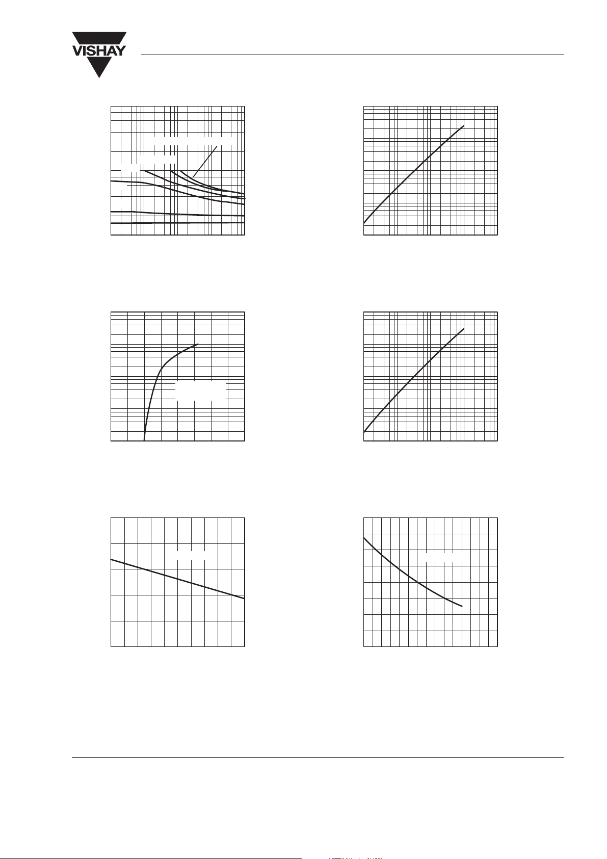
Typical Characteristics (Tamb = 25 °C unless otherwise specified)
250
200
150
R
thJA
100
50
V
P - Power Dissipation ( mW )
0
20 40 60 80 1000
T
94 7957
- Ambient Temperature ( °C)
amb
Figure 1. Power Dissipation vs. Ambient Temperature
250
200
150
100
R
F
I – Forward Current ( mA )
50
0
020406080
T
96 11986
– Ambient Temperature ( °C )
amb
thJA
Figure 2. Forward Current vs. Ambient Temperature
100
www.vishay.com
2
Document Number 81006
Rev. 1.5, 08-Mar-05
TSAL4400
Vishay Semiconductors
1
10
I
=1A(Single Pulse )
FSM
tp/T=0.01
0
0.05
10
0.1
F
I – Forward Current ( A)
0.5
1.0
–1
96 11987
10
10
10
–1
–2
10
0
tp– Pulse Duration ( ms )
10
1
10
Figure 3. Pulse Forward Current vs. Pulse Duration
4
10
3
10
2
10
t
1
10
F
I - Forward Current ( mA )
p
tp= 100 s
/T = 0.001
µ
1000
100
10
1
e
I – Radiant Intensity ( mW/sr )
0.1
2
14309
10
0
1
10
I
– Forward Current ( mA )
F
10
2
10
3
10
4
Figure 6. Radiant Intensity vs. Forward Current
1000
100
10
- Radiant Power ( mW )
1
e
Φ
0
13600
10
VF- Forward Voltage(V)
43210
Figure 4. Forward Current vs. Forward Voltage
1.2
1.1
IF=10mA
1.0
0.9
0.8
Frel
V - Relative Forward Voltage
94 7990
0.7
T
- Ambient Temperature ( ° C)
amb
100806040200
Figure 5. Relative Forward Voltage vs. Ambient Temperature
0.1
13602
10
0
10
1
IF- Forward Current ( mA )
10
2
10
3
10
4
Figure 7. Radiant Power vs. Forward Current
1.6
1.2
IF=20mA
Φ
0.8
e rel e rel
I;
0.4
0
-10 10 500 100
T
94 7993
- Ambient Temperature ( ° C)
amb
140
Figure 8. Rel. Radiant Intensity/Power vs. Ambient Temperature
Document Number 81006
Rev. 1.5, 08-Mar-05
www.vishay.com
3
TSAL4400
Vishay Semiconductors
1.25
1.0
0.75
0.5
– Relative Radiant Power
e rel
0.25
Φ
IF= 100 mA
0
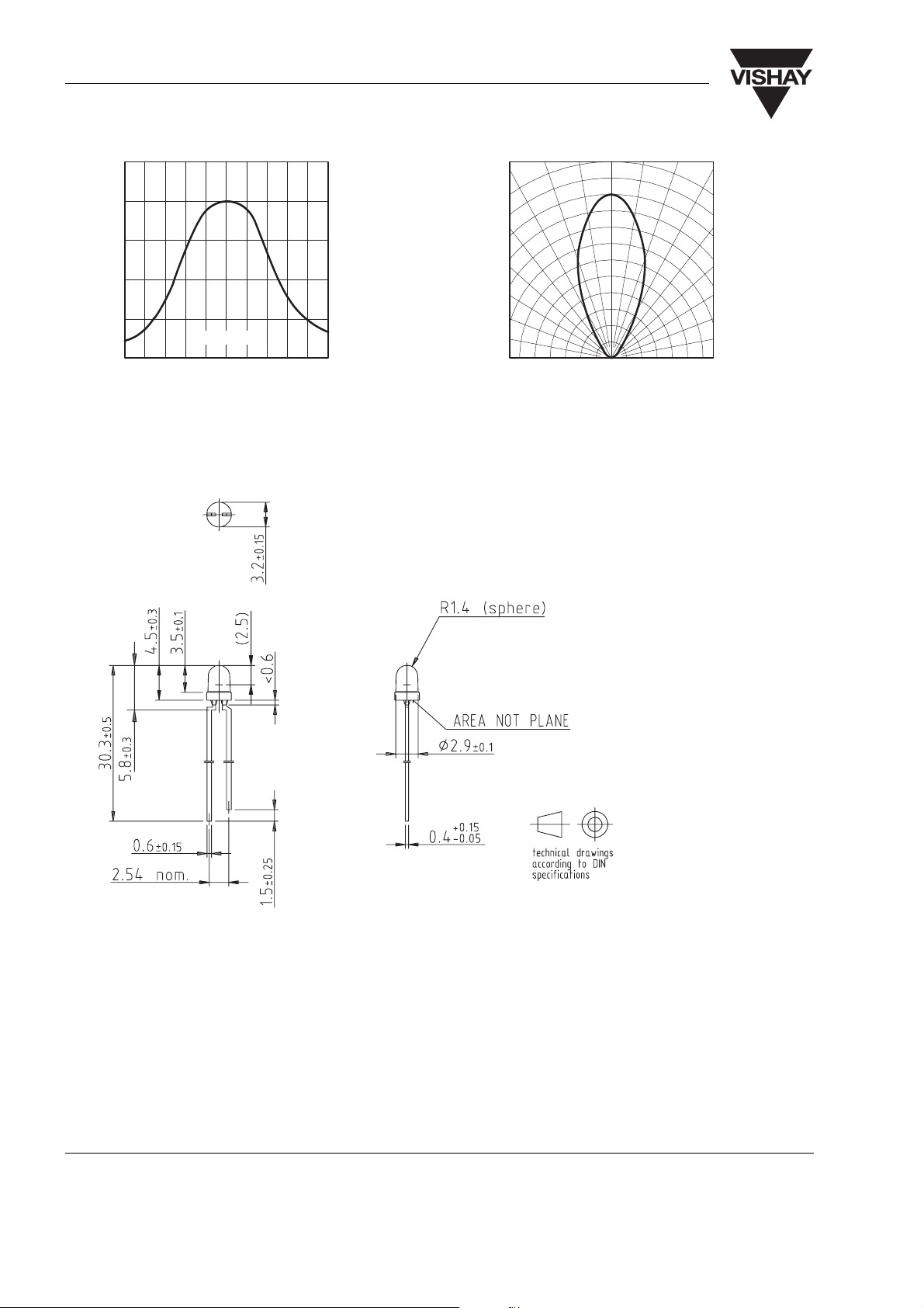
890 940
14291
– Wavelength ( nm )
λ
990
e rel
I – Relative Radiant Intensity
14328
1.0
0.9
0.8
0.7
0°
0.4 0.2 0 0.2 0.4
0.6
10°20
°
30°
40°
50°
60°
70°
80°
0.6
Figure 9. Relative Radiant Power vs. Wavelength
Package Dimensions in mm
Figure 10. Relative Radiant Intensity vs. Angular Displacement
95 10913
www.vishay.com
4
Document Number 81006
Rev. 1.5, 08-Mar-05

TSAL4400
Vishay Semiconductors
Ozone Depleting Substances Policy Statement
It is the policy of Vishay Semiconductor GmbH to
1. Meet all present and future national and international statutory requirements.
2. Regularly and continuously improve the performance of our products, processes, distribution and
operatingsystems with respect to their impact on the health and safety of our employees and the public, as
well as their impact on the environment.
It is particular concern to control or eliminate releases of those substances into the atmosphere which are
known as ozone depleting substances (ODSs).
The Montreal Protocol (1987) and its London Amendments (1990) intend to severely restrict the use of ODSs
and forbid their use within the next ten years. Various national and international initiatives are pressing for an
earlier ban on these substances.
Vishay Semiconductor GmbH has been able to use its policy of continuous improvements to eliminate the use
of ODSs listed in the following documents.
1. Annex A, B and list of transitional substances of the Montreal Protocol and the London Amendments
respectively
2. Class I and II ozone depleting substances in the Clean Air Act Amendments of 1990 by the Environmental
Protection Agency (EPA) in the USA
3. Council Decision 88/540/EEC and 91/690/EEC Annex A, B and C (transitional substances) respectively.
Vishay Semiconductor GmbH can certify that our semiconductors are not manufactured with ozone depleting
substances and do not contain such substances.
We reserve the right to make changes to improve technical design
and may do so without further notice.
Parameters can vary in different applications. All operating parameters must be validated for each
customer application by the customer. Should the buyer use Vishay Semiconductors products for any
unintended or unauthorized application, the buyer shall indemnify Vishay Semiconductors against all
claims, costs, damages, and expenses, arising out of, directly or indirectly, any claim of personal
damage, injury or death associated with such unintended or unauthorized use.
Vishay Semiconductor GmbH, P.O.B. 3535, D-74025 Heilbronn, Germany
Telephone: 49 (0)7131 67 2831, Fax number: 49 (0)7131 67 2423
Document Number 81006
Rev. 1.5, 08-Mar-05
www.vishay.com
5

Legal Disclaimer Notice
Vishay
Document Number: 91000 www.vishay.com
Revision: 08-Apr-05 1
Notice
Specifications of the products displayed herein are subject to change without notice. Vishay Intertechnology, Inc.,
or anyone on its behalf, assumes no responsibility or liability for any errors or inaccuracies.
Information contained herein is intended to provide a product description only. No license, express or implied, by
estoppel or otherwise, to any intellectual property rights is granted by this document. Except as provided in Vishay's
terms and conditions of sale for such products, Vishay assumes no liability whatsoever, and disclaims any express
or implied warranty, relating to sale and/or use of Vishay products including liability or warranties relating to fitness
for a particular purpose, merchantability, or infringement of any patent, copyright, or other intellectual property right.
The products shown herein are not designed for use in medical, life-saving, or life-sustaining applications.
Customers using or selling these products for use in such applications do so at their own risk and agree to fully
indemnify Vishay for any damages resulting from such improper use or sale.
 Loading...