

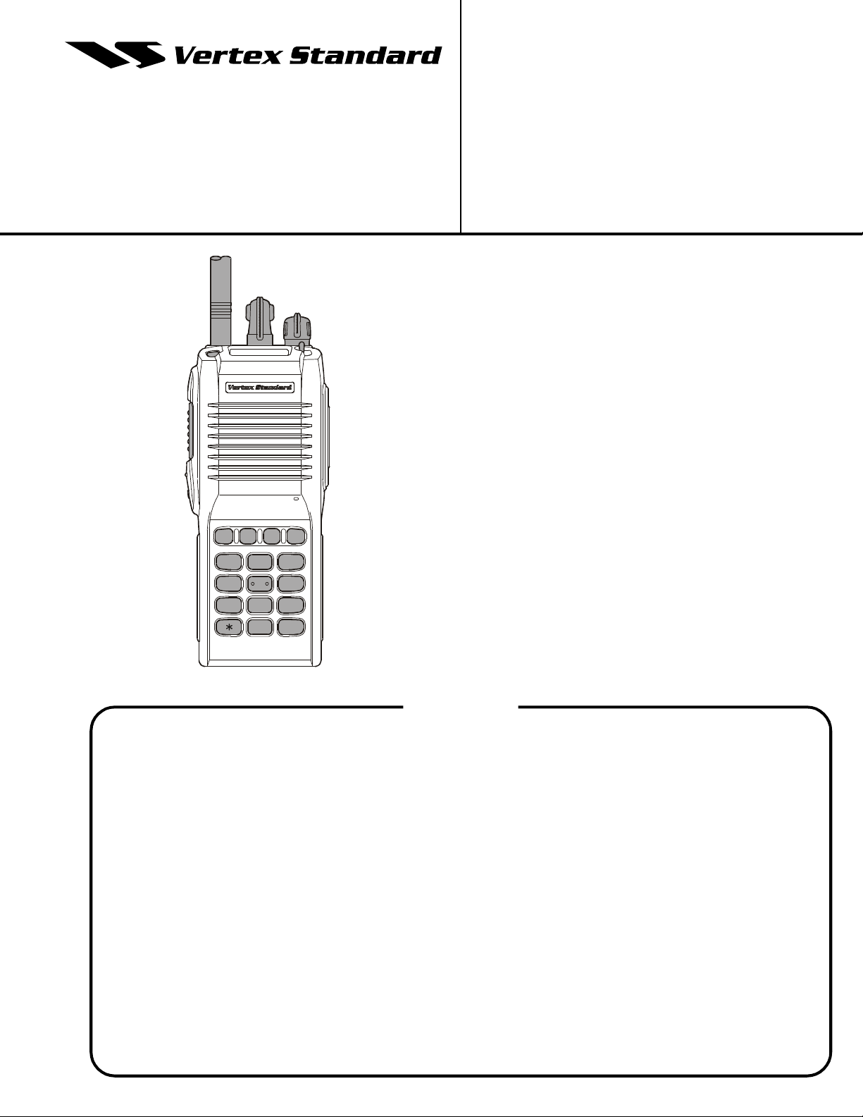
VX-900
BCD13
679
UHF Band
Service Manual
©2002 VERTEX STANDARD CO., LTD. Printed in Japan.
VERTEX STANDARD CO., LTD.
4-8-8 Nakameguro, Meguro-Ku, Tokyo 153-8644, Japan
VERTEX STANDARD
US Headquarters
10900 Walker Street, Cypress, CA 90630, U.S.A.
International Division
8350 N.W. 52nd Terrace, Suite 201, Miami, FL 33166, U.S.A.
YAESU EUROPE B.V.
P.O. Box 75525, 1118 ZN Schiphol, The Netherlands
YAESU UK LTD.
Unit 12, Sun Valley Business Park, Winnall Close
Winchester, Hampshire, SO23 0LB, U.K.
VERTEX STANDARD HK LTD.
Unit 5, 20/F., Seaview Centre, 139-141 Hoi Bun Road,
Kwun Tong, Kowloon, Hong Kong
Introduction
This manual describes the circuit theory, programming procedures, and alignment procedures for the
VX-900 UHF Portable Transceiver.
Much of the operating flexibility of the VX-900 is
derived from its versatile "Soft Key" front panel keys.
These keys may be configured for a number of operating functions, as described in this manual.
Following the discussion of transceiver operation,
details regarding programming software, alignment, and maintenance will follow.
A
2
54
8
0
#
Contents
Operating Manual Reprint ................................................................................................................................................2
Set (Menu) Mode Functions............................................................................................................................................10
Cloning................................................................................................................................................................................12
Specification.......................................................................................................................................................................13
Exploded Views & Miscellaneous Parts .......................................................................................................................14
Block Diagram ...................................................................................................................................................................15
Circuit Description ...........................................................................................................................................................17
Alignment...........................................................................................................................................................................20
Test Adapter Schematic ...................................................................................................................................................25
Board Units (Schematics, Layouts & Parts)
MAIN Unit......................................................................................................................................................................27
VR Unit ............................................................................................................................................................................ 55
SW Unit ........................................................................................................................................................................... 56
Dummy Unit .................................................................................................................................................................. 57
Optional Board Units (Schematics, Layouts & Parts)
F2D-8 2-Tone Decode Unit ........................................................................................................................................... 58
VTP-50 VX-Trunk Unit ................................................................................................................................................. 60
FVP-25 Encryption / DTMF Pager Unit ...................................................................................................................... 62
F5D-14 5-Tone Unit ....................................................................................................................................................... 64
1
Operating Manual Reprint
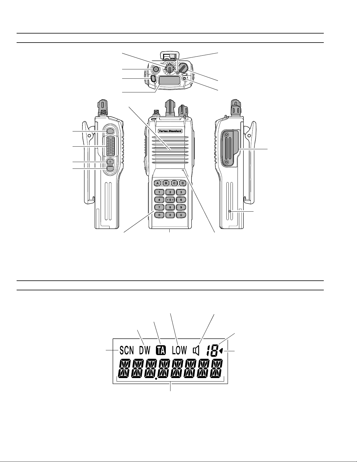
CONTROLS & CONNECTORS
LCD (Liquid Crystal Display
SIDE SEL Key
PTT Switch
MONITOR Button
LAMP Button
CH (Channel) Selector
Antenna Jack
TOP SEL Key
)
Speaker
LED Indicator
Steady Green: Signaling off
Blinking Green: Busy Channel (or SQL off)
Steady Red: Transmission in Progress
Blinking Red: Battery voltage is low
VOL/PWR Knob
TOGGLE Switch
MIC/SP Jack
(
External MIC/SP
Sub Microphone
(
Noise Canceling Microphone
)
)
16-Button DTMF Keypad
(
16-key version only
Low Transmit Power Mode On
This Channel on “DUAL WATCH” List
This Channel on “SCAN” List
)
Battery Pack Latch
LCD ICONS & INDICATORS
Talk-Around Mode
8 Charactor Alpha-numeric Invertible Display
Main Microphone
Receive Monitor
Steady On: Signal off
Blinking: Busy Channel (or SQL off)
Channel Group Number
(
“01” ~ “19” and “0”
Group Scan Enabled
(this group)
)
2
Operating Manual Reprint
BEFORE YOU BEGIN
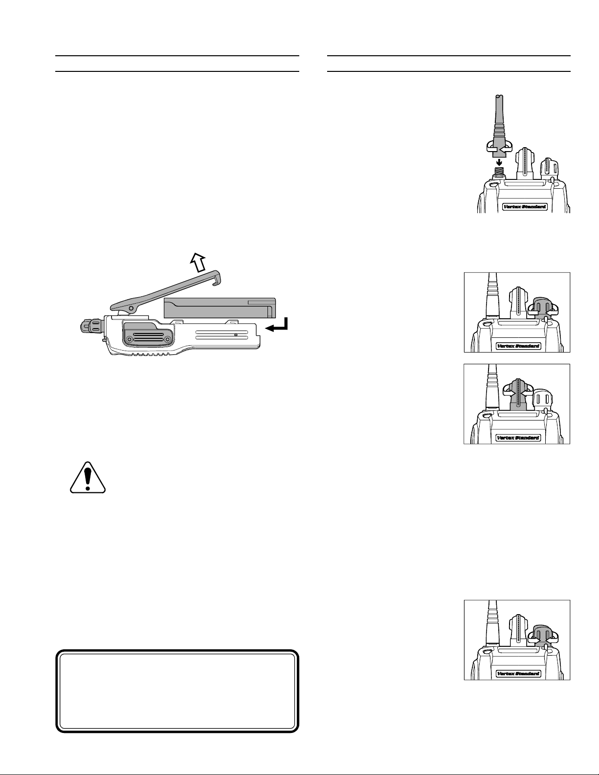
Battery Pack Installation and Removal
To install the battery, hold the transceiver with
r
your left hand, so your palm is over the speaker
and your thumb is on the top of the belt clip. Carefully mate the battery four insertion slots with
their corresponding alignment tabs on the transceiver case, while tilting the Belt Clip outward.
Proper alignment occurs with the battery pack
offset about 1/2 inch from the top edge of the battery compartment.
Guide the pack to the tabs with a slight inward
r
pressure, then slide the battery pack upward, until it locks in place with a “Click.”
Tilt the Belt Clip
OPERATION
Preliminary Steps
Install a charged battery
r
pack onto the transceiver, as
described previously.
Screw the supplied antenna
r
onto the Antenna jack.
Never attempt to operate
this transceiver without an
antenna connected.
If you have a Speaker/Mi-
r
crophone, we recommend
that it not be connected until you are familiar with
the basic operation of the VX-900.
Operation Quick Start
Turn the top panel’s VOL/
r
PWR knob clockwise to
turn on the radio on.
Insert the Battery Pack
To remove the battery, turn the radio off and re-
r
move any protective cases. Slide the Battery Pack
Latch on the bottom of the radio toward the front
panel while sliding the battery down about 1/2
inch. Then lift the battery out from the radio while
unfolding the Belt Clip.
Do not attempt to open any of the rechargeable Lithium-Ion pack, as they
could explode if accidentally short-cir-
cuited.
Low Battery Indication
As the battery discharges during use, the voltage
gradually becomes lower. When the battery voltage
reaches 6.0 volts, it is time to substitute a freshly
charged battery and recharge the depleted pack. The
LED indicator on the top of the radio will blink red
when the battery voltage is low (6 Volts or lower).
CAUTION
Danger of explosion if battery is incorrectly
replaced.
Replace only with the same or equivalent type.
Turn the top panel’s CH
r
selector knob to choose
the desired operating
channel. A channel name
will appear on the LCD. If
you want to select the operating channel from a
different Memory Channel Group, pressing the
Soft key (assigned to the Memory Group Up or
Down function) to select the Memory Channel
Group to be you want before selecting the operating channel. A group name will appear on the LCD
whenever the Soft key is pressed.
Note: Some models are programmed so that the
operating channels are selected by the Soft key
and the memory channel group is selected by the
channe selector knob. For further details, contact
your VERTEX STANDARD dealer.
Rotate the VOL/PWR
r
knob to set the volume
level. If no signal is
present, press and hold
in the MONITOR button
(under the PTT switch)
more than 2 seconds;
background noise will now be heard, and you
may use this to set the VOL/PWR knob for the
desired audio level. Press and hold the MONITOR
button more than 2 seconds (or press the MONI-
3
Operating Manual Reprint
TOR button twice) to
quiet the noise and resume normal (quiet)
monitoring.
To transmit, press and
r
hold the PTT switch.
Speak into the microphone area of the front
panel grille (above the
[D]
key) in a normal voice
level. To return to the Receive mode, release the PTT switch.
Press the Soft key (if assigned to the Scan func-
r
tion) or switch the TOGGLE Switch to the assigned “Scan” position (when so programmed by
your dealer) to start the scanner. The scanner rapidly steps through each of the dealer-programmed channels, looking for incoming calls.
Press the TOP SEL key
r
(on the top panel) or
SIDE SEL key (the top
button on the left side) to
activate one of the
preprogrammed functions which may have
been enabled at the time
of programming by the
dealer. Similarly, when
using the 16-key version,
the [A], [B], [C], and [D
function keys activate
one of these functions, if
programmed by the dealer. See the next section
for details regarding the available features.
]
r Switch the top panel’s
TOGGLE switch to the
[A], [B] or [Center] position to activate one of the
pre-programmed functions which may have
been enabled at the time
of programming by the dealer. When this switch
is in the [A (left)], [B (right)] or [Center] position,
the feature programmed (by your dealer) to that
switch position will be activated. See the next section for details regarding the available features.
r Press the DTMF keys on the telephone keypad
while pressing the PTT switch to send DTMF
tones (16-key version only).
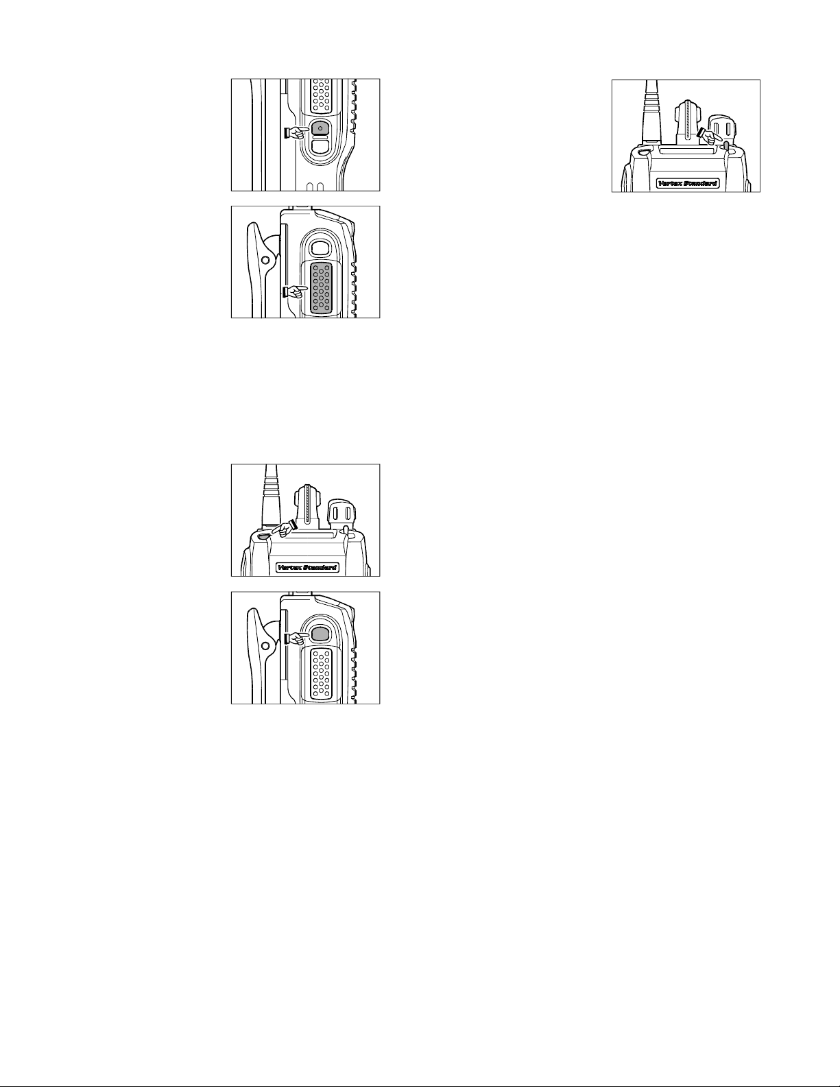
r If a Speaker/Microphone is available, remove the
plastic cap and its two mounting screws from the
right side of the transceiver, then align the connector of the Speaker/Microphone on the transceiver body; secure the connector pin using the
screws supplied with the Speaker/Microphone.
Hold the speaker grille up next to your ear while
receiving. To transmit, press the PTT switch on
the Speaker/Microphone, just as you would on
the main transceiver’s body, and speak into the
microphone on a normal voice level.
Note: Save the original plastic cap and its mounting screws. They should be reinstalled when not
using the Speaker/Microphone.
4
Operating Manual Reprint
ADVANCED OPERATION
Soft key and TOGGLE switch Functions
The VX-900 includes the [TOP SEL], [SIDE SEL],
[
MONITOR], and [LAMP] keys, and the TOGGLE
switch, while the 16-key version additionally provides [A], [B], [C], [D] function keys. The Soft key
and TOGGLE switch functions can be customized,
via programming by your VERTEX STANDARD
dealer, to meet your communications/network requirements. Some features may require the purchase
and installation of optional internal accessories. The
possible Soft key and TOGGLE switch programming features are illustrated at the right, and their
functions are explained on next page. For further
details, contact your VERTEX STANDARD dealer.
For future reference, check the box next to each function that has been assigned to the Soft key and TOG-
GLE switch on your particular radio, and keep it
handy.
Functions
None
Channel Scan
Dual Watch
High/Low Power
Talk Around
TX Save Disable
LCD Invert
Encryption Disable
Follow-Me DW
Call/Reset
Speed Dial
Emergency
Group Up
Group Down
Channel Up
Channel Down
Monitor
Lamp
ø
ø
TOP SEL
SIDE SEL MONITOR LAMP
Functions
None
Channel Scan
Dual Watch
High/Low Power
Talk Around
TX Save Disable
LCD Invert
Encryption Disable
Lock
Follow-Me Scan
Group recall Shortcut
:
Requires FVP-25 DTMF/Encryption Unit
ø
Soft key
[A] [B] [C] [D]
ø
TOGGLE switch (Position
A B
center
£ Group 1
£ Group 2
£ Group 3
£ Group 1
£ Group 2
£ Group 3
£ Group 1
£ Group 2
£ Group 3
)
:
Requires FVP-25 DTMF/Encryption Unit
ø
5

Operating Manual Reprint
ADVANCED OPERATION
Description of Operating Functions
Channel Scan
The Scanning feature is used to monitor multiple signals programmed into the transceiver. While scanning,
the transceiver will check each channel for the presence of a signal, and will stop on a channel if a signal
is present.
One key or switch may be assigned to the Scan function, as follows:
One of the Soft keys may be assigned for Scan
r
operation; or
The TOGGLE switch may have one position as-
r
signed to the Scan function.
To activate scanning:
Press the assigned Soft key, or set the TOGGLE
¦
switch to the assigned position.
The scanner will search the channels, looking for
¦
active ones; it will pause each time it finds a channel on which someone is speaking.
To stop scanning:
Press the assigned Soft key, or set the TOGGLE
¦
switch to a different position.
Operation will revert to the channel to which the
¦
CH knob is set.
Note: Your dealer may have programmed your radio
to stay on one of the following channels if you press
the PTT switch during scanning pause:
Current channel (“Talk Back”)
£
“Last Busy” channel
£
“Priority” channel
£
“Home” channel
£
“Scan Start” channel
£
Dual Watch
The Dual Watch feature is similar to the Scan feature,
except that only two channels are monitored:
r The current operating channel; and
r The “Priority” channel.
To activate Dual Watch:
Press the assigned Soft key, or set the TOGGLE
¦
switch to the assigned position.
The scanner will search the two channels; it will
¦
pause each time it finds a channel on which someone is speaking.
To stop Dual Watch:
Press the assigned Soft key, or set the TOGGLE
¦
switch to a different position.
Operation will revert to the channel to which the
¦
CH knob is set.
High/Low Power
Press the assigned Soft key or switch the Toggle
switch to the assigned position to set the radio’s transmitter to the “Low Power” mode, thus extending battery life. Press the assigned Soft key again or switch
the TOGGLE switch to the other Position to return to
“High Power” operation when in difficult terrain.
Talk Around
Press the assigned Soft key or switch the TOGGLE
switch to the assigned position to activate the Talk
Around feature when you are operating on duplex channel systems (separate receive and transmit frequencies,
utilizing a “repeater” station). The Talk Around feature allows you to bypass the repeater station and talk
directly to a station that is nearby. This feature has no
effect when you are operating on “simplex” channels,
where the receive and transmit frequencies are already
the same.
Note that your dealer may have made provision for
“Talk Around” channels by programming “repeater”
and “Talk Around” frequencies on two adjacent channels. If so, the key may be used for one of the other
Pre-Programmed Functions.
TX Save Disable
Press the assigned Soft key or switch the TOGGLE
Switch to the assigned position to disable the Transmit
Battery Saver, if you are operating in a location where
high power is almost always needed.
The Transmit Battery Saver helps extend battery life
by reducing transmit power when a very strong signal
from an apparently nearby station is being received.
Under some circumstances, though, your hand-held
radio may not be heard well at the other end of the
communication path, and high power may be necessary at all times.
LCD Invert
Press the assigned Soft key or switch the TOGGLE
switch to the assigned position inverts the LCD display to backward-facing readout (the backward display is convenient for viewing when wearing the transceiver on your belt). Press the assigned Soft key again
or switch the TOGGLE switch to the other Positionreturn the LCD display to frontward-facing readout.
Encryption Disable
Press the assigned Soft key or switch the TOGGLE
switch to the assigned position to turn off the optional
voice encryption unit temporarily, for use when an incorrect setting of (or failure in) the encryption system
at one end of the communication path has made it im-
6

Operating Manual Reprint
ADVANCED OPERATION
possible to talk to the other station.
Remember that disabling the encryption will mean that
your transmissions are no longer secure. Return to the
encrypted mode as soon as possible, and do not discuss
any critical or confidential information while in the non-
encrypted mode of operation.
Lock
Switch the TOGGLE switch to lock the top-panel keys;
this can be enabled to prevent radio settings from be-
ing disturbed.
Follow-Me Scan
“Follow-Me” Scan feature checks a User-assigned Pri-
ority Channel regularly as you scan the other chan-
nels. Thus, if only Channels 1, 3, and 5 (of the 8 avail-
able channels) are designated for “Scanning,” the user
may nonetheless assign Channel 2 as the “User-as-
signed” Priority Channel via the “Follow-Me” feature.
To activate “Follow-Me” scanning, first select the chan-
nel you want to designate as the “User-Assigned Pri-
ority Channel” and Switch the TOGGLE switch to
the assigned position. Then turn the CH selector knob
to the “Scanning Start” channel which has been pro-
grammed by your dealer to activate the scanner. When
the scanner stops on an “Active” channel, the User-
assigned Priority Channel will automatically be
checked every few seconds; if activity is found on the
User-assigned Priority Channel, the radio will switch
between it and the Dealer-Assigned Priority Channel,
if any.
Follow-Me DW
To set up a “Dual Watch” frequency pair using the “Fol-
low-Me” feature, select a channel using the CH selector
knob. Now press the assigned Soft key; pressing the as-
signed Soft key locks the current channel as the User-
assigned Priority Channel. Now rotate the CH selector
knob to another channel (not the “Scanning Start” chan-
nel). Your radio will now switch back-and-forth between
the currently-selected channel (shown on the CH selec-
tor knob) and the User-assigned Priority Channel.
During “Follow-Me” scanning (after you have pressed
the key), you can set up the “Dual Watch” feature by
rotating the CH selector knob to another channel. The
radio will then scan back and forth between the origi-
nal User-assigned Priority Channel and the newly-se-
lected channel.
The Priority Channel you have assigned (before press-
ing the key) will be retained in memory until you
change it.
Channel Group Selection
The VX-900 is capable of separating its 512 memory
channels into any of 20 Groups. There is no limit as to
the number of channels which may be assigned to each
Group. The Dealer will have made the Group assignment at the time of channel programming. At the same
time, one of the Soft Keys will be assigned as the
Channel Group Selection key.
To change Channel Groups, press the assigned
soft key to step through the available Groups. Once
the desired Group is reached, rotate the CH selector
knob to select the desired channel within the selected
Group.
You may wish to have the Scanner (described previously) pass through more than one Group during the
scanning process (normally, scanning is performed
within the current group only). To include the current
Group in the scanning loop, press and hold in the assigned Soft key for one second.
To remove a Group from Group Scan, press and
hold in the assigned Soft key again for one second.
Multi-Group Scanning is only possible if you are using the “User Scan” list.
The VX-900 has two scanning “lists:” the “Dealer
Scan” list and the “User Scan” list. The “Dealer Scan”
list is a fixed group of stations which will be included
when scanning is activated. The “User Scan” list is a
different list, initially arranged by the Dealer, which
may be modified by the User (if, for example, you want
to delete one or more of these channels from the scanning list).
To edit the User Scan list, press and hold the soft
key (assigned to the Group Up/Down function) to delete the current Memory Group from the Scanning.
Alternatively, press and hold the “Scan” Soft key for
one second to delete the Current Memory channel from
the Scanning.
When you delete a Group or channel, “-SKIP-” will
appear on the LCD for one second after press ing the
Soft key. To restore a particular channel to your scanning list, press and hold in the Soft key again for one
second; “-STOP-” will appear on the LCD for one second after pressing the Soft key.
Call/Reset
This feature, if enabled, allows the user to change the
3-digit Page Call code, used to call other similarlyequipped stations. Press the Dealer-assigned soft key,
followed by the three digits representing the Page Call
code of the station you wish to call. Three tones will
7

Operating Manual Reprint
ADVANCED OPERATION
be heard after the last key is pressed (the new code
will now be transmitted).
The receiver squelch of the other station will be opened,
and you can begin communication.
Speed Dial
Your Dealer may have pre-programmed Auto-Dial telephone number memories into your radio.
To dial a number, press the Dealer-assigned Soft key
for Speed Dialing, then press the numbered key corresponding to the Auto-Dial memory number list provided by your Dealer. The DTMF tones sent during
the dialing sequence will be heard in the speaker.
Emergency
The VX-900 includes an “Emergency” feature which
may be useful if you have someone monitoring on the
same frequency as your transceiver’s channel. For further details contact your nearest VERTEX STAN-
DARD dealer.
ARTS (Auto Range Transpond System)
This system is designed to inform you when you and
another ARTS-equipped station are within communication range.
During ARTS operation, your radio automatically
transmits for about 1 second every 25 seconds (the
interval is programmed by the Dealer) in an attempt
to shake hands with the other station.
If you move out of range for more than two minutes, your radio senses that no signal has been received, a ringing beeper will sound, and "OUT OF
SERVICE" will scroll on the LCD. If you subsequently move back into range, as soon as the other
station transmits, your beeper will sound, and "IN
SERVICE" will scroll on the LCD.
DTMF Paging System
This system allows paging and selective calling, using DTMF tone sequences.
When your radio is paged by a station bearing a tone
sequence which matches yours, your radio's squelch
will open and the alert ringer will sound (unless you
have disabled it, as described previously).
The three-digit code of the station which paged you
will be displayed on your radio's LCD.
8

Operating Manual Reprint
ACCESSORIES & OPTIONS
FVP-25 Encryption/DTMF Pager Unit
F2D-8 2-Tone Decode Unit
F5D-14 5-Tone ENC/DEC Unit
FNB-V68LI 7.4 V 1800 mAh Lithium-Ion Battery
FNB-V69LI 7.4 V 2400 mAh Lithium-Ion Battery
FBA-27 Alkaline Battery Case (6 x AA)
VAC-900 Rapid Desktop Charger
VAC-6900 6-Unit Multi Charger
VCM-1 Mobile Mounting Bracket
VTP-50 VX-Trunk Unit
MH-50
VH-110 Over the Head, Heavy Duty Headset
VH-120 3 wire Mini Lapel Microphone
A7A
Availability of accessories may vary; some accessories are supplied standard per local requirements, others may be
unavailable in some regions. Check with your VERTEX STANDARD Dealer for changes to the this list.
Speaker/Microphone (Noise Canceling)
VH-130 Surveillance Kit (Palm Mic/Earpiece)
VH-140 DSP VOX Earpiece Microphone
VH-150 DSP VOX Headset
VH-170 Bone Knocker Headset
CE39 Programing Software
CT-70 Radio Programing Cable (Requires VPL-1)
CT-71 PC Programing Cable
CT-72 Radio to Radio Programming Cable
LCC-900 Leather Case
ATU-6A UHF Antenna, 400 ~ 430 MHz
ATU-6C UHF Antenna, 440 ~ 470 MHz
ATU-6D UHF Antenna, 450 ~ 485 MHz
9

Set (Menu) Mode Functions
One or more of the radio’s "Soft Keys" may be enabled for a function associated with the "Set" (Menu)
mode. This feature, when activated, allows the user
to customize certain performance aspects of the VX-
900. Note that some of these items may also appear
as available "Soft Keys," described below.
The operating procedure for the Menu mode is quite
simple, requiring only a few easily- remembered
actions on the user’s part.
The VX-900 Soft Keys include the [TOP SEL], [SIDE
SEL], [MON], and [LAMP] Keys, plus the [A], [B],
[C], and [D] keys on the 16-key version. The Soft Key
functions can be assigned either as a "Menu" function or an "operating" function at the time of programming.
Basic Menu Mode Operation
1. Press the appropriate Soft Key to activate a Menu
function. The available keys include the [TOP
SEL], [SIDE SEL], [MON], and [LAMP] Keys, plus
the [A], [B], [C], and [D] keys on the 16-key ver-
sion.
2. Rotate the top panel’s CH selector knob to select
the feature you wish to view and/or modify.
3. Press the [TOP SEL] and/or [SIDE SEL] keys to
modify or adjust the current setting of this Menu
item ("On" to "Off," etc.)
4. Rotate the CH selector to save the new setting.
5. Press the PTT switch to exit the Set (Menu) mode.
No.2 LIST (Scanning List)
The VX-900 has two scanning "lists:" the "Dealer
Scan" list and the "User Scan" list. The "Dealer scan"
list is a fixed group of stations which will be included
when scanning is activated. The "User Scan" list is a
different list, initially arranged by the dealer, which
may be changed by the User.
This Menu item allows you to select the desired scanning list: "Dealer Scan" or "User Scan".
After selecting this Menu item, press the [TOP SEL]
or [SIDE SEL] key to select the Scan List in which
you wish to scan ("LIST DLR: Dealer List" or "LIST
USR: User List"). Rotate the CH selector knob to save
the new setting, then press the PTT switch to exit
the Set (Menu) mode.
No.3 BEEP (Keypad Beeper On/Off)
After selecting this Menu item, press the [TOP SEL]
or [SIDE SEL] key to enable (ON) or disable (OFF)
the keypad beep tones. Rotate the CH selector knob
to save the new setting, then press the PTT switch
to exit the Set (Menu) mode.
No.4 BELL (CTCSS/DCS/Paging Alert Bell On/Off)
After selecting this Menu item, press the [TOP SEL]
or [SIDE SEL] key to enable (ON) or disable (OFF)
the alert bell which sounds when your radio is called
using either CTCSS or DCS calling tones. Rotate the
CH selector knob to save the new setting, then press
the PTT switch to exit the Set (Menu) mode.
Available Soft Key Menu Functions
No.1 SQL (Squelch Level)
After selecting this Menu item, press the [TOP SEL]
or [SIDE SEL] key to find the point where the background noise is just silenced. This is the point of best
receiver sensitivity consistent with quiet monitoring. The scale for the Squelch Level adjustment is 0
~ 11 and 12 (RSSI SQL), The default value is 8.
When the Squelch Level set to "12," this activates
the RSSI (Received Signal Strength Indicator)
Squelch feature, which allows you to set the squelch
so that only signals exceeding a prescribed RX signal input level will open the squelch. The RX signal
input level is determined via the Alignment Program
SVC39. See page 22 for details regarding the RSSI
level setting.
10
No.5 LGT (TX/BUSY LED On/Off)
After selecting this Menu item, press the [TOP SEL]
or [SIDE SEL] key to enable (ON) or disable (OFF)
the LED which serves as the Busy Channel and
Transmitter On indicator. Turning this LED off will
extend battery life somewhat. Rotate the CH selector knob to save the new setting, then press the PTT
switch to exit the Set (Menu) mode.
No.6 LOCK (Keypad, PTT, or Knob Disabling)
In some situations, you may wish to disable the keypad's keys, the CH selector knob, and/or the PTT
switch (so as to prevent transmission by unauthorized users of the radio). The LOCK Menu item determines which features will be disabled when the
LOCK function is engaged.
After selecting this Menu, press the [TOP SEL] or

Set (Menu) Mode Functions
[SIDE SEL] key to select "P" (PTT Lock), "D" (DialKnob-Lock), "K" (Keypad Lock), or various combinations of these. Rotate the CH selector knob to save
the new setting, then press the PTT switch to exit
the Set (Menu) mode.
No.7 GROUP (Group Select)
This Menu item allows you to change Channel
Groups, in the event that a Soft Key has not been
designated for this purpose. After selecting this
Menu, press the [TOP SEL] or [SIDE SEL] key to
select the Channel Group in which you wish to operate. Rotate the CH selector knob to save the new
setting, then press the PTT switch to exit the Set
(Menu) mode.
No.8 SCAN (Scan Mode On/Off)
This Menu item allows you to start the scanner, in
the event that a Soft Key has not been designated
for this purpose.
After selecting this Menu item, press the [TOP SEL]
or [SIDE SEL] key to start ("SCAN ON") or stop
("SCAN OFF") the scanner. Rotate the CH selector
knob to save the new setting, then press the PTT
switch to exit the Set (Menu) mode.
No.9 DW (Dual Watch On/Off)
This Menu item allows you to activate the Dual
Watch feature, in the event that a Soft Key has not
been designated for this purpose.
After selecting this Menu item, press the [TOP SEL]
or [SIDE SEL] key to enable ("DW ON") or disable
("DW OFF") the Dual Watch feature. Rotate the CH
selector knob to save the new setting, then press the
PTT switch to exit the Set (Menu) mode.
No.10 TA (Talk Around)
This Menu Item allows you to activate the Talk
Around feature, in the event that a Soft Key has not
been designated for this purpose. Talk-Around allows direct simplex communications between portables and/or mobiles, utilizing the repeater's downlink frequency.
After selecting this Menu item, press the [TOP SEL]
or [SIDE SEL] key to enable ("TA ON") or disable
("TA OFF") the Talk Around feature. Rotate the CH
selector knob to save the new setting, then press the
PTT switch to exit the Set (Menu) mode.
No.11 ENCR (Encryption)
On channels where scrambling is used, an incorrect
setting of (or failure in) the encryption system at one
end of the communication path will make it impossible to talk to the other station. To change the current status of encryption on your radio, after selecting this item, press the [TOP SEL] or [SIDE SEL]
key to enable (ENCR EN) or disable (ENCR DI) encryption. Rotate the CH selector knob to save the
new setting, then press the PTT switch to exit the
Set (Menu) mode.
Remember that disabling encryption will mean that
your transmissions are no longer secure.
Return to the encrypted mode as soon as possible, and do
not discuss any critical or confidential information while
in the non- encrypted mode of operation.
No.12 AF VR
This Menu item determines the audio volume level
when the top panel's VOL knob is set to its fully counterclockwise position (but not into the click stop).
This permits the programming of a certain minimum
audio output level, in applications where the radio
should never go totally silent.
After selecting this item, press the [TOP SEL] or
[SIDE SEL] key to select the desired (minimum)
volume level. Rotate the CH selector knob to save
the new setting, then press the PTT switch to exit
the Set (Menu) mode.
No.13 BP VR (Beep VR)
This Menu item determines the beep volume level.
After selecting this item, press the [TOP SEL] or
[SIDE SEL] key to select the desired level. Rotate
the CH selector knob to save the new setting, then
press the PTT switch to exit the Set (Menu) mode.
11
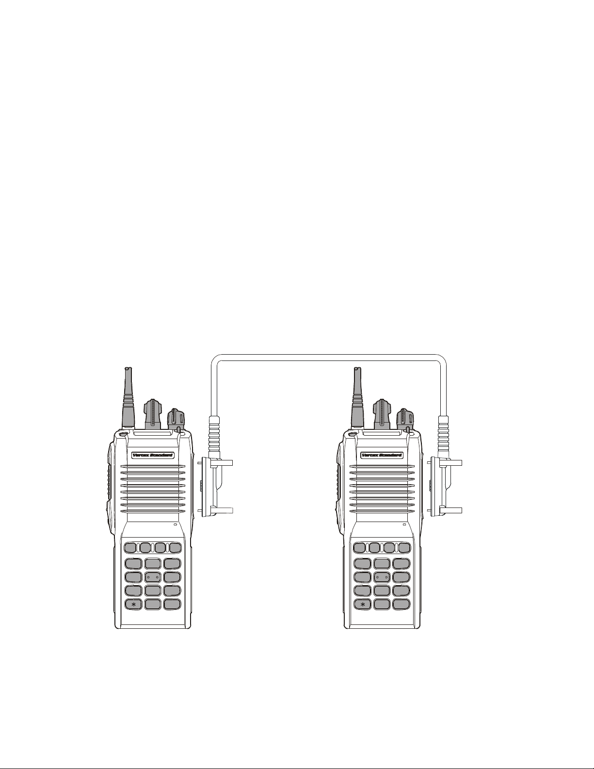
Cloning
ABCD1328054679#
The VX-900 includes a convenient “Clone” feature,
which allows the programming data from one transceiver to be transferred to another VX-900. Here is
the procedure for Cloning one radio’s data to another.
1. Turn both transceivers off.
2. Remove the plastic cap and its two mounting
screws from the MIC/SP jack on the right side of
the transceiver. Do this for both transceivers.
3. Connect the optional CT-72 cloning cable between the MIC/SP jacks of the two transceivers.
4. Press and hold the PTT and Monitor (just below
the PTT) switches while turning the transceiver
on. Do this for both transceivers (the order of the
switch-on does not matter). “CLONE” will appear on the displays of both transceivers when
Clone mode is successfully activated in this step.
5. On the Destination transceiver, press the Moni-
tor switch (“LOADING” will appear on the LCD).
6. Press the PTT switch on the Source transceiver;
“SENDING” will appear on the Source transceiver, and the data transferred.
7. If there is a problem during the cloning process,
“ERR” will be displayed. Check your cable connections and battery voltage, and try again.
8. If the data transfer is successful, the display return to “CLONE”. Turn both transceivers off and
disconnect the CT-72. You can then turn the transceivers back on, and begin normal operation.
9. Replace the plastic cap and its two mounting
screws.
Optional Cloning Cable CT-72
A B C D
1 32
54 6
7 9
8
0
#
12

Specifications
GENERAL
Number of Channels: 512 channels
Frequency Range: 400 - 430 MHz (AS1), 440 - 470 MHz (CS), 450 - 485 MHz (D), 485 - 512 MHz (F)
Channel Spacing: 12.5 / 20 / 25 kHz
PLL Steps: 5 / 6.25 kHz
Power Supply Voltage: 7.4 VDC ± 20 %
Battery Life (5-5-90 duty): w/ FNB-V68LI (1800 mAh): 11 hrs. (14 hrs. w/ saver) @5 W
w/ FNB-V69LI (2400 mAh): 14 hrs. (18 hrs. w/ saver) @5 W
Temperature Range: –22°F to +140°F (–30°C to +60°C)
Frequency Stability: EIA: ±2.5 ppm
ETS: ±1.5 kHz
Case Size: 2.3" (w) x 6.1" (H)x 1.3" (D) (59 x 155 x 34 mm) w/ FNB-V68LI
Weight (approx.): 0.93 lb. (420 g) w/Antenna, FNB-V68LI and Belt clip
Battery: Lithium-Ion 7.4 V 1800 mAh / Lithium-Ion 7.4 V 2400 mAh (optional)
RECEIVER
Circuit Type: Double-conversion Super-heterodyne
Sensitivity: EIA12-dB SINAD: 0.25 µV
20 dB Quieting: 0.7 µV (emf)
ETS (20 dB SINAD: 0.5 µV (emf)
Adjacent Channel Selectivity: EIA: 75 dB (25 kHz) / 68 dB (12.5 kHz)
ETS: 70 dB (25 kHz) / 60 dB (12.5 kHz)
Intermodulation: EIA: 75 dB (25 kHz) / 65 dB (12.5 kHz)
ETS: 65 dB (25 kHz / 12.5 kHz)
Spurious and Image Rejection: EIA: 75 dB
ETS: 70 dB
Hum & Noise: EIA: 45 dB
ETS: 45 dB
AF Output: 700 mW @ 16 Ohms, 5% THD
TRANSMITTER
Power Output: 5.0 / 2.5 / 1.0 / 0.25 W (selectable)
Modulation System: EIA: Direct FM 16K0F3E, 11K0F3E
ETS: 16K0G3E, 8K50G3E
Conducted Spurious Emissions: EIA: 70 dB Below Carrier
ETS: 73 dB Below Carrier
FM Hum & Noise: 45 dB (25 kHz) / 40 dB (12.5 kHz)
Audio Distortion (@ 1 kHz): < 3 %
Measuremente per EIA/ETS standards unless noted adove.
Specifications subject to change without notice or obligation.
13
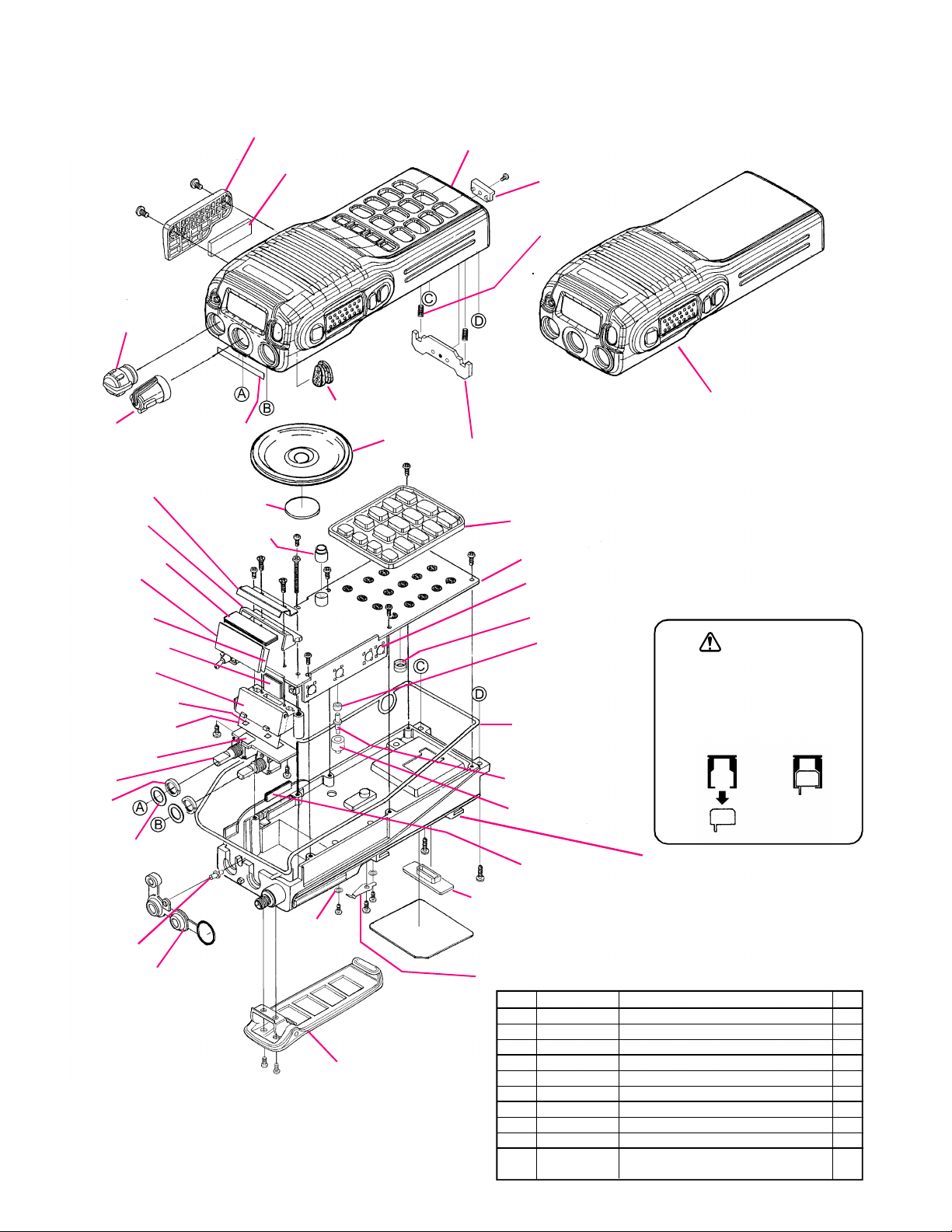
Exploded View & Miscellaneous Parts
Ç
RA030720A (Lot. 2~)
RA0307200 (Lot. 1~)
KNOB
RA030770B (Lot. 4~)
RA030770A (Lot. 1~)
KNOB
RA0296900
HOLDER PLATE
RA0296600
BRACKET
RA0298200
INTER CONNECTOR
G6090144
LCD
RA0317800
DIFFUSER SHEET
RA0298300
INTER CONNECTOR
RA0296500
LIGHT GUIDE
RA0316600 (x2 pcs)
REFLECTOR SHEET A
RA0316700
REFLECTOR SHEET B
RA0317200
LIGHT SHEET A
VR UNIT
R6147510
(x2 pcs)
RING NUT
RA0318200 (x2 pcs)
WASHER (B)
RA0297700
LIGHT GUIDE
RA029800A (Lot. 2~)
RA0298000 (Lot. 1~)
RUBBER PACKING
LIGHT SHEET B
Non-designated parts are available only as
part of a designated assembly.
Ç
RA0317300
RA0317000
SHEET (SP)
RA0207800
MIC HOLDER*
Á
RA0297600
EXT CAP
Ã
Â
Ã
Á
È
RA0215400
SHEET
RUBBER KNOB
Â
Â
Ä
Â
RA0299400
(x2 pcs)
WASHER
È
BELT CLIP ASS'Y
RA0297500
M4090153
SPEAKER
Â
Æ
Æ
Å
CP6955001
RA029850B (Lot. 3~)
RA029850A (Lot. 1~)
FRONT CASE ASS'Y (16KEY)
À
RA0297300
RA0306900 (x2 pcs)
COIL SPRING
RA0297000
LATCH PLATE
Â
RA0295300
RUBBER KNOB
Â
MAIN UNIT
SW UNIT
RA0140200
MIC HOLDER
RA0305100
HOLDER (+)
RA0350400 (Lot. 8~)
RA029680A (Lot. 2~)
RA0296800 (Lot. 1~)
RUBBER PACKING
RA0120500
SPRING CONNECTOR
RA0298100
RUBBER HOLDER (+)
É
É
DUMMY UNIT
RA0239100
INTER CONNECTOR
RA029720A (Lot. 3~)
RA0297200 (Lot. 1~)
TERMINAL PLATE (-)
REF. VXSTD P/N Description Qty.
À U07230107 PAN HEAD SCREW M2X3B #1 1
Á U9900094 TAPTITE SCREW M2X5NI#2 2
 U44104002 TAPTITE SCREW M2X4NI 7
à U9900116 TAPTITE SCREW M2X8NI #2 2
Ä U00119006 PAN HEAD SCREW M2X18AU 1
Å U9900117 TAPTITE SCREW M2X4NI #2 1
Æ U07240202 PAN HEAD SCREW M2X4NI#2 2
Ç U20305007 BINDING HEAD SCREW M3X5B 2
È U02206007 SEMS SCREW SM2.6X6B 2
U20206002 BINDING HEAD SCREW M2.6X6NI 2
É
U24208002
HOOK
RA029860B (Lot. 3~)
RA029860A (Lot. 1~)
FRONT CASE ASS'Y (KEYLESS)
*
CAUTION
The mic element must be desoldered and removed from the PCB
on order to reinstall its protective
rubber cover.
Therefore, be careful not to remove this cover unless mic element replacement is necessary.
À
CP6954001
REAR CASE ASS'Y
(with/ MIC CONNECTOR,
DOUBLE FACE,
SMA CONNECTOR,
COVER,
SHEET (MICROTEX 5.6X3),
RUBBER PACKING )
TAPTITE SCREW M2.6X8NI (Lot. 3~)
Á
2
14
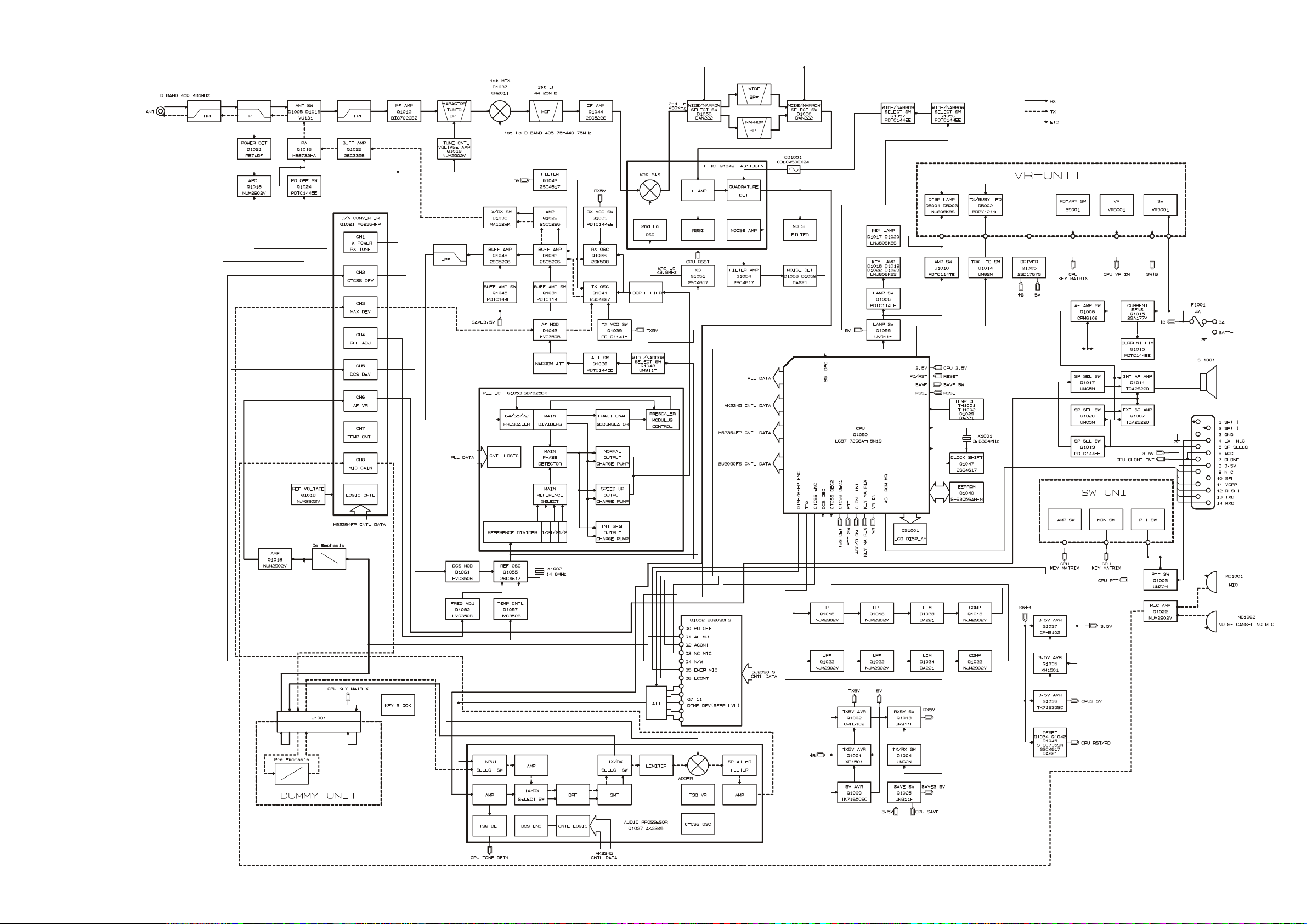
Block Diagram
15

Block Diagram
Note:
16

Circuit Description
Overview
The VX-900 is a UHF FM hand-held transceiver designed to operate in the frequency range of 400 to
512 MHz.
Circuit Configuration by Frequency
The receiver is a double-conversion superheterodyne with a first intermediate frequency (IF) of 44.25
MHz and a second IF of 450 kHz. Incoming signals
from the antenna are mixed with the local signal
from PLL to produce the first IF of 44.25 MHz.
This is then mixed with the 43.8 MHz second local
oscillator (using the 14.6 MHz reference crystal) output to produce the 450 kHz second IF. This is subsequently detected to produce the demodulated signal.
The transmit signal frequency is directly generated
by the PLL VCO, and modulated by the signal from
the microphone. It is then amplified and sent to the
antenna.
Receive Signal Path
Front-end RF Amplifier
Incoming RF from the antenna jack is delivered to
the RF Unit and passes through a low-pass filter and
high-pass filter consisting of coils L1002, L1003,
L1005, L1007, L1001, L1004, L1006, L1008, L1009
and L1011, capacitors C1002, C1005, C1009, C1011,
C1019, C1028, C1003, C1012, C1015, C1018, C1022,
C1026, C1030, C1035, C1036, C1039 and C1042, and
antenna switching diode D1016 (HVU131).
Signals within the frequency range of the transceiver
are then amplified by Q1012 (BIC702C) and enter a
varactor-tuned band-pass filter consisting of coils
L1014, L1015, and L1017, capacitors C1081, C1083,
C1094, C1097, C1105, C1106, C1115, C1117, C1121,
C1123, C1134, C1139, and C1145, resisters R1079,
R1106 and R1124, and diodes D1027, D1028, D1030,
D1031, D1032, and D1033 (all HVC350) before de-
livery of the RF signal to the first mixer.
First Mixer
Buffered output from the VCO is amplified by Q1029
(2SC5226-4/5) to provide a pure first local signal between 355.75 and 467 MHz for injection to the first
mixer D1037 (GN2011-Q). The 44.25 MHz first mixer
product then passes through monolithic crystal fil-
ters XF1001 and XF1002 (MDF0028, ±5.5 kHz BW)
to strip away all undesired mixer products.
IF Amplifier
The first IF signal is amplified by Q1044 (2SC52264/5).
The amplified first IF signal is applied to FM IF subsystem IC Q1049 (TA31136FN), which contains the
second mixer, second local oscillator, limiter amplifier, noise amplifier, and S-meter amplifier.
A second local signal is generated by Q1051
(2SC4617) using the 14.6 MHz crystal X1002 as a
reference, producing a 43.8 MHz signal; this which
yields a 450 kHz second IF when the reference signal is mixed with the first IF signal within Q1046.
The second IF then passes through the ceramic filter CF1001 (PBFC450R15D: wide channels),
CF1002 (PBFC450R9DR: narrow channels) to strip
away all but the desired signal, and is applied to the
limiter amplifier in Q1049, which removes amplitude variations in the 450kHz IF, before detection of
the speech by the ceramic discriminator CD1001
(CDBC450CX24).
Audio Amplifier
Detected audio from Q1049 is applied to
Q1027(AK2345) and the audio low-pass filter, and
then through the volume control (Q1021:M62364FP)
to the audio amplifier Q1007 (TDA2822D;external
speaker) or Q1011 (TDA2822D;internal speaker), pro-
viding up to 0.5 Watt to the optional headphone jack
or 16-ohm loudspeaker.
Attention: Audio output is BTL output. Both sides
of the audio output are above ground, and this line
must not be connected to a speaker line which uses
a grounded shield.
Squelch Control
The squelch circuitry consists of a noise amplifier
and band-pass filter within Q1049, and noise detector D1058/D1059 (DA221).
When no carrier received, noise at the output of the
detector stage in Q1049 is amplified and band-pass
filtered by the noise amplifier section of Q1049 and
the network between pins 7 and 8, and then rectified by D1058.
17

Circuit Description
The resulting DC squelch control voltage is passed
to pin 19 of the microprocessor Q1050. If no carrier
is received, this signal causes pin 6 of Q1052
(BU2090FS) to go low and pin 89 of Q1050 to go
high. Pin 6 of Q1052 signals Q1008 (CPH6102),
Q1017 (UMC5N) and Q1020 (UMC5N) to disable the
supply voltage to audio amplifiers Q1007 and
Q1011, while pin 89 makes Q1014 (UMG2N) hold
the green (Busy) half of the LED off, when pin 6 of
Q1052 is low and pin 89 of Q1052 is high.
Thus, the microprocessor blocks output from the audio amplifier, and silences the receiver while no signal is being received, and also during transmission.
When a carrier appears at the discriminator, noise
is removed from the output, causing pin 19 of Q1048
to go low and the microprocessor to blink the busy
LED via Q1052.
The microprocessor then checks the DTMF decoder
chip on the Optional Unit, the CTCSS and the CDCSS
code for DTMF or CTCSS or CDCSS code squelch information, if enabled, respectively. If not transmitting
and CTCSS or CDCSS is not activated, or if the received tone or code matches that programmed, the
microprocessor stops scanning, if active, and allows
audio to pass through the audio amplifier Q1007 and
Q1011 (TDA2822D) to the loudspeaker by enabling
the supply voltage to it via Q1008, Q1017 and Q1020.
Transmit Signal Path
Microphone Amplifier
Speech input from the microphone is amplified in
Q1022 (NJM2902V), is filtered, and is sent to Q1021
(M62364FP) and sent to the Dummy Unit (or Optional Unit). The audio which returned from the
Dummy Unit passes through Q1027 (AK2345) to be
pre-emphasized.
The processed audio is then mixed with a CTCSS tone
generated by microprocessor Q1050 and delivered to
D1043 (HVC350) for frequency modulating the PLL
carrier up to ±5 kHz from the unmodulated carrier at
the transmitting frequency.
If an external microphone is used, PTT switching is
controlled by Q1003 (UMZ2N), which signals the microprocessor when the impedance at the microphone
jack drops.
If a CDCSS code is enabled for transmission, the code
is generated by Q1027 and delivered to D1061
(HVC350) for CDCSS modulation.
If DTMF is enabled for transmission, the tone is generated by the microprocessor Q1050 and applied to
the splatter filter (Q1028) in place of speech audio.
Also, the tone is amplified for monitoring in the
loudspeaker.
Noise Canceling Microphone Circuit
Two signals from separate internal microphones
(main and sub) are fed to the positive input (sub)
and to the negative input (main) and of Q1022
(NJM2902V). If the same signal level is present at
both main and sub, the main signal will be canceled
at the output of Pin 1 of Q1022. In other words, noise
from nearby sources not directly connected to the
transceiver enters the main and sub input at the same
signal and, in the absence of (stronger) voice input,
is therefore canceled out.
When a signal is only input to the main microphone,
and there is no signal at the sub microphone, the
main signal is passed as-is from Q1022.
Drivers and Final Amplifiers
The modulated signal from the VCO, Q1041
(2SC4227-R34), is buffered by Q1032 (2SC5226-4/
5) and amplified by Q1029 (2SC5226-4/5) and
Q1026 (2SC3356-R25). The low-level transmit sig-
nal is then applied to the Power Module Q1016
(M68732HA-22) for final amplification up to a maximum of 5 Watts of output power.
The transmit signal then passes through the antenna
switch D1016 (HVU131), and is low-pass filtered to
suppress harmonic spurious radiation before delivery to the antenna.
Automatic Transmit Power Control
RF power output from the final amplifier is sampled
by C1020 and C1025, and is rectified by D1021
(RB715F). The resulting DC is fed back through
Q1018 (NJM2902V) to the Power Module, providing control of the power output.
The microprocessor selects either "High" or one of
three "Low" power levels.
18

Circuit Description
Transmit Inhibit
When the Transmit PLL is unlocked, pin 18 of PLL
chip Q1053 goes to logic "low." The resulting DC
"unlock" control voltage is passed to pin 20 of microprocessor Q1050. While the transmit PLL is unlocked, pin 85 of Q1050 remains low, which then
turns off the Automatic Power Controller Q1024
(PDTC144EE) and Q1018 (NJM2902V) to disable
the supply voltage to the Power Module Q1016, disabling the transmitter.
Spurious Suppression
Generation of spurious products by the transmitter
is minimized by the fundamental carrier frequency
being equal to final transmitting frequency, modulated directly in the transmit VCO. Additional harmonic suppression is provided by a low-pass filter
consisting of L1003, L1005, and L1007 and C1005,
C1009, C1011, C1013, C1019, and C1028, resulting in more than 60 dB of harmonic suppression
prior to delivery of the signal to the antenna.
PLL Frequency Synthesizer
The PLL frequency synthesizer consists of the VCO,
Q1043 (2SK508-K52:RX) or Q1049 (2SC4227R34:TX); VCO buffers Q1032 (2SC5226-4/5), Q1029
(2SC5225-4/5) and Q1046 (2SC5225-4/5); PLL subsystem IC Q1053 (SA7025DK) and 14.6 MHz reference crystal X1002.
The frequency stability is ±2.5 ppm within the temperature range of -30° to +60°C. The output of the
14.6 MHz reference is applied to pin 8 of the PLL IC.
While receiving, VCO Q1043 oscillates between
355.75 and 467.75 MHz according to the transceiver
version and the programmed receiving frequency.
The VCO generates at 355.75 to 467.75 MHz for providing to the first local signal. In the transmit mode,
the VCO generates 400 to 512 MHz.
utilizing a 40 or 50 kHz reference signal which is
eighth multiple of the channel step size (5, 6.25 or
7.5 kHz). The input signal from pins 5 and 8 of the
PLL IC is divided down to 40 or 50 kHz and compared at the phase comparator. The pulsed output
signal of the phase comparator is applied to the
charge pump and transformed into a DC signal in
the loop filter. The DC signal is applied to the pin 1
of the VCO and locks to keep the VCO frequency
constant.
PLL data is delivered from DTA (pin 100), CLK (pin
2) and PSTB (pin 98) of the microprocessor Q1050.
The data are applied to the PLL IC when the channel
is changed or when transmission switches is changed
to reception (and vice versa). A PLL lock condition is
always monitored by the pin 20 of Q1050. When the
PLL is unlocked, the "UL" line goes low.
Miscellaneous Circuits
Push-To-Talk Transmit Activation
The PTT switch on the microphone is connected to
pin 32 of microprocessor
Q1050, so that when the PTT switch is closed, pin
85 of Q1050 goes high. This signals the microprocessor to activate the TX/RX controller Q1004
(UMG2N), which then disables the receiver by interrupting the 5 V supply bus at Q1013 (UN911F) to
the front-end, FM IF subsystem IC Q1049, and the
receivers VCO circuitry.
At the same time, Q1001 (XP1501) and Q1002
(CPH6102) activate the TX 5V supply line to enable
the transmitter.
The output of the VCO is amplified by Q1046, and
is routed to pin 5 of the PLL IC. Also the output of
the VCO is amplified by the Q1029 and routed to
the first local and the drive chain according
toinstructions from D1035.
The PLL IC consists of a prescaler, fractional divider,
reference divider, phase comparator, and a charge
pump. This PLL IC is a fractional-N type synthesizer
19

Alignment
Introduction
The VX-900 is carefully aligned at the factory for
the specified performance across the frequency
range specified for each version. Realignment
should therefore not be necessary except in the event
of a component failure, or when altering the version type. All component replacement and service
should be performed only by an authorized VER-
TEX STANDARD representative, or the warranty
policy may be voided.
The following procedures cover the sometimes critical and tedious adjustments that are not normally
required once the transceiver has left the factory.
However, if damage occurs and some parts subsequently are placed, realignment may be required. If
a sudden problem occurs during normal operation,
it is likely due to component failure; realignment
should not be done until after the faulty component
has been replaced.
We recommend that servicing be performed only
by authorized VERTEX STANDARD service techni-
cians who are experienced with the circuitry and
fully equipped for repair and alignment. Those who
do undertake any of the following alignments are
cautioned to proceed at their own risk. Problems
caused by unauthorized attempts at realignment are
not covered by the warranty policy. Also, VERTEX
STANDARD reserves the right to change circuits and
alignment procedures, in the interest of improved
performance, without notifying owners.
Under no circumstances should any alignment be
attempted unless the normal function and operation of the transceiver are clearly understood, the
cause of the malfunction has been clearly pinpointed
and any faulty components replaced, and realignment determined to be absolutely necessary.
Do not attempt to perform only a single step unless
it is clearly isolated electrically from all other steps.
Have all test equipment ready before beginning, and
follow all of the steps in a section in the order presented.
The following test equipment (and thorough familiarity with its correct use) is necessary for complete
realignment. Correction of problems caused by mis-
alignment resulting from use of improper test equipment is not covered under the warranty policy. While
most steps do not require all of the equipment listed,
the interactions of some adjustments may require
that more complex adjustments be performed afterwards.
Required Test Equipment
r RF Signal Generator with calibrated output level
at 600 MHz
r Deviation Meter (linear detector)
r In-line Wattmeter with 5% accuracy at 600 MHz
r 50-Ohm RF Dummy Load with power rating 10W
at 600 MHz
r 16-Ohm AF Dummy Load
(Attention : Audio output is BTL output; do not
short "shield" to ground!)
r Regulated DC Power Supply (standard 7.5V DC,
3A)
r Frequency Counter with 0.2 ppm accuracy at 600
MHz
r AC Voltmeter
r DC Voltmeter
r UHF Sampling Coupler
r IBM PC / compatible Computer with Microsoft
DOS v3.0 or later operating system
r Vertex Standard CT-71 Connection Cable and
SVC39 Alignment program
Alignment Preparation and Precautions
A 50-Ohm RF Dummy Load and in-line wattmeter
must be connected to the main antenna jack in all
procedures that call for transmission, except where
specified otherwise. Correct alignment is not possible with an antenna.
After completing one step, read the following step
to determine whether the same test equipment will
be required. If not, remove the test equipment (except dummy load and wattmeter, in connected) before proceeding.
Correct alignment requires that the ambient temperature be the same as that of the transceiver and
test equipment, and that this temperature be held
constant between 20° and 30° C (68 ° ~ 86 ° F). When
the transceiver is brought into the shop from hot or
cold air, it should be allowed time to come to room
temperature before alignment.
20

Alignment
Whenever possible, alignments should be made with
oscillator shields and circuit boards firmly affixed
in place. Also, the test equipment must be thoroughly warmed up before beginning.
Note: Signal levels in dB referred to in the alignment
procedure are based on 0 dBµ EMF = 0.5 µV (closed circuit).
Important Note
When connecting the CT-71 plug into the MIC/
SP jack of the VX-900, you must remove the
plastic cap and its mounting screws prior to
programming. Please remember to re-attach
the cap and screws when the programming is
complete.
Set up the test equipment as shown for transceiver
alignment, and apply 7.5V DC power to the transceiver.
50-ohm
Dummy Load
RF Signal
Inline Wattmeter
Generator
The alignment tool outline
Installation of the Alignment Tool
The "alignment mode" is a software-based protocol,
accessed by an "Alignment Mode" command from
the computer while switching the transceiver on. It
is operated by the alignment tool automatically.
During use of the alignment mode, normal operation is suspended. The alignment tool program provides all needed operation capability.
The alignment tool consists of an executable file
“SVC39.exe” and an accompanying configuration
file “SVC39.cfg” which should be loaded per standard DOS procedures. Create a suitable directory,
then copy these files from the distribution diskette
into the new directory. For example, if copying the
file from Drive A, use the following DOS command
sequence:
c:\ mkdir align900 [enter]
c:\ cd align900 [enter]
c:\align900\ copy a:SVC39.*
No further installation steps are required. If you wish
to utilize a different name for the alignment directory, it will not matter to the executable file.
Deviation Meter
Frequency
Counter
RF Sampling
Coupler
CT-71 connection
Cable
PC
COM port
Transceiver
MIC/SP
Power Supply
7.5V DC
The transceiver must be programmed for use in the
intended system before alignment is attempted. The
RF parameters are loaded from the file during the
alignment process.
In order to facilitate alignment over the complete
operating range of the equipment, it is recommended that the channel data in the transceiver be
preset as per the chart below.
Channels
Band-LOW
Band-MID
Band-HIGH
Frequency
(Simplex)
450.000
470.000
485.000
Booting the Alignment Tool
Change to the “align900” directory (or the directory
name you utilized in the previous section). Now type
on the command line: SVC39 [ENTER] to boot the
alignment tool.
Entering the Alignment Mode
To enter the alignment mode, turn the transceiver
off, then press [0] on the computer keyboard. Now,
turn the transceiver back On. When the command
has been successful, a message on the computer
screen will confirm that the transceiver is now in
the “Alignment” mode.
Action of the Switches
When the transceiver is in alignment mode, the [PTT],
[MON], and [DIAL] switches, as well as the Dial, are
disabled. In the Alignment mode, all of the
transceiver’s operation is remotely controlled by the
PC.
Alignment Sequence
Although the data displayed on the computer’s
screen during alignment is temporary data, it is im-
21

Alignment
portant that you follow the basic alignment sequence
precisely, so that the displayed data and the data
loaded into the transceiver are identical.
Basic Alignment Sequence
1. Enter the alignment mode
2. Upload data from transceiver
3. Align data
4. Download data to transceiver
Alignment Tool Menu
Common Data
The parameters in this section represent "common"
data for all channels. Once these "Common Data"
parameters are correctly aligned, the "TX POWER,"
"MAX DEV," and "SUB AUDIO DEV," can be trimmed for
each channel, if needed.
During alignment, each parameter is adjusted for a
higher or lower value via the computer’s [p] and
[q] keys. When the desired value is reached, type
[ENTER] to lock in the new value.
(0) Common Tx :
The first alignment section adjusts transmit-mode
parameters which are common to all channels.
- [0] FREQUENCY
This parameter is used to adjust the PLL reference
frequency. From the "(0) Common Tx" section,
press [0] to activate this alignment sequence.
• Press the [space] key on the keyboard to activate
the transmitter.
• Press the [p] or [q] key, as needed, so the counter
frequency is within 100 Hz of the channel center
frequency for the MID channel.
• When the precise frequency is attained, press [EN-
TER] to lock in the new data.
• Now verify that the HIGH and LOW channels
are also within tolerance.
- [1] HIGH
This parameter is used to align Tx High power (5W).
From the "(0) Common Tx" section, press [1] to activate this alignment sequence.
• Press the [p] or [q] key, as needed, to set the
power output to 5 Watts, as indicated on the external wattmeter.
• When the 5 Watt level is attained, press [ENTER]
to lock in the new data.
- [2] L1
This parameter aligns the L1 power (0.25 W) level.
From the "(0) Common Tx" section, press [2] to activate this alignment sequence.
• Press the [space] key on the keyboard to activate
the transmitter.
• Press the [p] or [q] key, as needed, to set the
power output to 0.25 W, as indicated on the external wattmeter.
• When the 0.25 W level is attained, press [ENTER]
to lock in the new data.
- [3] L2
This parameter aligns the L2 power (1 W) level.
From the "(0) Common Tx" section, press [3] to activate this alignment sequence.
• Press the [space] key on the keyboard to activate
the transmitter.
• Press the [p] or [q] key, as needed, to set the
power output to 1 Watt, as indicated on the external wattmeter.
• When the 1 Watt level is attained, press [ENTER]
to lock in the new data.
- [4] L3
This parameter aligns the L3 power (2.5 W) level.
From the "(0) Common Tx" section, press [4] to activate this alignment sequence.
• Press the [space] key on the keyboard to activate
the transmitter.
• Press the [p] or [q] key, as needed, to set the
power output to 2.5 W, as indicated on the external wattmeter.
• When the 2.5 W level is attained, press [ENTER]
to lock in the new data.
• Use the [t ] or [u] key to select the "MID" fre-
quency channel in the alignment range.
• Press the [space] key on the keyboard to activate
the transmitter.
22
- [5] MAXIMUM DEVIATION
This section adjusts the transmitter’s voice deviation level. From the “(0) Common Tx” section,
select [5] to enter this alignment sequence.

Alignment
• Use the [t] or [u] key to select the "MID" fre-
quency channel in the alignment range.
• Disable any subaudible tone signaling on this
channel, if present.
• Press the [space] key on the computer keyboard
to start alignment. This activates the transmitter,
and injects a 1 kHz test tone.
• Press the [p] or [q ] key, as needed, to set the
deviation to the desired value (typically 3.9 ~ 4.2
kHz, or 2.0 ~ 2.3 kHz for “narrow band” channels).
• When the desired deviation level is attained, press
[ENTER] to lock in the new value.
- [6] MIC GAIN
This parameter is used to align MIC Gain level.
From the "(0) Common Tx" section, press [6] to
activate this alignment sequence.
• Use the [t] or [u] key to select the channel on which
you wish to adjust the MIC Gain.
• Press the [space] key on the computer keyboard
to start alignment. This activates the transmitter,
and injects a subaudible test tone.
• Use the [p] or [q] key to find the desired MIC
Gain level is achieved.
• Press the [ENTER] key on the computer keyboard
to lock in the new MIC Gain level.
- [7] SUB AUDIO DEVIATION
This section adjusts the transmitter’s subaudible
tone deviation level. From the "(0) Common Tx"
section, select [7] to enter this alignment sequence.
• After setting the Maximum Deviation in the pre-
vious section, it is now time to align the subaudible signaling deviation level.
• Use the [t] or [u] key to select the channel on
which you wish to adjust the Subaudible Deviation.
• Press the [space] key on the computer keyboard
to start alignment. This activates the transmitter,
and injects a subaudible test tone.
• Press the [p] or [q ] key, as needed, to set the
deviation to the desired value (typically 0.6±0.1
kHz, or 0.4±0.1 kHz for “narrow band” channels).
• When the desired deviation level is attained, press
[ENTER] to lock in the new value.
(1) Common RX :
- [0] TIGHT NOISE SQUELCH
This parameter is used to align the "Tight Noise
Squelch" level. From the "(1) Common Rx" sec-
tion, select [0] to enter this alignment sequence.
• Set the signal generator output level to –0dBµ
EMF (0.5 µV).
• Press the [ENTER] key on your computer keyboard to set the “Tight” squelch level.
- [1] THRESHOLD NOISE SQUELCH
This parameter is used to align the squelch threshold level. From the “(1) Common Rx” select [1]
to enter this alignment sequence.
• Set the signal generator output level to –10 dBµ
EMF (0.16 µV).
• Press the [ENTER] key on your computer key-
board to set the squelch “Threshold” level.
- [2] RSSI (RECEIVED SIGNAL STRENGTH INDICATOR)
SQUELCH
This section allows adjustment of the RSSI level.
From the “(1) Common Rx” section, press [2] to
enter this alignment sequence.
• Set the signal generator output level to +3.0 dBµ
EMF ( 0.7 µV ).
• Press the [ENTER] key on the computer keyboard
to set the RSSI squelch level.
- [3] TX SAVE
This section allows adjustment of the Tx Save activation threshold (reducing the transmitter power in strong-signal environments). From the “(1)
Common Rx” section, press [3] to enter this align-
ment sequence.
• Set the Signal Generator output level to +15 dBµ
EMF ( 2.8 µV).
• Press the [ENTER] key on the computer keyboard
to lock in the TX Battery Saver threshold level.
23

Alignment
Channels
The following parameters may be adjusted individually for each channel. For example, minor variations
in the power output across the operating band may
be equalized by following this section’s instructions.
(2) Channels TX :
- [0] TX HI POWER TRIM
This parameter is used to trim Tx power on the
displayed channel. From the “(2) Channels Tx”
section, select [0] to adjust the “TX Hi Power Trim”
setting(s).
• Use the [t] or [u] key to select the channel to be
adjusted.
• Press the [space] key on the keyboard to activate
the transmitter.
• Press the [p] or [q] key, as needed, to trim the
power output to the power that is programmed
by CE39 channel editor, as indicated on the external wattmeter.
• Press [ENTER] to lock in the new data.
- [1] TX LOW POWER TRIM (L1, L2 or L3)
This parameter is used to trim Tx power on the
displayed channel. From the “(2) Channels Tx”
section, select [1] to adjust the “TX Low Power
Trim” setting(s).
• Use the [t] or [u] key to select the channel to be
adjusted.
• Press the [space] key on the keyboard to activate
the transmitter.
• Press the [p] or [q] key, as needed, to trim the
power output to the power that is programmed
by CE39 channel editor, as indicated on the external wattmeter.
• Press [ENTER] to lock in the new data.
- [2] MAXIMUM DEVIATION TRIM
This parameter is to trim maximum deviation on
the displayed channel. From the "(2) Channels Tx"
section, select [2] to adjust the deviation level.
• Press the [p] or [q] key, as needed, to set the
deviation to the desired value (typically 3.9~4.2
kHz, or 2.0~2.3 kHz for "narrow band" channels).
• When the desired deviation level is attained, press
[ENTER] to lock in the new value.
- [2] SUB AUDIO DEVIATION TRIM
This parameter used to is to trim Subaudible deviation on the displayed Sub-audio channel. From
the "(2) Channels Tx" section, select [2] to adjust
the Subaudible Deviation level.
• Use the [t] or [u] key to select the channel on
which you wish to adjust the Subaudible Deviation.
• Press the [space] key on the computer keyboard
to start alignment. This activates the transmitter,
and injects a subaudible test tone.
• Press the [p] or [q ] key, as needed, to set the
deviation to the desired value (typically 0.6±0.1
kHz, or 0.4±0.1 kHz for "narrow band" channels).
• When the desired deviation level is attained, press
[ENTER] to lock in the new value.
(3) Channels Rx :
- [0] MANUAL TUNING
This parameter is used to tune the RF front-end
components for the current channel manually.
From the "(3) Channels Rx" section, select [0] to
peak the receiver performance.
• Use the [t] or [u] key to select the channel on
which you wish to adjust the front end alignment.
• Connect the signal generator to the Antenna jack,
and set its level to +20 dBµ EMF (5 µV).
• Press [ENTER] to lock in the new data.
(4) Other :
- [0] BATTERY WARNING LEVEL
This parameter sets the battery warning level.
From the "(4) Other" section, select [0] to align
the battery warning voltage sensor.
• Use the [t] or [u] key to select the channel on
which you wish to adjust the deviation.
• Press the [space] key on the computer keyboard
to start alignment. This activates the transmitter,
and injects a 1 kHz test tone.
24
• Set the DC supply voltage to 6.5 Volts.
• Press [ENTER] to lock in the new data.
• Set the DC supply voltage to 7.5 Volts.

Connector Pinout Diagram
++220µF
+
1µF
AF Output
Audio Generator
Test Output (1/2)
Test Adapter Schematic
Pin 1 (Speaker +)
Pin 2 (Speaker -)
Pin 4 (MIC)
AF Test Adapter Schematic
YAESU P/N: T9206933
White (Pin 1: Speaker +)
16-ohm
2w
Blue (Pin 2: Speaker -)
Shield (Pin 3: GND)
Red (Pin 4: MIC)
Pin 3 (GND)
Pin 5 (Select)
Pin 7 (Clone)
Attenuated
220µF
PTT
2.2K-ohm
Green (Pin 5: Select)
N.C. Yellow (Pin 7: Clone)
Note!
Because of the bridge audio amplifier circuit used in the VX-900, it is necessry to construct
and use a simple audio load test adapter as shown in the schematic diagram above, when conducting receiver alignment steps.
Do not connect either side of the speaker leads to chassis "ground."
25

Note:
26
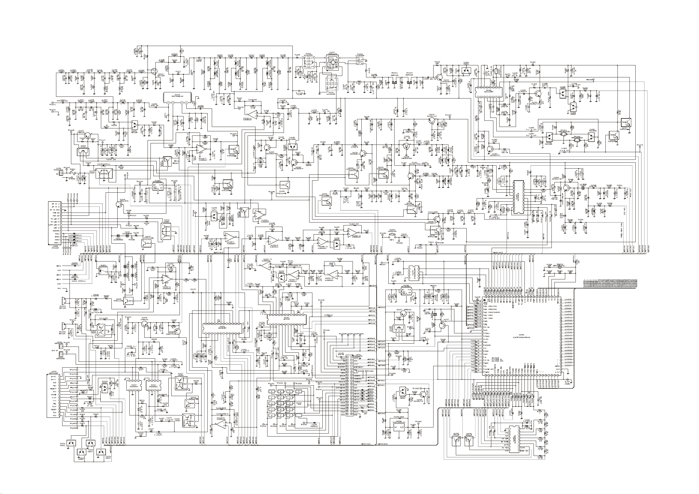
Circuit Diagram
Main Unit
27

Main Unit
Note:
28

Parts Layout
Main Unit
A
B
7
6 5 4 3 2 1
C
TDA2822D
(Q1007,1011)
CPH6102 (AB)
(Q1008, 1037)
UMG2N (G2)
(Q1014)
2SA1774 (FR)
(Q1015)
UMC5N (C5)
(Q1017, 1020)
PDTC144EE (26)
(Q1019, 1024)
Side A
NJM2902V
(Q1018, 1022, 1058)
S-80735SN-DZ (DZ)
(Q1034)
XN1501 (5R)
(Q1035)
TK71635SCL (L35)
(Q1036)
S-93C56AMFN
(Q1040)
2SC4617 (BR)
(Q1042, 1047)
UN911F (60)
(Q1048, 1059)
LC87F72C8A
(Q1050)
BU2090FS
(Q1052)
DA221 (K)
(D1001, 1010, 1012, 1013,
1014, 1034, 1038, 1045)
29

Main Unit
7
6 5 4 3 2 1
a
b
30
c
XP1501 (5R)
(Q1001)
M68732HA-22
(Q1016)
CPH6102 (AB)
(Q1002)
M62364FP
(Q1021)
AK2345
(Q1027)
UMZ2N (Z2)
(Q1003)
PDTC144EE (26)
(Q1023, 1030, 1033,
1045, 1056, 1057)
2SC3356 (R24)
(Q1026)
2SC4227 (R32)
(Q1041)
2SC4617 (BR)
(Q1043, 1051, 1054, 1055)
2SC5226 (R22)
(Q1029, 1032, 1044, 1046)
UMG2N (G2)
(Q1004)
2SK508 (K52)
(Q1038)
2SD1767 (DC)
(Q1005)
TA31136FN
(Q1049)
PDTC114TE
(Q1006, 1010, 1028,
1031, 1039)
SA7025DK
(Q1053)
TK71650SCL (L50)
(Q1009)
RB715F (3D)
(D1021)
MA132WK (MU)
(D1035, 1056, 1060)
BIC702M
(Q1012)
(D 1029, 1054, 1058, 1059)
DA221 (K)
UN911F (60)
(Q1013, 1025)
Side B
GN2011-Q (4W)
(D1037)

Circuit Diagram
Main Unit (Lot. 5~)
31

Main Unit (Lot. 5~)
Note:
32

Parts Layout
Main Unit (Lot. 5~)
A
B
7
6 5 4 3 2 1
C
TDA2822D
(Q1007,1011)
CPH6102 (AB)
(Q1008, 1037)
UMG2N (G2)
(Q1014)
2SA1774 (FR)
(Q1015)
UMC5N (C5)
(Q1017, 1020)
PDTC144EE (26)
(Q1019, 1024)
Side A
NJM2902V
(Q1018, 1022, 1058)
S-80735SN-DZ (DZ)
(Q1034)
XN1501 (5R)
(Q1035)
TK71635SCL (L35)
(Q1036)
S-93C56AMFN
(Q1040)
2SC4617 (BR)
(Q1042, 1047)
UN911F (60)
(Q1048, 1059)
LC87F72C8A
(Q1050)
BU2090FS
(Q1052)
DA221 (K)
(D1001, 1010, 1012, 1013,
1014, 1034, 1038, 1045)
33

Main Unit (Lot. 5~)
7
6 5 4 3 2 1
a
b
34
c
XP1501 (5R)
(Q1001)
M68732HA-22
(Q1016)
CPH6102 (AB)
(Q1002)
M62364FP
(Q1021)
AK2345
(Q1027)
UMZ2N (Z2)
(Q1003)
PDTC144EE (26)
(Q1023, 1030, 1033,
1045, 1056, 1057)
2SC3356 (R24)
(Q1026)
2SC4227 (R32)
(Q1041)
2SC4617 (BR)
(Q1043, 1051, 1054, 1055)
2SC5226 (R22)
(Q1029, 1032, 1044, 1046)
UMG2N (G2)
(Q1004)
2SK508 (K52)
(Q1038)
2SD1767 (DC)
(Q1005)
TA31136FN
(Q1049)
PDTC114TE
(Q1006, 1010, 1028,
1031, 1039)
SA7025DK
(Q1053)
TK71650SCL (L50)
(Q1009)
RB715F (3D)
(D1021)
MA132WK (MU)
(D1035, 1056, 1060)
BIC702M
(Q1012)
(D 1029, 1054, 1058, 1059)
DA221 (K)
Side B
UN911F (60)
(Q1013, 1025)
GN2011-Q (4W)
(D1037)

Main Unit
Parts List
DESCRIPTION VALUE V/W TOL. VXSTD P/NMFR’S DESIG VERS.REF. LOT. SIDE LAY ADR
*** MAIN-UNIT ***
PCB with Components (W/ VR-UNIT) CP6946001 VERSION D
PCB with Components (W/ VR-UNIT) CP6946003 VERSION A
PCB with Components (W/ VR-UNIT) CP6946005 CS VERSION
PCB with Components (W/ VR-UNIT) CP6946007 VERSION A, CE
PCB with Components (W/ VR-UNIT) CP6946008 VERSION CS, CE
PCB with Components (W/ VR-UNIT) CP69460011 VERSION F
Printed Circuit Board FR006560C 1Printed Circuit Board FR006560D 5-
C 1001 CHIP CAP. 150pF 50V CH GRM36CH151J50PT K22178240 1- B c1
C 1002 CHIP CAP. 22pF 50V CH GRM36CH220J50PT K22178220 1- B c2
C 1003 CHIP CAP. 10pF 50V CH GRM36CH100D50PT K22178212 1- B b2
C 1004 CHIP CAP. 0.001uF 50V B GRM36B102K50PT K22178809 1- A C7
C 1005 CHIP CAP. 8pF 50V CH GRM36CH080D50PT K22178210 1-6 B c2
C 1005 CHIP CAP. 9pF 50V CH GRM36CH090D50PT K22178211 CS VERSION 7- B c2
C 1005 CHIP CAP. 12pF 50V CH GRM36CH120J50PT K22178214 VERSION A 7- B c2
C 1005 CHIP CAP. 8pF 50V CH GRM36CH080D50PT K22178210 VERSION D 7- B c2
C 1005 CHIP CAP. 7pF 50V CH GRM36CH070D50PT K22178209 VERSION F 8- B c2
C 1006 CHIP CAP. 0.001uF 50V B GRM36B102K50PT K22178809 1- B a4
C 1007 CHIP CAP. 0.001uF 50V B GRM36B102K50PT K22178809 1- B a4
C 1008 CHIP CAP. 0.01uF 16V B GRM36B103K16PT K22128804 1- A C3
C 1009 CHIP CAP. 2pF 50V CK GRM36CK020C50PT K22178204 1- B c2
C 1009 CHIP CAP. 2pF 50V CK GRM36CK020B50PT K22178289 6 B c2
C 1009 CHIP CAP. 2pF 50V CK GRM36CK020B50PT K22178289 CS VERSION 7- B c2
C 1009 CHIP CAP. 3pF 50V CJ GRM36CJ030B50PT K22178290 VERSION A 7- B c2
C 1009 CHIP CAP. 2pF 50V CK GRM36CK020B50PT K22178289 VERSION D 7- B c2
C 1009 CHIP CAP. 2pF 50V CK GRM36CK020B50PT K22178289 VERSION F 8- B c2
C 1010 CHIP CAP. 0.01uF 16V B GRM36B103K16PT K22128804 1- A C4
C 1011 CHIP CAP. 6pF 50V CH GRM36CH060D50PT K22178208 1-6 B c2
C 1011 CHIP CAP. 6pF 50V CH GRM36CH060D50PT K22178208 CS VERSION 7- B c2
C 1011 CHIP CAP. 8pF 50V CH GRM36CH080D50PT K22178210 VERSION A 7- B c2
C 1011 CHIP CAP. 7pF 50V CH GRM36CH070D50PT K22178209 VERSION A 10- B c2
C 1011 CHIP CAP. 6pF 50V CH GRM36CH060D50PT K22178208 VERSION D 7- B c2
C 1011 CHIP CAP. 5pF 50V CH GRM36CH050C50PT K22178207 VERSION F 8- B c2
C 1013 CHIP CAP. 2pF 50V CK GRM36CK020C50PT K22178204 1- B c2
C 1013 CHIP CAP. 2pF 50V CK GRM36CK020B50PT K22178289 6 B c2
C 1013 CHIP CAP. 2pF 50V CK GRM36CK020B50PT K22178289 CS VERSION 7- B c2
C 1013 CHIP CAP. 3pF 50V CJ GRM36CJ030B50PT K22178290 VERSION A 7- B c2
C 1013 CHIP CAP. 2pF 50V CK GRM36CK020B50PT K22178289 VERSION D 7- B c2
C 1013 CHIP CAP. 2pF 50V CK GRM36CK020B50PT K22178289 VERSION F 8- B c2
C 1015 CHIP CAP. 56pF 50V CH GRM36CH560J50PT K22178230 1- B b2
C 1016 CHIP CAP. 0.0027uF 50V B GRM36B272K50PT K22178814 1- B a4
C 1017 CHIP TA.CAP. 4.7uF 6.3V TMCMA0J475MTR K78080026 1- B a4
C 1018 CHIP CAP. 150pF 50V CH GRM36CH151J50PT K22178240 1- B b2
C 1019 CHIP CAP. 7pF 50V CH GRM36CH070D50PT K22178209 1-6 B c2
C 1019 CHIP CAP. 7pF 50V CH GRM36CH070D50PT K22178209 CS VERSION 7- B c2
C 1019 CHIP CAP. 10pF 50V CH GRM36CH100D50PT K22178212 VERSION A 7- B c2
C 1019 CHIP CAP. 7pF 50V CH GRM36CH070D50PT K22178209 VERSION D 7- B c2
C 1019 CHIP CAP. 6pF 50V CH GRM36CH060D50PT K22178208 VERSION F 8- B c2
C 1020 CHIP CAP. 1pF 50V CK GRM36CK010C50PT K22178202 1-7 B c2
C 1020 CHIP CAP. 1pF 50V CK GRM36CK010C50PT K22178202 CS VERSION 8- B c2
C 1020 CHIP CAP. 1pF 50V CK GRM36CK010C50PT K22178202 VERSION A 8- B c2
C 1020 CHIP CAP. 1pF 50V CK GRM36CK010C50PT K22178202 VERSION D 8- B c2
C 1020 CHIP CAP. 0.5pF 50V CK GRM36CK0R5B50PT K22178285 VERSION F 8- B c2
C 1021 CHIP TA.CAP. 1uF 16V TMCSA1C105MTR K78120023 1- B a7
C 1023 CHIP CAP. 0.1uF 10V B GRM36B104K10PT K22108802 1- B a7
C 1024 CHIP CAP. 0.001uF 50V B GRM36B102K50PT K22178809 1- B b2
C 1025 CHIP CAP. 1pF 50V CK GRM36CK010C50PT K22178202 1-7 B c2
C 1025 CHIP CAP. 1pF 50V CK GRM36CK010C50PT K22178202 CS VERSION 8- B c2
C 1025 CHIP CAP. 1pF 50V CK GRM36CK010C50PT K22178202 VERSION A 8- B c2
35

Main Unit
DESCRIPTION VALUE V/W TOL. VXSTD P/NMFR’S DESIG VERS.REF. LOT. SIDE LAY ADR
C 1025 CHIP CAP. 1pF 50V CK GRM36CK010C50PT K22178202 VERSION D 8- B c2
C 1025 CHIP CAP. 0.5pF 50V CK GRM36CK0R5B50PT K22178285 VERSION F 8- B c2
C 1026 CHIP CAP. 9pF 50V CH GRM36CH090D50PT K22178211 1-6 B b2
C 1026 CHIP CAP. 8pF 50V CH GRM36CH080D50PT K22178210 CS VERSION 7- B b2
C 1026 CHIP CAP. 9pF 50V CH GRM36CH090D50PT K22178211 VERSION A 7- B b2
C 1026 CHIP CAP. 9pF 50V CH GRM36CH090D50PT K22178211 VERSION D 7- B b2
C 1026 CHIP CAP. 10pF 50V CH GRM36CH100D50PT K22178212 VERSION F 8- B b2
C 1027 CHIP TA.CAP. 10uF 6.3V TEMSVA0J106M-8R K78080027 1- B b3
C 1028 CHIP CAP. 7pF 50V CH GRM36CH070D50PT K22178209 1- B c2
C 1029 CHIP CAP. 0.01uF 16V B GRM36B103K16PT K22128804 1- A C1
C 1030 CHIP CAP. 10pF 50V CH GRM36CH100D50PT K22178212 1-6 B b2
C 1030 CHIP CAP. 12pF 50V CH GRM36CH120J50PT K22178214 CS VERSION 7- B b2
C 1030 CHIP CAP. 15pF 50V CH GRM36CH150J50PT K22178216 VERSION A 7- B b2
C 1030 CHIP CAP. 10pF 50V CH GRM36CH100D50PT K22178212 VERSION D 7- B b2
C 1030 CHIP CAP. 9pF 50V CH GRM36CH090D50PT K22178211 VERSION F 8- B b2
C 1031 CHIP CAP. 100pF 50V CH GRM36CH101J50PT K22178236 1- A C3
C 1032 CHIP CAP. 0.01uF 16V B GRM36B103K16PT K22128804 1- B b2
C 1034 CHIP CAP. 0.022uF 16V B GRM36B223K16PT K22128806 1- B a7
C 1035 CHIP CAP. 1.5pF 50V CK GRM36CK1R5C50PT K22178203 1-6 B b2
C 1035 CHIP CAP. 0.5pF 50V CK GRM36CK0R5C50PT K22178201 CS VERSION 7 B b2
C 1035 CHIP CAP. 0.5pF 50V CK GRM36CK0R5B50PT K22178285 CS VERSION 8- B b2
C 1035 CHIP CAP. 1pF 50V CK GRM36CK010C50PT K22178202 VERSION A 7- B b2
C 1035 CHIP CAP. 1.5pF 50V CK GRM36CK1R5C50PT K22178203 VERSION D 7- B b2
C 1036 CHIP CAP. 12pF 50V CH GRM36CH120J50PT K22178214 1-6 B b2
C 1036 CHIP CAP. 12pF 50V CH GRM36CH120J50PT K22178214 CS VERSION 7- B b2
C 1036 CHIP CAP. 15pF 50V CH GRM36CH150J50PT K22178216 VERSION A 7- B b2
C 1036 CHIP CAP. 12pF 50V CH GRM36CH120J50PT K22178214 VERSION D 7- B b2
C 1036 CHIP CAP. 12pF 50V CH GRM36CH120J50PT K22178214 VERSION F 8- B b2
C 1037 CHIP CAP. 150pF 50V CH GRM36CH151J50PT K22178240 1- B b2
C 1038 CHIP CAP. 0.001uF 50V B GRM36B102K50PT K22178809 1- A B4
C 1039 CHIP CAP. 10pF 50V CH GRM36CH100D50PT K22178212 1-6 B b2
C 1039 CHIP CAP. 12pF 50V CH GRM36CH120J50PT K22178214 CS VERSION 7- B b2
C 1039 CHIP CAP. 15pF 50V CH GRM36CH150J50PT K22178216 VERSION A 7- B b2
C 1039 CHIP CAP. 10pF 50V CH GRM36CH100D50PT K22178212 VERSION D 7- B b2
C 1039 CHIP CAP. 9pF 50V CH GRM36CH090D50PT K22178211 VERSION F 8- B b2
C 1040 CHIP CAP. 0.1uF 10V B GRM36B104K10PT K22108802 1- A B3
C 1041 CHIP CAP. 0.1uF 10V B GRM36B104K10PT K22108802 1- A B3
C 1042 CHIP CAP. 1pF 50V CK GRM36CK010C50PT K22178202 1-6 B b2
C 1042 CHIP CAP. 1pF 50V CK GRM36CK010C50PT K22178202 VERSION D 7- B b2
C 1042 CHIP CAP. 0.5pF 50V CK GRM36CK0R5B50PT K22178285 VERSION F 8- B b2
C 1043 CHIP CAP. 7pF 50V CH GRM36CH070D50PT K22178209 1-6 B b2
C 1043 CHIP CAP. 7pF 50V CH GRM36CH070D50PT K22178209 CS VERSION 7- B b2
C 1043 CHIP CAP. 8pF 50V CH GRM36CH080D50PT K22178210 VERSION A 7- B b2
C 1043 CHIP CAP. 7pF 50V CH GRM36CH070D50PT K22178209 VERSION D 7- B b2
C 1043 CHIP CAP. 6pF 50V CH GRM36CH060D50PT K22178208 VERSION F 8- B b2
C 1044 CHIP CAP. 0.01uF 16V B GRM36B103K16PT K22128804 1- B a6
C 1045 CHIP CAP. 150pF 50V CH GRM36CH151J50PT K22178240 1- B b2
C 1046 CHIP TA.CAP. 10uF 6.3V TEMSVA0J106M-8R K78080027 1- A B4
C 1047 CHIP CAP. 0.1uF 10V B GRM36B104K10PT K22108802 1- A B4
C 1048 CHIP TA.CAP. 10uF 16V TEMSVB21C106M-8R K78120025 1- B a6
C 1049 CHIP CAP. 0.001uF 50V B GRM36B102K50PT K22178809 1- B b1
C 1050 CHIP CAP. 0.01uF 16V B GRM36B103K16PT K22128804 1- A B4
C 1051 CHIP CAP. 6pF 50V CH GRM36CH060D50PT K22178208 1-6 B b2
C 1051 CHIP CAP. 6pF 50V CH GRM36CH060D50PT K22178208 CS VERSION 7- B b2
C 1051 CHIP CAP. 5pF 50V CH GRM36CH050C50PT K22178207 VERSION A 7- B b2
C 1051 CHIP CAP. 6pF 50V CH GRM36CH060D50PT K22178208 VERSION D 7- B b2
C 1051 CHIP CAP. 5pF 50V CH GRM36CH050C50PT K22178207 VERSION F 8- B b2
C 1052 CHIP CAP. 100pF 50V CH GRM36CH101J50PT K22178236 1- B c2
C 1053 CHIP CAP. 1uF 10V B GRM40B105K10PT K22100802 1- A B3
C 1053 CHIP CAP. 1uF 10V B GRM40B105K10PT(0.85) K22100803 6- A B3
36

Main Unit
DESCRIPTION VALUE V/W TOL. VXSTD P/NMFR’S DESIG VERS.REF. LOT. SIDE LAY ADR
C 1054 CHIP CAP. 0.01uF 16V B GRM36B103K16PT K22128804 1- B a6
C 1055 CHIP CAP. 150pF 50V CH GRM36CH151J50PT K22178240 1- B b1
C 1056 CHIP CAP. 0.001uF 50V B GRM36B102K50PT K22178809 1- B c2
C 1057 CHIP CAP. 0.1uF 10V B GRM36B104K10PT K22108802 1- A B3
C 1058 CHIP CAP. 0.1uF 10V B GRM36B104K10PT K22108802 1- A B4
C 1060 CHIP CAP. 150pF 50V CH GRM36CH151J50PT K22178240 1- B b3
C 1061 CHIP TA.CAP. 10uF 10V TEMSVA1A106M-8R K78100028 1- A B4
C 1062 CHIP CAP. 0.1uF 10V B GRM36B104K10PT K22108802 1- A B4
C 1063 CHIP CAP. 0.001uF 50V B GRM36B102K50PT K22178809 1- A B3
C 1064 CHIP TA.CAP. 10uF 6.3V TEMSVA0J106M-8R K78080027 1- A B4
C 1065 AL.ELECTRO.CAP. 100uF 10V UVR1A101MDA6 100UF K40109028 1- A B4
C 1067 CHIP CAP. 0.001uF 50V B GRM36B102K50PT K22178809 1- B b1
C 1068 CHIP CAP. 0.1uF 10V B GRM36B104K10PT K22108802 1- A B3
C 1069 CHIP CAP. 0.1uF 10V B GRM36B104K10PT K22108802 1- A B4
C 1070 CHIP CAP. 0.1uF 10V B GRM36B104K10PT K22108802 1- A B4
C 1071 CHIP CAP. 2pF 50V CK GRM36CK020B50PT K22178289 VERSION A 9- B b3
C 1072 CHIP CAP. 10pF 50V CH GRM36CH100D50PT K22178212 1- A B3
C 1073 CHIP CAP. 0.01uF 16V B GRM36B103K16PT K22128804 1- B a6
C 1074 CHIP CAP. 0.1uF 10V B GRM36B104K10PT K22108802 1- A B3
C 1075 CHIP CAP. 0.01uF 16V B GRM36B103K16PT K22128804 1- B a6
C 1076 CHIP CAP. 0.01uF 16V B GRM36B103K16PT K22128804 1- A B3
C 1078 CHIP TA.CAP. 10uF 16V TEMSVB21C106M-8R K78120025 1- A A3
C 1079 CHIP CAP. 0.1uF 10V B GRM36B104K10PT K22108802 1- A B3
C 1080 CHIP TA.CAP. 10uF 6.3V TEMSVA0J106M-8R K78080027 1- B a6
C 1082 CHIP CAP. 0.001uF 50V B GRM36B102K50PT K22178809 1- B b3
C 1083 CHIP CAP. 10pF 50V CH GRM36CH100D50PT K22178212 1-6 B b2
C 1083 CHIP CAP. 10pF 50V CH GRM36CH100D50PT K22178212 CS VERSION 7- B b2
C 1083 CHIP CAP. 12pF 50V CH GRM36CH120J50PT K22178214 VERSION A 7- B b2
C 1083 CHIP CAP. 10pF 50V CH GRM36CH100D50PT K22178212 VERSION D 7- B b2
C 1083 CHIP CAP. 4pF 50V CH GRM36CH040C50PT K22178206 VERSION F 8- B b2
C 1084 CHIP CAP. 0.001uF 50V B GRM36B102K50PT K22178809 1- B b1
C 1085 CHIP TA.CAP. 1uF 16V TMCSA1C105MTR K78120023 1- A A4
C 1086 CHIP CAP. 0.01uF 16V B GRM36B103K16PT K22128804 1- A A4
C 1087 CHIP CAP. 0.1uF 10V B GRM36B104K10PT K22108802 1- A A4
C 1088 CHIP CAP. 0.01uF 16V B GRM36B103K16PT K22128804 1- A A4
C 1091 CHIP TA.CAP. 10uF 6.3V TEMSVA0J106M-8R K78080027 1- B c5
C 1092 CHIP CAP. 150pF 50V CH GRM36CH151J50PT K22178240 1- B b4
C 1093 CHIP CAP. 0.01uF 16V B GRM36B103K16PT K22128804 1- B c5
C 1094 CHIP CAP. 4pF 50V CH GRM36CH040C50PT K22178206 1-6 B a1
C 1094 CHIP CAP. 6pF 50V CH GRM36CH060D50PT K22178208 CS VERSION 7- B a1
C 1094 CHIP CAP. 5pF 50V CH GRM36CH050C50PT K22178207 CS VERSION 13- B a1
C 1094 CHIP CAP. 4pF 50V CH GRM36CH040C50PT K22178206 VERSION A 7- B a1
C 1094 CHIP CAP. 4pF 50V CH GRM36CH040C50PT K22178206 VERSION D 7- B a1
C 1094 CHIP CAP. 3pF 50V CJ GRM36CJ030C50PT K22178205 VERSION F 8- B a1
C 1096 CHIP CAP. 0.001uF 50V B GRM36B102K50PT K22178809 1- B c5
C 1097 CHIP CAP. 15pF 50V CH GRM36CH150J50PT K22178216 1-6 B a2
C 1097 CHIP CAP. 15pF 50V CH GRM36CH150J50PT K22178216 CS VERSION 7- B a2
C 1097 CHIP CAP. 18pF 50V CH GRM36CH180J50PT K22178218 VERSION A 7- B a2
C 1097 CHIP CAP. 15pF 50V CH GRM36CH150J50PT K22178216 VERSION D 7- B a2
C 1097 CHIP CAP. 15pF 50V CH GRM36CH150J50PT K22178216 VERSION F 8- B a2
C 1098 CHIP CAP. 0.001uF 50V B GRM36B102K50PT K22178809 1- A A4
C 1099 CHIP CAP. 0.01uF 16V B GRM36B103K16PT K22128804 1- B b2
C 1100 CHIP CAP. 0.01uF 16V B GRM36B103K16PT K22128804 1- A A4
C 1101 CHIP CAP. 0.1uF 10V B GRM36B104K10PT K22108802 1- A A4
C 1102 CHIP CAP. 0.1uF 10V B GRM36B104K10PT K22108802 1- B a6
C 1104 CHIP TA.CAP. 4.7uF 6.3V TEMSVA0J475M-8R K78080017 1- A A4
C 1105 CHIP CAP. 22pF 50V CH GRM36CH220J50PT K22178220 1-6 B a2
C 1105 CHIP CAP. 27pF 50V CH GRM36CH270J50PT K22178222 CS VERSION 7- B a2
C 1105 CHIP CAP. 22pF 50V CH GRM36CH220J50PT K22178220 VERSION A 7- B a2
C 1105 CHIP CAP. 27pF 50V CH GRM36CH270J50PT K22178222 VERSION A 13- B a2
37

Main Unit
DESCRIPTION VALUE V/W TOL. VXSTD P/NMFR’S DESIG VERS.REF. LOT. SIDE LAY ADR
C 1105 CHIP CAP. 22pF 50V CH GRM36CH220J50PT K22178220 VERSION D 7- B a2
C 1105 CHIP CAP. 22pF 50V CH GRM36CH220J50PT K22178220 VERSION F 8- B a2
C 1106 CHIP CAP. 10pF 50V CH GRM36CH100D50PT K22178212 1-6 B a2
C 1106 CHIP CAP. 12pF 50V CH GRM36CH120J50PT K22178214 CS VERSION 7- B a2
C 1106 CHIP CAP. 9pF 50V CH GRM36CH090D50PT K22178211 VERSION A 7- B a2
C 1106 CHIP CAP. 10pF 50V CH GRM36CH100D50PT K22178212 VERSION D 7- B a2
C 1106 CHIP CAP. 8pF 50V CH GRM36CH080D50PT K22178210 VERSION F 8- B a2
C 1107 CHIP CAP. 0.001uF 50V B GRM36B102K50PT K22178809 1- B c5
C 1108 CHIP CAP. 0.001uF 50V B GRM36B102K50PT K22178809 1- B b2
C 1109 CHIP CAP. 680pF 50V B GRM36B681K50PT K22178807 1- A A4
C 1110 CHIP CAP. 0.0047uF 25V B GRM36B472K25PT K22148830 1- A A4
C 1112 CHIP CAP. 150pF 50V CH GRM36CH151J50PT K22178240 1- B b2
C 1113 CHIP CAP. 0.1uF 10V B GRM36B104K10PT K22108802 1- B c5
C 1114 CHIP CAP. 0.0027uF 50V B GRM36B272K50PT K22178814 1- A A4
C 1115 CHIP CAP. 4pF 50V CH GRM36CH040C50PT K22178206 1-6 B a2
C 1115 CHIP CAP. 6pF 50V CH GRM36CH060D50PT K22178208 CS VERSION 7- B a2
C 1115 CHIP CAP. 5pF 50V CH GRM36CH050C50PT K22178207 CS VERSION 13- B a2
C 1115 CHIP CAP. 4pF 50V CH GRM36CH040C50PT K22178206 VERSION A 7- B a2
C 1115 CHIP CAP. 4pF 50V CH GRM36CH040C50PT K22178206 VERSION D 7- B a2
C 1115 CHIP CAP. 3pF 50V CJ GRM36CJ030C50PT K22178205 VERSION F 8- B a2
C 1116 CHIP CAP. 0.1uF 10V B GRM36B104K10PT K22108802 1- A A4
C 1117 CHIP CAP. 6pF 50V CH GRM36CH060D50PT K22178208 1-6 B a2
C 1117 CHIP CAP. 5pF 50V CH GRM36CH050C50PT K22178207 CS VERSION 7- B a2
C 1117 CHIP CAP. 6pF 50V CH GRM36CH060D50PT K22178208 VERSION A 7- B a2
C 1117 CHIP CAP. 6pF 50V CH GRM36CH060D50PT K22178208 VERSION D 7- B a2
C 1117 CHIP CAP. 4pF 50V CH GRM36CH040C50PT K22178206 VERSION F 8- B a2
C 1118 CHIP CAP. 0.01uF 16V B GRM36B103K16PT K22128804 1- A B3
C 1119 CHIP CAP. 0.0047uF 25V B GRM36B472K25PT K22148830 1- B b6
C 1120 CHIP CAP. 0.1uF 10V B GRM36B104K10PT K22108802 1- B c6
C 1121 CHIP CAP. 39pF 50V CH GRM36CH390J50PT K22178226 1-6 B a2
C 1121 CHIP CAP. 39pF 50V CH GRM36CH390J50PT K22178226 CS VERSION 7- B a2
C 1121 CHIP CAP. 33pF 50V CH GRM36CH330J50PT K22178224 VERSION A 7- B a2
C 1121 CHIP CAP. 39pF 50V CH GRM36CH390J50PT K22178226 VERSION D 7- B a2
C 1121 CHIP CAP. 39pF 50V CH GRM36CH390J50PT K22178226 VERSION F 8- B a2
C 1123 CHIP CAP. 15pF 50V CH GRM36CH150J50PT K22178216 1- B a2
C 1124 CHIP CAP. 0.001uF 50V B GRM36B102K50PT K22178809 1- B b7
C 1125 CHIP CAP. 0.0047uF 25V B GRM36B472K25PT K22148830 1- B b7
C 1126 CHIP CAP. 0.1uF 10V B GRM36B104K10PT K22108802 1- B b7
C 1127 CHIP CAP. 0.001uF 50V B GRM36B102K50PT K22178809 1- B c4
C 1128 CHIP CAP. 150pF 50V CH GRM36CH151J50PT K22178240 1- B c4
C 1129 CHIP CAP. 0.01uF 16V B GRM36B103K16PT K22128804 1- A B3
C 1130 CHIP CAP. 0.0047uF 25V B GRM36B472K25PT K22148830 1- B b7
C 1132 CHIP CAP. 1uF 10V B GRM40B105K10PT K22100802 1-2 B b6
C 1133 CHIP CAP. 0.01uF 16V B GRM36B103K16PT K22128804 1- B b7
C 1134 CHIP CAP. 4pF 50V CH GRM36CH040C50PT K22178206 1-6 B a2
C 1134 CHIP CAP. 6pF 50V CH GRM36CH060D50PT K22178208 CS VERSION 7- B a2
C 1134 CHIP CAP. 5pF 50V CH GRM36CH050C50PT K22178207 CS VERSION 13- B a2
C 1134 CHIP CAP. 4pF 50V CH GRM36CH040C50PT K22178206 VERSION A 7- B a2
C 1134 CHIP CAP. 4pF 50V CH GRM36CH040C50PT K22178206 VERSION D 7- B a2
C 1134 CHIP CAP. 3pF 50V CJ GRM36CJ030C50PT K22178205 VERSION F 8- B a2
C 1135 CHIP CAP. 68pF 50V CH GRM36CH680J50PT K22178232 1- B c6
C 1136 CHIP CAP. 33pF 50V CH GRM36CH330J50PT K22178224 1- B b7
C 1137 CHIP CAP. 0.0047uF 25V B GRM36B472K25PT K22148830 1- B b7
C 1138 CHIP CAP. 0.01uF 16V B GRM36B103K16PT K22128804 1- A B3
C 1139 CHIP CAP. 6pF 50V CH GRM36CH060D50PT K22178208 1- B a2
C 1140 CHIP TA.CAP. 1uF 16V TMCSA1C105MTR K78120023 1- A B3
C 1141 CHIP CAP. 120pF 50V CH GRM36CH121J50PT K22178238 1- B c6
C 1143 CHIP CAP. 0.01uF 16V B GRM36B103K16PT K22128804 1- A A4
C 1144 CHIP CAP. 4pF 50V CH GRM36CH040C50PT K22178206 1- B b4
C 1145 CHIP CAP. 5pF 50V CH GRM36CH050C50PT K22178207 1- B a2
38

Main Unit
DESCRIPTION VALUE V/W TOL. VXSTD P/NMFR’S DESIG VERS.REF. LOT. SIDE LAY ADR
C 1146 CHIP CAP. 0.001uF 50V B GRM36B102K50PT K22178809 1- B b5
C 1147 CHIP CAP. 100pF 50V CH GRM36CH101J50PT K22178236 1- B c7
C 1148 CHIP CAP. 0.001uF 50V B GRM36B102K50PT K22178809 1- B b4
C 1149 CHIP TA.CAP. 1uF 16V TMCSA1C105MTR K78120023 1- B c6
C 1150 CHIP CAP. 150pF 50V CH GRM36CH151J50PT K22178240 1- B b4
C 1151 CHIP CAP. 0.001uF 50V B GRM36B102K50PT K22178809 1- B b4
C 1152 CHIP CAP. 0.01uF 16V B GRM36B103K16PT K22128804 1- A C3
C 1153 CHIP CAP. 150pF 50V CH GRM36CH151J50PT K22178240 1- B a2
C 1154 CHIP TA.CAP. 1uF 16V TMCSA1C105MTR K78120023 1- B c6
C 1155 CHIP CAP. 150pF 50V CH GRM36CH151J50PT K22178240 1- A C3
C 1157 CHIP CAP. 0.1uF 10V B GRM36B104K10PT K22108802 1- B a2
C 1158 CHIP CAP. 0.001uF 50V B GRM36B102K50PT K22178809 1- B b4
C 1159 CHIP CAP. 100pF 50V CH GRM36CH101J50PT K22178236 1- B c7
C 1160 CHIP CAP. 100pF 50V CH GRM36CH101J50PT K22178236 1- B c7
C 1161 CHIP CAP. 0.01uF 16V B GRM36B103K16PT K22128804 1- A C2
C 1162 CHIP TA.CAP. 4.7uF 6.3V TMCMA0J475MTR K78080026 1- B c6
C 1164 CHIP CAP. 33pF 50V CH GRM36CH330J50PT K22178224 1- B b4
C 1166 CHIP CAP. 0.022uF 16V B GRM36B223K16PT K22128806 1- A C3
C 1168 CHIP CAP. 0.01uF 16V B GRM36B103K16PT K22128804 1- B a2
C 1169 CHIP CAP. 10pF 50V CH GRM36CH100D50PT K22178212 1- B c7
C 1170 CHIP CAP. 150pF 50V CH GRM36CH151J50PT K22178240 1- B a2
C 1171 CHIP CAP. 0.01uF 16V B GRM36B103K16PT K22128804 1- A C3
C 1172 CHIP CAP. 3pF 50V CJ GRM36CJ030C50PT K22178205 1- B b5
C 1174 CHIP CAP. 100pF 50V CH GRM36CH101J50PT K22178236 1- A B2
C 1175 CHIP CAP. 47pF 50V CH GRM36CH470J50PT K22178228 1- B b2
C 1176 CHIP CAP. 5pF 50V CH GRM36CH050C50PT K22178207 1- B b4
C 1177 CHIP CAP. 330pF 50V B GRM36B331K50PT K22178803 1- A C3
C 1178 CHIP CAP. 2pF 50V CK GRM36CK020C50PT K22178204 1- B b2
C 1178 CHIP CAP. 2pF 50V CK GRM36CK020B50PT K22178289 6- B b2
C 1179 CHIP CAP. 10pF 50V CH GRM36CH100D50PT K22178212 1- B b7
C 1180 CHIP TA.CAP. 10uF 6.3V TEMSVA0J106M-8R K78080027 1- B b4
C 1181 CHIP CAP. 7pF 50V CH GRM36CH070D50PT K22178209 1- B b4
C 1182 CHIP CAP. 0.047uF 10V B GRM36B473K10PT K22108801 1- B b4
C 1183 CHIP CAP. 1uF 10V B GRM40B105K10PT K22100802 1- A B2
C 1183 CHIP CAP. 1uF 10V B GRM40B105K10PT(0.85) K22100803 6- A B2
C 1184 CHIP CAP. 0.01uF 16V B GRM36B103K16PT K22128804 1- B a2
C 1185 CHIP CAP. 0.001uF 50V B GRM36B102K50PT K22178809 1- B b4
C 1186 CHIP CAP. 0.01uF 16V B GRM36B103K16PT K22128804 1- A C3
C 1187 CHIP CAP. 150pF 50V CH GRM36CH151J50PT K22178240 1- B a2
C 1188 CHIP CAP. 0.001uF 50V B GRM36B102K50PT K22178809 1- B b4
C 1189 CHIP CAP. 150pF 50V CH GRM36CH151J50PT K22178240 1- B b4
C 1190 CHIP CAP. 0.047uF 10V B GRM36B473K10PT K22108801 1- B b4
C 1191 CHIP CAP. 0.01uF 16V B GRM36B103K16PT K22128804 1- A C3
C 1192 CHIP CAP. 0.001uF 50V B GRM36B102K50PT K22178809 1- B b2
C 1193 CHIP CAP. 0.01uF 16V B GRM36B103K16PT K22128804 1- B b2
C 1194 CHIP CAP. 150pF 50V CH GRM36CH151J50PT K22178240 1- B b4
C 1195 CHIP CAP. 2pF 50V CK GRM36CK020C50PT K22178204 1- B b4
C 1195 CHIP CAP. 2pF 50V CK GRM36CK020B50PT K22178289 6- B b4
C 1196 CHIP CAP. 33pF 50V CH GRM36CH330J50PT K22178224 1- B a3
C 1196 CHIP CAP. 27pF 50V CH GRM36CH270J50PT K22178222 6- B a3
C 1196 CHIP CAP. 33pF 50V CH GRM36CH330J50PT K22178224 8- B a3
C 1198 CHIP CAP. 0.001uF 50V B GRM36B102K50PT K22178809 1- B b4
C 1199 CHIP CAP. 2pF 50V CK GRM36CK020C50PT K22178204 1- B b3
C 1199 CHIP CAP. 2pF 50V CK GRM36CK020B50PT K22178289 6- B b3
C 1201 CHIP CAP. 0.01uF 16V B GRM36B103K16PT K22128804 1- A B3
C 1202 CHIP TA.CAP. 10uF 6.3V EEJK0JS106R K78080079 1- B b3
C 1202 CHIP TA.CAP. 10uF 6.3V EEJK0JS106R K78080079 13- B b3
C 1203 CHIP CAP. 150pF 50V CH GRM36CH151J50PT K22178240 1- B b3
C 1204 CHIP CAP. 0.001uF 50V B GRM36B102K50PT K22178809 1- A A4
C 1205 CHIP CAP. 0.001uF 50V B GRM36B102K50PT K22178809 1- A A2
39

Main Unit
DESCRIPTION VALUE V/W TOL. VXSTD P/NMFR’S DESIG VERS.REF. LOT. SIDE LAY ADR
C 1206 CHIP CAP. 0.1uF 10V B GRM36B104K10PT K22108802 1- A A2
C 1207 CHIP TA.CAP. 4.7uF 16V TEMSVA1C475M-8R K78120031 1- A A3
C 1208 CHIP CAP. 0.1uF 10V B GRM36B104K10PT K22108802 1- A B3
C 1209 CHIP TA.CAP. 10uF 6.3V TEMSVA0J106M-8R K78080027 1- B a4
C 1210 CHIP CAP. 10pF 50V CH GRM36CH100D50PT K22178212 1- B b3
C 1212 CHIP CAP. 10pF 50V CH GRM36CH100D50PT K22178212 1- B a4
C 1212 CHIP CAP. 15pF 50V CH GRM36CH150J50PT K22178216 6- B a4
C 1213 CHIP CAP. 2pF 50V CK GRM36CK020C50PT K22178204 1- B b4
C 1213 CHIP CAP. 2pF 50V CK GRM36CK020B50PT K22178289 6- B b4
C 1214 CHIP CAP. 0.001uF 50V B GRM36B102K50PT K22178809 1- B a4
C 1215 CHIP CAP. 6pF 50V CH GRM36CH060D50PT K22178208 1-7 B b3
C 1215 CHIP CAP. 6pF 50V CH GRM36CH060D50PT K22178208 CS VERSION 8- B b3
C 1215 CHIP CAP. 6pF 50V CH GRM36CH060D50PT K22178208 VERSION A 8- B b3
C 1215 CHIP CAP. 6pF 50V CH GRM36CH060D50PT K22178208 VERSION D 8- B b3
C 1215 CHIP CAP. 7pF 50V CH GRM36CH070D50PT K22178209 VERSION F 8- B b3
C 1216 CHIP CAP. 150pF 50V CH GRM36CH151J50PT K22178240 1- B b3
C 1217 CHIP CAP. 0.001uF 50V B GRM36B102K50PT K22178809 1- A B3
C 1218 CHIP CAP. 0.01uF 16V B GRM36B103K16PT K22128804 1- A B3
C 1219 CHIP CAP. 18pF 50V CH GRM36CH180J50PT K22178218 1-6 B b4
C 1219 CHIP CAP. 18pF 50V CH GRM36CH180J50PT K22178218 CS VERSION 7- B b4
C 1219 CHIP CAP. 22pF 50V CH GRM36CH220J50PT K22178220 VERSION A 7- B b4
C 1219 CHIP CAP. 18pF 50V CH GRM36CH180J50PT K22178218 VERSION D 7- B b4
C 1219 CHIP CAP. 12pF 50V CH GRM36CH120J50PT K22178214 VERSION F 8- B b4
C 1220 CHIP TA.CAP. 4.7uF 6.3V TEMSVA0J475M-8R K78080017 1- A A4
C 1221 CHIP CAP. 4pF 50V CH GRM36CH040C50PT K22178206 1-6 B b3
C 1221 CHIP CAP. 4pF 50V CH GRM36CH040C50PT K22178206 CS VERSION 7- B b3
C 1221 CHIP CAP. 3pF 50V CJ GRM36CJ030C50PT K22178205 VERSION A 7- B b3
C 1221 CHIP CAP. 4pF 50V CH GRM36CH040C50PT K22178206 VERSION D 7- B b3
C 1221 CHIP CAP. 4pF 50V CH GRM36CH040C50PT K22178206 VERSION F 8- B b3
C 1222 CHIP CAP. 0.01uF 16V B GRM36B103K16PT K22128804 1- A A3
C 1223 CHIP CAP. 47pF 50V CH GRM36CH470J50PT K22178228 1- B b3
C 1224 CHIP CAP. 18pF 50V CH GRM36CH180J50PT K22178218 1-7 B b4
C 1224 CHIP CAP. 18pF 50V CH GRM36CH180J50PT K22178218 CS VERSION 8- B b4
C 1224 CHIP CAP. 18pF 50V CH GRM36CH180J50PT K22178218 VERSION A 8- B b4
C 1224 CHIP CAP. 18pF 50V CH GRM36CH180J50PT K22178218 VERSION D 8- B b4
C 1224 CHIP CAP. 12pF 50V CH GRM36CH120J50PT K22178214 VERSION F 8- B b4
C 1225 CHIP CAP. 0.001uF 50V B GRM36B102K50PT K22178809 1- A B3
C 1226 CHIP CAP. 0.1uF 10V B GRM36B104K10PT K22108802 1- A A3
C 1227 CHIP CAP. 150pF 50V CH GRM36CH151J50PT K22178240 1-8 B b3
C 1227 CHIP CAP. 150pF 50V CH GRM36CH151J50PT K22178240 CS VERSION 9- B b3
C 1227 CHIP CAP. 150pF 50V CH GRM36CH151J50PT K22178240 VERSION A 9- B b3
C 1227 CHIP CAP. 150pF 50V CH GRM36CH151J50PT K22178240 VERSION F 9- B b3
C 1228 CHIP CAP. 0.001uF 50V B GRM36B102K50PT K22178809 1- A A3
C 1229 CHIP CAP. 27pF 50V CH GRM36CH270J50PT K22178222 1- B a4
C 1229 CHIP CAP. 22pF 50V CH GRM36CH220J50PT K22178220 8- B a4
C 1230 CHIP CAP. 150pF 50V CH GRM36CH151J50PT K22178240 1- B b4
C 1231 CHIP CAP. 15pF 50V CH GRM36CH150J50PT K22178216 1- A A3
C 1232 CHIP CAP. 15pF 50V CH GRM36CH150J50PT K22178216 1- A A3
C 1233 CHIP TA.CAP. 4.7uF 6.3V TMCMA0J475MTR K78080026 1- A A3
C 1234 CHIP CAP. 0.001uF 50V B GRM36B102K50PT K22178809 1- A B3
C 1235 CHIP CAP. 0.001uF 50V B GRM36B102K50PT K22178809 1- B b3
C 1236 CHIP CAP. 6pF 50V CH GRM36CH060D50PT K22178208 1-7 B b3
C 1236 CHIP CAP. 6pF 50V CH GRM36CH060D50PT K22178208 CS VERSION 8- B b3
C 1236 CHIP CAP. 6pF 50V CH GRM36CH060D50PT K22178208 VERSION A 8- B b3
C 1236 CHIP CAP. 6pF 50V CH GRM36CH060D50PT K22178208 VERSION D 8- B b3
C 1236 CHIP CAP. 10pF 50V CH GRM36CH100D50PT K22178212 VERSION F 8- B b3
C 1237 CHIP CAP. 10pF 50V CH GRM36CH100D50PT K22178212 1-6 B b3
C 1237 CHIP CAP. 10pF 50V CH GRM36CH100D50PT K22178212 CS VERSION 7- B b3
C 1237 CHIP CAP. 9pF 50V CH GRM36CH090D50PT K22178211 VERSION A 7- B b3
C 1237 CHIP CAP. 10pF 50V CH GRM36CH100D50PT K22178212 VERSION D 7- B b3
40

Main Unit
DESCRIPTION VALUE V/W TOL. VXSTD P/NMFR’S DESIG VERS.REF. LOT. SIDE LAY ADR
C 1237 CHIP CAP. 8pF 50V CH GRM36CH080D50PT K22178210 VERSION F 8- B b3
C 1238 CHIP TA.CAP. 10uF 6.3V EEJK0JS106R K78080079 1- B b3
C 1238 CHIP TA.CAP. 10uF 6.3V EEJK0JS106R K78080079 13- B b3
C 1239 CHIP CAP. 2pF 50V CK GRM36CK020C50PT K22178204 VERSION A 7 B b3
C 1239 CHIP CAP. 2pF 50V CK GRM36CK020B50PT K22178289 VERSION A 8- B b3
C 1239 CHIP CAP. 2pF 50V CK GRM36CK020B50PT K22178289 VERSION F 8- B b3
C 1240 CHIP TA.CAP. 4.7uF 6.3V TEMSVA0J475M-8R K78080017 1- A A2
C 1241 CHIP CAP. 15pF 50V CH GRM36CH150J50PT K22178216 1- B a4
C 1242 CHIP CAP. 0.01uF 16V B GRM36B103K16PT K22128804 1- B a4
C 1243 CHIP CAP. 0.01uF 16V B GRM36B103K16PT K22128804 1- A A2
C 1244 CHIP CAP. 0.001uF 50V B GRM36B102K50PT K22178809 1- B b5
C 1245 CHIP CAP. 0.01uF 16V B GRM36B103K16PT K22128804 1- B a4
C 1246 CHIP CAP. 47pF 50V CH GRM36CH470J50PT K22178228 1- B b5
C 1247 CHIP CAP. 100pF 50V CH GRM36CH101J50PT K22178236 1- B b3
C 1248 CHIP CAP. 3pF 50V CJ GRM36CJ030C50PT K22178205 1- B b5
C 1249 CHIP CAP. 0.001uF 50V B GRM36B102K50PT K22178809 1- B b5
C 1250 CHIP CAP. 0.001uF 50V B GRM36B102K50PT K22178809 1- B b5
C 1251 CHIP CAP. 0.047uF 10V B GRM36B473K10PT K22108801 1- B a5
C 1252 CHIP CAP. 7pF 50V CH GRM36CH070D50PT K22178209 1- B b5
C 1253 CHIP CAP. 0.01uF 16V B GRM36B103K16PT K22128804 1- A A2
C 1254 CHIP TA.CAP. 0.1uF 20V SKF-1D104M-RP K78130049 1- B b5
C 1254 CHIP TA.CAP. 0.1uF 35V TESVA1V104M1-8R K78160025 5- B b5
C 1256 CHIP CAP. 150pF 50V CH GRM36CH151J50PT K22178240 1- B a4
C 1257 CHIP CAP. 22pF 50V CH GRM36CH220J50PT K22178220 1- B a5
C 1258 CHIP CAP. 39pF 50V CH GRM36CH390J50PT K22178226 1- B b6
C 1259 CHIP CAP. 0.01uF 16V B GRM36B103K16PT K22128804 1- B b6
C 1261 CHIP CAP. 10pF 50V CH GRM36CH100D50PT K22178212 1- B a5
C 1262 CHIP CAP. 0.1uF 10V B GRM36B104K10PT K22108802 1- B b5
C 1264 CHIP CAP. 0.01uF 16V B GRM36B103K16PT K22128804 1- B a5
C 1265 CHIP CAP. 0.047uF 10V B GRM36B473K10PT K22108801 1- B b5
C 1266 CHIP TA.CAP. 1uF 16V TMCSA1C105MTR K78120023 1- B b5
C 1267 CHIP CAP. 56pF 50V CH GRM36CH560J50PT K22178230 1- B a5
C 1268 CHIP CAP. 0.1uF 10V B GRM36B104K10PT K22108802 1- B a5
C 1269 CHIP CAP. 0.1uF 10V B GRM36B104K10PT K22108802 1- B b5
C 1270 CHIP CAP. 0.047uF 10V B GRM36B473K10PT K22108801 1- B b5
C 1271 CHIP CAP. 0.001uF 50V B GRM36B102K50PT K22178809 1- B b5
C 1272 CHIP CAP. 33pF 50V CH GRM36CH330J50PT K22178224 1- B b6
C 1273 CHIP CAP. 0.1uF 10V B GRM36B104K10PT K22108802 1- B b5
C 1274 CHIP CAP. 100pF 50V CH GRM36CH101J50PT K22178236 1- B a5
C 1275 CHIP CAP. 100pF 50V CH GRM36CH101J50PT K22178236 1- B a5
C 1276 CHIP CAP. 0.1uF 10V B GRM36B104K10PT K22108802 1- B b5
C 1277 CHIP CAP. 0.0047uF 25V B GRM36B472K25PT K22148830 1- B a5
C 1278 CHIP CAP. 0.1uF 10V B GRM36B104K10PT K22108802 1- B a5
C 1279 CHIP CAP. 1uF 10V B GRM40B105K10PT K22100802 1- A B2
C 1279 CHIP CAP. 1uF 10V B GRM40B105K10PT(0.85) K22100803 6- A B2
C 1280 CHIP CAP. 0.0056uF 25V B GRM36B562K50PT K22148802 1- B b5
C 1281 CHIP TA.CAP. 10uF 6.3V TEMSVA0J106M-8R K78080027 1- B a5
C 1282 CHIP CAP. 0.0018uF 50V B GRM36B182K50PT K22178812 1- B b5
C 1283 CHIP CAP. 0.01uF 16V B GRM36B103K16PT K22128804 1- B a5
C 1284 CHIP CAP. 0.001uF 50V B GRM36B102K50PT K22178809 1- B b5
C 1285 CHIP CAP. 0.1uF 10V B GRM36B104K10PT K22108802 1- B b5
C 1286 CHIP CAP. 0.1uF 10V B GRM36B104K10PT K22108802 1- B a6
C 1287 CHIP CAP. 0.1uF 10V B GRM36B104K10PT K22108802 1- B a5
C 1288 CHIP CAP. 100pF 50V CH GRM36CH101J50PT K22178236 1- B b5
C 1289 CHIP CAP. 0.1uF 10V B GRM36B104K10PT K22108802 1- A C2
C 1290 CHIP CAP. 0.1uF 10V B GRM36B104K10PT K22108802 1- B b5
C 1291 CHIP TA.CAP. 10uF 6.3V TEMSVA0J106M-8R K78080027 1- B b5
C 1292 CHIP CAP. 47pF 50V CH GRM36CH470J50PT K22178228 1- B b5
C 1294 CHIP CAP. 0.001uF 50V B GRM36B102K50PT K22178809 1- B b5
C 1295 CHIP CAP. 0.1uF 10V B GRM36B104K10PT K22108802 1- B b5
41

Main Unit
DESCRIPTION VALUE V/W TOL. VXSTD P/NMFR’S DESIG VERS.REF. LOT. SIDE LAY ADR
C 1296 CHIP CAP. 0.1uF 10V B GRM36B104K10PT K22108802 1- B a5
C 1297 CHIP CAP. 0.1uF 10V B GRM36B104K10PT K22108802 1- B b5
C 1298 CHIP CAP. 0.047uF 10V B GRM36B473K10PT K22108801 1- B a5
C 1299 CHIP CAP. 56pF 50V CH GRM36CH560J50PT K22178230 1- B b6
C 1300 CHIP CAP. 100pF 50V CH GRM36CH101J50PT K22178236 1- B b6
C 1301 CHIP CAP. 100pF 50V CH GRM36CH101J50PT K22178236 1- B b5
C 1302 CHIP CAP. 82pF 50V CH GRM36CH820J50PT K22178234 1- B b6
C 1303 CHIP CAP. 0.1uF 10V B GRM36B104K10PT K22108802 1- B a6
C 1304 CHIP CAP. 0.001uF 50V B GRM36B102K50PT K22178809 1- B b6
C 1305 CHIP CAP. 0.1uF 10V B GRM36B104K10PT K22108802 1- A B2
C 1306 CHIP CAP. 0.01uF 16V B GRM36B103K16PT K22128804 1- B b5
C 1307 CHIP CAP. 560pF 50V B GRM36B561K50PT K22178806 1- B b5
C 1308 CHIP CAP. 0.01uF 16V B GRM36B103K16PT K22128804 1- B b5
C 1309 CHIP CAP. 47pF 50V CH GRM36CH470J50PT K22178228 1- B b6
C 1310 CHIP CAP. 15pF 50V CH GRM36CH150J50PT K22178216 1- B b6
C 1311 CHIP CAP. 0.1uF 10V B GRM36B104K10PT K22108802 1- B b6
C 1312 CHIP CAP. 0.001uF 50V B GRM36B102K50PT K22178809 1- B b6
C 1313 CHIP CAP. 0.1uF 10V B GRM36B104K10PT K22108802 1- B b6
C 1314 CHIP CAP. 0.01uF 16V B GRM36B103K16PT K22128804 1- B b6
C 1315 CHIP CAP. 22pF 50V CH GRM36CH220J50PT K22178220 1- B b6
C 1316 CHIP CAP. 8pF 50V CH GRM36CH080D50PT K22178210 1- B b6
C 1317 CHIP CAP. 0.01uF 16V B GRM36B103K16PT K22128804 1- B b4
C 1318 CHIP CAP. 100pF 50V CH GRM36CH101J50PT K22178236 1- B b6
C 1319 CHIP CAP. 0.001uF 50V B GRM36B102K50PT K22178809 1- B b6
C 1319 CHIP CAP. 0.01uF 16V B GRM36B103K16PT K22128804 3- B b6
C 1320 CHIP CAP. 0.1uF 10V B GRM36B104K10PT K22108802 1- B b6
C 1321 CHIP CAP. 0.01uF 16V B GRM36B103K16PT K22128804 1- B b6
C 1322 CHIP CAP. 0.001uF 50V B GRM36B102K50PT K22178809 1- A C7
C 1323 CHIP TA.CAP. 10uF 6.3V TEMSVA0J106M-8R K78080027 1- A C2
C 1324 CHIP CAP. 150pF 50V CH GRM36CH151J50PT K22178240 1- B b2
C 1325 CHIP CAP. 0.1uF 10V B GRM36B104K10PT K22108802 1- B c5
C 1327 CHIP CAP. 0.1uF 10V B GRM36B104K10PT K22108802 1- B c5
C 1329 CHIP CAP. 7pF 50V CH GRM36CH070D50PT K22178209 1- B b5
C 1332 CHIP CAP. 100pF 50V CH GRM36CH101J50PT K22178236 1- B b3
C 1333 CHIP CAP. 0.1uF 10V B GRM36B104K10PT K22108802 1- B c5
C 1334 CHIP CAP. 0.1uF 10V B GRM36B104K10PT K22108802 1- A B2
C 1335 CHIP CAP. 150pF 50V CH GRM36CH151J50PT K22178240 5- A A1
C 1336 CHIP TA.CAP. 10uF 6.3V TESVSP0J106M-8R K78080055 3C 1337 CERAMIC CAP. 100pF 50V B UP050B101K-A-B K28179004 W/ CE LABEL 8C 1338 CHIP CAP. 100pF 50V CH GRM39CH101J50PT K22174235 W/ CE LABEL 8C 1339 CHIP CAP. 100pF 50V CH GRM36CH101J50PT K22178236 W/ CE LABEL 8C 1340 CERAMIC CAP. 100pF 50V B UP050B101K-A-B K28179004 VERSION D 9CD1001 CERAMIC DISC CDBC450CX24-TC H7901340 1- B a5
CF1001 CERAMIC FILTER PBFC450R15DR H3900527 1- B a5
CF1002 CERAMIC FILTER PBFC450R9DR H3900528 1- B a5
D 1001 DIODE DA221 TL G2070178 1- A C3
D 1002 DIODE MA2S111-(TX) G2070614 1- A A3
D 1003 DIODE MA2S111-(TX) G2070614 1- A A3
D 1004 DIODE MA2S111-(TX) G2070614 1- A A3
D 1005 DIODE HVU131TRF G2070462 1- B b2
D 1006 DIODE MA2S111-(TX) G2070614 1- A A1
D 1007 DIODE MA2S111-(TX) G2070614 1- A A2
D 1008 DIODE MA2S111-(TX) G2070614 1- A A2
D 1009 DIODE MA2S111-(TX) G2070614 1- A A2
D 1010 DIODE DA221 TL G2070178 1- A C3
D 1011 DIODE PTZ TE25 15A G2070692 1- A C4
D 1012 DIODE DA221 TL G2070178 1- A C3
D 1013 DIODE DA221 TL G2070178 1- A C2
D 1014 DIODE DA221 TL G2070178 1- A C3
D 1015 DIODE MA2S111-(TX) G2070614 1- B a6
42

Main Unit
DESCRIPTION VALUE V/W TOL. VXSTD P/NMFR’S DESIG VERS.REF. LOT. SIDE LAY ADR
D 1016 DIODE HVU131TRF G2070462 1- B c2
D 1017 LED LNJ808K8SRA G2070790 1- A B5
D 1018 LED LNJ808K8SRA G2070790 1- A B6
D 1019 LED LNJ808K8SRA G2070790 1- A A6
D 1020 LED LNJ808K8SRA G2070790 1- A A5
D 1021 DIODE RB715F T106 G2070752 1- B c2
D 1022 LED LNJ808K8SRA G2070790 1- A B7
D 1023 LED LNJ808K8SRA G2070790 1- A A7
D 1025 DIODE MA2S111-(TX) G2070614 1- A A4
D 1026 DIODE UDZ TE-17 3.9B G2070576 1- A A4
D 1026 DIODE UDZS TE-17 3.9B G2070906 15- A A4
D 1027 DIODE HVC350B-TRF G2070596 1- B a2
D 1028 DIODE HVC350B-TRF G2070596 1- B a2
D 1029 DIODE DA221 TL G2070178 1- B b6
D 1030 DIODE HVC350B-TRF G2070596 1- B a2
D 1031 DIODE HVC350B-TRF G2070596 1- B a2
D 1032 DIODE HVC350B-TRF G2070596 1- B a2
D 1033 DIODE HVC350B-TRF G2070596 1- B a1
D 1034 DIODE DA221 TL G2070178 1- A B3
D 1035 DIODE MA132WK-(TX) G2070776 1- B b4
D 1036 DIODE MA2S111-(TX) G2070614 1- B b7
D 1037 IC GN2011-Q(TX) G1092183 1- B a2
D 1038 DIODE DA221 TL G2070178 1- A B2
D 1039 DIODE MA2S111-(TX) G2070614 1- B b7
D 1040 DIODE MA2S111-(TX) G2070614 1- B b7
D 1041 DIODE MA2S111-(TX) G2070614 1- B b7
D 1042 DIODE MA2S111-(TX) G2070614 1- B b7
D 1043 DIODE HVC350B-TRF G2070596 1- B b4
D 1044 DIODE MA2S111-(TX) G2070614 1- A A1
D 1045 DIODE DA221 TL G2070178 1- A B3
D 1046 DIODE HZU4ALL-TR G2070428 1- A A3
D 1047 DIODE MA2S111-(TX) G2070614 1- B b3
D 1048 DIODE HVC350B-TRF G2070596 1- B b3
D 1049 DIODE HVC350B-TRF G2070596 1- B b3
D 1050 DIODE HVC350B-TRF G2070596 1- B b3
D 1051 DIODE HVC350B-TRF G2070596 1- B b3
D 1052 DIODE HVC350B-TRF G2070596 1- B b3
D 1053 DIODE HVC350B-TRF G2070596 1- B b3
D 1054 DIODE DA221 TL G2070178 1- B a4
D 1055 DIODE MA2S111-(TX) G2070614 1- B b5
D 1056 DIODE MA132WK-(TX) G2070776 1- B a5
D 1057 DIODE HVC350B-TRF G2070596 1- B b6
D 1058 DIODE DA221 TL G2070178 1- B b5
D 1059 DIODE DA221 TL G2070178 1- B b5
D 1060 DIODE MA132WK-(TX) G2070776 1- B a6
D 1061 DIODE HVC350B-TRF G2070596 1- B b6
D 1062 DIODE HVC350B-TRF G2070596 1- B b6
DS1001 LCD TA00171 G6090144 1- A B1
F 1001 CHIP FUSE 4A KAB-2402-402NA31 Q0000086 1- A C4
J 1001 CONNECTOR AXK6S40535P P0091209 1- B b7
J 1002 SPRING CONNECTOR RA0120500 1- B a4
J 1003 SHIELD FINGER 3525 3100103 S5000226 1- A A3
J 1004 SHIELD FINGER 3525 3100103 S5000226 1- A B3
L 1001 COIL 0.014uH AS050425-14NK L0022583 1- B b2
L 1002 COIL 0.018uH AS030421-18NK L0022584 1- B c1
L 1003 COIL 0.014uH AS050425-14NK L0022583 1- B c2
L 1004 COIL 0.018uH AS030421-18NK L0022584 1- B b2
L 1005 COIL 0.014uH AS050425-14NK L0022583 1- B c2
L 1006 M.RFC 0.27uH LK1608 R27K-T L1690411 1- B b2
L 1007 COIL 0.014uH AS050425-14NK L0022583 1- B c2
43

Main Unit
DESCRIPTION VALUE V/W TOL. VXSTD P/NMFR’S DESIG VERS.REF. LOT. SIDE LAY ADR
L 1009 COIL 0.012uH AS030321-12NK L0022582 1- B b1
L 1010 M.RFC 0.1uH 5% C1608CA-R10J L1691063 1- B b2
L 1011 COIL 0.012uH AS030321-12NK L0022582 1- B b1
L 1012 COIL 0.014uH AS050425-14NK L0022583 1- B b2
L 1013 M.RFC 0.082uH HK1608 82NJ-T L1690527 1- B b2
L 1014 COIL 0.014uH AS050425-14NK L0022583 1-6 B a1
L 1014 COIL 0.014uH AS050425-14NK L0022583 CS VERSION 7- B a1
L 1014 COIL 0.017uH AS030616-17NK L0022678 VERSION A 7- B a1
L 1014 COIL 0.014uH AS050425-14NK L0022583 VERSION D 7- B a1
L 1014 COIL 0.014uH AS050425-14NK L0022583 VERSION F 8- B a1
L 1015 COIL 0.014uH AS050425-14NK L0022583 1-6 B a1
L 1015 COIL 0.014uH AS050425-14NK L0022583 CS VERSION 7- B a1
L 1015 COIL 0.017uH AS030616-17NK L0022678 VERSION A 7- B a1
L 1015 COIL 0.014uH AS050425-14NK L0022583 VERSION D 7- B a1
L 1015 COIL 0.014uH AS050425-14NK L0022583 VERSION F 8- B a1
L 1016 M.RFC 0.082uH HK1608 82NJ-T L1690527 1- B c4
L 1017 COIL 0.014uH AS050425-14NK L0022583 1-6 B a1
L 1017 COIL 0.014uH AS050425-14NK L0022583 CS VERSION 7- B a1
L 1017 COIL 0.017uH AS030616-17NK L0022678 VERSION A 7- B a1
L 1017 COIL 0.014uH AS050425-14NK L0022583 VERSION D 7- B a1
L 1017 COIL 0.014uH AS050425-14NK L0022583 VERSION F 8- B a1
L 1018 M.RFC 1uH LK1608 1R0K-T L1690687 1- B c6
L 1019 M.RFC 0.082uH HK1608 82NJ-T L1690527 1- B b4
L 1020 M.RFC 1uH LK1608 1R0K-T L1690687 1- B c6
L 1021 M.RFC 0.015uH HK1608 15NJ-T L1690518 1- B b4
L 1022 M.RFC 1uH LK1608 1R0K-T L1690687 1- B c7
L 1023 M.RFC 0.0047uH HK1608 4N7S-T L1690512 1- B b2
L 1024 M.RFC 1uH LK1608 1R0K-T L1690687 1- B c7
L 1025 M.RFC 0.22uH HK1608 R22J-T L1690940 1- B b2
L 1026 M.RFC 0.027uH HK1608 27NJ-T L1690521 1-7 B b4
L 1026 M.RFC 0.027uH HK1608 27NJ-T L1690521 CS VERSION 8- B b4
L 1026 M.RFC 0.027uH HK1608 27NJ-T L1690521 VERSION A 8- B b4
L 1026 M.RFC 0.027uH HK1608 27NJ-T L1690521 VERSION D 8- B b4
L 1026 M.RFC 0.022uH HK1608 22NJ-T L1690520 VERSION F 8- B b4
L 1027 M.RFC 1uH LK1608 1R0K-T L1690687 1- B b2
L 1028 M.RFC 0.056uH HK1608 56NJ-T L1690525 1- B b4
L 1029 M.RFC 0.68uH LK1608 R68K-T L1690416 1- B a3
L 1029 M.RFC 0.56uH LK1608 R56K-T L1690415 8- B a3
L 1030 M.RFC 0.082uH HK1608 82NJ-T L1690527 1- B b3
L 1031 M.RFC 0.082uH HK1608 82NJ-T L1690527 1- B b3
L 1032 M.RFC 1uH LK1608 1R0K-T L1690687 1- B a4
L 1033 COIL 0.025uH AS030521-25NK L0022585 1-6 B b3
L 1033 COIL 0.025uH AS030521-25NK L0022585 CS VERSION 7- B b3
L 1033 COIL 0.039uH AS030721-39NK L0022587 VERSION A 7- B b3
L 1033 COIL 0.025uH AS030521-25NK L0022585 VERSION D 7- B b3
L 1033 COIL 0.018uH AS030421-18NK L0022584 VERSION F 8- B b3
L 1034 COIL 0.025uH AS030521-25NK L0022585 1-6 B b3
L 1034 COIL 0.025uH AS030521-25NK L0022585 CS VERSION 7- B b3
L 1034 COIL 0.033uH AS030621-33NK L0022586 VERSION A 7- B b3
L 1034 COIL 0.025uH AS030521-25NK L0022585 VERSION D 7- B b3
L 1034 COIL 0.025uH AS030521-25NK L0022585 VERSION F 8- B b3
L 1035 M.RFC 100uH FLC32T-101J L1690227 1- A A3
L 1036 M.RFC 0.082uH HK1608 82NJ-T L1690527 1- B b3
L 1037 M.RFC 0.056uH HK1608 56NJ-T L1690525 1- B b5
L 1038 M.RFC 0.39uH LK1608 R39K-T L1690413 1- B a4
L 1039 M.RFC 1uH LK1608 1R0K-T L1690687 1- B b3
L 1040 M.RFC 1uH LK1608 1R0K-T L1690687 1- B b3
L 1041 M.RFC 0.027uH HK1608 27NJ-T L1690521 1- B b5
L 1042 M.RFC 0.33uH LK1608 R33K-T L1690412 1- B b6
L 1043 M.RFC 2.2uH LK1608 2R2K-T L1690634 1- B b6
44

Main Unit
DESCRIPTION VALUE V/W TOL. VXSTD P/NMFR’S DESIG VERS.REF. LOT. SIDE LAY ADR
L 1044 M.RFC 0.047uH HK1608 47NJ-T L1690524 1-6 B b2
L 1044 M.RFC 0.047uH HK1608 47NJ-T L1690524 CS VERSION 7- B b2
L 1044 M.RFC 0.056uH HK1608 56NJ-T L1690525 VERSION A 7- B b2
L 1044 M.RFC 0.047uH HK1608 47NJ-T L1690524 VERSION D 7- B b2
L 1044 M.RFC 0.039uH HK1608 39NJ-T L1690523 VERSION F 8- B b2
L 1045 M.RFC 0.056uH HK1608 56NJ-T L1690525 1-6 B b2
L 1045 M.RFC 0.056uH HK1608 56NJ-T L1690525 CS VERSION 7- B b2
L 1045 M.RFC 0.068uH HK1608 68NJ-T L1690526 VERSION A 7- B b2
L 1045 M.RFC 0.056uH HK1608 56NJ-T L1690525 VERSION D 7- B b2
L 1045 M.RFC 0.056uH HK1608 56NJ-T L1690525 VERSION F 8- B b2
L 1047 M.RFC 0.027uH HK1608 27NJ-T L1690521 1- B b5
MC1001 MIC. ELEMENT EM-140 M3290032 1- A C4
MC1002 MIC. ELEMENT EM-140 M3290032 1- B a7
Q 1001 TRANSISTOR XP1501-(TX) G3070143 1- B a6
Q 1002 TRANSISTOR CPH6102-TL G3070223 1- B a6
Q 1003 TRANSISTOR UMZ2N TR G3070117 1- B a4
Q 1004 TRANSISTOR UMG2N TR G3070088 1- B a6
Q 1005 TRANSISTOR 2SD1767 T100 Q G3417677Q 1- B a6
Q 1006 TRANSISTOR PDTC114TE G3070238 1- B a7
Q 1007 IC TDA2822D013TR G1091542 1- A B4
Q 1008 TRANSISTOR CPH6102-TL G3070223 1- A B4
Q 1009 IC TK71650SCL G1093136 1- B a6
Q 1010 TRANSISTOR PDTC114TE G3070238 1- B a7
Q 1011 IC TDA2822D013TR G1091542 1- A B4
Q 1012 IC BIC702M-TL G1093398 1- B b2
Q 1013 TRANSISTOR UN911F-(TX) G3070150 1- B a6
Q 1014 TRANSISTOR UMG2N TR G3070088 1- A A1
Q 1015 TRANSISTOR 2SA1774 TL R G3117748R 1- A B4
Q 1016 IC M68732HA-22 G1092836 1-6 B c3
Q 1016 IC M68732HA-22 G1092836 CS VERSION 7- B c3
Q 1016 IC M68732LA-22 G1092918 VERSION A 7- B c3
Q 1016 IC M68732HA-22 G1092836 VERSION D 7- B c3
Q 1016 IC M68732SHA-22 G1092919 VERSION F 8- B c3
Q 1017 TRANSISTOR UMC5N TR G3070137 1- A B4
Q 1018 IC NJM2902V-TE1 G1091679 1- A A4
Q 1019 TRANSISTOR PDTC144EE G3070244 1- A B4
Q 1020 TRANSISTOR UMC5N TR G3070137 1- A B4
Q 1021 IC M62364FP 600D G1093033 1- B c5
Q 1022 IC NJM2902V-TE1 G1091679 1- A C3
Q 1023 TRANSISTOR PDTC144EE G3070244 1- B a6
Q 1024 TRANSISTOR PDTC144EE G3070244 1- A A4
Q 1025 TRANSISTOR UN911F-(TX) G3070150 1- B a6
Q 1026 TRANSISTOR 2SC3356-T2B R25 G3333567E 1- B b4
Q 1027 IC AK2345(TAPE) G1093184 1- B c6
Q 1028 TRANSISTOR PDTC114TE G3070238 1- B a6
Q 1029 TRANSISTOR 2SC5226-4-TL G3352268D 1- B b4
Q 1030 TRANSISTOR PDTC144EE G3070244 1- B b4
Q 1031 TRANSISTOR PDTC114TE G3070238 1- B b4
Q 1032 TRANSISTOR 2SC5226-4-TL G3352268D 1- B b4
Q 1033 TRANSISTOR PDTC144EE G3070244 1- B b3
Q 1034 IC S-80735SN-DZ-T1 G1091876 1- A B3
Q 1034 IC S-80835CNMC-B8U-T2 G1093606 15- A B3
Q 1035 TRANSISTOR XN1501-(TX) G3070149 1- A A3
Q 1036 IC TK71635SCL G1093135 1- A A3
Q 1037 TRANSISTOR CPH6102-TL G3070223 1- A A3
Q 1038 FET 2SK508-T2B K52 G3805087B 1- B b3
Q 1039 TRANSISTOR PDTC114TE G3070238 1- B b4
Q 1040 IC S-93C56AMFN-TB G1093348 1- A A2
Q 1041 TRANSISTOR 2SC4227-T2 R34 G3342277D 1- B b4
Q 1042 TRANSISTOR 2SC4617 TL R G3346178R 1- A B3
45

Main Unit
DESCRIPTION VALUE V/W TOL. VXSTD P/NMFR’S DESIG VERS.REF. LOT. SIDE LAY ADR
Q 1043 TRANSISTOR 2SC4617 TL R G3346178R 1- B b3
Q 1044 TRANSISTOR 2SC5226-4-TL G3352268D 1- B a4
Q 1045 TRANSISTOR PDTC144EE G3070244 1- B b5
Q 1046 TRANSISTOR 2SC5226-4-TL G3352268D 1- B b5
Q 1047 TRANSISTOR 2SC4617 TL R G3346178R 1- A A2
Q 1048 TRANSISTOR UN911F-(TX) G3070150 1- A C1
Q 1049 IC TA31136FN(EL) G1091605 1- B a5
Q 1050 IC
Q 1051 TRANSISTOR 2SC4617 TL R G3346178R 1- B b6
Q 1052 IC BU2090FS-E1 G1092187 1- A C2
Q 1053 IC SA7025DK G1093014 1- B b5
Q 1054 TRANSISTOR 2SC4617 TL R G3346178R 1- B b5
Q 1055 TRANSISTOR 2SC4617 TL R G3346178R 1- B b6
Q 1056 TRANSISTOR PDTC144EE G3070244 1- B a6
Q 1057 TRANSISTOR PDTC144EE G3070244 1- B a6
Q 1058 IC NJM2902V-TE1 G1091679 1- A B2
Q 1059 TRANSISTOR UN911F-(TX) G3070150 1- A B2
R 1001 CHIP RES. 100 1/16W 5% RMC1/16S 101JTH J24189013 1- A C3
R 1002 CHIP RES. 12k 1/16W 5% RMC1/16S 123JTH J24189038 1- A C3
R 1003 CHIP RES. 1k 1/16W 5% RMC1/16S 102JTH J24189025 1- A C3
R 1004 CHIP RES. 1k 1/16W 5% RMC1/16S 102JTH J24189025 1- A C3
R 1005 CHIP RES. 47k 1/16W 5% RMC1/16S 473JTH J24189045 1- A C2
R 1006 CHIP RES. 1k 1/16W 5% RMC1/16S 102JTH J24189025 1- A C3
R 1007 CHIP RES. 10k 1/16W 5% RMC1/16S 103JTH J24189037 1- A C2
R 1008 CHIP RES. 8.2k 1/16W 5% RMC1/16S 822JTH J24189036 1- A C2
R 1009 CHIP RES. 1k 1/16W 5% RMC1/16S 102JTH J24189025 1- B a6
R 1010 CHIP RES. 1k 1/16W 5% RMC1/16S 102JTH J24189025 1- B a6
R 1011 CHIP RES. 2.2k 1/16W 5% RMC1/16S 222JTH J24189029 1- B a4
R 1012 CHIP RES. 22k 1/16W 5% RMC1/16S 223JTH J24189041 1- B a4
R 1013 CHIP RES. 1.2k 1/16W 5% RMC1/16S 122JTH J24189026 1- B a4
R 1014 CHIP RES. 470 1/16W 5% RMC1/16S 471JTH J24189021 1- B a4
R 1015 CHIP RES. 22k 1/16W 5% RMC1/16S 223JTH J24189041 1- B a4
R 1016 CHIP RES. 1k 1/16W 5% RMC1/16S 102JTH J24189025 1- A C3
R 1017 CHIP RES. 1.2k 1/16W 5% RMC1/16S 122JTH J24189026 1- B a7
R 1018 CHIP RES. 4.7k 1/16W 5% RMC1/16S 472JTH J24189033 1- B b2
R 1019 CHIP RES. 10k 1/16W 5% RMC1/16S 103JTH J24189037 1- B a4
R 1020 CHIP RES. 2.2k 1/16W 5% RMC1/16S 222JTH J24189029 1- B c2
R 1021 CHIP RES. 47k 1/16W 5% RMC1/16S 473JTH J24189045 1- A C1
R 1022 CHIP RES. 47k 1/16W 5% RMC1/16S 473JTH J24189045 1- A C1
R 1023 CHIP RES. 220k 1/16W 5% RMC1/16S 224JTH J24189053 1- B a4
R 1024 CHIP RES. 1k 1/16W 5% RMC1/16S 102JTH J24189025 1- A C2
R 1025 CHIP RES. 2.2k 1/16W 5% RMC1/16S 222JTH J24189029 1- A C2
R 1026 CHIP RES. 330k 1/16W 5% RMC1/16S 334JTH J24189055 1- B a3
R 1027 CHIP RES. 4.7k 1/16W 5% RMC1/16S 472JTH J24189033 1- B a7
R 1028 CHIP RES. 10k 1/16W 5% RMC1/16S 103JTH J24189037 1- B a6
R 1029 CHIP RES. 2.2k 1/16W 5% RMC1/16S 222JTH J24189029 1- B c2
R 1030 CHIP RES. 33k 1/16W 5% RMC1/16S 333JTH J24189043 1- B c2
R 1031 CHIP RES. 150 1/10W 5% RMC1/10T 151J J24205151 1- B b2
R 1032 CHIP RES. 22k 1/16W 5% RMC1/16S 223JTH J24189041 1- B a6
R 1033 CHIP RES. 47k 1/16W 5% RMC1/16S 473JTH J24189045 1-8 B c2
R 1033 CHIP RES. 47k 1/16W 5% RMC1/16S 473JTH J24189045 CS VERSION 9- B c2
R 1033 CHIP RES. 10k 1/16W 5% RMC1/16S 103JTH J24189037 VERSION A 9- B c2
R 1033 CHIP RES. 47k 1/16W 5% RMC1/16S 473JTH J24189045 VERSION D 9- B c2
R 1033 CHIP RES. 47k 1/16W 5% RMC1/16S 473JTH J24189045 VERSION F 9- B c2
R 1034 CHIP RES. 33 1/16W 5% RMC1/16S 330JTH J24189007 1- B a6
R 1035 CHIP RES. 4.7 1/16W 5% RMC1/16S 4R7JTH J24189066 1- A B3
R 1036 CHIP RES. 270 1/16W 5% RMC1/16S 271JTH J24189018 1- B a6
R 1037 CHIP RES. 33 1/16W 5% RMC1/16S 330JTH J24189007 1- B a6
R 1038 CHIP RES. 33 1/16W 5% RMC1/16S 330JTH J24189007 1- B a6
R 1039 CHIP RES. 100 1/16W 5% RMC1/16S 101JTH J24189013 1- B a6
46
:Do don't exchange a CPU for the upgrading of the firmware.
*
LC87F72C8A-F5N19(FLASH*)
G1093185 1- A B2

Main Unit
DESCRIPTION VALUE V/W TOL. VXSTD P/NMFR’S DESIG VERS.REF. LOT. SIDE LAY ADR
R 1040 CHIP RES. 10k 1/16W 5% RMC1/16S 103JTH J24189037 1- A B4
R 1041 CHIP RES. 47k 1/16W 5% RMC1/16S 473JTH J24189045 1- A B4
R 1042 CHIP RES. 47k 1/16W 5% RMC1/16S 473JTH J24189045 1- A B4
R 1043 CHIP RES. 4.7 1/16W 5% RMC1/16S 4R7JTH J24189066 1- A B3
R 1045 CHIP RES. 330 1/16W 5% RMC1/16S 331JTH J24189019 1- A A1
R 1046 CHIP RES. 1k 1/16W 5% RMC1/16S 102JTH J24189025 1- A A1
R 1047 CHIP RES. 10k 1/16W 5% RMC1/16S 103JTH J24189037 1- A B4
R 1048 CHIP RES. 10k 1/16W 5% RMC1/16S 103JTH J24189037 1- A B4
R 1049 CHIP RES. 0 1/10W 5% RMC1/10T 000J J24205000 1- A B4
R 1050 CHIP RES. 22k 1/16W 5% RMC1/16S 223JTH J24189041 1- A C3
R 1051 CHIP RES. 10k 1/16W 5% RMC1/16S 103JTH J24189037 1- B b2
R 1052 CHIP RES. 22k 1/16W 5% RMC1/16S 223JTH J24189041 1- B b1
R 1053 CHIP RES. 10k 1/16W 5% RMC1/16S 103JTH J24189037 1- B c2
R 1054 CHIP RES. 220k 1/16W 5% RMC1/16S 224JTH J24189053 1- A C3
R 1055 CHIP RES. 22k 1/16W 5% RMC1/16S 223JTH J24189041 1-7 B c2
R 1055 CHIP RES. 22k 1/16W 5% RMC1/16S 223JTH J24189041 CS VERSION 8- B c2
R 1055 CHIP RES. 22k 1/16W 5% RMC1/16S 223JTH J24189041 VERSION A 8- B c2
R 1055 CHIP RES. 22k 1/16W 5% RMC1/16S 223JTH J24189041 VERSION D 8- B c2
R 1055 CHIP RES. 33k 1/16W 5% RMC1/16S 333JTH J24189043 VERSION F 8- B c2
R 1056 CHIP RES. 12k 1/16W 5% RMC1/16S 123JTH J24189038 1- A B4
R 1057 CHIP RES. 10k 1/16W 5% RMC1/16S 103JTH J24189037 1- A B4
R 1058 CHIP RES. 47k 1/16W 5% RMC1/16S 473JTH J24189045 1- A B4
R 1059 CHIP RES. 47k 1/16W 5% RMC1/16S 473JTH J24189045 1- A B4
R 1061 CHIP RES. 33k 1/16W 5% RMC1/16S 333JTH J24189043 1- A B3
R 1062 CHIP RES. 4.7 1/16W 5% RMC1/16S 4R7JTH J24189066 1- A B3
R 1063 CHIP RES. 4.7 1/16W 5% RMC1/16S 4R7JTH J24189066 1- A B3
R 1064 CHIP RES. 68k 1/16W 5% RMC1/16S 683JTH J24189047 1- A B3
R 1065 CHIP RES. 1.5M 1/16W 5% RMC1/16S 155JTH J24189063 1- A B3
R 1066 CHIP RES. 0 1/16W 5% RMC1/16S JPTH J24189070 1- B b1
R 1067 CHIP RES. 2.7 1/10W 5% RMC1/10T 2R7J J24205279 1- A C4
R 1068 CHIP RES. 2.7 1/10W 5% RMC1/10T 2R7J J24205279 1- A C4
R 1069 CHIP RES. 56k 1/16W 5% RMC1/16S 563JTH J24189046 1-6 A A4
R 1069 CHIP RES. 56k 1/16W 5% RMC1/16S 563JTH J24189046 CS VERSION 7- A A4
R 1069 CHIP RES. 120k 1/16W 5% RMC1/16S 124JTH J24189050 VERSION A 7- A A4
R 1069 CHIP RES. 56k 1/16W 5% RMC1/16S 563JTH J24189046 VERSION D 7- A A4
R 1069 CHIP RES. 39k 1/16W 5% RMC1/16S 393JTH J24189044 VERSION F 8- A A4
R 1071 CHIP RES. 18 1/16W 5% RMC1/16S 180JTH J24189004 1-7 B b2
R 1071 CHIP RES. 18 1/16W 5% RMC1/16S 180JTH J24189004 CS VERSION 8- B b2
R 1071 CHIP RES. 18 1/16W 5% RMC1/16S 180JTH J24189004 VERSION A 8- B b2
R 1071 CHIP RES. 18 1/16W 5% RMC1/16S 180JTH J24189004 VERSION D 8- B b2
R 1071 CHIP RES. 10 1/16W 5% RMC1/16S 100JTH J24189001 VERSION F 8- B b2
R 1072 CHIP RES. 10k 1/16W 5% RMC1/16S 103JTH J24189037 1- A B3
R 1073 CHIP RES. 100 1/16W 5% RMC1/16S 101JTH J24189013 1- B b2
R 1074 CHIP RES. 220k 1/16W 5% RMC1/16S 224JTH J24189053 1- A A4
R 1075 CHIP RES. 2.2k 1/16W 5% RMC1/16S 222JTH J24189029 1- A B4
R 1076 CHIP RES. 0 1/16W 5% RMC1/16S JPTH J24189070 1- A B3
R 1077 CHIP RES. 100k 1/16W 5% RMC1/16S 104JTH J24189049 1- A A4
R 1078 CHIP RES. 22k 1/16W 5% RMC1/16S 223JTH J24189041 1- A B4
R 1079 CHIP RES. 100k 1/16W 5% RMC1/16S 104JTH J24189049 1- B b1
R 1080 CHIP RES. 33k 1/16W 5% RMC1/16S 333JTH J24189043 1- A A4
R 1081 CHIP RES. 270k 1/16W 5% RMC1/16S 274JTH J24189054 1- B b6
R 1082 CHIP RES. 220k 1/16W 5% RMC1/16S 224JTH J24189053 1- B b6
R 1083 CHIP RES. 100 1/16W 5% RMC1/16S 101JTH J24189013 1- B c5
R 1084 CHIP RES. 56k 1/16W 5% RMC1/16S 563JTH J24189046 1-6 A A4
R 1084 CHIP RES. 56k 1/16W 5% RMC1/16S 563JTH J24189046 CS VERSION 7- A A4
R 1084 CHIP RES. 120k 1/16W 5% RMC1/16S 124JTH J24189050 VERSION A 7- A A4
R 1084 CHIP RES. 56k 1/16W 5% RMC1/16S 563JTH J24189046 VERSION D 7- A A4
R 1084 CHIP RES. 56k 1/16W 5% RMC1/16S 563JTH J24189046 VERSION F 8- A A4
R 1085 CHIP RES. 100k 1/16W 5% RMC1/16S 104JTH J24189049 1- B b2
R 1086 CHIP RES. 150k 1/16W 5% RMC1/16S 154JTH J24189051 1- B c5
47

Main Unit
DESCRIPTION VALUE V/W TOL. VXSTD P/NMFR’S DESIG VERS.REF. LOT. SIDE LAY ADR
R 1087 CHIP RES. 0 1/16W 5% RMC1/16S JPTH J24189070 1- A A4
R 1088 CHIP RES. 10k 1/16W 5% RMC1/16S 103JTH J24189037 1- A A4
R 1089 CHIP RES. 1.5k 1/16W 5% RMC1/16S 152JTH J24189027 1- A A4
R 1090 CHIP RES. 10k 1/16W 5% RMC1/16S 103JTH J24189037 1- B a6
R 1091 CHIP RES. 100 1/16W 5% RMC1/16S 101JTH J24189013 1- B c5
R 1093 CHIP RES. 4.7k 1/16W 5% RMC1/16S 472JTH J24189033 1-7 A A4
R 1093 CHIP RES. 4.7k 1/16W 5% RMC1/16S 472JTH J24189033 CS VERSION 8- A A4
R 1093 CHIP RES. 4.7k 1/16W 5% RMC1/16S 472JTH J24189033 VERSION A 8- A A4
R 1093 CHIP RES. 4.7k 1/16W 5% RMC1/16S 472JTH J24189033 VERSION D 8- A A4
R 1093 CHIP RES. 10k 1/16W 5% RMC1/16S 103JTH J24189037 VERSION F 8- A A4
R 1094 CHIP RES. 10k 1/16W 5% RMC1/16S 103JTH J24189037 1- A A4
R 1095 CHIP RES. 47k 1/16W 5% RMC1/16S 473JTH J24189045 1- B c5
R 1096 CHIP RES. 100k 1/16W 5% RMC1/16S 104JTH J24189049 1- B a2
R 1097 CHIP RES. 22k 1/16W 5% RMC1/16S 223JTH J24189041 1- B b6
R 1098 CHIP RES. 820k 1/16W 5% RMC1/16S 824JTH J24189060 1- A A4
R 1100 CHIP RES. 8.2k 1/16W 5% RMC1/16S 822JTH J24189036 1- B b6
R 1101 CHIP RES. 27k 1/16W 5% RMC1/16S 273JTH J24189042 1- A A4
R 1102 CHIP RES. 2.2k 1/16W 5% RMC1/16S 222JTH J24189029 1- A A4
R 1103 CHIP RES. 18k 1/16W 5% RMC1/16S 183JTH J24189040 1-7 B c5
R 1103 CHIP RES. 18k 1/16W 5% RMC1/16S 183JTH J24189040 CS VERSION 8- B c5
R 1103 CHIP RES. 18k 1/16W 5% RMC1/16S 183JTH J24189040 VERSION A 8 B c5
R 1103 CHIP RES. 12k 1/16W 5% RMC1/16S 123JTH J24189038 VERSION A 9- B c5
R 1103 CHIP RES. 18k 1/16W 5% RMC1/16S 183JTH J24189040 VERSION D 8- B c5
R 1103 CHIP RES. 56k 1/16W 5% RMC1/16S 563JTH J24189046 VERSION F 8- B c5
R 1104 CHIP RES. 150k 1/16W 5% RMC1/16S 154JTH J24189051 1- A A4
R 1106 CHIP RES. 100k 1/16W 5% RMC1/16S 104JTH J24189049 1- B a2
R 1107 CHIP RES. 10k 1/16W 5% RMC1/16S 103JTH J24189037 1- A A4
R 1108 CHIP RES. 0 1/16W 5% RMC1/16S JPTH J24189070 1- B c5
R 1109 CHIP RES. 100 1/16W 5% RMC1/16S 101JTH J24189013 1- B c5
R 1111 CHIP RES. 100k 1/16W 5% RMC1/16S 104JTH J24189049 1- B a2
R 1112 CHIP RES. 4.7k 1/16W 5% RMC1/16S 472JTH J24189033 1- A A4
R 1113 CHIP RES. 47 1/16W 5% RMC1/16S 470JTH J24189009 1- B c4
R 1114 CHIP RES. 47k 1/16W 5% RMC1/16S 473JTH J24189045 1- A B3
R 1115 CHIP RES. 100k 1/16W 5% RMC1/16S 104JTH J24189049 1- B b6
R 1116 CHIP RES. 68k 1/16W 5% RMC1/16S 683JTH J24189047 1- B b7
R 1117 CHIP RES. 120k 1/16W 5% RMC1/16S 124JTH J24189050 1- B b6
R 1118 CHIP RES. 15k 1/16W 5% RMC1/16S 153JTH J24189039 1- B b7
R 1119 CHIP RES. 100k 1/16W 5% RMC1/16S 104JTH J24189049 1- B c6
R 1120 CHIP RES. 4.7k 1/16W 5% RMC1/16S 472JTH J24189033 1- A A4
R 1121 CHIP RES. 1M 1/16W 5% RMC1/16S 105JTH J24189061 1- B b7
R 1122 CHIP RES. 4.7k 1/16W 5% RMC1/16S 472JTH J24189033 1- A A4
R 1123 CHIP RES. 8.2k 1/16W 5% RMC1/16S 822JTH J24189036 1- B b4
R 1124 CHIP RES. 100k 1/16W 5% RMC1/16S 104JTH J24189049 1- B a2
R 1125 CHIP RES. 10k 1/16W 5% RMC1/16S 103JTH J24189037 1- A A4
R 1126 CHIP RES. 1M 1/16W 5% RMC1/16S 105JTH J24189061 1- A B3
R 1127 CHIP RES. 4.7k 1/16W 5% RMC1/16S 472JTH J24189033 1- A A4
R 1128 CHIP RES. 100k 1/16W 5% RMC1/16S 104JTH J24189049 1- B c6
R 1129 CHIP RES. 0 1/16W 5% RMC1/16S JPTH J24189070 1- B c7
R 1130 CHIP RES. 0 1/16W 5% RMC1/16S JPTH J24189070 1- B c7
R 1131 CHIP RES. 12k 1/16W 5% RMC1/16S 123JTH J24189038 1- A A4
R 1132 CHIP RES. 220 1/16W 5% RMC1/16S 221JTH J24189017 1- B b4
R 1133 CHIP RES. 220 1/16W 5% RMC1/16S 221JTH J24189017 1- B b4
R 1134 CHIP RES. 33k 1/16W 5% RMC1/16S 333JTH J24189043 1- A C3
R 1135 CHIP RES. 270k 1/16W 5% RMC1/16S 274JTH J24189054 1- B c7
R 1136 CHIP RES. 0 1/16W 5% RMC1/16S JPTH J24189070 1- B a2
R 1137 CHIP RES. 560k 1/16W 5% RMC1/16S 564JTH J24189058 1- A C3
R 1138 CHIP RES. 0 1/16W 5% RMC1/16S JPTH J24189070 1- A B3
R 1139 CHIP RES. 150k 1/16W 5% RMC1/16S 154JTH J24189051 1- B c7
R 1140 CHIP RES. 3.9k 1/16W 5% RMC1/16S 392JTH J24189032 1- B c6
R 1141 CHIP RES. 2.2M 1/16W 5% RMC1/16S 225JTH J24189065 1- A C3
48

Main Unit
DESCRIPTION VALUE V/W TOL. VXSTD P/NMFR’S DESIG VERS.REF. LOT. SIDE LAY ADR
R 1142 CHIP RES. 150k 1/16W 5% RMC1/16S 154JTH J24189051 1- B c6
R 1143 CHIP RES. 0 1/16W 5% RMC1/16S JPTH J24189070 1- B c7
R 1144 CHIP RES. 22k 1/16W 5% RMC1/16S 223JTH J24189041 1- B b4
R 1145 CHIP RES. 390k 1/16W 5% RMC1/16S 394JTH J24189056 1- A C2
R 1146 CHIP RES. 220k 1/16W 5% RMC1/16S 224JTH J24189053 1- B c7
R 1147 CHIP RES. 33k 1/16W 5% RMC1/16S 333JTH J24189043 1- B c7
R 1148 CHIP RES. 47k 1/16W 5% RMC1/16S 473JTH J24189045 1- B c7
R 1149 CHIP RES. 47k 1/16W 5% RMC1/16S 473JTH J24189045 1- B c7
R 1150 CHIP RES. 22k 1/16W 5% RMC1/16S 223JTH J24189041 1- B c6
R 1151 CHIP RES. 15k 1/16W 5% RMC1/16S 153JTH J24189039 1- B c6
R 1152 CHIP RES. 390k 1/16W 5% RMC1/16S 394JTH J24189056 1- A C2
R 1153 CHIP RES. 220 1/16W 5% RMC1/16S 221JTH J24189017 1- B a2
R 1154 CHIP RES. 330k 1/16W 5% RMC1/16S 334JTH J24189055 1- A C3
R 1155 CHIP RES. 18 1/16W 5% RMC1/16S 180JTH J24189004 1- B b4
R 1156 CHIP RES. 330k 1/16W 5% RMC1/16S 334JTH J24189055 1- A C3
R 1157 CHIP RES. 18 1/16W 5% RMC1/16S 180JTH J24189004 1- B b4
R 1158 CHIP RES. 1M 1/16W 5% RMC1/16S 105JTH J24189061 1- A B2
R 1159 CHIP RES. 470k 1/16W 5% RMC1/16S 474JTH J24189057 1- A C3
R 1160 CHIP RES. 18 1/16W 5% RMC1/16S 180JTH J24189004 1- B b4
R 1161 CHIP RES. 8.2k 1/16W 5% RMC1/16S 822JTH J24189036 1-7 B b4
R 1161 CHIP RES. 8.2k 1/16W 5% RMC1/16S 822JTH J24189036 CS VERSION 8- B b4
R 1161 CHIP RES. 8.2k 1/16W 5% RMC1/16S 822JTH J24189036 VERSION A 8 B b4
R 1161 CHIP RES. 6.8k 1/16W 5% RMC1/16S 682JTH J24189035 VERSION A 9- B b4
R 1161 CHIP RES. 8.2k 1/16W 5% RMC1/16S 822JTH J24189036 VERSION D 8- B b4
R 1161 CHIP RES. 12k 1/16W 5% RMC1/16S 123JTH J24189038 VERSION F 8- B b4
R 1162 CHIP RES. 0 1/16W 5% RMC1/16S JPTH J24189070 1- A B2
R 1163 CHIP RES. 33k 1/16W 5% RMC1/16S 333JTH J24189043 1- A B2
R 1164 CHIP RES. 470k 1/16W 5% RMC1/16S 474JTH J24189057 1- A C3
R 1165 CHIP RES. 82k 1/16W 5% RMC1/16S 823JTH J24189048 1- B b4
R 1166 CHIP RES. 330k 1/16W 5% RMC1/16S 334JTH J24189055 1- A C3
R 1168 CHIP RES. 0 1/16W 5% RMC1/16S JPTH J24189070 1- B b4
R 1169 CHIP RES. 0 1/16W 5% RMC1/16S JPTH J24189070 1- B b4
R 1170 CHIP RES. 330k 1/16W 5% RMC1/16S 334JTH J24189055 1- A C3
R 1171 CHIP RES. 10k 1/16W 5% RMC1/16S 103JTH J24189037 1- B b7
R 1172 CHIP RES. 10k 1/16W 5% RMC1/16S 103JTH J24189037 1- B b7
R 1173 CHIP RES. 22k 1/16W 5% RMC1/16S 223JTH J24189041 1- B b4
R 1174 CHIP RES. 330k 1/16W 5% RMC1/16S 334JTH J24189055 1- A C3
R 1175 CHIP RES. 560 1/16W 5% RMC1/16S 561JTH J24189022 1- B b4
R 1176 CHIP RES. 82k 1/16W 5% RMC1/16S 823JTH J24189048 1- B b4
R 1177 CHIP RES. 33k 1/16W 5% RMC1/16S 333JTH J24189043 1- A B2
R 1178 CHIP RES. 0 1/16W 5% RMC1/16S JPTH J24189070 1- B a3
R 1179 CHIP RES. 68k 1/16W 5% RMC1/16S 683JTH J24189047 1- B b4
R 1181 CHIP RES. 100 1/16W 5% RMC1/16S 101JTH J24189013 1- B b2
R 1182 CHIP RES. 100k 1/16W 5% RMC1/16S 104JTH J24189049 1- B b4
R 1183 CHIP RES. 18k 1/16W 5% RMC1/16S 183JTH J24189040 1- B b4
R 1183 CHIP RES. 22k 1/16W 5% RMC1/16S 223JTH J24189041 3-6 B b4
R 1183 CHIP RES. 22k 1/16W 5% RMC1/16S 223JTH J24189041 CS VERSION 7- B b4
R 1183 CHIP RES. 39k 1/16W 5% RMC1/16S 393JTH J24189044 VERSION A 7- B b4
R 1183 CHIP RES. 22k 1/16W 5% RMC1/16S 223JTH J24189041 VERSION D 7- B b4
R 1183 CHIP RES. 22k 1/16W 5% RMC1/16S 223JTH J24189041 VERSION F 8- B b4
R 1184 CHIP RES. 100k 1/16W 5% RMC1/16S 104JTH J24189049 1- B b4
R 1185 CHIP RES. 47k 1/16W 5% RMC1/16S 473JTH J24189045 1- A B3
R 1186 CHIP RES. 100k 1/16W 5% RMC1/16S 104JTH J24189049 1- A B3
R 1187 CHIP RES. 220 1/16W 5% RMC1/16S 221JTH J24189017 1- B b4
R 1190 CHIP RES. 0 1/16W 5% RMC1/16S JPTH J24189070 1- A A2
R 1191 CHIP RES. 1k 1/16W 5% RMC1/16S 102JTH J24189025 1- A A3
R 1192 CHIP RES. 12k 1/16W 5% RMC1/16S 123JTH J24189038 1- B b7
R 1193 CHIP RES. 330k 1/16W 5% RMC1/16S 334JTH J24189055 1- A B3
R 1194 CHIP RES. 10k 1/16W 5% RMC1/16S 103JTH J24189037 1- A A3
R 1195 CHIP RES. 47k 1/16W 5% RMC1/16S 473JTH J24189045 1- A B3
49

Main Unit
DESCRIPTION VALUE V/W TOL. VXSTD P/NMFR’S DESIG VERS.REF. LOT. SIDE LAY ADR
R 1196 CHIP RES. 220k 1/16W 5% RMC1/16S 224JTH J24189053 1- A B3
R 1197 CHIP RES. 100 1/16W 5% RMC1/16S 101JTH J24189013 1- B b3
R 1198 CHIP RES. 82k 1/16W 5% RMC1/16S 823JTH J24189048 1- A B3
R 1199 CHIP RES. 4.7k 1/16W 5% RMC1/16S 472JTH J24189033 1- A A3
R 1200 CHIP RES. 10k 1/16W 5% RMC1/16S 103JTH J24189037 1- B b7
R 1201 CHIP RES. 470k 1/16W 5% RMC1/16S 474JTH J24189057 1- A B3
R 1202 CHIP RES. 47k 1/16W 5% RMC1/16S 473JTH J24189045 1- A B3
R 1203 CHIP RES. 470k 1/16W 5% RMC1/16S 474JTH J24189057 1- A B3
R 1204 CHIP RES. 68 1/16W 5% RMC1/16S 680JTH J24189011 1- B b3
R 1205 CHIP RES. 680 1/16W 5% RMC1/16S 681JTH J24189023 1- B a4
R 1206 CHIP RES. 3.3k 1/16W 5% RMC1/16S 332JTH J24189031 1- B b3
R 1207 CHIP RES. 470 1/16W 5% RMC1/16S 471JTH J24189021 1- B b4
R 1208 CHIP RES. 3.3k 1/16W 5% RMC1/16S 332JTH J24189031 1- A A3
R 1209 CHIP RES. 6.8k 1/16W 5% RMC1/16S 682JTH J24189035 1- B b3
R 1210 CHIP RES. 47k 1/16W 5% RMC1/16S 473JTH J24189045 1- A A2
R 1211 CHIP RES. 0 1/16W 5% RMC1/16S JPTH J24189070 1- A A2
R 1212 CHIP RES. 68k 1/16W 5% RMC1/16S 683JTH J24189047 1- B a4
R 1213 CHIP RES. 22 1/16W 5% RMC1/16S 220JTH J24189005 1- A A2
R 1214 CHIP RES. 270 1/16W 5% RMC1/16S 271JTH J24189018 1- B a4
R 1215 CHIP RES. 1M 1/16W 5% RMC1/16S 105JTH J24189061 1- A A3
R 1216 CHIP RES. 100k 1/16W 5% RMC1/16S 104JTH J24189049 1- A A2
R 1217 CHIP RES. 150k 1/16W 5% RMC1/16S 154JTH J24189051 1- B b5
R 1218 CHIP RES. 2.2k 1/16W 5% RMC1/16S 222JTH J24189029 1- B b3
R 1219 CHIP RES. 220 1/16W 5% RMC1/16S 221JTH J24189017 1- B b5
R 1220 CHIP RES. 47k 1/16W 5% RMC1/16S 473JTH J24189045 1- A A2
R 1221 CHIP RES. 1k 1/16W 5% RMC1/16S 102JTH J24189025 1- B a4
R 1222 CHIP RES. 680 1/16W 5% RMC1/16S 681JTH J24189023 1- B a4
R 1223 CHIP RES. 0 1/16W 5% RMC1/16S JPTH J24189070 1- B b5
R 1224 CHIP RES. 1k 1/16W 5% RMC1/16S 102JTH J24189025 1- A A2
R 1225 CHIP RES. 1k 1/16W 5% RMC1/16S 102JTH J24189025 1- A A2
R 1226 CHIP RES. 1k 1/16W 5% RMC1/16S 102JTH J24189025 1- A A2
R 1227 CHIP RES. 1k 1/16W 5% RMC1/16S 102JTH J24189025 1- A A2
R 1228 CHIP RES. 1k 1/16W 5% RMC1/16S 102JTH J24189025 1- A A2
R 1229 CHIP RES. 1k 1/16W 5% RMC1/16S 102JTH J24189025 1- A A2
R 1230 CHIP RES. 1k 1/16W 5% RMC1/16S 102JTH J24189025 1- A A2
R 1231 CHIP RES. 1k 1/16W 5% RMC1/16S 102JTH J24189025 1- A A2
R 1232 CHIP RES. 1k 1/16W 5% RMC1/16S 102JTH J24189025 1- A A2
R 1233 CHIP RES. 1k 1/16W 5% RMC1/16S 102JTH J24189025 1- A A2
R 1234 CHIP RES. 1k 1/16W 5% RMC1/16S 102JTH J24189025 1- A A3
R 1235 CHIP RES. 1k 1/16W 5% RMC1/16S 102JTH J24189025 1- A A2
R 1236 CHIP RES. 1k 1/16W 5% RMC1/16S 102JTH J24189025 1- A A3
R 1237 CHIP RES. 1k 1/16W 5% RMC1/16S 102JTH J24189025 1- A A3
R 1238 CHIP RES. 1k 1/16W 5% RMC1/16S 102JTH J24189025 1- A A2
R 1239 CHIP RES. 1k 1/16W 5% RMC1/16S 102JTH J24189025 1- A A2
R 1240 CHIP RES. 1k 1/16W 5% RMC1/16S 102JTH J24189025 1- A A3
R 1241 CHIP RES. 0 1/16W 5% RMC1/16S JPTH J24189070 1- A A3
R 1242 CHIP RES. 1k 1/16W 5% RMC1/16S 102JTH J24189025 1- A A2
R 1243 CHIP RES. 1k 1/16W 5% RMC1/16S 102JTH J24189025 1- A A2
R 1244 CHIP RES. 1k 1/16W 5% RMC1/16S 102JTH J24189025 1- A A2
R 1245 CHIP RES. 56k 1/16W 5% RMC1/16S 563JTH J24189046 1- B b5
R 1246 CHIP RES. 1k 1/16W 5% RMC1/16S 102JTH J24189025 1- B b5
R 1247 CHIP RES. 47k 1/16W 5% RMC1/16S 473JTH J24189045 1- A A2
R 1248 CHIP RES. 2.2k 1/16W 5% RMC1/16S 222JTH J24189029 1- B b6
R 1249 CHIP RES. 68 1/16W 5% RMC1/16S 680JTH J24189011 1- B b5
R 1250 CHIP RES. 1k 1/16W 5% RMC1/16S 102JTH J24189025 1- A A2
R 1251 CHIP RES. 1k 1/16W 5% RMC1/16S 102JTH J24189025 1- A B2
R 1252 CHIP RES. 33k 1/16W 5% RMC1/16S 333JTH J24189043 1- B b5
R 1253 CHIP RES. 1k 1/16W 5% RMC1/16S 102JTH J24189025 1- A A2
R 1254 CHIP RES. 1k 1/16W 5% RMC1/16S 102JTH J24189025 1- A B3
R 1255 CHIP RES. 47k 1/16W 5% RMC1/16S 473JTH J24189045 1- A B2
50

Main Unit
DESCRIPTION VALUE V/W TOL. VXSTD P/NMFR’S DESIG VERS.REF. LOT. SIDE LAY ADR
R 1256 CHIP RES. 470k 1/16W 5% RMC1/16S 474JTH J24189057 1- B b6
R 1257 CHIP RES. 1.8k 1/16W 5% RMC1/16S 182JTH J24189028 1- B b5
R 1258 CHIP RES. 1k 1/16W 5% RMC1/16S 102JTH J24189025 1- A A2
R 1259 CHIP RES. 1k 1/16W 5% RMC1/16S 102JTH J24189025 1- A B3
R 1260 CHIP RES. 2.7k 1/16W 5% RMC1/16S 272JTH J24189030 1- B a5
R 1261 CHIP RES. 1k 1/16W 5% RMC1/16S 102JTH J24189025 1- A A2
R 1262 CHIP RES. 1k 1/16W 5% RMC1/16S 102JTH J24189025 1- A B2
R 1263 CHIP RES. 10k 1/16W 5% RMC1/16S 103JTH J24189037 1- A B2
R 1264 CHIP RES. 1k 1/16W 5% RMC1/16S 102JTH J24189025 1- A A2
R 1265 CHIP RES. 1k 1/16W 5% RMC1/16S 102JTH J24189025 1- A B3
R 1266 CHIP RES. 560k 1/16W 5% RMC1/16S 564JTH J24189058 1- B a5
R 1267 CHIP RES. 1k 1/16W 5% RMC1/16S 102JTH J24189025 1- A A2
R 1268 CHIP RES. 1k 1/16W 5% RMC1/16S 102JTH J24189025 1- A B2
R 1269 CHIP RES. 1k 1/16W 5% RMC1/16S 102JTH J24189025 1- A A2
R 1270 CHIP RES. 1k 1/16W 5% RMC1/16S 102JTH J24189025 1- A B2
R 1271 CHIP RES. 3.9k 1/16W 5% RMC1/16S 392JTH J24189032 1- B a4
R 1272 CHIP RES. 12k 1/16W 5% RMC1/16S 123JTH J24189038 1- B b5
R 1273 CHIP RES. 1k 1/16W 5% RMC1/16S 102JTH J24189025 1- A A2
R 1274 CHIP RES. 1k 1/16W 5% RMC1/16S 102JTH J24189025 1- A B3
R 1275 CHIP RES. 1k 1/16W 5% RMC1/16S 102JTH J24189025 1- B a5
R 1276 CHIP RES. 10k 1/16W 5% RMC1/16S 103JTH J24189037 1- B a5
R 1277 CHIP RES. 22 1/16W 5% RMC1/16S 220JTH J24189005 1- B b5
R 1278 CHIP RES. 1k 1/16W 5% RMC1/16S 102JTH J24189025 1- A A2
R 1279 CHIP RES. 1k 1/16W 5% RMC1/16S 102JTH J24189025 1- A B3
R 1280 CHIP RES. 1k 1/16W 5% RMC1/16S 102JTH J24189025 1- A A1
R 1281 CHIP RES. 82k 1/16W 5% RMC1/16S 823JTH J24189048 1- A B2
R 1282 CHIP RES. 2.2k 1/16W 5% RMC1/16S 222JTH J24189029 1- B a5
R 1283 CHIP RES. 1k 1/16W 5% RMC1/16S 102JTH J24189025 1- A A1
R 1284 CHIP RES. 39k 1/16W 5% RMC1/16S 393JTH J24189044 1- A B2
R 1285 CHIP RES. 6.8k 1/16W 5% RMC1/16S 682JTH J24189035 1- B a5
R 1286 CHIP RES. 680 1/16W 5% RMC1/16S 681JTH J24189023 1- B b5
R 1287 CHIP RES. 1k 1/16W 5% RMC1/16S 102JTH J24189025 1- A A1
R 1288 CHIP RES. 20k 1/16W 0.5% RR0510R-203-D J24189150 1- A B2
R 1289 CHIP RES. 1k 1/16W 5% RMC1/16S 102JTH J24189025 1- A A1
R 1290 CHIP RES. 10k 1/16W 5% RMC1/16S 103JTH J24189037 1- A B2
R 1291 CHIP RES. 4.7k 1/16W 5% RMC1/16S 472JTH J24189033 1- A B2
R 1292 CHIP RES. 82k 1/16W 5% RMC1/16S 823JTH J24189048 1- A B2
R 1293 CHIP RES. 10k 1/16W 5% RMC1/16S 103JTH J24189037 1- A C2
R 1294 CHIP RES. 4.7k 1/16W 5% RMC1/16S 472JTH J24189033 1- A B2
R 1295 CHIP RES. 2.7k 1/16W 5% RMC1/16S 272JTH J24189030 1- A B2
R 1296 CHIP RES. 0 1/16W 5% RMC1/16S JPTH J24189070 1- A B2
R 1297 CHIP RES. 56 1/16W 5% RMC1/16S 560JTH J24189010 1- B b5
R 1298 CHIP RES. 39k 1/16W 5% RMC1/16S 393JTH J24189044 1- A B2
R 1299 CHIP RES. 3.3k 1/16W 5% RMC1/16S 332JTH J24189031 1- B b5
R 1300 CHIP RES. 1.5k 1/16W 5% RMC1/16S 152JTH J24189027 1- A C2
R 1301 CHIP RES. 15k 1/16W 5% RMC1/16S 153JTH J24189039 1- A C2
R 1302 CHIP RES. 22 1/16W 5% RMC1/16S 220JTH J24189005 1- B a5
R 1303 CHIP RES. 22 1/16W 5% RMC1/16S 220JTH J24189005 1- B b5
R 1304 CHIP RES. 1k 1/16W 5% RMC1/16S 102JTH J24189025 1- A A1
R 1305 CHIP RES. 20k 1/16W 0.5% RR0510R-203-D J24189150 1- A B2
R 1306 CHIP RES. 1M 1/16W 5% RMC1/16S 105JTH J24189061 1- B a5
R 1307 CHIP RES. 1k 1/16W 5% RMC1/16S 102JTH J24189025 1- A A1
R 1308 CHIP RES. 10k 1/16W 5% RMC1/16S 103JTH J24189037 1- A B2
R 1309 CHIP RES. 0 1/16W 5% RMC1/16S JPTH J24189070 1- A B2
R 1310 CHIP RES. 6.8k 1/16W 5% RMC1/16S 682JTH J24189035 1- B a5
R 1311 CHIP RES. 100 1/16W 5% RMC1/16S 101JTH J24189013 1- B b5
R 1312 CHIP RES. 12k 1/16W 5% RMC1/16S 123JTH J24189038 1- B a5
R 1313 CHIP RES. 4.7k 1/16W 5% RMC1/16S 472JTH J24189033 1- B b5
R 1314 CHIP RES. 100 1/16W 5% RMC1/16S 101JTH J24189013 1- B b5
R 1315 CHIP RES. 10k 1/16W 5% RMC1/16S 103JTH J24189037 1- B b5
51

Main Unit
DESCRIPTION VALUE V/W TOL. VXSTD P/NMFR’S DESIG VERS.REF. LOT. SIDE LAY ADR
R 1316 CHIP RES. 33k 1/16W 5% RMC1/16S 333JTH J24189043 1- A A1
R 1317 CHIP RES. 100k 1/16W 5% RMC1/16S 104JTH J24189049 1- B b5
R 1318 CHIP RES. 4.7k 1/16W 5% RMC1/16S 472JTH J24189033 1- B b5
R 1319 CHIP RES. 47k 1/16W 5% RMC1/16S 473JTH J24189045 1- A A1
R 1320 CHIP RES. 12k 1/16W 5% RMC1/16S 123JTH J24189038 1- B a5
R 1321 CHIP RES. 47k 1/16W 5% RMC1/16S 473JTH J24189045 1- A A1
R 1322 CHIP RES. 470 1/16W 5% RMC1/16S 471JTH J24189021 1- B b6
R 1323 CHIP RES. 10k 1/16W 5% RMC1/16S 103JTH J24189037 1- B b5
R 1324 CHIP RES. 47k 1/16W 5% RMC1/16S 473JTH J24189045 1- A A1
R 1325 CHIP RES. 12k 1/16W 5% RMC1/16S 123JTH J24189038 1- B a5
R 1326 CHIP RES. 2.2k 1/16W 5% RMC1/16S 222JTH J24189029 1- B b6
R 1327 CHIP RES. 12k 1/16W 5% RMC1/16S 123JTH J24189038 1- B a6
R 1328 CHIP RES. 4.7k 1/16W 5% RMC1/16S 472JTH J24189033 1- B b6
R 1329 CHIP RES. 150k 1/16W 5% RMC1/16S 154JTH J24189051 1- B b6
R 1330 CHIP RES. 12k 1/16W 5% RMC1/16S 123JTH J24189038 1- A A1
R 1331 CHIP RES. 0 1/16W 5% RMC1/16S JPTH J24189070 1- B b6
R 1332 CHIP RES. 330k 1/16W 5% RMC1/16S 334JTH J24189055 1- B b5
R 1333 CHIP RES. 6.8k 1/16W 5% RMC1/16S 682JTH J24189035 1- B b6
R 1334 CHIP RES. 220k 1/16W 5% RMC1/16S 224JTH J24189053 1- B b5
R 1335 CHIP RES. 12k 1/16W 5% RMC1/16S 123JTH J24189038 1- B a6
R 1336 CHIP RES. 1M 1/16W 5% RMC1/16S 105JTH J24189061 1- B b4
R 1337 CHIP RES. 12k 1/16W 5% RMC1/16S 123JTH J24189038 1- B a6
R 1338 CHIP RES. 150k 1/16W 5% RMC1/16S 154JTH J24189051 1- B b6
R 1339 CHIP RES. 150k 1/16W 5% RMC1/16S 154JTH J24189051 1- B b6
R 1340 CHIP RES. 5.6k 1/16W 5% RMC1/16S 562JTH J24189034 1- B a6
R 1341 CHIP RES. 0 1/16W 5% RMC1/16S JPTH J24189070 1- B b6
R 1342 CHIP RES. 180k 1/16W 5% RMC1/16S 184JTH J24189052 1-8 B b6
R 1342 CHIP RES. 180k 1/16W 5% RMC1/16S 184JTH J24189052 CS VERSION 9- B b6
R 1342 CHIP RES. 100k 1/16W 5% RMC1/16S 104JTH J24189049 VERSION A 9- B b6
R 1342 CHIP RES. 180k 1/16W 5% RMC1/16S 184JTH J24189052 VERSION D 9- B b6
R 1342 CHIP RES. 180k 1/16W 5% RMC1/16S 184JTH J24189052 VERSION F 9- B b6
R 1343 CHIP RES. 2.2k 1/16W 5% RMC1/16S 222JTH J24189029 1- A C2
R 1344 CHIP RES. 3.3k 1/16W 5% RMC1/16S 332JTH J24189031 1- A C2
R 1345 CHIP RES. 1k 1/16W 5% RMC1/16S 102JTH J24189025 1- A C2
R 1346 CHIP RES. 4.7k 1/16W 5% RMC1/16S 472JTH J24189033 1- A B2
R 1347 CHIP RES. 330 1/16W 5% RMC1/16S 331JTH J24189019 1-7 B b1
R 1347 CHIP RES. 330 1/16W 5% RMC1/16S 331JTH J24189019 CS VERSION 8- B b1
R 1347 CHIP RES. 330 1/16W 5% RMC1/16S 331JTH J24189019 VERSION A 8- B b1
R 1347 CHIP RES. 330 1/16W 5% RMC1/16S 331JTH J24189019 VERSION D 8- B b1
R 1347 CHIP RES. 470 1/16W 5% RMC1/16S 471JTH J24189021 VERSION F 8- B b1
R 1348 CHIP RES. 330 1/16W 5% RMC1/16S 331JTH J24189019 1-7 B b1
R 1348 CHIP RES. 330 1/16W 5% RMC1/16S 331JTH J24189019 CS VERSION 8- B b1
R 1348 CHIP RES. 330 1/16W 5% RMC1/16S 331JTH J24189019 VERSION A 8- B b1
R 1348 CHIP RES. 330 1/16W 5% RMC1/16S 331JTH J24189019 VERSION D 8- B b1
R 1348 CHIP RES. 470 1/16W 5% RMC1/16S 471JTH J24189021 VERSION F 8- B b1
R 1349 CHIP RES. 0 1/16W 5% RMC1/16S JPTH J24189070 1- B c5
R 1351 CHIP RES. 0 1/16W 5% RMC1/16S JPTH J24189070 1- B c5
R 1352 CHIP RES. 100k 1/16W 5% RMC1/16S 104JTH J24189049 1-2 B b6
R 1352 CHIP RES. 0 1/16W 5% RMC1/16S JPTH J24189070 5- B b6
S 1001 TOGGLE SWITCH ATE1E-6M3-14 N2090059 1- B a1
S 1003 TACT SWITCH JPM1990-0302 N5090093 1- B c1
T 1001 BALUN TRANSFOMERS B5F458DB-1414=P3 L0190256 1- B a2
T 1002 BALUN TRANSFOMERS B5F458DB-1414=P3 L0190256 1- B b2
T 1003 BALUN TRANSFOMERS B5F458PT-1417=P3 L0190258 1- B a3
TH1001 THERMISTOR ERTJ0ER103J G9090119 1- B b6
TH1002 THERMISTOR ERTJ0ER103J G9090119 1- B b6
TH1003 THERMISTOR ERTJ0EV473J G9090120 1- A A1
X 1001 XTAL SX-2204 3.6864MHz 3.6864MHZ H0103249 1- A A3
X 1002 XTAL SX-2112 14.6MHz 14.6MHZ H0103237 1- B b6
X 1002 XTAL SX-2112 14.6MHz 14.6MHZ H0103260 15- B b6
52

Main Unit
DESCRIPTION VALUE V/W TOL. VXSTD P/NMFR’S DESIG VERS.REF. LOT. SIDE LAY ADR
XF1001 XTAL FILTER HDF0028 44.25MHZ H1102338 1- B a3
XF1002 XTAL FILTER HDF0028 44.25MHZ H1102338 1- B a4
HOLDER PLATE (TGL) RA0207700 1MIC HOLDER RUBBER RA0140200 1SHIELD CASE VCO RA0208100 1MIC HOLDER RUBBER (F) RA0207800 1HOLDER PLATE (PM) RA0106700 1LIGHT GUIDE RA0296500 1BRACKET RA0296600 1HOLDER PLATE (LCD) RA0296900 1RUBBER HOLDER (+) RA0298100 1HOLDER (+) RA0305100 1INTER CONNECTOR (LCD) RA0298200 1INTER CONNECTOR (VOL) RA0298300 1SHIELD CASE COVER (LPF) RA0311300 1SHIELD CASE COVER (MIXER) RA0311400 1REFLECTOR SHEET A RA0316600 1REFLECTOR SHEET B RA0316700 1DIFFUSER SHEET RA0317800 1-
53

Main Unit
Note:
54

Circuit Diagram
VR Unit
Parts Layout
Side A Side B
BRPY1211F
(D5002)
Parts List
DESCRIPTION VALUE V/W TOL. VXSTD P/NMFR’S DESIG VERS.REF. LOT. SIDE LAY ADR
*** VR-UNIT ***
PCB with Components CB1447001
Printed Circuit Board FR006580E 1D 5001 LED FA1111C-TR G2070836 1- A
D 5001 LED CL-190TD-CD-T G2070838 3- A
D 5002 LED BRPY1211F-TR G2070706 1- B
D 5003 LED FA1111C-TR G2070836 1- A
D 5003 LED CL-190TD-CD-T G2070838 3- A
S 5001 ROTARY SWITCH EC10SP16-85A0 Q9000764 1- B
VR5001 POT. RK0971111 20KA/SW J60800256 1 B
VR5001 POT. TP96N989N 20KA/SW J60800259 2- B
55

SW Unit
Circuit Diagram
Parts Layout
Side A Side B
Parts List
DESCRIPTION VALUE V/W TOL. VXSTD P/NMFR’S DESIG VERS.REF. LOT. SIDE LAY ADR
*** SW-UNIT ***
PCB with Components CB1445001
Printed Circuit Board FR006570B 1-
S 3001 TACT SWITCH SOP-114HST R66-5374 N5090107 1- A
S 3002 TACT SWITCH SOP-114HST R66-5374 N5090107 1- A
S 3003 TACT SWITCH SOP-114HST R66-5374 N5090107 1- A
S 3004 TACT SWITCH SOP-114HST R66-5374 N5090107 1- A
MYLAR SHEET (PTT) RA0316400 1-
56

Circuit Diagram
Dummy Unit
Parts Layout
Component Side
Parts List
DESCRIPTION VALUE V/W TOL. VXSTD P/NMFR’S DESIG VERS.REF. LOT. SIDE LAY ADR
*** DUMMY-UNIT ***
PCB with Components CB1446001
Printed Circuit Board FR002510C 1-
C 4001 CHIP CAP. 0.0018uF 50V B GRM39B182M50PT K22174812 1C 4002 CHIP CAP. 0.1uF 16V B GRM39B104K16PT K22124805 1J 4001 CONNECTOR AXK5S40035P P1091012 1R 4001 CHIP RES. 18k 1/16W 5% RMC1/16 183JATP J24185183 1-
57

F2D-8 2-Tone Decode Unit
Circuit Diagram
Parts Layout
TC7S04FU (E5)
(Q1003)
58
TA75S01F (SA)
(Q1004)
HD64F3334YTF16
(Q1001)
DTC124TU (05)
(Q1005)
Side BSide A

F2D-8 2-Tone Decode Unit
Parts List
DESCRIPTION VALUE V/W TOL. VXSTD P/NMFR’S DESIG VERS.REF. LOT. SIDE LAY ADR
*** F2D-8 ***
Printed Circuit Board FR002530C 1-
C 1001 CHIP TA.CAP. 4.7uF 6.3V TEMSVA0J475M-8R K78080017 1- A
C 1002 CHIP CAP. 0.001uF 50V B GRM39B102K50PT K22174821 1- A
C 1003 CHIP CAP. 0.01uF 25V B GRM39B103K25PT K22144803 1- A
C 1007 CHIP CAP. 0.1uF 16V B GRM39B104K16PT K22124805 1- A
C 1007 CHIP CAP. 0.0015uF 50V B GRM39B152M50PT K22174811 6- A
C 1007 CHIP CAP. 0.01uF 50V B GRM39B103M50PT K22174823 18- A
C 1008 CHIP CAP. 0.1uF 16V B GRM39B104K16PT K22124805 1- A
C 1009 CHIP CAP. 0.0018uF 50V B GRM39B182M50PT K22174812 1- A
C 1010 CHIP CAP. 0.001uF 50V B GRM39B102K50PT K22174821 1- A
C 1011 CHIP CAP. 0.001uF 50V B GRM39B102K50PT K22174821 1- A
C 1012 CHIP CAP. 47pF 50V CH GRM39CH470J50PT K22174227 1- A
C 1013 CHIP CAP. 0.1uF 16V B GRM39B104K16PT K22124805 1- A
C 1014 CHIP CAP. 0.1uF 16V B GRM39B104K16PT K22124805 1- A
D 1001 DIODE DA221 TL G2070178 1- A
D 1002 DIODE 1SS355 TE-17 G2070470 1- A
J 1001 CONNECTOR AXK5S40035P P1091012 1- A
Q 1001 IC HD64F3334YTF16 R0226 G1092873 1- A
Q 1003 IC TC7S04FU TE85R G1091530 1- A
Q 1004 IC TA75S01F TE85R G1091593 1- A
Q 1005 TRANSISTOR DTC124TU T106 G3070065 1- A
R 1001 CHIP RES. 2.2k 1/16W 5% RMC1/16 222JATP J24185222 1- A
R 1002 CHIP RES. 2.2k 1/16W 5% RMC1/16 222JATP J24185222 1- A
R 1003 CHIP RES. 47k 1/16W 5% RMC1/16 473JATP J24185473 1- A
R 1004 CHIP RES. 47k 1/16W 5% RMC1/16 473JATP J24185473 1- A
R 1005 CHIP RES. 47k 1/16W 5% RMC1/16 473JATP J24185473 1- A
R 1006 CHIP RES. 47k 1/16W 5% RMC1/16 473JATP J24185473 1- A
R 1007 CHIP RES. 47k 1/16W 5% RMC1/16 473JATP J24185473 1- A
R 1008 CHIP RES. 1M 1/16W 5% RMC1/16 105JATP J24185105 1- A
R 1009 CHIP RES. 4.7k 1/16W 5% RMC1/16 472JATP J24185472 1- A
R 1009 CHIP RES. 0 1/16W 5% RMC1/16 000JATP J24185000 6- A
R 1010 CHIP RES. 100k 1/16W 5% RMC1/16 104JATP J24185104 1- A
R 1015 CHIP RES. 18k 1/16W 5% RMC1/16 183JATP J24185183 1- A
R 1016 CHIP RES. 0 1/16W 5% RMC1/16 000JATP J24185000 1- A
R 1016 CHIP RES. 27k 1/16W 5% RMC1/16 273JATP J24185273 6- A
R 1017 CHIP RES. 0 1/16W 5% RMC1/16 000JATP J24185000 1- A
BLIND SHEET RA0109300 1-
59

VTP-50 VX-Trunk Unit
Circuit Diagram
Parts Layout
60
NJM2904V
(Q1001)
Side A
MC68HSC705C8A502
(Q1002)
TA75S01F (SA)
(Q1003)
Side B
BR93LC56FV
(Q1004)

VTP-50 VX-Trunk Unit
Parts List
DESCRIPTION VALUE V/W TOL. VXSTD P/NMFR’S DESIG VERS.REF. LOT. SIDE LAY ADR
*** VTP-50 ***
Printed Circuit Board FR002540C 1C 1002 CHIP CAP. 0.001uF 50V B GRM39B102K50PT K22174821 1- A
C 1003 CHIP CAP. 0.01uF 25V B GRM39B103M25PT K22144802 1- A
C 1003 CHIP CAP. 0.01uF 25V B GRM39B103K25PT K22144803 9- A
C 1004 CHIP CAP. 0.1uF 16V B GRM39B104K16PT K22124805 1- A
C 1004 CHIP CAP. 0.01uF 25V B GRM39B103K25PT K22144803 9- A
C 1005 CHIP CAP. 0.01uF 25V B GRM39B103M25PT K22144802 1- A
C 1005 CHIP CAP. 0.01uF 25V B GRM39B103K25PT K22144803 9- A
C 1006 CHIP CAP. 10pF 50V CH GRM39CH100C50PT K22174248 1- A
C 1007 CHIP CAP. 10pF 50V CH GRM39CH100C50PT K22174248 1- A
C 1008 CHIP CAP. 0.001uF 50V B GRM39B102K50PT K22174821 1- A
C 1009 CHIP TA.CAP. 4.7uF 6.3V TEMSVA0J475M-8R K78080017 1- A
C 1010 CHIP CAP. 0.0018uF 50V B GRM39B182M50PT K22174812 1- A
C 1011 CHIP CAP. 0.1uF 16V B GRM39B104K16PT K22124805 1- A
C 1012 CHIP CAP. 0.1uF 16V B GRM39B104K16PT K22124805 1- A
C 1013 CHIP CAP. 0.001uF 50V B GRM39B102K50PT K22174821 1- A
C 1014 CHIP CAP. 0.1uF 16V B GRM39B104K16PT K22124805 1- A
D 1001 DIODE 1SS355 TE-17 G2070470 1- A
J 1001 CONNECTOR AXK5S40035P P1091012 1- A
Q 1001 IC NJM2904V-TE1 G1091677 1- A
Q 1002 IC
Q 1002 IC
Q 1003 IC TA75S01F TE85R G1091593 1- A
Q 1004 IC BR93LC56FV-E2 G1092787 1- A
R 1001 CHIP RES. 0 1/16W 5% RMC1/16 000JATP J24185000 1- A
R 1002 CHIP RES. 680k 1/16W 5% RMC1/16 684JATP J24185684 1- A
R 1003 CHIP RES. 100k 1/16W 5% RMC1/16 104JATP J24185104 1- A
R 1004 CHIP RES. 470k 1/16W 5% RMC1/16 474JATP J24185474 1- A
R 1005 CHIP RES. 120k 1/16W 5% RMC1/16 124JATP J24185124 1- A
R 1006 CHIP RES. 680k 1/16W 5% RMC1/16 684JATP J24185684 1- A
R 1007 CHIP RES. 330k 1/16W 5% RMC1/16 334JATP J24185334 1- A
R 1008 CHIP RES. 150k 1/16W 5% RMC1/16 154JATP J24185154 1- A
R 1009 CHIP RES. 82k 1/16W 5% RMC1/16 823JATP J24185823 1- A
R 1010 CHIP RES. 39k 1/16W 5% RMC1/16 393JATP J24185393 1- A
R 1011 CHIP RES. 20k 1/16W 1% RMC1/16 203FTP J24183203 1- A
R 1012 CHIP RES. 10k 1/16W 5% RMC1/16 103JATP J24185103 1- A
R 1013 CHIP RES. 10k 1/16W 5% RMC1/16 103JATP J24185103 1- A
R 1014 CHIP RES. 1M 1/16W 5% RMC1/16 105JATP J24185105 1- A
R 1015 CHIP RES. 10k 1/16W 5% RMC1/16 103JATP J24185103 1- A
R 1016 CHIP RES. 10k 1/16W 5% RMC1/16 103JATP J24185103 1- A
R 1017 CHIP RES. 10k 1/16W 5% RMC1/16 103JATP J24185103 1- A
R 1018 CHIP RES. 10k 1/16W 5% RMC1/16 103JATP J24185103 1- A
R 1019 CHIP RES. 10k 1/16W 5% RMC1/16 103JATP J24185103 1- A
R 1020 CHIP RES. 2.2k 1/16W 5% RMC1/16 222JATP J24185222 1- A
R 1021 CHIP RES. 2.2k 1/16W 5% RMC1/16 222JATP J24185222 1- A
R 1022 CHIP RES. 100k 1/16W 5% RMC1/16 104JATP J24185104 1- A
R 1023 CHIP RES. 560k 1/16W 5% RMC1/16 564JATP J24185564 1- A
R 1024 CHIP RES. 18k 1/16W 5% RMC1/16 183JATP J24185183 1- A
R 1025 CHIP RES. 68k 1/16W 5% RMC1/16 683JATP J24185683 1- A
R 1026 CHIP RES. 470k 1/16W 5% RMC1/16 474JATP J24185474 1- A
R 1027 CHIP RES. 68k 1/16W 5% RMC1/16 683JATP J24185683 1- A
R 1028 CHIP RES. 33k 1/16W 5% RMC1/16 333JATP J24185333 1- A
X 1001 XTAL SX-1315 3.579545MHz 3.579545MHZ H0103185 1- A
BLIND SHEET RA0109300 1-
MC68HSC705C8A502-6030 130
MC68HSC705C8A502-6030 131
G1092917 1- A
G1093326 6- A
61

FVP-25 Encryption / DTMF Pager Unit
Circuit Diagram
Parts Layout
M64026FP
(Q1001)
Side A
LC73881
(Q1002)
DTC144EU (26)
(Q1003)
Side B
62

FVP-25 Encryption / DTMF Pager Unit
Parts List
DESCRIPTION VALUE V/W TOL. VXSTD P/NMFR’S DESIG VERS.REF. LOT. SIDE LAY ADR
*** FVP-25 ***
Printed Circuit Board FR005010F 1C 1001 CHIP CAP. 0.1uF 16V B GRM39B104K16PT K22124805 1- A B1
C 1002 CHIP CAP. 0.01uF 25V B GRM39B103M25PT K22144802 1- A B1
C 1003 CHIP CAP. 10pF 50V CH GRM39CH100D50PT K22174211 1- A A1
C 1004 CHIP CAP. 10pF 50V CH GRM39CH100D50PT K22174211 1- A A1
C 1005 CHIP CAP. 0.1uF 16V B GRM39B104K16PT K22124805 1- A A1
C 1007 CHIP CAP. 0.1uF 16V B GRM39B104K16PT K22124805 1- A A1
C 1007 CHIP CAP. 0.01uF 25V B GRM39B103M25PT K22144802 32- A A1
C 1008 CHIP CAP. 0.1uF 16V B GRM39B104K16PT K22124805 1- A A2
C 1009 CHIP CAP. 68pF 50V CH GRM39CH680J50PT K22174231 1- A A1
C 1010 CHIP CAP. 390pF 50V CH GRM39CH391J50PT K22174255 1- A A1
C 1011 CHIP CAP. 0.001uF 50V B GRM39B102K50PT K22174821 1- A A2
C 1012 CHIP TA.CAP. 4.7uF 6.3V TEMSVA0J475M-8R K78080017 1- A A2
C 1013 CHIP CAP. 0.022uF 25V B GRM39B223K25PT K22144807 1- A A1
C 1014 CHIP CAP. 0.1uF 16V B GRM39B104K16PT K22124805 1- A A1
D 1001 DIODE 1SS355 TE-17 G2070470 1- A B1
D 1002 DIODE 1SS355 TE-17 G2070470 1- A B1
J 1001 CONNECTOR AXK5S40035P P1091012 1- A A2
Q 1001 IC M64026FP-650C G1092754 1- A A1
Q 1002 IC LC73881M-TLM G1092755 1- A B1
Q 1003 TRANSISTOR DTC144EU T106 G3070041 1- A B1
R 1001 CHIP RES. 47k 1/16W 5% RMC1/16 473JATP J24185473 1- A A1
R 1002 CHIP RES. 1M 1/16W 5% RMC1/16 105JATP J24185105 1- A A1
R 1003 CHIP RES. 22k 1/16W 5% RMC1/16 223JATP J24185223 1- A A1
R 1004 CHIP RES. 680k 1/16W 5% RMC1/16 684JATP J24185684 1- A A1
R 1006 CHIP RES. 150k 1/16W 5% RMC1/16 154JATP J24185154 1- A A1
R 1007 CHIP RES. 47k 1/16W 5% RMC1/16 473JATP J24185473 1- A B1
R 1008 CHIP RES. 10k 1/16W 5% RMC1/16 103JATP J24185103 1- A A1
R 1008 CARBON FILM RES. 22k 1/8W 5% RD18TJ223 22K J01215223 14- A A1
R 1008 CHIP RES. 22k 1/16W 5% RMC1/16 223JATP J24185223 17- A A1
X 1001 XTAL SX-1315 3.6263MHz 3.6263MHZ H0103183 1- A A1
X 1002 XTAL SX-1315 4.194304MHz 4.194304MHZ H0103184 1- A B1
BLIND SHEET RA0109300 1-
63

F5D-14 5-Tone Unit
Circuit Diagram
Parts Layout
TK71650SC (L50)
(Q1001)
DTC114TE (04)
(Q1002)
Side A
PIC17LC44-08/PQ
(Q1003)
2SC4617 (BR)
(Q1004)
MD09
(Q1005)
Side B
BR93LC66FV
(Q1006)
64

F5D-14 5-Tone Unit
Parts List
DESCRIPTION VALUE V/W TOL. VXSTD P/NMFR’S DESIG VERS.REF. LOT. SIDE LAY ADR
*** F5D-14 ***
Printed Circuit Board FR006510B 1Printed Circuit Board FR006510D 3-
C 1001 CHIP CAP. 0.1uF 10V B GRM36B104K10PT K22108802 1- A
C 1002 CHIP CAP. 0.0018uF 50V B GRM36B182K50PT K22178812 1- A
C 1003 CHIP CAP. 0.001uF 50V B GRM36B102K50PT K22178809 1- A
C 1005 CHIP CAP. 0.01uF 16V B GRM36B103K16PT K22128804 1- A
C 1006 CHIP CAP. 0.01uF 16V B GRM36B103K16PT K22128804 1- A
C 1007 CHIP CAP. 0.1uF 10V B GRM36B104K10PT K22108802 1- A
C 1008 CHIP TA.CAP. 10uF 6.3V EEJK0JS106R K78080079 1- A
C 1008 CHIP TA.CAP. 10uF 6.3V ECST0JZ106R K78080078 8- A
C 1009 CHIP CAP. 0.01uF 16V B GRM36B103K16PT K22128804 1- A
C 1010 CHIP CAP. 0.0027uF 50V B GRM36B272K50PT K22178814 1- A
C 1011 CHIP CAP. 0.1uF 10V B GRM36B104K10PT K22108802 1- A
C 1012 CHIP CAP. 18pF 50V CH GRM36CH180J50PT K22178218 1- A
C 1013 CHIP CAP. 0.01uF 16V B GRM36B103K16PT K22128804 1- A
C 1014 CHIP CAP. 0.1uF 10V B GRM36B104K10PT K22108802 1- A
C 1015 CHIP CAP. 18pF 50V CH GRM36CH180J50PT K22178218 1- A
C 1016 CHIP CAP. 0.1uF 10V B GRM36B104K10PT K22108802 1- A
C 1017 CHIP CAP. 0.01uF 16V B GRM36B103K16PT K22128804 1- A
C 1018 CHIP CAP. 0.001uF 50V B GRM36B102K50PT K22178809 1- A
C 1019 CHIP TA.CAP. 1uF 6.3V TMCP0J105MTR K78080071 1- A
C 1020 CHIP CAP. 100pF 50V CH GRM36CH101J50PT K22178236 1- A
C 1021 CHIP CAP. 100pF 50V CH GRM36CH101J50PT K22178236 1- A
D 1001 DIODE MA2S111-(TX) G2070614 1- A
J 1001 CONNECTOR AXK5S40035P P1091012 1- A
L 1001 M.RFC 22uH ELJ-FC220K L1690201 1- A
Q 1001 IC TK71650SCL G1093136 1- A
Q 1002 TRANSISTOR DTC114TE TL G3070225 1- A
Q 1003 IC PIC17LC44-08/PQ S8100917 1- A
Q 1004 TRANSISTOR 2SC4617 TL R G3346178R 1- A
Q 1005 IC MD09 G1093276 1- A
Q 1006 IC BR93LC66FV-E2 G1092853 1- A
R 1001 CHIP RES. 18k 1/16W 5% RMC1/16S 183JTH J24189040 1- A
R 1002 CHIP RES. 0 1/16W 5% RMC1/16S JPTH J24189070 1- A
R 1003 CHIP RES. 82k 1/16W 5% RMC1/16S 823JTH J24189048 1- A
R 1004 CHIP RES. 0 1/16W 5% RMC1/16S JPTH J24189070 1- A
R 1005 CHIP RES. 470k 1/16W 5% RMC1/16S 474JTH J24189057 1- A
R 1006 CHIP RES. 1M 1/16W 5% RMC1/16S 105JTH J24189061 1- A
R 1007 CHIP RES. 22k 1/16W 5% RMC1/16S 223JTH J24189041 1- A
R 1008 CHIP RES. 1k 1/16W 5% RMC1/16S 102JTH J24189025 1- A
R 1009 CHIP RES. 100k 1/16W 5% RMC1/16S 104JTH J24189049 1- A
R 1010 CHIP RES. 5.6k 1/16W 5% RMC1/16S 562JTH J24189034 1- A
R 1011 CHIP RES. 10k 1/16W 5% RMC1/16S 103JTH J24189037 1- A
R 1012 CHIP RES. 22k 1/16W 5% RMC1/16S 223JTH J24189041 1- A
R 1013 CHIP RES. 47k 1/16W 5% RMC1/16S 473JTH J24189045 1- A
R 1014 CHIP RES. 33k 1/16W 5% RMC1/16S 333JTH J24189043 1- A
R 1015 CHIP RES. 10k 1/16W 5% RMC1/16S 103JTH J24189037 1- A
R 1016 CHIP RES. 47k 1/16W 5% RMC1/16S 473JTH J24189045 1- A
R 1017 CHIP RES. 47k 1/16W 5% RMC1/16S 473JTH J24189045 1- A
R 1018 CHIP RES. 47k 1/16W 5% RMC1/16S 473JTH J24189045 1- A
R 1019 CHIP RES. 330k 1/16W 5% RMC1/16S 334JTH J24189055 1- A
R 1020 CHIP RES. 82k 1/16W 5% RMC1/16S 823JTH J24189048 1- A
R 1021 CHIP RES. 15k 1/16W 5% RMC1/16S 153JTH J24189039 1- A
R 1022 CHIP RES. 10k 1/16W 5% RMC1/16S 103JTH J24189037 1- A
R 1023 CHIP RES. 100k 1/16W 5% RMC1/16S 104JTH J24189049 1- A
X 1001 XTAL 94SMX 8MHz 8.000MHZ H0103248 1- A
BLIND SHEET RA0109300 1-
65

Copyright © 2002
EC014U900
No portion of this manual may be
reproduced without the permission
VERTEX STANDARD CO., LTD.
of VERTEX STANDARD CO., LTD.
All rights reserved
Printed in Japan.
58
 Loading...