

Page 1
FM Business Two-Way Radio
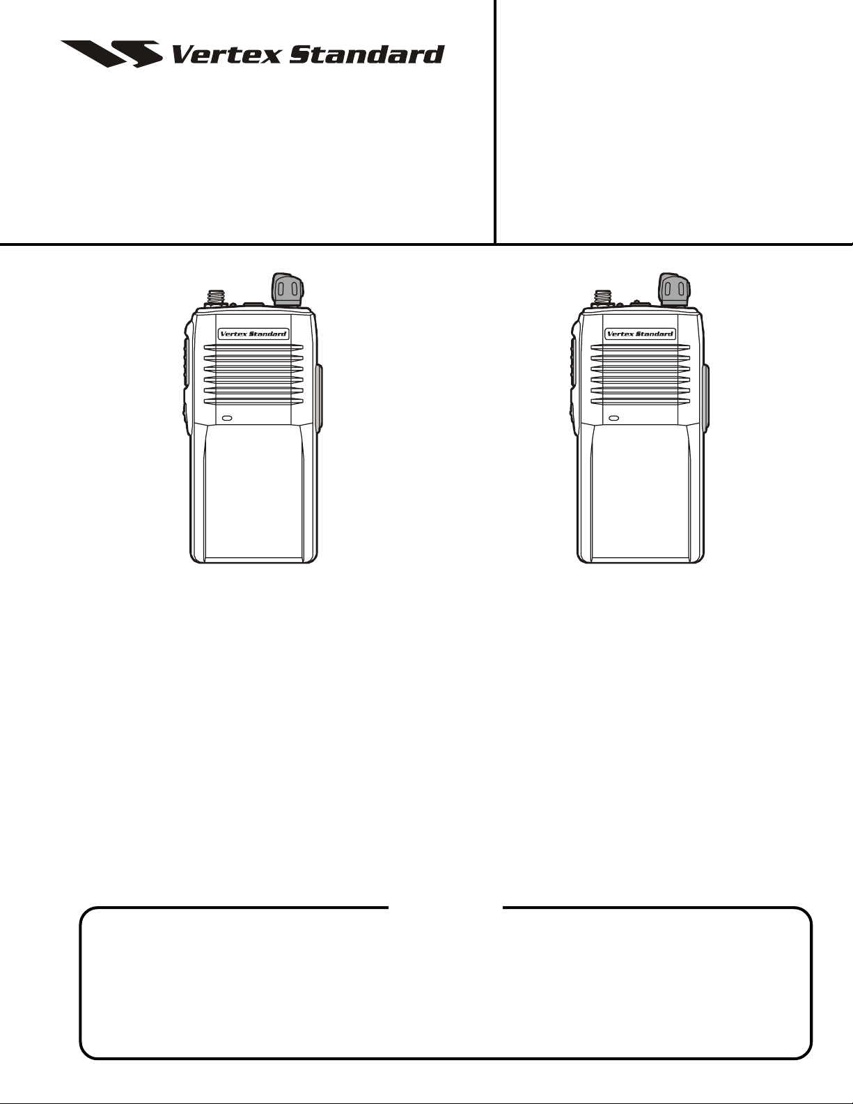
VX-131/-132
VHF Model
Service Manual
©2004 VERTEX STANDARD CO., LTD. EC059N90A
VERTEX STANDARD CO., LTD.
4-8-8 Nakameguro, Meguro-Ku, Tokyo 153-8644, Japan
VERTEX STANDARD
US Headquarters
10900 Walker Street, Cypress, CA 90630, U.S.A.
YAESU EUROPE B.V.
P.O. Box 75525, 1118 ZN Schiphol, The Netherlands
YAESU UK LTD.
Unit 12, Sun Valley Business Park, Winnall Close
Winchester, Hampshire, SO23 0LB, U.K.
VERTEX STANDARD HK LTD.
Unit 5, 20/F., Seaview Centre, 139-141 Hoi Bun Road,
Kwun Tong, Kowloon, Hong Kong
VX-131 VX-132
Introduction
This manual provides technical information necessary for servicing the VX-131 and VX-132 VHF FM Transceiver.
Servicing this equipment requires expertise in handling surface-mount chip components. Attempts by non-qualified
persons to service this equipment may result in permanent damage not covered by the warranty, and may be illegal in
some countries.
Two PCB layout diagrams are provided for each double-sided circuit board in the transceiver. Each side of is referred to
by the type of the majority of components installed on that side (“leaded” or “chip-only”). In most cases one side has only
chip components, and the other has either a mixture of both chip and leaded components (trimmers, coils, electrolytic
capacitors, ICs, etc.), or leaded components only.
While we believe the technical information in this manual to be correct, VERTEX STANDARD assumes no liability for
damage that may occur as a result of typographical or other errors that may be present. Your cooperation in pointing out
any inconsistencies in the technical information would be appreciated.
Contents
Specifications................................................... 2
Exploded View & Miscellaneous Parts ...... 3
Programming the Channel Data .................. 4
Cloning ............................................................. 6
Block Diagram ................................................. 7
Circuit Description ................................. 9
Alignment ............................................... 13
MAIN Unit
Circuit Diagram ....................................................... 21
Parts Layout ............................................................. 23
Parts List ...................................................................25
1
Page 2

Specifications
General
Frequency Range: 150 - 174 MHz
Number of Channels: 1 channel (VX-131),
2 channles (VX-132)
Channel Spacing: 12.5 / 25 kHz
Power Supply Voltage: 7.5 VDC ± 10%
Operating Temperature Range: –22 °F to +140 °F (–30 °C to +60 °C)
Frequency Stability: ±2.5 ppm
Dimensions (WHD): 2.3“ x 4.7“ x 1.2“ (58 x 120 x 31 mm)
Weight (approx.): 12.7 oz (360 g) w/FNB-64, antenna, and belt clip
Receiver (Measurements made per EIA standard TIA/EIA-603)
Circuit Type: Double-Conversion Superheterodyne
Intermediate Frequencies: 1st: 44.25 MHz,
2nd: 450 kHz
Sensitivity: 0.25 µV (EIA 12 dB SINAD)
0.35 µV (20 dB Quieting)
Selectivity (–6 dB /–60 dB): 12 kHz / 30 kHz (25 kHz),
9 kHz / 30 kHz (12.5 kHz)
Adjacent channel selectivity: 65 dB (25 kHz),
60 dB (12.5 kHz)
Intermodulation: 65 dB
Spurious and Image Rejection: 65 dB
Hum & Noise 45 dB
Audio output: 500 mW @4 Ohms, 10 % THD
Transmitter (Measurements made per EIA standard TIA/EIA-603)
Power output: 2.0 W
Modulation: 16K0F3E (25 kHz),
11K0F3E (12.5 kHz)
Conducted Spurious Emissions: 60 dB Below Carrier
FM Hum & Noise: 40 dB (25 kHz)
35 dB (12.5 kHz)
Audio distortion (@ 1 kHz): <5 %
Measurements per EIA standards unless noted above. Specifications subject to change without notice or obligation.
2
Page 3
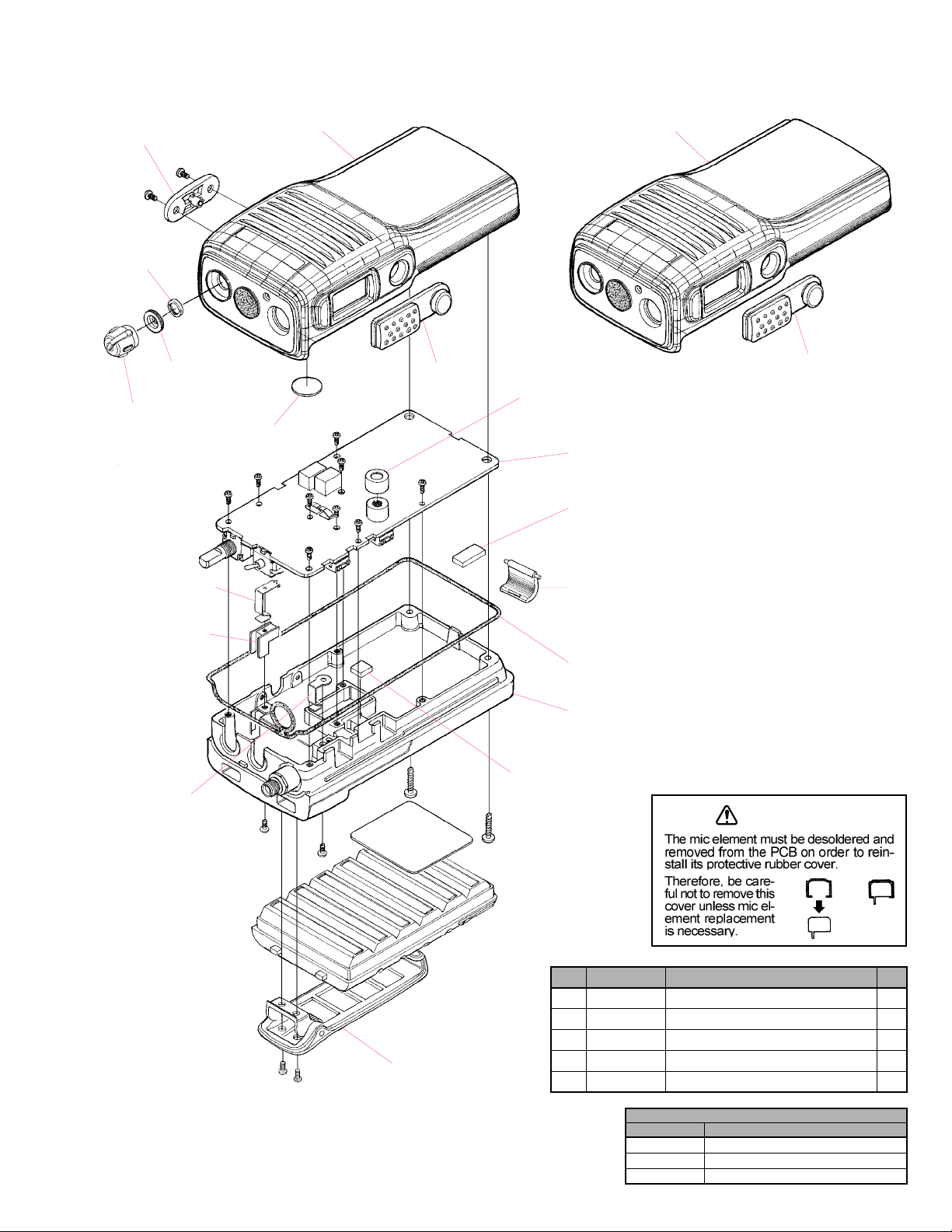
Exploded View & Miscellaneous Parts
RA0173500
CAP
R6147510
RING NUT
RA0296100
VOLUME KNOB
RA0631200
FRONT CASE ASSY (VX-132)
(w/PTT KNOB)
RA029430A
RUBBER PACKING
RA0309800
MYLAR SHEET (SP)
RA0631300
FRONT CASE ASSY (VX-131)
(w/PTT KNOB)
RA0294200
PTT KNOB
RA0110200
HOLDER RUBBER
RA0294200
PTT KNOB
CB2910001 (VX-131)
CB2910002 (VX-132)
MAIN UNIT
RA0623900
SPONGE RUBBER
RA0351700
TERMINAL PLATE (+)
RA010340B
TERMINAL HOLDER
RA0351600
TERMINAL PLATE (–)
RA0533600
SHEET (GP1-1.0-6X6)
CP8021001
BELT CLIP ASSY
Non-designated parts are available only as part of a designated assembly.
RA0123500
LATCH NAIL B
RA029430A
RUBBER PACKING
RA029310D
REAR CASE ASSY
(w/SMA CONNECTOR, TERMINAL PLATE L,
PAN HEAD SCREW M2X3NI)
CAUTION
REF. VXSTD P/N Description Qty.
U44104002 TAPTITE SCREW M2X4NI 10
U20206007 BINDING HEAD SCREW M2.6X6B 2
U24110002 TAPTITE SCREW M2X10NI 2
U02206007 SEMS SCREW SM2.6X6B 2
U00103002 PAN HEAD SCREW M2X3NI 1
ACCESSORIES
VXSTD P/N
AAA46X001
A14170002
AAE24X002
FNB-64 Ni-Cd Battery Pack
NC-77B Overnight Battery Charger
ATV-8B VHF Antenna
DESCRIPTION
3
Page 4
Programming the Channel Data
The VX-131/-132 transceiver allows you to change the channel frequency and its CTCSS/DCS status. Also, you may select
the channel bandwidth (wide/narrow) of all VHF frequencies and some UHF frequencies (see the channel table).
Programming the Operation Frequency
Turn the radio on while pressing and holding in the
PTT and MONITOR buttons.
Hold in the PTT and MONITOR buttons until the LED
indicator glows orange (approx. 3 seconds), then release the PTT and MONITOR buttons.
If your radio is the VX-132 (two channel model), toggle
the CH switch to the channel (“1” or “2”) on which
you want to program the new channel frequency.
Press the MONITOR button momentarily; the LED in-
dicator will change to red and the radio will emit a
“channel confirmation beep” that describes the current channel programming, according to the following rule.
)
FIRST AND SECOND BEEPS (LOW PITCH TONES
NUMBER
BANDWIDTH
Wide
CONFIRMATION BEEP
–––
0
1
2
3
4
(two seconds
THIRD BEEPS (HIGH PITCH TONES
CONFIRMATION BEEPBANDWIDTH
)
NUMBER
5
6
7
8
9
Narrow
Examples:
Channel Number 6, Bandwidth “Wide”:
––– –
0 6 Wide
Channel Number 18, Bandwidth “Narrow”:
1 8 Narrow
–
Press the PTT button once each for each quantity of
“ten” in the channel number (i.e. press PTT three times
for channel 3n); when finished entering the “tens”
place, a confirmation beep will be heard. Immediately
after the confirmation beep, press the PTT button once
each to complete the “ones” in the channel number
(i.e. press PTT twice for channel 32, after receiving
the first confirmation beep). Now press the PTT button once or twice, corresponding to the bandwidth
(once for “Narrow” or twice for “Wide”). When entry
is complete, the radio will emit a confirmation beep.
In this programming sequence, if you wish to enter
the number “0,” press and hold in the PTT button until
the channel confirmation beep (long tone) is heard. If
the channel is a “Narrow-only” channel (such as UHF
channel “03”), you do not need to enter the bandwidth.
Examples:
Channel Number 6, Bandwidth “Wide”:
–––
0 6 Wide
Channel Number 18, Bandwidth “Narrow”:
1 8 Narrow
: C
HANNEL
CONFIRMATION BEEP
–
–
–
–
)
: B
ANDWIDTH
CONFIRMATION BEEP
If the channel programming process fails, the radio
will emit an alert tone (beep-beep-beep:
).
You may check the channel number by pressing the
MONITOR button. The radio will respond with the
channel programming confirmation beeps according
to the chart at the beginning of this section.
Programming the CTCSS/DCS/ARTS Status
Turn the radio on while pressing and holding in the
PTT and MONITOR buttons.
Hold in the PTT and MONITOR buttons until the LED
indicator glows orange (approx. 3 seconds), then release the PTT and MONITOR buttons.
If your radio is the VX-132 (two channel model), toggle
the CH switch to the desired channel (“1” or “2”) on
which you want to program the CTCSS/DCS tone or
ARTS Operation.
Press and hold in the MONITOR button for 2 seconds;
the LED indicator will change to green, and the radio
will emit a CTCSS/DCS/ARTS status confirmation
beep that describes the current CTCSS/DCS/ARTS status, according to the following rule (see also the
CTCSS/DCS/ARTS Chart):
CTCSS/DCS/ARTS STATUS NUMBER
NUMBER
Examples:
CTCSS/DCS “OFF” (000):
CTCSS “88.5 Hz” (Tone 009 per CTCSS/DCS Chart):
DCS “023” (Tone 051 per CTCSS/DCS/ARTS Chart):
Press the PTT button once each for each quantity of
100 in the CTCSS/DCS/ARTS status code, per the
CTCSS/DCS/ARTS Chart; as before, when entry is
completed for the “100s” place, the radio will emit a
confirmation beep. Now press the PTT button once
each for each quantity of tens in the CTCSS/DCS/ARTS
status code number, get the confirmation beep, then
press the PTT button once each to set the “ones” place,
after which the final confirmation beep will be heard.
In this entry sequence, to enter the number “0,” press
and hold in the PTT button until the channel confirmation beep (long tone) is heard.
0
1
2
3
4
CONFIRMATION BEEP
–––
(two seconds
)
NUMBER
5
6
7
8
9
––– ––– –––
000
––– ––– –
009
–––
05 1
CONFIRMATION BEEP
–
–
–
–
4
Page 5
Examples:
Enter the CTCSS “88.5 Hz” (009):
––– –––
009
Enter the DCS code “023” (051)
–––
05 1
Activate ARTS using DCS code “165” (163):
16 3
If the CTCSS/DCS/ARTS status programming process
fails, the radio will emit an alert tone (beep-beep-beep:
).
You may check the CTCSS/DCS/ARTS status by press-
ing and holding in the MONITOR button. The radio
will respond with the CTCSS/DCS confirmation beeps
according to the chart at the beginning of this section.
Programming the Channel Data
CH
1
2
CH
01
02
03
04
05
06
07
08
09
10
Code #
001
002
003
004
005
006
007
008
009
010
011
012
013
014
015
016
017
018
019
020
021
022
023
024
025
VX-131 DEFALUT SETTING
Frequency
(
MHz
151.6250
–
Frequency
(
MHz
151.6250
151.9550
154.5700
154.6000
151.7000
151.7600
151.5125
151.6550
151.6850
151.7150
)
)
W/N
W/N
W/N
W/N
W/N
W/N
W/N
W/N
W/N
W/N
CTCSS
67.0 Hz
69.3 Hz
71.9 Hz
74.4 Hz
77.0 Hz
79.7 Hz
82.5 Hz
85.4 Hz
88.5 Hz
91.5 Hz
94.8 Hz
97.4 Hz
100.0 Hz
103.5 Hz
107.2 Hz
110.9 Hz
114.8 Hz
118.8 Hz
123.0 Hz
127.3 Hz
131.8 Hz
136.5 Hz
141.3 Hz
146.2 Hz
151.4 Hz
BW
W
BW
channels are non-EIA/TIA standard codes
CTCSS/
DCS
OFF
–
–
VHF MODEL CHANNEL CHART
Red
Blue
–
–
–
–
–
–
CH
11
12
13
14
15
16
17
18
19
20
CTCSS
156.7 Hz
159.8 Hz
162.2 Hz
165.5 Hz
167.9 Hz
171.3 Hz
173.8 Hz
177.3 Hz
179.9 Hz
183.5 Hz
186.2 Hz
189.9 Hz
192.8 Hz
196.6 Hz
199.5 Hz
203.5 Hz
206.5 Hz
210.7 Hz
218.1 Hz
225.7 Hz
229.1 Hz
233.6 Hz
241.8 Hz
250.3 Hz
254.1 Hz
Color
Purple
Green
Code #
026
027
028
029
030
031
032
033
034
035
036
037
038
039
040
041
042
043
044
045
046
047
048
049
050
VX-132 DEFALUT SETTING
Frequency
(
MHz
151.6250
151.9550
Frequency
(
151.7450
151.7750
151.8650
151.8950
151.9250
152.7000
154.4900
154.5150
154.5400
154.6000
MHz
)
)
Code #
051
052
053
054
055
056
057
058
059
060
061
062
063
064
065
066
067
068
069
070
071
072
073
074
075
BW
W
W
BW
W/N
W/N
W/N
W/N
W/N
W/N
W/N
W/N
W/N
W/N
CTCSS/
DCS
OFF
OFF
Frequency
CH
(
MHz
21
154.6550
22
158.4000
–
–
–
–
–
–
–
–
CTCSS/DCS/ARTS STATUS CODE CHART
DCS
023
025
026
030
032
036
043
047
051
053
054
065
071
072
073
074
114
115
116
122
125
131
132
134
143
)
–
–
–
–
–
–
–
–
Code #
076
077
078
079
080
081
082
083
084
085
086
087
088
089
090
091
092
093
094
095
096
097
098
099
100
BW
W/N
W/N
–
–
–
–
–
–
–
–
DCS
145
152
155
156
162
165
172
174
205
212
223
224
225
226
243
244
245
246
250
251
252
255
261
263
265
Code #
101
102
103
104
105
106
107
108
109
110
111
112
113
114
115
116
117
118
119
120
121
122
123
124
125
DCS
266
271
274
306
311
315
325
331
332
343
346
351
356
364
365
371
411
412
413
423
431
432
435
445
446
Code #
126
127
128
129
130
131
132
133
134
135
136
137
138
139
140
141
142
143
144
145
146
147
148
149
150
DCS
452
454
455
462
464
465
466
503
506
516
523
526
532
546
565
606
612
624
627
631
632
654
662
664
703
Code #
151
152
153
154
155
156
157
158
159
160
161
162
163
164
165
166
167
168
169
170
171
172
173
174
000
DCS
712
723
731
732
734
743
754
ARTS (023)
ARTS (043)
ARTS (071)
ARTS (116)
ARTS (143)
ARTS (165)
ARTS (224)
ARTS (246)
ARTS (263)
ARTS (311)
ARTS (346)
ARTS (411)
ARTS (435)
ARTS (462)
ARTS (516)
ARTS (606)
ARTS (654)
OFF
5
Page 6
Cloning
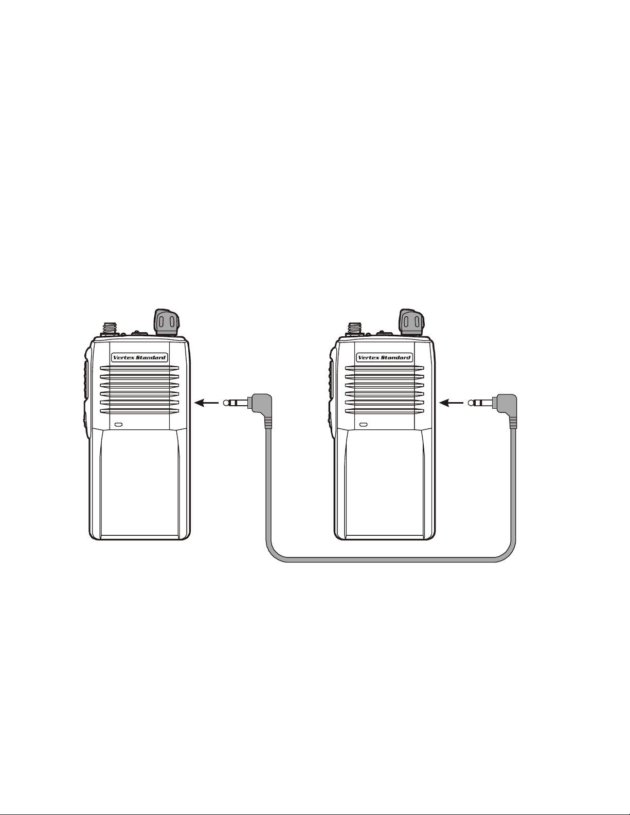
The VX-131/-132 series includes a convenient “Cloning” feature, which allows the programming data from one transceiver to be transferred to another VX-131/-132 series. Here is the procedure for cloning one radio’s data to another.
1. Turn both transceiver off.
2. Remove the plastic cap and its two mounting screws
from the MIC/SP jack on the right side of the transceiver. Do this for both transceivers
3. Connect the optional CT-27 cloning cable between the
MIC/SP jacks of the two transceivers.
4. Turn the radio on while pressing and holding in the
MONITOR button.
5. Hold in the MONITOR button until the LED indicator
blinks orange (approx. 5 seconds), the release the
MONITOR button. Do this for both transceiver (the
order of the switch-on does not matter).
6. On the Destination transceiver, press the MONITOR
button. The LED indicator will change to green.
7. Press the PTT button on the Source transceiver, the
LED indicator will change to red, and the data will be
transferred.
8. If there is a problem during the cloning process, the
LED indicator will blink green; check your cable connections and battery voltage, and try again.
9. If the data transfer is successful, the LED indicator
return to blinking orange. Turn both transceivers off
and disconnect CT-27 cable. You can then turn the
transceivers back on, and begin normal operation.
10. Replace the plastic cap and its two mounting screws.
Optional Cloning Cable CT-27
6
Page 7
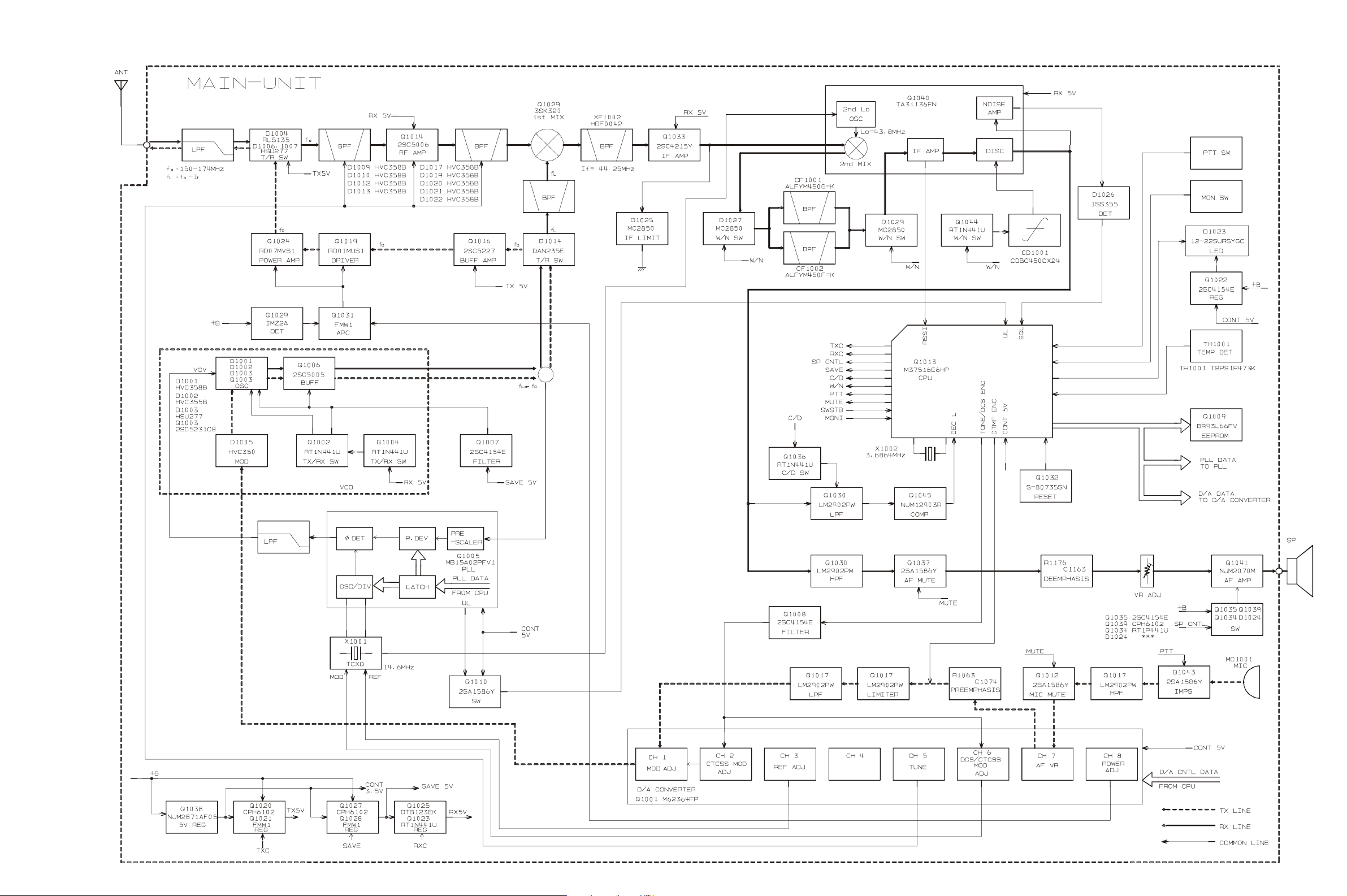
Block Diagram
7
Page 8

Block Diagram
Note
8
Page 9

Circuit Description
Receive Signal Path
Incoming RF signal from the antenna jack is delivered to
the MAIN Unit and passes through a low-pass filter consisting of coils L1003 and L1006, capacitors C1009, C1012,
C1020, C1023, and C1030, and antenna switching diodes
D1006 and D1007 (both HSU277).
Signals within the frequency range of the transceiver enter a varactor-tuned band-pass filter consisting of coils
L1011 and L1012, capacitors C1062, C1064, C1075, C1081,
and C1084, and diodes D1009, D1010, D1012, and D1013
(all HVC355B), then amplified by RF amplifier Q1014
(2SC5006) and enter a varactor-tuned band-pass filter consisting of coils L1019 and L1021, capacitors C1096, C1099,
C1108, and C1113, and diodes D1019, D1020, D1021, and
D1022 (all HVC355B), before 1st mixing by 1st mixer
Q1026 (3SK320).
Buffered output from the VCO Q1003 (2SC5231) is am-
plified by Q1006 (2SC5005) to provide a pure 1st local
signal between 194.25 and 218.25 MHz for injection to the
1st mixer Q1026 (3SK320). The 44.25 MHz 1st IF signal
then passes through monolithic crystal filter XF1002 to
strip away all but the desired signal. The filtered 1st IF
signal is amplified by Q1033 (2SC4215Y).
The amplified 1st IF signal is applied to FM IF subsystem
IC Q1040 (TA31136FN), which contains the 2nd mixer,
2nd local oscillator, limiter amplifier, noise amplifier, and
RSSI amplifier.
A 2nd local signal is produced from the PLL reference/
2nd local oscillator of 14.60 MHz crystal X1001. The 14.60
MHz reference signal is tripled by Q1040 (TA31136FN),
capacitor C1173, and coil L1030, then resulting the 43.8
MHz second local signal delivered to mixer section of
Q1040 (TA31136FN) which produce the 450 kHz 2nd IF
mixed with the 1st IF signal.
The 2nd IF signal passes through the ceramic filter CF1001
(for “Narrow” bandwidth channels) or CF1002 (for
“Wide” bandwidth channels) to strip away unwanted
mixer products, and is then applied to the limiter amplifier in Q1040 (TA31136FN), which removes amplitude vari-
ations in the 450kHz IF, before detection of the speech by
the ceramic discriminator CD1001.
Detected audio from CD1001 is applied to the audio highpass filter Q1030 (LM2902PW), and then passes through
the AF mute switch Q1037 (2SA1586Y), de-emphasis cir-
cuit consisting of resistor R1176 and Capacitor C1136, and
volume control to the audio amplifier Q1041 (NJM2070M),
which provides up to 0.5 Watts to the internal 4-Ω loudspeaker or the optional headphone.
Squelch Control
The squelch circuitry consists of a noise amplifier and
band-pass filter within Q1040 (TA31136FN) and noise
detector D1026 (1SS355).
When no carrier received, noise at the output of the detector stage in Q1040 (TA31136FN) is amplified and band-
pass filtered by the noise amplifier section of Q1040
(TA31136FN) and the network between pins 7 and 8 of
Q1040 (TA31136FN), and then rectified by D1026
(1SS355).
The resulting DC squelch control voltage is passed to pin
37 of the microprocessor Q1013 (M37516F8HP). If no car-
rier is received, this signal causes pin 20 and 24 of Q1013
(M37516F8HP) to go high. Pin 24 signal disable the supply voltage of the audio amplifier Q1041 (NJM2070M).
Thus, the microprocessor blocks output from the audio
amplifier, and silences the receiver while no signal is being received (and during transmission, as well). Pin 20
signal hold the green (Busy) half of the LED D1023 (12-
22SURSYGC) to off.
When a carrier appears at the discriminator, noise is removed from the receiver output, causing pin 37 of Q1013
(M37516F8HP) to go low and the microprocessor to activate the green (Busy) half of the LED D1023 (12-
22SURSYGC) via Q1013 (M37516F8HP).
The microprocessor Q1013 (M37516F8HP) checks for the
CTCSS or DCS code squelch information. If the CTCSS or
DCS is not activated, or the received tone or code matches
that programmed, allows audio to pass through the audio amplifier Q1041 (NJM2070M) to the loudspeaker by
enabling the supply voltage to it via Q1039 (CPH6102).
Transmit Signal Path
Speech input from the microphone passes through a highpass filter Q1017 (LM2902PW-2) and AF mute switch
Q1012 (2SA1586Y) to Q1001 (M62364FP) which adjust
the microphone gain. The adjusted audio passes through
a pre-emphasis circuit consisting of resistor R1063 and Capacitor C1074 to the limiter amplifier Q1017 (LM2902PW-
3). The limited audio is applied to a low-pass filter Q1017
(LM2902PW-1/-4), then return to Q1001 (M62364FP)
which adjust the deviation level.
The audio signal is applied to varactor diode D1005
(HVC350) which which frequency modulates the VCO
Q1003 (2SC5231). The modulated signal from the VCO
Q1003 (2SC5231) is buffered by Q1006 (2SC5005), then
passes through the T/R switching diode D1014 (DAN235E)
to the driver amplifier Q1016 (2SC5227) and Q1019
(RD01MUS1), then amplified transmit signal is applied
to the final amplifier Q1024 (RD07MVS1) up to 2 watts
output power.
9
Page 10

Circuit Description
The transmit signal then passes through the antenna switch
D1004 (RLS135) and is low-pass filtered to suppress har-
monic spurious radiation before delivery to the antenna.
CTCSS/DCS Signal Path
If a CTCSS tone encoder is enabled, the CTCSS tone generated by Q1013 (M37516F8HP), then delivered to VCO
Q1003 (2SC5231) and TCXO X1001 for CTCSS modulating.
If a DCS encoder is enabled, the DCS code is generated by
microprocessor Q1013 (M37516F8HP), then delivered to
TCXO X1001 for DCS modulating.
Automatic Transmit Power Control
Current from the final amplifier is sampled by R1136,
R1139 and R1142, and is rectified by Q1029 (IMZ2A). The
resulting DC is fed through the Automatic Power Controller Q1031 (FMW1) to the drive amplifier Q1019
(RD01MUS1) and final amplifier Q1024 (RD07MVS1), for
control of the power output.
Transmit Inhibit
When the transmit PLL is unlocked, pin 7 of PLL IC Q1005
(MB15A02PFV1) goes to logic “Low”, and unlock detector Q1010 (2SA1586) goes to logic “High”. The resulting
DC unlock control voltage is passed to pin 14 of the microprocessor Q1013 (M37516F8HP). While the transmit
PLL is unlocked, pin 22 of Q1013 (M37516F8HP) remains
high, which turns off Q1020 (CPH6102) and the Automatic Power Controller Q1031 (FMW1) to disable the supply voltage to the drive amplifier Q1019 (RD01MUS1) and
final amplifier Q1024 (RD07MVS1), thereby disabling the
transmitter.
PLL Frequency Synthesizer
The PLL circuitry on the Main Unit consists of VCO Q1003
(2SC5231), VCO buffer Q1006 (2SC5005), and PLL IC
Q1005 (MB15A02PFV1) which contains a reference divid-
er, serial-to-parallel data latch, programmable divider,
phase comparator and charge pump.
While receiving, VCO Q1003 (2SC5231) oscillates be-
tween 194.25 and 218.25 MHz according to the programmed receiving frequency. The VCO output is buffered by Q1006 (2SC5005), then applied to the prescaler
section of Q1005 (MB15A02PFV1). There the VCO signal
is divided by 64 or 65, according to a control signal from
the data latch section of Q1005 (MB15A02PFV1), before
being sent to the programmable divider section of Q1005
(MB15A02PFV1).
The data latch section of Q1005 (MB15A02PFV1) also re-
ceives serial dividing data from the microprocessor Q1013
(M37516F8HP), which causes the pre-divided VCO signal to be further divided in the programmable divider
section, depending upon the desired receive frequency,
so as to produce a 2.5 kHz, 5 kHz, or 6.25 kHz derivative
of the current VCO frequency.
Meanwhile, the reference dividers section of Q1005 divides 14.60 MHz reference frequency from the TCXO Unit
X1001, by 5840 (or 2920 or 2336) to produce the 2.5 kHz
(or 5 kHz or 6.25 kHz) loops reference (respectively).
The 2.5 kHz (or 5 kHz or 6.25 kHz) signal from the programmable divider (derived from the VCO) and that derived from the reference oscillator are applied to the phase
detector section of Q1005 (MB15A02PFV1), which pro-
duces a pulsed output with pulse duration depending on
the phase difference between the input signals.
Spurious Suppression
Generation of spurious products by the transmitter is minimized by the fundamental carrier frequency being equal
to final transmitting frequency, modulated directly in the
transmit VCO. Additional harmonic suppression is provided by a low-pass filter consisting of coils L1003 and
L1006, capacitors C1009, C1012, C1020, C1023, and C1030,
resulting in more than 60 dB of harmonic suppression
prior to delivery to the antenna.
10
This pulse train is filtered to DC and returned to the varactor diodes D1001 (HVC358B) and D1002 (HVC355B).
Changes in the level of the DC voltage applied to the varactor diodes, affecting the reference in the tank circuit of
the VCO according to the phase difference between the
signals derived from the VCO and the TCXO Unit X1001.
The VCO is thus phase-locked to the crystal reference oscillator. The output of the VCO Q1003 (2SC5231), after
buffering by Q1006 (2SC5005), is applied to the 1st mixer
as described previously.
For transmission, the VCO Q1003 (2SC5231) oscillates
between 150 and 174 MHz according to the programmed
transmit frequency. The remainder of the PLL circuitry is
shared with the receiver. However, the dividing data from
the microprocessor is such that the VCO frequency is at
the actual transmit frequency (rather than offset for IFs,
as in the receiving case). Also, the VCO is modulated by
the speech audio applied to D1005 (HVC350), as described
previously.
Page 11

Receive and transmit buses select which VCO is made
active by Q1002 and Q1004 (both RT1N441U). TCXO unit
X1001 yields frequency stability of ±2.5 ppm @ –30 °C to
+60 °C.
Push-To-Talk Transmit Activation
The PTT switch S1002 is connected to pin 48 of microprocessor Q1013 (M37516F8HP), so that when the PTT switch
is closed, pin 23 of Q1013 (M37516F8HP) goes low. This
signal disables the receiver by disabling the 5 V supply
bus at Q1025 (DTB123EK) to the front-end, FM IF subsystem IC Q1040 (TA31136FN), and receiver VCO circuit-
ry.
At the same time, pin 22 of Q1013 (M37516F8HP) goes
high to activates the transmit 5V supply line at Q1021
(FMW1) and Q1020 (CPH6102) to enable the transmitter.
Circuit Description
11
Page 12

Circuit Description
Note13Introduction
12
Page 13

The VX-131/-132 has been aligned at the factory for the
specified performance across the entire frequency range
specified. Realignment should therefore not be necessary
except in the event of a component failure. All component replacement and service should be performed only
by an authorized Vertex Standard representative, or the
warranty policy may be voided.
The following procedures cover the sometimes critical and
tedious adjustments that are not normally required once
the transceiver has left the factory. However, if damage
occurs and some parts are replaced, realignment may be
required. If a sudden problem occurs during normal operation, it is likely due to component failure; realignment
should not be done until after the faulty component has
been replaced.
We recommend that servicing be performed only by authorized Vertex Standard service technicians who are experienced with the circuitry and fully equipped for repair
and alignment. Therefore, if a fault is suspected, contact
the dealer from whom the transceiver was purchased for
instructions regarding repair. Authorized Vertex Standard
service technicians realign all circuits and make complete
performance checks to ensure compliance with factory
specifications after replacing any faulty components.
Those who do undertake any of the following alignments
are cautioned to proceed at their own risk. Problems
caused by unauthorized attempts at realignment are not
covered by the warranty policy. Also, Vertex Standard
must reserve the right to change circuits and alignment
procedures in the interest of improved performance, without notifying owners. Under no circumstances should any
alignment be attempted unless the normal function and
operation of the transceiver are clearly understood, the
cause of the malfunction has been clearly pinpointed and
any faulty components replaced, and the need for realignment determined to be absolutely necessary. The following test equipment (and thorough familiarity with its correct use) is necessary for complete realignment. Correction of problems caused by misalignment resulting from
use of improper test equipment is not covered under the
warranty policy. While most steps do not require all of
the equipment listed, the interactions of some adjustments
may require that more complex adjustments be performed
afterwards. Do not attempt to perform only a single step
unless it is clearly isolated electrically from all other steps.
Have all test equipment ready before beginning, and follow all of the steps in a section in the order presented.
Alignment
Required Test Equipment
Radio Tester with calibrated output level at 500 MHz
In-line Wattmeter with 5 % accuracy at 500 MHz
50-ohm, 10-W RF Dummy Load
Regulated DC Power Supply (standard 7.5V DC, 3A)
Frequency Counter: ±0.2 ppm accuracy at 500 MHz
AF Signal Generator
VHF Sampling Coupler
IBM PC/compatible Computer with Microsoft® Win-
dows95® or later operating system
Vertex Standard CT-42A or FIF-10/CT-106 Program-
ming Cable and CE74 Programming Software
Alignment Preparation & Precautions
A 50-ohm RF Dummy load and in-line wattmeter must be
connected to the antenna jack in all procedures that call
for transmission, except where specified otherwise. Correct alignment is not possible with an antenna.
After completing one step, read the following step to determine whether the same test equipment will be required.
If not, remove the test equipment (except dummy load
and wattmeter, if connected) before proceeding.
Correct alignment requires that the ambient temperature
be the same as that of the transceiver and test equipment,
and that this temperature be held constant between 68 °F
and 86 °F (20 °C ~ 30 °C). When the transceiver is brought
into the shop from hot or cold air, it should be allowed
time to come to room temperature before alignment.
Whenever possible, alignments should be made with oscillator shields and circuit boards firmly affixed in place.
Also, the test equipment must be thoroughly warmed up
before beginning.
Note: Signal levels in dB referred to in this procedure are
based on 0 dBµ = 0.5 µV (closed circuit).
Important Note
When connecting the Programming Cable into the
MIC/SP jack of the VX-131/-132, you must remove the
plastic cap and its mounting screws prior to programming. Please remember to re-attach the cap and screws
when the programming is complete.
Page 14

Alignment
Set up the test equipment
Set up the test equipment as shown below for transceiver
alignment, and apply 7.5V DC power to the transceiver.
In-Line
Wattmeter
50-ohm RF
Dummy Load
Deviation
Meter
Frequency
Counter
Regulated
7.5 VDC P.S.
RF Signal
Generator
4-ohm AF
Dummy Load
SINAD Meter
AF Signal
Generator
Data Input/Output
AF Signal Input
AF Signal Output
The Alignment Tool Outline
Basic Alignment Sequence
1. Activates the CE74 Programming Software.
2. Upload the Current Channel Data of the radio, then
save to the disk.
3. Open the Alignment Channel Data (test-v.C74), then
download to the transceiver.
4. Enter the Alignment Mode.
5. Align the data.
6. Download the Align Data to the transceiver.
7. Open the Current Channel Data which is stored in step
2, then download to the transceiver.
8. Alignment is now completely. Close the CE74 Pro-
gramming Software.
Menu of the Tool
RF Frequency
Set the transceiver to “CH 2 (160.005 MHz)“ via the
“CH” box.
Double click the left mouse button on the “RF Fre-
quency
Move the Slide bar, as need, so that the frequency
counter reading is 160.0050 MHz (± 100 Hz).
Click the left mouse button on the [OK] box to lock in
the new data.
” parameter to open the pop-up window.
14
Page 15

Alignment
Transmitter Output Power
Set the transceiver to “CH 2 (160.005 MHz)“ via the
“CH” box.
Double click the left mouse button on the “RF Power
” parameter to open the pop-up window.
(2W)
MAX Deviation
Set the transceiver to “CH 2 (160.005 MHz)“ via the
“CH” box.
Inject a 1 kHz tone at –17 dBm to the MIC jack.
Double click the left mouse button on the “MAX De-
” parameter to open the pop-up window.
viation
Move the Slide bar, as need, so that the power meter
reading is 2.0 W (± 0.1 W).
Click the left mouse button on the [OK] box to lock in
the new data.
Move the Slide bar, as need, so that the deviation meter
reading is ±4.2 kHz (± 0.1 kHz) deviation.
Click the left mouse button on the [OK] box to lock in
the new data.
15
Page 16

Alignment
MIC Sensitivity
Set the transceiver to “CH 2 (160.005 MHz)“ via the
“CH” box.
Inject a 1 kHz tone at –37 dBm to the MIC jack.
Double click the left mouse button on the “MIC Sen-
” parameter to open the pop-up window.
sitivity
CTCSS VCO Modulation
Set the transceiver to “CH 2 (160.005 MHz)“ via the
“CH” box.
Activate the CTCSS encoder with “254.1 Hz“ Tone via
the “SUB AUDIO”parameter.
Set the “CTCSS Ref. Modulation” parameter to “0.“
Double click the left mouse button on the “CTCSS VCO
Modulation
” parameter to open the pop-up window.
Move the Slide bar, as need, so that the deviation meter
reading is ±3.0 kHz (± 0.1 kHz) deviation.
Click the the left mouse button on the [OK] box to lock
in the new data.
Move the Slide bar, as need, so that the deviation meter
reading is ±0.9 kHz (± 0.1 kHz) deviation.
Click the the left mouse button on the [OK] box to lock
in the new data.
16
Page 17

Alignment
CTCSS Ref. Modulation
Set the transceiver to “CH 2 (160.005 MHz)“ via the
“CH” box.
Activate the CTCSS encoder with “67.0 Hz“ Tone via
the “SUB AUDIO”parameter.
Double click the left mouse button on the “CTCSS Ref.
Modulation
” parameter to open the pop-up window.
DCS Deviation
Set the transceiver to “CH 2 (160.005 MHz)“ via the
“CH” box.
Activate the DCS encoder with “627“ Tone Code via
the “SUB AUDIO”parameter.
Double click the left mouse button on the “DCS De-
” parameter to open the pop-up window.
viation
Move the Slide bar, as need, so that the deviation meter
reading is ±0.8 kHz (± 0.1 kHz) deviation.
Click the the left mouse button on the [OK] box to lock
in the new data.
Move the Slide bar, as need, so that the deviation meter
reading is ±0.75 kHz (± 0.1 kHz) deviation.
Click the the left mouse button on the [OK] box to lock
in the new data.
17
Page 18

Alignment
RX Sensitivity
Set the transceiver to “CH 3 (173.995 MHz)“ via the
“CH” box.
Injust a 160.005 MHz siganl at a level of 40dBµ with
±3.0 kHz deviation with a 1 kHz to the Antenna Jack.
Double click the left mouse button on the “RX Sensi-
” parameter to open the pop-up window.
tivity
Threshold NSQ Level (Wide)
Set the transceiver to “CH 2 (160.005 MHz/Wide)“ via
the “CH” box.
Injust a 160.005 MHz siganl at a level of –10dBµ with
±3.0 kHz deviation with a 1 kHz to the Antenna Jack.
Double click the left mouse button on the “Threshold
NSQ Level
” parameter to open the pop-up window.
Move the Slide bar, as need, to tune for best sensitiv-
ity; ultimately, the transceiver should be aligned so
that the RF Signal Generator output level is –6 dBµ
EMF (0.25 µV) or less for 12 dB SINAD.
Click the the left mouse button on the [OK] box to lock
in the new data.
Move the Slide bar from the Value “0” position to the
position which the LED indicator on the transceiver's
top panel will blinks green.
Click the the left mouse button on the [OK] box to lock
in the new data.
18
Page 19

Threshold NSQ Level (Narrow)
Set the transceiver to “CH 5 (160.005 MHz/Narrow)“
via the “CH” box.
Injust a 160.005 MHz siganl at a level of –10dBµ with
±1.5 kHz deviation with a 1 kHz to the Antenna Jack.
Double click the left mouse button on the “Threshold
NSQ Level
” parameter to open the pop-up window.
Alignment
Move the Slide bar from the Value “0” position to the
position which the LED indicator on the transceiver's
top panel will blinks green.
Click the the left mouse button on the [OK] box to lock
in the new data.
This completes the Alignment routine, click the the left
mouse button on the [OK] box to save all settings and extit
from alignment mode.
19
Page 20

Alignment
Note
20
Page 21

5.0 V
MAIN Unit
Circuit Diagram
RX: 0 V
TX: 4.2 V
RX: 4.2 V
TX: 0 V
2.8 V
RX: 5.0 V
TX: 0 V
2.2 V
3.9 V
2.9 V
0.8 V
4.2 V
4.9 V
3.0 V
5.0 V
RX: 0 V
TX: 3.5 V
0.7 V
RX: 3.5 V
TX: 0 V
RX: 0 V
TX: 1.0 V
RX: 0 V
TX: 0.3 V
2.6 V
RX: 0 V
TX: 3.7 V
TX (2 W): 1.7 V
CH 1: 4.9 V
CH 2: 0 V
TX (2 W): 1.7 V
4.9 V
1.0 V
TX (2 W): 1.6 V
0.7 V
TX (2 W): 1.7 V
1.9 V
W: 3.1 V
N: 1.9 V
W: 3.7 V
N: 0 V
W: 5.0 V
N: 1.2 V
W: 3.7 V
N: 0 V
W: 3.1 V
N: 1.9 V
W: 5.0 V
N: 0 V
5.0 V
5.0 V
3.0 V
5.0 V
3.5 V
1.5 V
2.2 V (@25 °C)
RX: 0 V
TX: 5.0 V
GREEN "ON": 0 V
GREEN "OFF": 5.0 V
RED "ON": 0 V
RED "OFF": 5.0 V
RX: 5.0 V
TX: 0 V
4.3 V
5.0 V
7.5 V
SQL "CLOSE": 5.0 V
SQL "OPEN": 0.6 V
RX: 5.0 V
TX: 0 V
5.0 V
MUTE "ON": 5.0 V
MUTE "OFF": 0 V
5.0 V
MUTE "ON": 5.0 V
MUTE "OFF": 1.0 V
SQL "CLOSE": 0.2 V
SQL "OPEN": 7.4 V
SQL "CLOSE": 0.9 V
SQL "OPEN": 0.6 V
5.0 V
5.0 V
5.0 V
5.0 V
PTT "ON": 4.8 V
PTT "OFF": 0 V
PTT "ON": 0 V
PTT "OFF": 5.0 V
7.5 V
RX: 0 V
TX: 5.0 V
5.0 V
RX: 5.0 V
TX: 4.4 V
RX: 5.0 V
TX: 0 V
RX SAVE "OFF": 5.0 V
RX SAVE "OFF": 5.0 V
RX SAVE "OFF": 4.4 V
RX SAVE "OFF": 0 V
RX SAVE "OFF": 5.0 V
21
Page 22

MAIN Unit
Note
22
Page 23

MAIN Unit
Parts Layout (Side A)
A B C D E F G H
1
2
3
4
LM2902PWR
(Q1017, 1030)
NJM2070M
(Q1041)
2SA1586Y (SY)
(Q1012, 1037,
1043)
CPH6102 (AB)
(Q1039)
IMZ2 (Z2)
(Q1029)
RT1N441U (N3)
(Q1036)
12-22SURSYGC/S530-A2/TR8
(D1023)
NJM12903R
(Q1045)
2SC4154E (LE)
(Q1022, 1035)
FMW1 (W1)
(Q1031)
RD07MVS1
(Q1024)
RT1P441U (P3)
(Q1034)
MC2850 (A7)
(D1028)
23
Page 24

MAIN Unit
Parts Layout (Side B)
a
b
c
d
e
f
g
h
1
2
3
4
M37516F8HP
(Q1013)
M62364FP
(Q1001)
MB15A02PFV1
(Q1005)
TA31136FN
(Q1040)
BR93L66FV
(Q1009)
3SK320 (U7)
(Q1026)
RD01MUS1
(Q1019)
2SA1586Y (SY)
(Q1010)
2SC4154E (LE)
(Q1007, 1008)
2SC4215Y (QY)
(Q1033)
2SC5005 (73)
(Q1006)
2SC5006 (24)
(Q1014)
2SC5227 (LN)
(Q1016)
2SC5231 (C9)
(Q1003)
CPH6102 (AB)
(Q1020, 1027)
DTB123EK (F12)
(Q1025)
FMW1 (W1)
(Q1021, 1028)
NJM2871AF05 (82)
(Q1038)
RT1N441U (N3)
(Q1004, 1023,
1044)
RT1P441U (P3)
(Q1002, 1015)
S-80835CNMC
(Q1032)
DAN235E (M)
(D1014)
MC2850 (A7)
(D1015, 1025,
1027, 1029)
24
Page 25

MAIN Unit
Parts List
REF DESCRIPTION VALUE V/W TOL. MFR'S DESIG VXSTD P/N VERS.
PCB with Components CB2910001 1 CH
CB2910002 2 CH
Printed Circuit Board AC059N000 FR0120800 1C 1001 CHIP TA.CAP. 0.1uF 35V TESVA1V104M1-8R K78160025 1- B f4
C 1005 CHIP CAP. 2.2uF 10V B ECJ2FB1A225K K22100807 1- B f3
C 1006 CHIP CAP. 0.001uF 50V B GRM39B102K50PT K22174821 1- B c2
C 1007 CHIP TA.CAP. 0.1uF 35V TESVA1V104M1-8R K78160025 1- B d2
C 1008 CHIP CAP. 0.01uF 25V B GRM39B103K25PT K22144803 1- B f3
C 1009 CHIP CAP. 8pF 50V CH GRM39CH080D50PT K22174209 1- B a1
C 1010 CHIP CAP. 150pF 50V CH GRM39CH151J50PT K22174239 1- B c2
C 1011 CHIP CAP. 0.001uF 50V B GRM39B102K50PT K22174821 1- B c2
C 1012 CHIP CAP. 9pF 50V CH GRM39CH090D50PT K22174210 1- B a1
C 1013 CHIP TA.CAP. 0.1uF 35V TESVA1V104M1-8R K78160025 1- B e2
C 1015 CHIP CAP. 0.001uF 50V B GRM39B102K50PT K22174821 1- A B2
C 1016 CHIP CAP. 0.001uF 50V B GRM39B102K50PT K22174821 1- B c2
C 1017 CHIP CAP. 0.001uF 50V B GRM39B102K50PT K22174821 1- B c2
C 1018 CHIP CAP. 0.1uF 16V B GRM39B104K16PT K22124805 1- A C2
C 1019 CHIP CAP. 0.001uF 50V B GRM39B102K50PT K22174821 1- B f2
C 1020 CHIP CAP. 27pF 50V CH GRM39CH270J50PT K22174221 1- B a1
C 1021 CHIP CAP. 22pF 50V CH GRM39CH220J50PT K22174219 1- B c2
C 1022 CHIP TA.CAP. 4.7uF 6.3V TEMSVA0J475M-8R K78080017 1- B e2
C 1023 CHIP CAP. 6pF 50V CH GRM39CH060D50PT K22174207 1- B a1
C 1024 CHIP TA.CAP. 0.1uF 35V TESVA1V104M1-8R K78160025 1- B e2
C 1026 CHIP CAP. 0.001uF 50V B GRM39B102K50PT K22174821 1- B b3
C 1027 CHIP CAP. 22pF 50V CH GRM36CH220J50PT K22178220 1- B c2
C 1028 CHIP CAP. 18pF 50V CH GRM39CH180J50PT K22174217 1- B c2
C 1029 CHIP CAP. 150pF 50V CH GRM39CH151J50PT K22174239 1- A B1
C 1030 CHIP CAP. 0.001uF 50V B GRM39B102K50PT K22174821 1- B a1
C 1031 CHIP CAP. 2.2uF 10V B ECJ2FB1A225K K22100807 1- B f3
C 1032 CHIP CAP. 470pF 50V CH GRM39CH471J50PT K22174249 1- B d2
C 1033 CHIP CAP. 0.001uF 50V B GRM39B102K50PT K22174821 1- B c2
C 1035 CHIP CAP. 0.0033uF 50V B GRM39B332K50PT K22174831 1- A B2
C 1036 CHIP CAP. 33pF 50V CH GRM39CH330J50PT K22174223 1- B a1
C 1037 CHIP CAP. 0.001uF 50V B GRM39B102K50PT K22174821 1- B c2
C 1038 CHIP CAP. 220pF 50V CH GRM39CH221J50PT K22174243 1- B e2
C 1039 CHIP CAP. 1pF 50V CK GRM39CK010B50PT K22174267 1- B d2
C 1040 CHIP CAP. 100pF 50V CH GRM39CH101J50PT K22174235 1- B e1
C 1041 CHIP CAP. 0.1uF 16V B GRM39B104K16PT K22124805 1- A C2
C 1042 CHIP CAP. 100pF 50V CH GRM39CH101J50PT K22174235 1- B e1
C 1043 CHIP CAP. 0.001uF 50V B GRM39B102K50PT K22174821 1- B b2
C 1045 CHIP CAP. 1pF 50V CK GRM39CK010C50PT K22174202 1- B d2
C 1046 CHIP CAP. 100pF 50V CH GRM39CH101J50PT K22174235 1- B e1
C 1047 CHIP TA.CAP. 10uF 6.3V TEMSVA0J106M-8R K78080027 1- A C2
C 1048 CHIP TA.CAP. 2.2uF 6.3V TESVA0J225M1-8R K78080009 1- B b2
C 1049 CHIP CAP. 22pF 50V CH GRM39CH220J50PT K22174219 1- B a1
C 1050 CHIP CAP. 0.1uF 16V B GRM39B104K16PT K22124805 1- B e2
C 1051 CHIP CAP. 470pF 50V CH GRM39CH471J50PT K22174249 1- A B2
C 1052 CHIP TA.CAP. 4.7uF 6.3V TEMSVA0J475M-8R K78080017 1- B b2
C 1053 CHIP CAP. 0.01uF 25V B GRM39B103K25PT K22144803 1- A C2
C 1054 CHIP CAP. 33pF 50V CH GRM39CH330J50PT K22174223 1- B f2
C 1055 CHIP CAP. 0.0047uF 50V B GRM39B472K50PT K22174833 1- B g2
C 1056 CHIP CAP. 680pF 25V CH GRM39CH681J25PT K22144203 1- A B2
C 1058 CHIP CAP. 0.001uF 50V B GRM39B102K50PT K22174821 1- B d2
C 1059 CHIP CAP. 18pF 50V CH GRM39CH180J50PT K22174217 1- B d2
C 1061 CHIP CAP. 0.001uF 50V B GRM39B102K50PT K22174821 1- B f1
C 1062 CHIP CAP. 27pF 50V CH GRM39CH270J50PT K22174221 1- B b2
C 1063 CHIP TA.CAP. 10uF 6.3V TEMSVA0J106M-8R K78080027 1- B b2
C 1064 CHIP CAP. 15pF 50V CH GRM39CH150J50PT K22174215 1- B b2
C 1065 CHIP CAP. 0.01uF 25V B GRM39B103K25PT K22144803 1- B f2
C 1066 CHIP CAP. 0.001uF 50V B GRM39B102K50PT K22174821 1- A A2
C 1067 CHIP CAP. 12pF 50V CH GRM39CH120J50PT K22174213 1- B d2
C 1068 CHIP CAP. 0.001uF 50V B GRM39B102K50PT K22174821 1- B b2
C 1069 CHIP CAP. 2.2uF 10V B GRM188B31A225KE18D K22104805 1- B f1
C 1070 CHIP CAP. 0.047uF 16V B GRM39B473K16PT K22124804 1- B f2
C 1071 CHIP TA.CAP. 10uF 6.3V TEMSVA0J106M-8R K78080027 1- A A1
C 1072 CHIP CAP. 15pF 50V CH GRM39CH150J50PT K22174215 1- B d2
C 1073 CHIP CAP. 8pF 50V CH GRM39CH080D50PT K22174209 1- B d2
C 1074 CHIP CAP. 0.0033uF 50V B GRM39B332K50PT K22174831 1- A B2
C 1075 CHIP CAP. 10pF 50V CH GRM39CH100D50PT K22174211 1- B b2
C 1076 CHIP CAP. 0.1uF 16V B GRM39B104K16PT K22124805 1- B f1
C 1077 CHIP CAP. 22pF 50V CH GRM39CH220J50PT K22174219 1- A A1
C 1078 CHIP CAP. 0.001uF 50V B GRM39B102K50PT K22174821 1- A A2
C 1079 CHIP CAP. 0.1uF 16V B GRM39B104K16PT K22124805 1- B f2
LOT
SIDE
LAY ADR
25
Page 26

MAIN Unit
Parts List
REF DESCRIPTION VALUE V/W TOL. MFR'S DESIG VXSTD P/N VERS.
C 1080 CHIP CAP. 0.1uF 16V B GRM39B104K16PT K22124805 1- B g2
C 1081 CHIP CAP. 15pF 50V CH GRM39CH150J50PT K22174215 1- B b3
C 1082 CHIP CAP. 0.0047uF 50V B GRM39B472K50PT K22174833 1- A A2
C 1083 CHIP CAP. 0.1uF 16V B GRM39B104K16PT K22124805 1- B g2
C 1084 CHIP CAP. 27pF 50V CH GRM39CH270J50PT K22174221 1- B b3
C 1085 CHIP CAP. 0.001uF 50V B GRM39B102K50PT K22174821 1- B b3
C 1086 CHIP CAP. 330pF 50V B GRM39B331K50PT K22174820 1- B e1
C 1087 CHIP CAP. 0.001uF 50V B GRM39B102K50PT K22174821 1- B a3
C 1089 CHIP CAP. 0.033uF 16V R GRM39R333K16PT K22124801 1- A B1
C 1090 CHIP CAP. 15pF 50V CH GRM39CH150J50PT K22174215 1- B d1
C 1091 CHIP CAP. 470pF 50V CH GRM39CH471J50PT K22174249 1- A B1
C 1092 CHIP CAP. 0.022uF 25V B GRM39B223K25PT K22144807 1- A B1
C 1093 CHIP CAP. 0.001uF 50V B GRM39B102K50PT K22174821 1- B b3
C 1094 CHIP CAP. 0.01uF 25V B GRM39B103K25PT K22144803 1- A B1
C 1095 CHIP CAP. 220pF 50V CH GRM39CH221J50PT K22174243 1- B d1
C 1096 CHIP CAP. 27pF 50V CH GRM39CH270J50PT K22174221 1- B b3
C 1097 CHIP CAP. 0.001uF 50V B GRM39B102K50PT K22174821 1- B d1
C 1098 CHIP CAP. 47pF 50V CH GRM39CH470J50PT K22174227 1- B d1
C 1099 CHIP CAP. 15pF 50V CH GRM39CH150J50PT K22174215 1- B b3
C 1100 CHIP CAP. 33pF 50V CH GRM39CH330J50PT K22174223 1- B d1
C 1101 CHIP CAP. 10pF 50V CH GRM39CH100D50PT K22174211 1- B g1
C 1102 CHIP TA.CAP. 10uF 6.3V TEMSVA0J106M-8R K78080027 1- B g3
C 1103 CHIP CAP. 0.001uF 50V B GRM39B102K50PT K22174821 1- B b2
C 1106 CHIP CAP. 0.001uF 50V B GRM39B102K50PT K22174821 1- B d1
C 1107 CHIP CAP. 10pF 50V CH GRM39CH100D50PT K22174211 1- B g1
C 1108 CHIP CAP. 10pF 50V CH GRM39CH100D50PT K22174211 1- B b3
C 1110 CHIP TA.CAP. 2.2uF 6.3V TESVA0J225M1-8R K78080009 1- A E2
C 1111 CHIP CAP. 56pF 50V CH GRM39CH560J50PT K22174229 1- B c1
C 1112 CHIP CAP. 0.1uF 16V B GRM39B104K16PT K22124805 1- A E1
C 1113 CHIP CAP. 15pF 50V CH GRM39CH150J50PT K22174215 1- B b3
C 1114 CHIP CAP. 22pF 50V CH GRM39CH220J50PT K22174219 1- B c1
C 1115 CHIP CAP. 100pF 50V CH GRM39CH101J50PT K22174235 1- B c1
C 1116 CHIP CAP. 27pF 50V CH GRM39CH270J50PT K22174221 1- B b3
C 1118 CHIP CAP. 0.001uF 50V B GRM39B102K50PT K22174821 1- B c1
C 1119 CHIP CAP. 7pF 50V CH GRM39CH070D50PT K22174208 1- B b2
C 1120 CHIP TA.CAP. 10uF 16V TEMSVB21C106M-8R K78120025 1- A G1
C 1124 CHIP CAP. 0.001uF 50V B GRM39B102K50PT K22174821 1- A F1
C 1127 CHIP CAP. 0.01uF 25V B GRM39B103K25PT K22144803 1- A E1
C 1129 CHIP CAP. 47pF 50V CH GRM39CH470J50PT K22174227 1- B b2
C 1130 CHIP CAP. 15pF 50V CH GRM39CH150J50PT K22174215 1- B b3
C 1131 CHIP CAP. 33pF 50V CH GRM39CH330J50PT K22174223 1- B b1
C 1132 CHIP CAP. 0.001uF 50V B GRM39B102K50PT K22174821 1- B b3
C 1135 CHIP CAP. 47pF 50V CH GRM39CH470J50PT K22174227 1- B b1
C 1136 CHIP CAP. 5pF 50V CH GRM39CH050C50PT K22174206 1- B b1
C 1138 CHIP CAP. 0.001uF 50V B GRM39B102K50PT K22174821 1- A F2
C 1139 CHIP CAP. 0.001uF 50V B GRM39B102K50PT K22174821 1- A G2
C 1140 CHIP CAP. 0.001uF 50V B GRM39B102K50PT K22174821 1- A G2
C 1141 CHIP CAP. 0.001uF 50V B GRM39B102K50PT K22174821 1- B c3
C 1142 CHIP CAP. 0.001uF 50V B GRM39B102K50PT K22174821 1- B b2
C 1144 CHIP CAP. 0.001uF 50V B GRM39B102K50PT K22174821 1- B g3
C 1145 CHIP CAP. 0.01uF 25V B GRM39B103K25PT K22144803 1- B g3
C 1146 CHIP CAP. 0.001uF 50V B GRM39B102K50PT K22174821 1- A F2
C 1148 CHIP CAP. 0.001uF 50V B GRM39B102K50PT K22174821 1- A G2
C 1149 CHIP CAP. 0.01uF 25V B GRM39B103K25PT K22144803 1- A G2
C 1150 CHIP CAP. 0.1uF 16V B GRM39B104K16PT K22124805 1- B g2
C 1151 CHIP CAP. 0.001uF 50V B GRM39B102K50PT K22174821 1- B b2
C 1152 CHIP CAP. 0.001uF 50V B GRM39B102K50PT K22174821 1- A G2
C 1153 CHIP CAP. 0.001uF 50V B GRM39B102K50PT K22174821 1- B g3
C 1154 CHIP TA.CAP. 10uF 6.3V TEMSVA0J106M-8R K78080027 1- A F3
C 1156 CHIP TA.CAP. 10uF 6.3V TEMSVA0J106M-8R K78080027 1- B g3
C 1157 CHIP CAP. 0.1uF 16V B GRM39B104K16PT K22124805 1- A A3
C 1158 CHIP CAP. 0.01uF 25V B GRM39B103K25PT K22144803 1- A A3
C 1159 CHIP CAP. 0.0047uF 50V B GRM39B472K50PT K22174833 1- A A2
C 1160 CHIP CAP. 0.001uF 50V B GRM39B102K50PT K22174821 1- B d3
C 1161 CHIP CAP. 0.1uF 16V B GRM39B104K16PT K22124805 1- B g2
C 1162 CHIP CAP. 0.1uF 16V B GRM39B104K16PT K22124805 1- B g3
C 1163 CHIP CAP. 0.1uF 16V B GRM39B104K16PT K22124805 1- A B3
C 1164 CHIP CAP. 0.1uF 16V B GRM39B104K16PT K22124805 1- B g3
C 1165 CHIP CAP. 0.022uF 25V B GRM39B223K25PT K22144807 1- A A2
C 1166 CHIP TA.CAP. 10uF 6.3V TEMSVA0J106M-8R K78080027 1- A G3
C 1167 CHIP CAP. 0.047uF 16V B GRM39B473K16PT K22124804 1- B f3
C 1168 CHIP TA.CAP. 1uF 16V TESVA1C105M1-8R K78120009 1- A A2
C 1170 CHIP CAP. 0.001uF 50V B GRM39B102K50PT K22174821 1- B e3
LOT
SIDE
LAY ADR
26
Page 27

MAIN Unit
Parts List
REF DESCRIPTION VALUE V/W TOL. MFR'S DESIG VXSTD P/N VERS.
C 1172 CHIP CAP. 0.047uF 16V B GRM39B473K16PT K22124804 1- B e2
C 1173 CHIP CAP. 82pF 50V CH GRM39CH820J50PT K22174233 1- B d3
C 1174 CHIP CAP. 0.0033uF 50V B GRM39B332K50PT K22174831 1- A A2
C 1175 CHIP CAP. 0.001uF 50V B GRM39B102K50PT K22174821 1- B d3
C 1176 CHIP CAP. 0.1uF 16V B GRM39B104K16PT K22124805 1- A H3
C 1178 CHIP CAP. 0.1uF 16V B GRM39B104K16PT K22124805 1- A F3
C 1179 CHIP CAP. 0.001uF 50V B GRM39B102K50PT K22174821 1- B h3
C 1180 CHIP TA.CAP. 1uF 16V TESVA1C105M1-8R K78120009 1- A B3
C 1181 CHIP CAP. 0.01uF 25V B GRM39B103K25PT K22144803 1- B e2
C 1182 CHIP CAP. 0.01uF 25V B GRM39B103K25PT K22144803 1- B e3
C 1183 AL.ELECTRO.CAP. 220uF 10V SMG1AVB221M 220UF K40109027 1- B a3
C 1184 CHIP CAP. 220pF 50V CH GRM39CH221J50PT K22174243 1- A H3
C 1186 CHIP TA.CAP. 4.7uF 16V TEMSVA1C475M-8R K78120031 1- B h3
C 1190 CHIP CAP. 100pF 50V CH GRM39CH101J50PT K22174235 1- A A3
C 1191 CHIP CAP. 56pF 50V CH GRM39CH560J50PT K22174229 1- B e3
C 1192 CHIP CAP. 0.1uF 16V B GRM39B104K16PT K22124805 1- B e3
C 1193 CHIP CAP. 0.1uF 16V B GRM39B104K16PT K22124805 1- A B3
C 1195 CHIP CAP. 0.1uF 16V B GRM39B104K16PT K22124805 1- A B3
C 1196 CHIP CAP. 0.01uF 25V B GRM39B103K25PT K22144803 1- B e3
C 1197 CHIP CAP. 0.1uF 16V B GRM39B104K16PT K22124805 1- A A2
C 1198 CHIP CAP. 180pF 50V CH GRM39CH181J50PT K22174241 1- A B2
C 1199 CHIP CAP. 470pF 50V CH GRM39CH471J50PT K22174249 1- B e3
C 1200 CHIP CAP. 470pF 50V CH GRM39CH471J50PT K22174249 1- B e3
C 1201 CHIP CAP. 0.01uF 25V B GRM39B103K25PT K22144803 1- B f3
C 1203 CHIP TA.CAP. 4.7uF 6.3V TEMSVA0J475M-8R K78080017 1- A D1
C 1204 CHIP CAP. 0.1uF 16V B GRM39B104K16PT K22124805 1- B e3
C 1205 CHIP CAP. 0.001uF 50V B GRM39B102K50PT K22174821 1- A E4
C 1206 CHIP CAP. 0.0047uF 50V B GRM39B472K50PT K22174833 1- B f3
C 1207 CHIP CAP. 0.01uF 25V B GRM39B103K25PT K22144803 1- A B3
C 1209 CHIP CAP. 0.1uF 16V B GRM39B104K16PT K22124805 1- A B1
C 1210 CHIP CAP. 220pF 50V CH GRM39CH221J50PT K22174243 1- A E3
C 1211 CHIP CAP. 220pF 50V CH GRM39CH221J50PT K22174243 1- A E3
C 1212 CHIP CAP. 0.0033uF 50V B GRM39B332K50PT K22174831 1- A B2
C 1213 CHIP CAP. 0.0022uF 50V B GRM39B222K50PT K22174822 1- A B3
C 1214 CHIP CAP. 0.01uF 25V B GRM39B103K25PT K22144803 1- A B3
C 1215 CHIP CAP. 220pF 50V CH GRM39CH221J50PT K22174243 1- A F3
C 1216 CHIP CAP. 0.01uF 25V B GRM39B103K25PT K22144803 1- A G4
C 1217 CHIP TA.CAP. 10uF 6.3V TEMSVA0J106M-8R K78080027 1- B e3
C 1218 CHIP CAP. 0.022uF 25V B GRM39B223K25PT K22144807 1- A B2
C 1219 CHIP CAP. 0.001uF 50V B GRM39B102K50PT K22174821 1- B d1
C 1221 CHIP CAP. 0.01uF 25V B GRM39B103K25PT K22144803 1- A B2
C 1222 CHIP CAP. 0.1uF 16V B GRM39B104K16PT K22124805 1- B e2
C 1223 CHIP CAP. 0.1uF 16V B GRM39B104K16PT K22124805 1- B d3
C 1225 CHIP CAP. 0.01uF 25V B GRM39B103K25PT K22144803 1- B d3
C 1241 CHIP CAP. 0.1uF 16V B GRM39B104K16PT K22124805 1- B f1
C 1243 CHIP CAP. 0.1uF 16V B GRM39B104K16PT K22124805 1- B b3
C 1247 CHIP CAP. 0.001uF 50V B GRM39B102K50PT K22174821 1- B e1
C 1248 CHIP CAP. 0.1uF 16V B GRM39B104K16PT K22124805 1- A C2
C 1249 CHIP CAP. 0.1uF 16V B GRM39B104K16PT K22124805 1- A C3
C 1250 CHIP CAP. 0.001uF 50V B GRM39B102K50PT K22174821 1- A C3
C 1251 CHIP CAP. 0.1uF 16V B GRM39B104K16PT K22124805 1- A G2
CD1001 CERAMIC DISC CDBC450CX24-TC H7901340 1- B e3
CF1001 CERAMIC FILTER ALFYM450G=K H3900534 1- A D4
CF1002 CERAMIC FILTER ALFYM450F=K H3900531 1- A D3
D 1001 DIODE HVC358B(TAPE) G2070590 1- B c2
D 1002 DIODE HVC355B(TAPE) G2070588 1- B c2
D 1003 DIODE HSU277TRF G2070118 1- B c2
D 1004 DIODE RLS135 TE-11 G2070128 1- B b1
D 1005 DIODE HVU350TRF G2070380 1- B d2
D 1006 DIODE HSU277TRF G2070118 1- B a2
D 1007 DIODE HSU277TRF G2070118 1- B b2
D 1008 DIODE 1SS355 TE-17 G2070470 1- B b2
D 1009 DIODE HVC358B(TAPE) G2070590 1- B b2
D 1010 DIODE HVC358B(TAPE) G2070590 1- B a2
D 1011 DIODE 1SS355 TE-17 G2070470 1- B g2
D 1012 DIODE HVC358B(TAPE) G2070590 1- B a2
D 1013 DIODE HVC358B(TAPE) G2070590 1- B a2
D 1014 DIODE DAN235E TL G2070612 1- B d2
D 1015 DIODE MC2850-T11-1 G2070704 1- B h2
D 1016 DIODE 1SS400 TE61 G2070634 1- B a3
D 1017 DIODE HVC358B(TAPE) G2070590 1- B b3
D 1019 DIODE HVC358B(TAPE) G2070590 1- B b3
D 1020 DIODE HVC358B(TAPE) G2070590 1- B b3
LOT
SIDE
LAY ADR
27
Page 28

MAIN Unit
Parts List
REF DESCRIPTION VALUE V/W TOL. MFR'S DESIG VXSTD P/N VERS.
D 1021 DIODE HVC358B(TAPE) G2070590 1- B b3
D 1022 DIODE HVC358B(TAPE) G2070590 1- B b3
D 1023 LED
D 1025 DIODE MC2850-T11-1 G2070704 1- B d3
D 1026 DIODE 1SS355 TE-17 G2070470 1- B f3
D 1027 DIODE MC2850-T11-1 G2070704 1- B d3
D 1028 DIODE MC2850-T11-1 G2070704 1- A A2
D 1029 DIODE MC2850-T11-1 G2070704 1- B d4
D 1031 SURGE ABSORBER TVSF0805 Q9000807 1- A G1
HS1001 HEATSINK PLATE 1.5t RA0630000 1- B c1
J 1001 SHIELD FINGER 3525 3100103 S5000226 1- A E2
J 1002 SHIELD FINGER 3525 3100103 S5000226 1- A E2
J 1003 CONNECTOR HSJ1594-010055 P1090896 1- B c4
L 1001 M.RFC 3.3uH LK1608 3R3K-T L1690686 1- B c2
L 1003 COIL E2 0.5-2.0-6T-R L0022488 1- B a1
L 1004 COIL E2 0.35-1.6-7T-L L0022390 1- B c2
L 1005 M.RFC 0.056uH 2% C2012C-56NG L1690773 1- B c2
L 1006 COIL E2 0.5-2.0-6T-R L0022488 1- B a1
L 1007 COIL E2 0.3-1.7-8T-L L0022376 1- B b1
L 1008 COIL E2 0.3-1.7-8T-L L0022376 1- B a2
L 1009 M.RFC 0.1uH HK1608 R10J-T L1690528 1- B d2
L 1010 M.RFC 0.068uH HK1608 68NJ-T L1690526 1- B d2
L 1011 COIL E2 0.3-1.7-7T-R L0022372 1- B b2
L 1012 COIL E2 0.3-1.7-7T-R L0022372 1- B a3
L 1013 M.RFC 0.047uH HK1608 47NJ-T L1690524 1- B b3
L 1014 M.RFC 0.082uH HK1608 82NJ-T L1690527 1- B e1
L 1016 M.RFC 0.1uH HK1608 R10J-T L1690528 1- B b3
L 1017 M.RFC 0.056uH HK1608 56NJ-T L1690525 1- B d1
L 1018 M.RFC 0.047uH HK1608 47NJ-T L1690524 1- B d1
L 1019 COIL E2 0.3-1.7-7T-R L0022372 1- B b3
L 1020 COIL E2 0.35-1.6-7T-L L0022390 1- A E1
L 1021 COIL E2 0.3-1.7-7T-R L0022372 1- B b3
L 1022 M.RFC 0.022uH HK2125 22NK-T L1690381 1- B c1
L 1024 COIL E2 0.35-1.6-7T-L L0022390 1- A F1
L 1025 M.RFC 0.1uH HK1608 R10J-T L1690528 1- B b3
L 1026 COIL E2 0.5-1.4-2.5T-L L0022613 1- B b1
L 1027 COIL E2 0.5-2.0-5T-R L0022487 1- B b1
L 1028 M.RFC 0.82uH LK1608 R82K-T L1690417 1- B b3
L 1029 M.RFC 0.82uH LK2125 R82K-T L1690318 1- B b1
L 1030 M.RFC 0.15uH HK1608 R15J-T L1690938 1- B d3
L 1032 M.RFC 3.3uH LK1608 3R3K-T L1690686 1- A G2
MC1001 MIC. ELEMENT EM-100PT M3290029 1- A E1
P 1001 SPRING CONECTOR MS0062-10 S5000227 1- B a1
Q 1001 IC M62364FP 600D G1093033 1- B f3
Q 1002 TRANSISTOR RT1P441U-T11-1 G3070248 1- B c2
Q 1003 TRANSISTOR 2SC5231C8-TL G3352318H 1- B c2
Q 1004 TRANSISTOR RT1N441U-T11-1 G3070247 1- B d2
Q 1005 IC MB15A02PFV1-G-BND-EF G1092541 1- B e2
Q 1006 TRANSISTOR 2SC5005-T1 G3350058 1- B d2
Q 1007 TRANSISTOR 2SC4154-T11-1E G3341548E 1- B b2
Q 1008 TRANSISTOR 2SC4154-T11-1E G3341548E 1- B f2
Q 1009 IC BR93L66FV-WE2 G1093910 1- B g2
Q 1010 TRANSISTOR 2SA1586Y TE85R G3115867Y 1- B f1
Q 1012 TRANSISTOR 2SA1586Y TE85R G3115867Y 1- A A1
Q 1013 IC M37516F8HP (FLASH) 1- B g1
Q 1014 TRANSISTOR 2SC5006-T1 G3350068 1- B a3
Q 1015 TRANSISTOR RT1P441U-T11-1 G3070248 1- B g1
Q 1016 TRANSISTOR 2SC5227-4-TB G3352278D 1- B d1
Q 1017 IC LM2902PWR G1094009 1- A B1
Q 1019 FET RD01MUS1(TAPE) G3070321 1- B d1
Q 1020 TRANSISTOR CPH6102-TL G3070223 1- B g3
Q 1021 TRANSISTOR FMW1 T98 G3070009 1- B g4
Q 1022 TRANSISTOR 2SC4154-T11-1E G3341548E 1- A G2
Q 1023 TRANSISTOR RT1N441U-T11-1 G3070247 1- B g3
Q 1024 FET RD07MVS1-T12 G3070320 1- A F1
Q 1025 TRANSISTOR DTB123EK T146 G3070022 1- B g3
Q 1026 FET 3SK320(TE85L) G4803208 1- B b3
Q 1027 TRANSISTOR CPH6102-TL G3070223 1- B g3
Q 1028 TRANSISTOR FMW1 T98 G3070009 1- B g3
Q 1029 TRANSISTOR IMZ2A T108 G3070060 1- A G2
Q 1030 IC LM2902PWR G1094009 1- A A3
Q 1031 TRANSISTOR FMW1 T98 G3070009 1- A F2
Q 1032 IC S-80835CNMC-B8U-T2 G1093606 1- B g3
12-22SURSYGC/S530-A2/TR8
G2070810 1- A H2
:
Please contact Vertex Standard
LOT
SIDE
28
LAY ADR
Page 29

MAIN Unit
Parts List
REF DESCRIPTION VALUE V/W TOL. MFR'S DESIG VXSTD P/N VERS.
Q 1033 TRANSISTOR 2SC4215Y TE85R G3342157Y 1- B d3
Q 1034 TRANSISTOR RT1P441U-T11-1 G3070248 1- A F3
Q 1035 TRANSISTOR 2SC4154-T11-1E G3341548E 1- A F3
Q 1036 TRANSISTOR RT1N441U-T11-1 G3070247 1- A A2
Q 1037 TRANSISTOR 2SA1586Y TE85R G3115867Y 1- A B3
Q 1038 IC NJM2871AF05(TE1) G1093658 1- B g3
Q 1039 TRANSISTOR CPH6102-TL G3070223 1- A F3
Q 1040 IC TA31136FN(EL) G1091605 1- B e3
Q 1041 IC NJM2070M(TE2) G1092944 1- A G3
Q 1043 TRANSISTOR 2SA1586Y TE85R G3115867Y 1- A D1
Q 1044 TRANSISTOR RT1N441U-T11-1 G3070247 1- B e2
Q 1045 IC NJM12903R(TE1) G1093336 1- A A3
R 1001 CHIP RES. 100k 1/16W 5% RMC1/16 104JATP J24185104 1- B f2
R 1003 CHIP RES. 100k 1/16W 5% RMC1/16 104JATP J24185104 1- B e4
R 1004 CHIP RES. 3.3k 1/16W 5% RMC1/16 332JATP J24185332 1- B e2
R 1008 CHIP RES. 1k 1/16W 5% RMC1/16 102JATP J24185102 1- A B1
R 1009 CHIP RES. 68k 1/16W 5% RMC1/16 683JATP J24185683 1- B f3
R 1010 CHIP RES. 22 1/16W 5% RMC1/16 220JATP J24185220 1- A B2
R 1011 CHIP RES. 0 1/16W 5% RMC1/16 000JATP J24185000 1- B f3
R 1012 CHIP RES. 3.3k 1/16W 5% RMC1/16 332JATP J24185332 1- B e2
R 1013 CHIP RES. 10k 1/16W 5% RMC1/16 103JATP J24185103 1- B c2
R 1014 CHIP RES. 1k 1/16W 5% RMC1/16 102JATP J24185102 1- B e2
R 1015 CHIP RES. 47k 1/16W 5% RMC1/16 473JATP J24185473 1- B c2
R 1016 CHIP RES. 0 1/16W 5% RMC1/16 000JATP J24185000 1- B e2
R 1018 CHIP RES. 100k 1/16W 5% RMC1/16 104JATP J24185104 1- B f3
R 1019 CHIP RES. 8.2k 1/16W 5% RMC1/16 822JATP J24185822 1- B c2
R 1020 CHIP RES. 3.3k 1/16W 5% RMC1/16 332JATP J24185332 1- B c2
R 1021 CHIP RES. 0 1/16W 5% RMC1/16 000JATP J24185000 1- B e2
R 1022 CHIP RES. 82k 1/16W 5% RMC1/16 823JATP J24185823 1- A B1
R 1023 CHIP RES. 820 1/16W 5% RMC1/16 821JATP J24185821 1- B c2
R 1024 CHIP RES. 0 1/16W 5% RMC1/16 000JATP J24185000 1- B f3
R 1025 CHIP RES. 68k 1/16W 5% RMC1/16 683JATP J24185683 1- A B2
R 1026 CHIP RES. 100 1/16W 5% RMC1/16 101JATP J24185101 1- B e2
R 1027 CHIP RES. 100k 1/16W 5% RMC1/16 104JATP J24185104 1- B f4
R 1028 CHIP RES. 33k 1/16W 5% RMC1/16 333JATP J24185333 1- B d2
R 1029 CHIP RES. 100 1/16W 5% RMC1/16 101JATP J24185101 1- B c2
R 1032 CHIP RES. 100k 1/16W 5% RMC1/16 104JATP J24185104 1- B d2
R 1033 CHIP RES. 220 1/16W 5% RMC1/16 221JATP J24185221 1- B d2
R 1034 CHIP RES. 4.7k 1/16W 5% RMC1/16 472JATP J24185472 1- B f2
R 1035 CHIP RES. 33 1/16W 5% RMC1/16 330JATP J24185330 1- B f1
R 1036 CHIP RES. 0 1/16W 5% RMC1/16 000JATP J24185000 1- B f3
R 1037 CHIP RES. 47k 1/16W 5% RMC1/16 473JATP J24185473 1- B d2
R 1038 CHIP RES. 100k 1/16W 5% RMC1/16 104JATP J24185104 1- A B2
R 1039 CHIP RES. 22k 1/16W 5% RMC1/16 223JATP J24185223 1- A C2
R 1040 CHIP RES. 0 1/16W 5% RMC1/16 000JATP J24185000 1- B g3
R 1041 CHIP RES. 2.2k 1/16W 5% RMC1/16 222JATP J24185222 1- B e2
R 1042 CHIP RES. 2.2k 1/16W 5% RMC1/16 222JATP J24185222 1- B e2
R 1043 CHIP RES. 2.2k 1/16W 5% RMC1/16 222JATP J24185222 1- B e1
R 1044 CHIP RES. 220k 1/16W 5% RMC1/16 224JATP J24185224 1- B f2
R 1045 CHIP RES. 33 1/16W 5% RMC1/16 330JATP J24185330 1- B f1
R 1046 CHIP RES. 4.7k 1/16W 5% RMC1/16 472JATP J24185472 1- B b2
R 1047 CHIP RES. 68k 1/16W 5% RMC1/16 683JATP J24185683 1- B f2
R 1048 CHIP RES. 100k 1/16W 5% RMC1/16 104JATP J24185104 1- A A2
R 1049 CHIP RES. 68k 1/16W 5% RMC1/16 683JATP J24185683 1- B f2
R 1050 CHIP RES. 27k 1/16W 5% RMC1/16 273JATP J24185273 1- A A1
R 1051 CHIP RES. 0 1/16W 5% RMC1/16 000JATP J24185000 1- B e2
R 1052 CHIP RES. 39k 1/16W 5% RMC1/16 393JATP J24185393 1- A A2
R 1053 CHIP RES. 39k 1/16W 5% RMC1/16 393JATP J24185393 1- A A1
R 1054 CHIP RES. 100k 1/16W 5% RMC1/16 104JATP J24185104 1- B b2
R 1055 CHIP RES. 0 1/16W 5% RMC1/16 000JATP J24185000 1- B d2
R 1056 CHIP RES. 0 1/16W 5% RMC1/16 000JATP J24185000 1- B d2
R 1057 CHIP RES. 47k 1/16W 5% RMC1/16 473JATP J24185473 1- B f1
R 1058 CHIP RES. 1.2M 1/16W 5% RMC1/16 125JATP J24185125 1- A A1
R 1059 CHIP RES. 10k 1/16W 5% RMC1/16 103JATP J24185103 1- B g2
R 1060 CHIP RES. 3.9k 1/16W 5% RMC1/16 392JATP J24185392 1- B d2
R 1062 CHIP RES. 10k 1/16W 5% RMC1/16 103JATP J24185103 1- B f1
R 1063 CHIP RES. 5.6k 1/16W 5% RMC1/16 562JATP J24185562 1- A A2
R 1064 CHIP RES. 10k 1/16W 5% RMC1/16 103JATP J24185103 1- B h2
R 1065 CHIP RES. 10k 1/16W 5% RMC1/16 103JATP J24185103 1- B g2
R 1066 CHIP RES. 100k 1/16W 5% RMC1/16 104JATP J24185104 1- B b2
R 1067 CHIP RES. 1.8M 1/16W 5% RMC1/16 185JATP J24185185 1- A A2
R 1068 CHIP RES. 1.8k 1/16W 5% RMC1/16 182JATP J24185182 1- A B1
R 1069 CHIP RES. 10k 1/16W 1% RMC1/16 103FTP J24183103 1- A A1
LOT
SIDE
LAY ADR
29
Page 30

MAIN Unit
Parts List
REF DESCRIPTION VALUE V/W TOL. MFR'S DESIG VXSTD P/N VERS.
R 1070 CHIP RES. 47k 1/16W 5% RMC1/16 473JATP J24185473 1- A A1
R 1071 CHIP RES. 27k 1/16W 5% RMC1/16 273JATP J24185273 1- A A2
R 1072 CHIP RES. 220k 1/16W 1% RMC1/16 224FTP J24183224 1- A A1
R 1073 CHIP RES. 82k 1/16W 1% RMC1/16 823FTP J24183823 1- B g2
R 1074 CHIP RES. 330k 1/16W 1% RMC1/16 334FTP J24183334 1- B g2
R 1075 CHIP RES. 10k 1/16W 5% RMC1/16 103JATP J24185103 1- B f1
R 1076 CHIP RES. 47k 1/16W 5% RMC1/16 473JATP J24185473 1- A A1
R 1077 CHIP RES. 82k 1/16W 5% RMC1/16 823JATP J24185823 1- B f1
R 1078 CHIP RES. 39k 1/16W 5% RMC1/16 393JATP J24185393 1- B f1
R 1079 CHIP RES. 22k 1/16W 5% RMC1/16 223JATP J24185223 1- B f1
R 1080 CHIP RES. 2.2k 1/16W 5% RMC1/16 222JATP J24185222 1- B b2
R 1081 CHIP RES. 100k 1/16W 5% RMC1/16 104JATP J24185104 1- B a3
R 1082 CHIP RES. 10k 1/16W 5% RMC1/16 103JATP J24185103 1- B h2
R 1083 CHIP RES. 0 1/16W 5% RMC1/16 000JATP J24185000 1- B d1
R 1084 CHIP RES. 22k 1/16W 5% RMC1/16 223JATP J24185223 1- B h2
R 1085 CHIP RES. 2.2k 1/16W 5% RMC1/16 222JATP J24185222 1- A B1
R 1086 CHIP RES. 2.2k 1/16W 5% RMC1/16 222JATP J24185222 1- B e1
R 1087 CHIP RES. 100k 1/16W 5% RMC1/16 104JATP J24185104 1- A B2
R 1088 CHIP RES. 1k 1/16W 5% RMC1/16 102JATP J24185102 1- B g2
R 1089 CHIP RES. 39k 1/16W 5% RMC1/16 393JATP J24185393 1- B g2
R 1090 CHIP RES. 47k 1/16W 5% RMC1/16 473JATP J24185473 1- B h1
R 1091 CHIP RES. 1.2M 1/16W 5% RMC1/16 125JATP J24185125 1- A B1
R 1093 CHIP RES. 1k 1/16W 5% RMC1/16 102JATP J24185102 1- B f2
R 1094 CHIP RES. 82k 1/16W 5% RMC1/16 823JATP J24185823 1- B h2
R 1096 CHIP RES. 1k 1/16W 5% RMC1/16 102JATP J24185102 1- B f2
R 1097 CHIP RES. 1k 1/16W 5% RMC1/16 102JATP J24185102 1- B b3
R 1098 CHIP RES. 100 1/16W 5% RMC1/16 101JATP J24185101 1- B h1
R 1099 CHIP RES. 100k 1/16W 5% RMC1/16 104JATP J24185104 1- B f2
R 1100 CHIP RES. 1k 1/16W 5% RMC1/16 102JATP J24185102 1- B f1
R 1101 CHIP RES. 10k 1/16W 5% RMC1/16 103JATP J24185103 1- A B1
R 1102 CHIP RES. 100 1/16W 5% RMC1/16 101JATP J24185101 1- B a3
R 1103 CHIP RES. 10k 1/16W 5% RMC1/16 103JATP J24185103 1- B d1
R 1104 CHIP RES. 470 1/16W 5% RMC1/16 471JATP J24185471 1- B h1
R 1105 CHIP RES. 10k 1/16W 5% RMC1/16 103JATP J24185103 1- A B1
R 1106 CHIP RES. 100k 1/16W 5% RMC1/16 104JATP J24185104 1- B b3
R 1107 CHIP RES. 10 1/16W 5% RMC1/16 100JATP J24185100 1- B e1
R 1108 CHIP RES. 100k 1/16W 5% RMC1/16 104JATP J24185104 1- B b3
R 1109 CHIP RES. 100k 1/16W 5% RMC1/16 104JATP J24185104 1- B f2
R 1110 CHIP RES. 47k 1/16W 5% RMC1/16 473JATP J24185473 1- A A1
R 1111 CHIP RES. 220 1/16W 5% RMC1/16 221JATP J24185221 1- B d1
R 1113 CHIP RES. 47 1/16W 5% RMC1/16 470JATP J24185470 1- B d1
R 1114 CHIP RES. 0 1/16W 5% RMC1/16 000JATP J24185000 1- A G2
R 1116 CHIP RES. 100k 1/16W 5% RMC1/16 104JATP J24185104 1- B b3
R 1117 CHIP RES. 100 1/16W 5% RMC1/16 101JATP J24185101 1- B d1
R 1118 CHIP RES. 15k 1/16W 5% RMC1/16 153JATP J24185153 1- B d1
R 1119 CHIP RES. 470 1/16W 5% RMC1/16 471JATP J24185471 1- A G1
R 1120 CHIP RES. 330 1/16W 5% RMC1/16 331JATP J24185331 1- A G1
R 1121 CHIP RES. 3.3k 1/16W 5% RMC1/16 332JATP J24185332 1- B g4
R 1123 CHIP RES. 1k 1/16W 5% RMC1/16 102JATP J24185102 1- B d1
R 1124 CHIP RES. 22 1/2W 5% RMC1/2 220JCTP J24275220 1- A E1
R 1125 CHIP RES. 100k 1/16W 5% RMC1/16 104JATP J24185104 1- B b3
R 1126 CHIP RES. 2.2k 1/16W 5% RMC1/16 222JATP J24185222 1- B h2
R 1127 CHIP RES. 1k 1/16W 5% RMC1/16 102JATP J24185102 1- A G2
R 1128 CHIP RES. 10k 1/16W 5% RMC1/16 103JATP J24185103 1- B g4
R 1129 CHIP RES. 3.3k 1/16W 5% RMC1/16 332JATP J24185332 1- B f4
R 1130 CHIP RES. 10k 1/16W 5% RMC1/16 103JATP J24185103 1- B c1
R 1132 CHIP RES. 1k 1/16W 5% RMC1/16 102JATP J24185102 1- B b3
R 1133 CHIP RES. 0 1/16W 5% RMC1/16 000JATP J24185000 1- B b3
R 1134 CHIP RES. 1k 1/16W 5% RMC1/16 102JATP J24185102 1- B b3
R 1135 CHIP RES. 220 1W 5% RMC1 221JTE J24305221 1- A F1
R 1136 CHIP RES. 0.33 1/8W 10% RMC1/8 R33KTP J24219001 1- A G1
R 1137 CHIP RES. 0 1/10W 5% RMC1/10T 000J J24205000 1- A F1
R 1138 CHIP RES. 120 1/16W 5% RMC1/16 121JATP J24185121 1- B b3
R 1139 CHIP RES. 0.33 1/8W 10% RMC1/8 R33KTP J24219001 1- A G1
R 1140 CHIP RES. 3.3k 1/16W 5% RMC1/16 332JATP J24185332 1- B h3
R 1142 CHIP RES. 0.33 1/8W 10% RMC1/8 R33KTP J24219001 1- A G1
R 1143 CHIP RES. 470 1/16W 5% RMC1/16 471JATP J24185471 1- B b3
R 1144 CHIP RES. 0 1/16W 5% RMC1/16 000JATP J24185000 1- B b3
R 1145 CHIP RES. 2.2k 1/16W 5% RMC1/16 222JATP J24185222 1- B g2
R 1146 CHIP RES. 330 1/16W 5% RMC1/16 331JATP J24185331 1- A G1
R 1147 CHIP RES. 10k 1/16W 5% RMC1/16 103JATP J24185103 1- B g3
R 1148 CHIP RES. 0 1/16W 5% RMC1/16 000JATP J24185000 1- A F3
R 1149 CHIP RES. 47k 1/16W 5% RMC1/16 473JATP J24185473 1- A G1
LOT
SIDE
LAY ADR
30
Page 31

MAIN Unit
Parts List
REF DESCRIPTION VALUE V/W TOL. MFR'S DESIG VXSTD P/N VERS.
R 1150 CHIP RES. 3.3k 1/16W 5% RMC1/16 332JATP J24185332 1- B f4
R 1151 CHIP RES. 68 1/10W 5% RMC1/10T 680J J24205680 1- B b2
R 1152 CHIP RES. 22 1/16W 5% RMC1/16 220JATP J24185220 1- B b3
R 1153 CHIP RES. 68 1/10W 5% RMC1/10T 680J J24205680 1- B b2
R 1154 CHIP RES. 47k 1/16W 5% RMC1/16 473JATP J24185473 1- B g3
R 1155 CHIP RES. 0 1/16W 5% RMC1/16 000JATP J24185000 1- A F2
R 1156 CHIP RES. 5.6k 1/16W 5% RMC1/16 562JATP J24185562 1- A G2
R 1157 CHIP RES. 330 1/16W 5% RMC1/16 331JATP J24185331 1- A F2
R 1158 CHIP RES. 0 1/16W 5% RMC1/16 000JATP J24185000 1- B d3
R 1159 CHIP RES. 47k 1/16W 5% RMC1/16 473JATP J24185473 1- B d3
R 1160 CHIP RES. 6.8k 1/16W 5% RMC1/16 682JATP J24185682 1- A G2
R 1161 CHIP RES. 10k 1/16W 5% RMC1/16 103JATP J24185103 1- A F2
R 1163 CHIP RES. 1k 1/16W 5% RMC1/16 102JATP J24185102 1- B d3
R 1164 CHIP RES. 6.8k 1/16W 5% RMC1/16 682JATP J24185682 1- B g2
R 1165 CHIP RES. 15k 1/16W 5% RMC1/16 153JATP J24185153 1- B g2
R 1166 CHIP RES. 47k 1/16W 5% RMC1/16 473JATP J24185473 1- A A1
R 1167 CHIP RES. 47k 1/16W 5% RMC1/16 473JATP J24185473 1- A A2
R 1168 CHIP RES. 10k 1/16W 5% RMC1/16 103JATP J24185103 1- A A1
R 1170 CHIP RES. 2.2k 1/16W 5% RMC1/16 222JATP J24185222 1- A B3
R 1171 CHIP RES. 100k 1/16W 5% RMC1/16 104JATP J24185104 1- A A3
R 1172 CHIP RES. 22k 1/16W 5% RMC1/16 223JATP J24185223 1- A A1
R 1174 CHIP RES. 22k 1/16W 5% RMC1/16 223JATP J24185223 1- A F3
R 1176 CHIP RES. 18k 1/16W 5% RMC1/16 183JATP J24185183 1- A B3
R 1177 CHIP RES. 470k 1/16W 5% RMC1/16 474JATP J24185474 1- B f3
R 1178 CHIP RES. 47k 1/16W 5% RMC1/16 473JATP J24185473 1- A F3
R 1179 CHIP RES. 12k 1/16W 5% RMC1/16 123JATP J24185123 1- B d3
R 1180 CHIP RES. 470 1/10W 5% RMC1/10T 471J J24205471 1- A G3
R 1181 CHIP RES. 47k 1/16W 5% RMC1/16 473JATP J24185473 1- B f2
R 1182 CHIP RES. 47k 1/16W 5% RMC1/16 473JATP J24185473 1- A B3
R 1183 CHIP RES. 56k 1/16W 5% RMC1/16 563JATP J24185563 1- A A2
R 1184 CHIP RES. 47k 1/16W 5% RMC1/16 473JATP J24185473 1- A A3
R 1185 CHIP RES. 1k 1/16W 5% RMC1/16 102JATP J24185102 1- A G3
R 1186 CHIP RES. 47k 1/16W 5% RMC1/16 473JATP J24185473 1- A G3
R 1187 CHIP RES. 3.3k 1/16W 5% RMC1/16 332JATP J24185332 1- B f3
R 1188 CHIP RES. 2.2 1/16W 5% RMC1/16 2R2JATP J24185229 1- A H3
R 1189 CHIP RES. 12k 1/16W 5% RMC1/16 123JATP J24185123 1- B d3
R 1190 CHIP RES. 2.2M 1/16W 5% RMC1/16 225JATP J24185225 1- A B3
R 1196 CHIP RES. 0 1/16W 5% RMC1/16 000JATP J24185000 1- A B2
R 1197 CHIP RES. 12k 1/16W 5% RMC1/16 123JATP J24185123 1- B d3
R 1198 CHIP RES. 12k 1/16W 5% RMC1/16 123JATP J24185123 1- B d3
R 1200 CHIP RES. 560 1/16W 1% RMC1/16 561FTP J24183561 1- A A3
R 1202 CHIP RES. 100k 1/16W 1% RMC1/16 104FTP J24183104 1- A B3
R 1203 CHIP RES. 33k 1/16W 5% RMC1/16 333JATP J24185333 1- A B3
R 1204 CHIP RES. 12k 1/16W 5% RMC1/16 123JATP J24185123 1- B c3
R 1205 CHIP RES. 82k 1/16W 5% RMC1/16 823JATP J24185823 1- A B2
R 1206 CHIP RES. 100k 1/16W 5% RMC1/16 104JATP J24185104 1- A A2
R 1207 CHIP RES. 100k 1/16W 1% RMC1/16 104FTP J24183104 1- A B3
R 1208 CHIP RES. 12k 1/16W 5% RMC1/16 123JATP J24185123 1- B c3
R 1209 CHIP RES. 2.7k 1/16W 5% RMC1/16 272JATP J24185272 1- B e2
R 1210 CHIP RES. 150k 1/16W 5% RMC1/16 154JATP J24185154 1- B e3
R 1211 CHIP RES. 180k 1/16W 5% RMC1/16 184JATP J24185184 1- A B2
R 1212 CHIP RES. 68k 1/16W 5% RMC1/16 683JATP J24185683 1- A B3
R 1213 CHIP RES. 2.2k 1/16W 5% RMC1/16 222JATP J24185222 1- A B1
R 1214 CHIP RES. 100 1/16W 5% RMC1/16 101JATP J24185101 1- A H3
R 1215 CHIP RES. 2.2k 1/16W 5% RMC1/16 222JATP J24185222 1- B e3
R 1216 CHIP RES. 2.2k 1/16W 5% RMC1/16 222JATP J24185222 1- B e3
R 1218 CHIP RES. 470 1/16W 5% RMC1/16 471JATP J24185471 1- A D1
R 1219 CHIP RES. 0 1/16W 5% RMC1/16 000JATP J24185000 1- A E3
R 1220 CHIP RES. 0 1/16W 5% RMC1/16 000JATP J24185000 1- A F3
R 1221 CHIP RES. 0 1/16W 5% RMC1/16 000JATP J24185000 1- A E3
R 1222 CHIP RES. 0 1/16W 5% RMC1/16 000JATP J24185000 1- A F3
R 1223 CHIP RES. 4.7k 1/16W 5% RMC1/16 472JATP J24185472 1- B f3
R 1224 CHIP RES. 0 1/16W 5% RMC1/16 000JATP J24185000 1- A F4
R 1225 CHIP RES. 1.8k 1/16W 5% RMC1/16 182JATP J24185182 1- B e3
R 1226 CHIP RES. 12k 1/16W 5% RMC1/16 123JATP J24185123 1- B e3
R 1227 CHIP RES. 12k 1/16W 5% RMC1/16 123JATP J24185123 1- B d3
R 1228 CHIP RES. 47k 1/16W 5% RMC1/16 473JATP J24185473 1- A D1
R 1229 CHIP RES. 360k 1/16W 1% RMC1/16 364FTP J24183364 1- A B3
R 1231 CHIP RES. 22k 1/16W 1% RMC1/16 223FTP J24183223 1- A B3
R 1232 CHIP RES. 82k 1/16W 5% RMC1/16 823JATP J24185823 1- A B3
R 1233 CHIP RES. 2.2k 1/16W 5% RMC1/16 222JATP J24185222 1- A D1
R 1234 CHIP RES. 100k 1/16W 5% RMC1/16 104JATP J24185104 1- A B2
R 1235 CHIP RES. 10k 1/16W 1% RMC1/16 103FTP J24183103 1- A B3
LOT
SIDE
LAY ADR
31
Page 32

MAIN Unit
Parts List
REF DESCRIPTION VALUE V/W TOL. MFR'S DESIG VXSTD P/N VERS.
R 1236 CHIP RES. 0 1/16W 5% RMC1/16 000JATP J24185000 1- A B2
R 1265 CHIP RES. 33 1/16W 5% RMC1/16 330JATP J24185330 1- B c2
R 1266 CHIP RES. 0 1/16W 5% RMC1/16 000JATP J24185000 1- A A1
R 1267 CHIP RES. 10k 1/16W 5% RMC1/16 103JATP J24185103 1- B g1
R 1268 CHIP RES. 2.2k 1/16W 5% RMC1/16 222JATP J24185222 1- B f3
R 1269 CHIP RES. 220k 1/16W 5% RMC1/16 224JATP J24185224 1- B f2
R 1270 CHIP RES. 0 1/16W 5% RMC1/16 000JATP J24185000 1- A A3
R 1271 CHIP RES. 0 1/16W 5% RMC1/16 000JATP J24185000 1- A A3
R 1272 CHIP RES. 5.6k 1/16W 5% RMC1/16 562JATP J24185562 1- A D3
R 1273 CHIP RES. 15k 1/16W 5% RMC1/16 153JATP J24185153 1- A D3
R 1274 CHIP RES. 2.2k 1/16W 5% RMC1/16 222JATP J24185222 1- A D3
R 1276 CHIP RES. 0 1/16W 5% RMC1/16 000JATP J24185000 1- B f3
R 1279 CHIP RES. 0 1/16W 5% RMC1/16 000JATP J24185000 1- B e2
R 1280 CHIP RES. 0 1/16W 5% RMC1/16 000JATP J24185000 1- B f3
R 1281 CHIP RES. 0 1/16W 5% RMC1/16 000JATP J24185000 1- A C1
R 1282 CHIP RES. 100 1/16W 5% RMC1/16 101JATP J24185101 1- B c1
S 1001 TOGGLE SWITCH ATE1D-6M3-16 N2090072 2 CH 1- B a2
S 1002 TACT SWITCH SKHLLD N5090066 1- B b1
S 1003 TACT SWITCH SKHLLD N5090066 1- B d1
TH1001 THERMISTOR TBPS1R103K440H5Q G9090067 1- B f2
VR1001 POT. RK0971111 20KA/SW J60800256 1- B a3
X 1001 TCXO 14.6MHz HDC1608 H9500850 1- B f2
X 1002 XTAL U3B 3.6864MHz 3.686400MHz (11p) H0103307 1- B g1
XF1002 XTAL FILTER HDF0042 44.25MHZ H1102346 1- B c3
HOLDER RUBBER (MIC) RA0110200 1TERMINAL PLATE (+) RA0351700 1TERMINAL HOLDER RA010340B 1HOLDER PLATE RA0625300 2 CH 1SPACER RA0625400 2 CH 1-
LOT
SIDE
LAY ADR
32
Page 33

33
Page 34

Copyright 2004
VERTEX STANDARD CO., LTD.
All rights reserved
No portion of this manual
may be reproduced without
the permission of
VERTEX STANDARD CO., LTD.
Printed in Japan.
34
 Loading...