

查询UC1526A供应商
Regulating Pulse Width Modulator
UC1526A
UC2526A
UC3526A
FEATURES
• Reduced Supply Current
• Oscillator Frequency to 600kHz
• Precision Band-Gap Reference
• 7 to 35V Operation
• Dual 200mA Source/Sink Outputs
• Minimum Output Cross-Conduction
• Double-Pulse Suppr ession Logic
• Under-Voltage Lockout
• Programmable Soft-Start
• Thermal Shutdown
• TTL/CMOS Compatible L ogic Ports
• 5 Volt Operation (V
IN = VC = V REF = 5.0V)
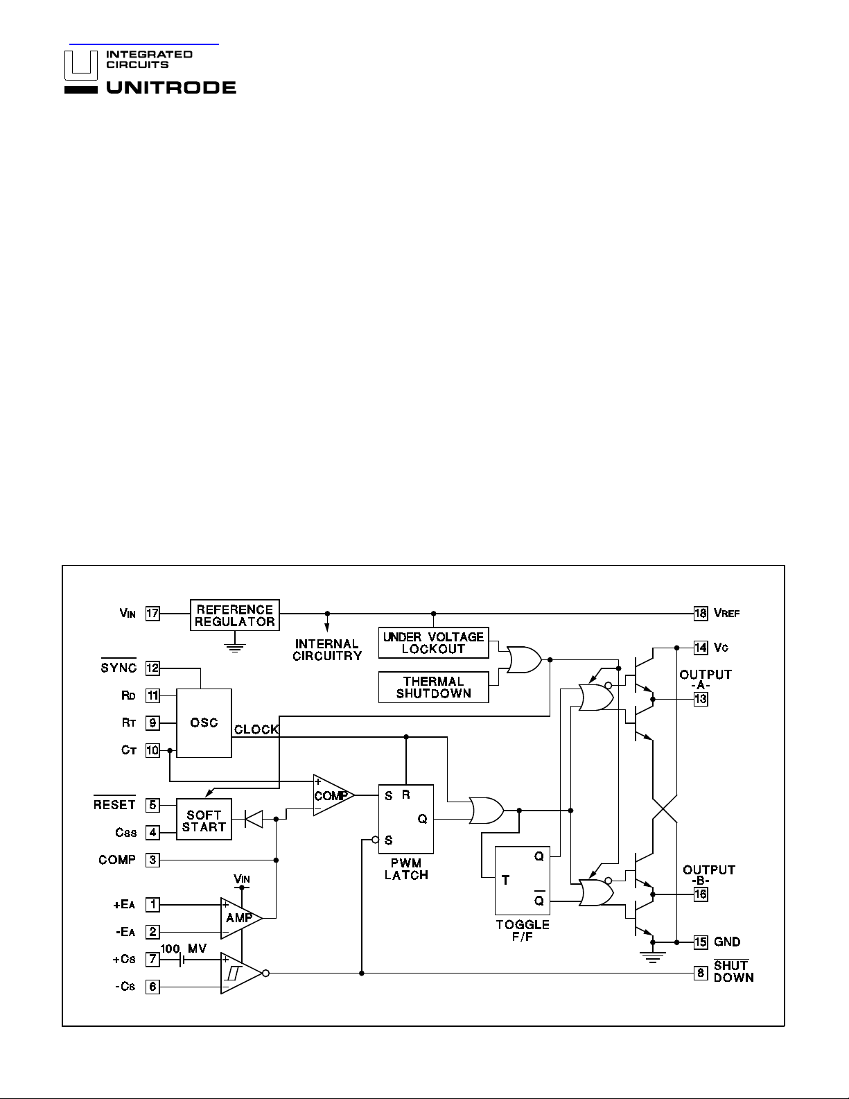
BLOCK DIAGRA M
DESCRIPTION
The UC1526A Series are improved-performance pulse-width modulator circuits intended for direct replacement of equivalent non- “A”
versions in all a pplications. Higher frequency ope ration has been
enhanced by several significant improvements including: a more accurate oscillator with less minimum dead time, reduced circuit delays (particularly i n current limiting), and an improved output stage
with negligible cross-condu ction current. Additional improvements
include the incorporation of a precisi on, band-g ap reference generator, reduced overall supply current, and the addition of thermal
shutdown protection.
Along with these improvements, the UC1526A Series retains the
protective features of under-voltage lockou t, soft-start, digital current limiting, double pulse suppression logic, and adjustable
deadtime. For ease of interfacing, all digital control ports are TTL
compatible with active low logic.
Five volt (5V) operation is possible for “logic level” applications by
connecting V
factory for additional information.
IN, VC and VREF to a precision 5V input supply. Consult
6/93

UC1526A
UC2526A
UC3526A
ABSOLUTE MAXI MUM RATING S (Note 1, 2)
Input Voltage (+VIN) . . . . . . . . . . . . . . . . . . . . . . . . . . . . . . +40V
Collector Supply Voltage (+V
C) . . . . . . . . . . . . . . . . . . . . . +40V
Logic Inputs . . . . . . . . . . . . . . . . . . . . . . . . . . . . -0.3V t o +5.5 V
Analog Input s . . . . . . . . . . . . . . . . . . . . . . . . . . . . -0.3V to +V
Source/ S ink Load Curr ent (each out pu t) . . . . . . . . . . . . 200mA
Referen ce Loa d Curr ent. . . . . . . . . . . . . . . . . . . . . . . . . . 50mA
Logic Sink Curren t . . . . . . . . . . . . . . . . . . . . . . . . . . . . . . 15mA
Power Dissipation at T
Power Dissipation at T
A = +25°C (Note 2) . . . . . . . . . 1000mW
C = +25°C (Note 2). . . . . . . . . . 3000mW
Operating Junct ion Te mp era ture . . . . . . . . . . . . . . . . . . +150°C
Storage Temperature Range . . . . . . . . . . . . . . -65°C to +150°C
Lead Tempera tu re (solder ing, 10 seconds ). . . . . . . . . . +300°C
Note 1: Values beyond which damage may oc cur.
Note 2: Consult packagin g Section of Dat aboo k for ther mal
limitations and considerations of package.
CONNECTION DIAGRAMS
DIL-18, SOIC-18 (TOP VIEW)
J or N Package, DW Package
PLCC-20, LCC- 20
(TOP VIEW)
Q and L Packages
RECOMMENDED OPERATING CONDITIONS
(Note 3)
Input Voltage. . . . . . . . . . . . . . . . . . . . . . . . . . . . . . +7V to +35V
Collector Supply Voltage . . . . . . . . . . . . . . . . . . +4.5V to +35V
Sink/Source Load Cur ren t (each output) . . . . . . . . 0 to 100m A
IN
Reference Load Cur re nt. . . . . . . . . . . . . . . . . . . . . . 0 to 20mA
Oscillator Frequency Range. . . . . . . . . . . . . . . . 1Hz to 600kHz
Oscillator Timing Resistor. . . . . . . . . . . . . . . . . . . 2k Ω to 150kΩ
Oscillator Timing Capacito r. . . . . . . . . . . . . . . . . 400pF to 20µF
Available Deadtime Range at 40kHz . . . . . . . . . . . . 1% to 50%
Operating Am bient Temperature Range
UC1526A. . . . . . . . . . . . . . . . . . . . . . . . . . . . -55°C to +125°C
UC2526A. . . . . . . . . . . . . . . . . . . . . . . . . . . . . -25°C to +85°C
UC3526A. . . . . . . . . . . . . . . . . . . . . . . . . . . . . . . 0°C to +70 ° C
Note 3: Range over which the device is functional and
parame te r limit s are guar ant eed .
PACKAGE PIN FUNCTION
FUNCTION PIN
N/C 1
+ERROR 2
-ERROR 3
COMP. 4
SS 5
C
RESET 6
- CURRENT SENSE 7
+ CURRENT SENSE 8
SHUTDOWN 9
TIMING 10
R
T 11
C
D 12
R
SYNC 13
OUTPUT A 14
C 15
V
N/C 16
GROUND 17
OUTPUT B 18
IN 19
+V
REF 20
V
2

UC1526A
UC2526A
UC3526A
+V
ELECTRICAL CHARACTERISTICS:
PARAMETER TEST CONDITIONS
Reference Sec tion (Note 4)
Output Volt age T
Line Regulatio n +V
Load Regulation I
Temperature Stability Over Operating T
Total Output Voltage
Range
Short Circuit Current V
Under-Voltage Lockout
RESET Output Voltage VREF = 3.8V 0.2 0.4 0.2 0.4 V
Oscillato r Sect io n (Note 6)
Initial Accuracy T
Voltage Stability +V
Temperature Stability Over Operating T
Minimum Frequency R
Maximum Frequency R
Sawtooth Peak Voltage + V
Sawtooth Valley Voltage +V
SYNC Pulse Width TJ = 25°C, RL = 2.7kΩ to V
Error Ampl i fier Section (Note 7)
Input Offs et Vo lta ge R
Input Bias Cur rent -350 -1000 -350 -2000 nA
Input Offs et Cu rr ent 35 100 35 200 nA
DC Open Loop Gai n R
HIGH Output Voltage V
LOW Output Voltage V
Common Mode Rejec tion R
Supply Voltage Rejection +V
PWM Comparator (Note 6)
Minimum Duty Cycle V
Maximum Duty Cycle V
Digi tal Ports (
SYNC, SHUTDOWN, and RESET)
HIGH Output Voltage I
LOW Output Voltage I
HIGH Input Current V
LOW Input Current V
Shutdown Delay From Pin 8, T
Current Limit Compar ato r (Note 8)
Sense Voltage R
Input Bias Cur rent -3 -10 -3 -10 µA
Shutdown Delay From pin 7, 100m V Over driv e, T
Note 4: I
L =
0mA.
Note 5: Guaranteed by design, not 100% tested in product ion.
Note 6: F
OSC
= 40kHz, (RT = 4.12 kΩ ± 1%, CT = 0.01µF± 1%,
D
= 0 Ω).
R
J = +25°C 4.95 5.00 5.05 4.90 5.00 5.10 V
IN = 7 to 35V 2 10 2 15 mV
L = 0 to 20mA 5 20 5 20 mV
Over Recomme nded Opera ting
Conditio ns
REF = 0V 25 50 100 25 50 100 mA
VREF = 4.7V 2.4 4.7 2.4 4.8 V
J = +25°C ±3 ±8 ±3 ±8%
IN = 7 to 35V 0.5 1 0.5 1 %
T = 150kΩ, CT = 20µF (Note 5) 1 1 Hz
T = 2kΩ, CT = 470pF 5 50 650 kHz
IN = 35V 3.0 3.5 3.0 3.5 V
IN =7V 0.5 1.0 0.5 1.0 V
S ≤ 2kΩ 25 210mV
L ≥ 10MΩ 64 72 60 72 dB
PIN 1 - VPIN 2 ≥ 150mV, ISOURCE = 100µA 3.6 4.2 3.6 4.2 V
PIN 2 - VPIN 1 ≥ 150 mV, ISINK = 100µA 0.2 0.4 0.2 0.4 V
S ≤ 2kΩ 70 94 70 94 dB
IN = 12 to 18V 66 80 66 80 dB
COMPENSATION = +0.4V 0 0 %
COMPENSATION = +3.6V 45 49 45 49 %
SOURCE = 40µA 2.4 4.0 2.4 4.0 V
SINK = 3.6mA 0.2 0.4 0 .2 0.4 V
IH = +2.4V -125 -200 -125 -200 µA
IL = +0.4V -225 -36 0 -225 -360 µA
S ≤ 50Ω 90 100 110 80 100 120 mV
IN = 15V, and over operating ambient temper ature, unless ot herwise specified TA = TJ.
UC1526A / UC2526A UC3526A
MIN TYP MAX MIN TYP MAX
J (Note 5) 15 50 15 50 mV
4.90 5.00 5.10 4.85 5.00 5.15 V
J (Note 5) 26 13%
REF
J = 25°C 160 160 ns
J = 25°C 260 260 ns
Note 7: V
Note 8: V
Note 9: V
Note 10 :V
CM
CM
C
IN
1.1 1.1 µs
= 0 to +5.2V
= 0 to +12V.
= +15V .
= +35V , RT = 4.12kΩ.
UNITS
3
 Loading...