


UC1526
UC2526
UC3526
DESCRIPTION
The UC1526 is a high performance monolithic pulse width modulator
circuit designed for fixed-frequency switching regulators and other
power control appl ications. Included in an 18-pin dual-in-line package are a temperature compensated voltage reference, sawtooth oscillator, error amplifier, pulse width modulator, pulse metering and
setting logic, and two low impedance power drivers. Also included
are protective features such as soft-start and under-voltage lockout,
digital current limiting, double pulse inhibit, a data latch for single
pulse metering, adjustable deadtime, and provision for symmetry correction inputs. For ease of interface, all digital control ports are TTL
and B-series CMOS compatible. Active LOW logic design allows
wired-OR connections for maximum flexibilit y. This versatile device
can be used to impl ement single-ende d or push-p ull switching regulators of either polarity, both transformerless and transformer coupled. The UC1526 is characterized for operation over the full military
temperature range of -55°C to +125°C. The UC2526 is characterized
for operation from -25°C to +85°C, and the UC3526 is characterized
for operation from 0° to +70°C.
查询UC1526供应商
Regulating Pulse Width Modulat or
FEATURES
• 8 To 35V Operation
• 5V Reference Trimmed To ±1%
• 1Hz To 400kHz Oscillator Range
• Dual 100mA Source/Sink Outputs
• Digital Current Limiting
• Double Pulse Suppression
• Programmable Deadtime
• Under-Voltage Lockout
• Single Pulse Metering
• Programmable Soft-Start
• Wide Current Limit Common Mode Range
• TTL/CMOS Compatible Logic Ports
• Symmetry Correction Capability
• Guaranteed 6 Unit Synchronization
BLOCK DIAGRA M
6/93
ABSOLUTE MAXI MUM RATING S (Note 1, 2)
UC1526
UC2526
UC3526
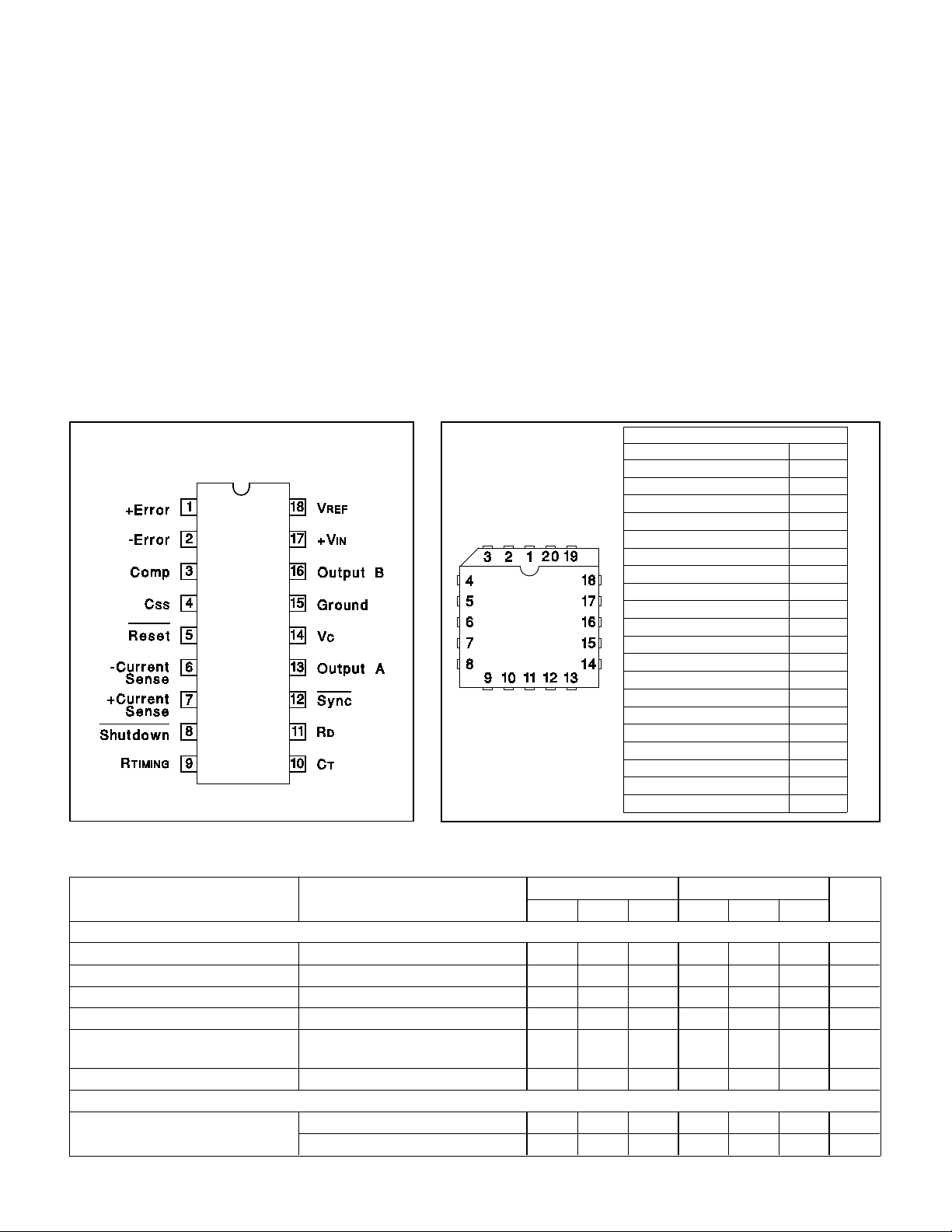
PACKAGE PIN FUNCTION
FUNCTION PIN
N/C 1
+Error 2
-Error 3
Comp. 4
CSS 5
Reset
______
6
- Current Sense 7
+ Current Sense 8
Shutdown
_________
9
RTIMING 10
CT 11
RD 12
Sync 13
Output A 14
VC 15
N/C 16
Ground 17
Output B 18
+VIN 19
VREF 20
+VIN = 15V, and over operating ambient temperature, unles s ot herwise
specified, TA = TJ.
Input Voltage (+VIN) . . . . . . . . . . . . . . . . . . . . . . . . . . . . . . +40V
Collector Supply Voltage (+V
C) . . . . . . . . . . . . . . . . . . . . . +40V
Logic Inputs . . . . . . . . . . . . . . . . . . . . . . . . . . . . . -0.3V to +5.5V
Analog Input s . . . . . . . . . . . . . . . . . . . . . . . . . . . . . - 0.3V to +V
Source/S ink Load Current (ea ch out pu t) . . . . . . . . . . . . . 200mA
Referen ce Loa d Curr ent. . . . . . . . . . . . . . . . . . . . . . . . . . . 50mA
Logic Sink Curren t . . . . . . . . . . . . . . . . . . . . . . . . . . . . . . . 15mA
Power Dissipation at T
Power Dissipation at T
A = +25°C (Note 2). . . . . . . . . . 1000mW
C = +25°C (Note 2). . . . . . . . . . 3000mW
Operating Junct ion Te mp era tu re . . . . . . . . . . . . . . . . . . +150°C
Storage Tem per ature Range . . . . . . . . . . . . . . -65°C to +150°C
Lead Temp era tu re (solder ing, 10 seconds ). . . . . . . . . . +300°C
Note 1: Values beyo nd which da mage may occ ur.
Note 2: Consult packaging section of databo ok for ther m al
limitations and co nsider ations of pac kage .
CONNECTION DIAGRAMS
RECOMMENDED OPERATING CONDITIONS (Note 3)
Input Voltage . . . . . . . . . . . . . . . . . . . . . . . . . . . . . . +8V to +35V
Collector Supply Voltage . . . . . . . . . . . . . . . . . . . +4.5V to +35V
Sink/Source Lo ad Cur ren t (each out put ). . . . . . . . . 0 to 100mA
Reference Load Cur re nt . . . . . . . . . . . . . . . . . . . . . . 0 to 20mA
IN
Oscillator Frequency Range . . . . . . . . . . . . . . . . 1Hz to 400kHz
Oscillator Timing Resistor . . . . . . . . . . . . . . . . . . . 2kΩ to 150kΩ
Oscillator Timing Capacito r . . . . . . . . . . . . . . . . . . . 1nF to 20µF
Available Deadtime Range at 40kHz. . . . . . . . . . . . . 3% to 50%
Operating Am bient Temperature Range
UC1526 . . . . . . . . . . . . . . . . . . . . . . . . . . . . -55°C to +125°C
UC2526 . . . . . . . . . . . . . . . . . . . . . . . . . . . . . -25°C to +85°C
UC3526 . . . . . . . . . . . . . . . . . . . . . . . . . . . . . . -0°C to +70°C
Note 3: Range over which the device is funct ional and
parameter lim its are guarant eed.
DIL-18, SOIC- 18 (T O P VIEW)
J or N Package, DW Package
PLCC-20, LCC-20
(TOP VIEW )
Q and L Packages
ELECTRICAL CHARACTERISTICS:
Reference Sec tio n (Note 4)
Output Volt age T
Line Regulatio n +V
Load Regulation I
Temperature Stability Over Operating T
Total Output
Voltage Range
Short Circuit Current V
Under -Voltage Lockout
_______
RESET
Note 4: IL = 0mA.
PARAMETER TEST CONDITIONS UC1526 / UC2526 UC3526 UNITS
J = + 25°C 4.95 5.00 5.05 4.90 5.00 5.10 V
IN = 8 to 35V 10 20 10 30 mV
L = 0 to 20mA 10 30 10 50 mV
J 15 50 15 50 mV
Over Recommended
Operating Con dition s
REF = 0V 25 50 100 25 50 100 mA
Output Volt age V
REF = 3.8V 0.2 0.4 0.2 0.4 V
V
REF = 4.8V 2.4 4.8 2.4 4.8 V
MIN TYP MAX MIN TYP MAX
4.90 5.00 5.10 4.85 5.00 5.15 V
2
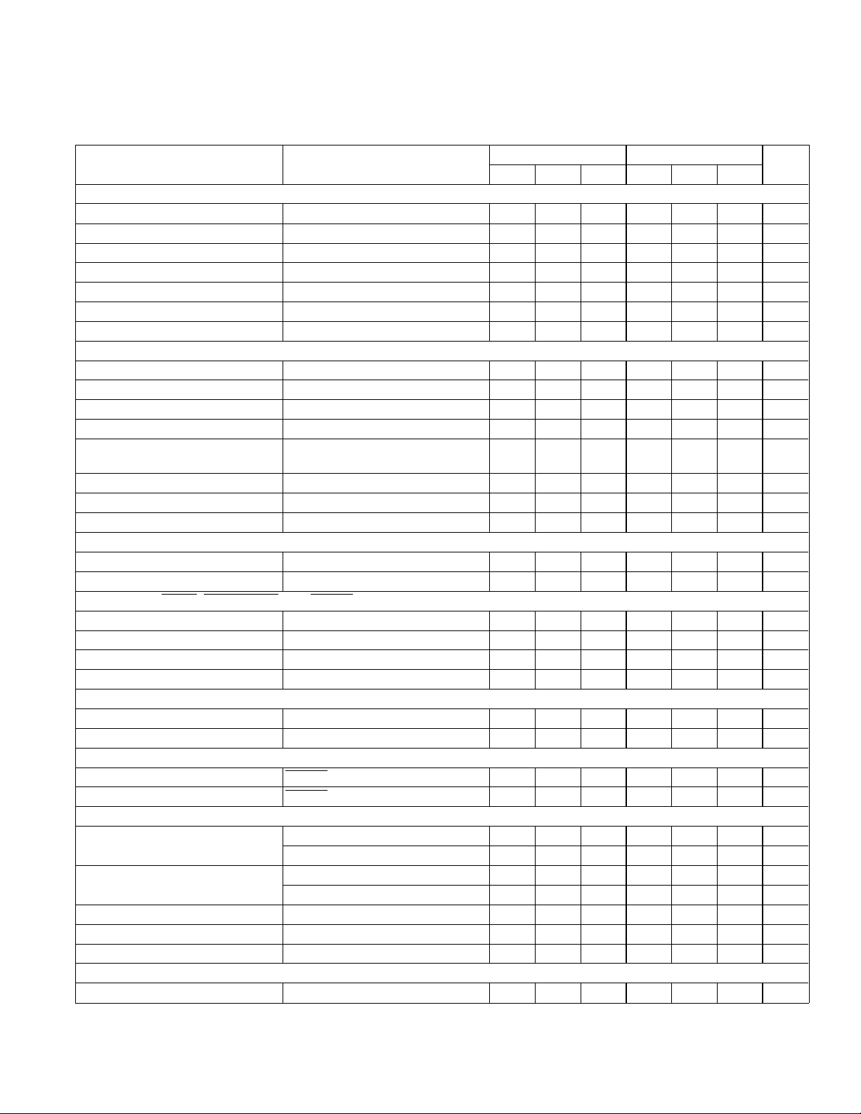
ELECTRICAL CHARACTERIST ICS :
+VIN = 15V, and over operating ambient temper at ure, unless othe rwise
specified, TA = TJ.
UC1526
UC2526
UC3526
PARAMETER TEST CONDI TIO NS UC1526 / UC2526 UC3526 UNITS
MIN TYP MAX MIN TYP MAX
Oscillator Section (Note 5)
Initial Accuracy T
Voltage Sta bi lity +V
Temperature Stability Over Operating T
Minimum Frequency R
Maximum Fr equency R
Sawtooth Peak Volt age +V
Sawtooth Valley Voltage +V
Err or Am p lifier Section ( Note 6)
Input Offset Voltage R
Input Bias Current -350 -1000 -350 -2000 nA
Input Offset Current 35 100 35 200 nA
DC Open Loop Gain R
HIGH Output Volt age V
LOW Outpu t Voltage V
Common Mode Rejection Rs ≤ 12kΩ 70 94 70 94 dB
Supply Voltage Rejec tion +V
PWM Compar ator (Note 5)
Minimum Duty Cycle V
Maximum Duty Cycle V
Digital Ports (
SYNC, SHUTDOWN, and RESET)
HIGH Output Volt age I
LOW Outpu t Voltage I
HIGH Input Curren t V
LOW Input Current V
Current LImit Comparator ( Not e 7)
Sense Voltage R
Input Bias Current -3 -10 -3 -10 µA
Soft-Start Sect ion
Error Clamp Voltage
Cs Charging Current
Output Dri ve rs (Each Out put ) ( Note 8)
HIGH Output Volt age I
LOW Outpu t Voltage I
Collector Leakage V
Rise Time CL = 1000pF 0.3 0.6 0.3 0.6 µs
Fall Time CL = 1000pF 0.1 0.2 0.1 0.2 µ s
Power Consumption (Note 9)
Standby Curre nt SHUTDOW N
J = + 25°C ±3 ±8 ±3 ±8%
IN = 8 to 35V 0.5 1 0.5 1 %
J 710 3 5%
T = 150kΩΩ, CT = 20µµF11Hz
T = 2kΩΩ, CT = 1.0nF 400 400 kHz
IN = 35V 3.0 3.5 3.0 3.5 V
IN = 8V 0.5 1.0 0.5 1.0 V
S ≤≤ 2kΩΩ 25 210mV
L ≥ 10MΩΩ 64 72 60 72 dB
PIN1-VPIN2 ≥≥ 150m V, ISOURCE =
3.6 4.2 3.6 4.2 V
100µµA
PIN2-VPIN1 ≥≥ 150mV, ISINK = 100µµA 0.2 0.4 0.2 0.4 V
IN = 12 to 18V 66 80 66 80 dB
COMPENSATION = +0.4V 0 0 %
COMPENSATION = +3.6V 45 49 45 49 %
SOURCE =40µµA 2.4 4.0 2.4 4.0 V
SINK = 3.6mA 0.2 0.4 0.2 0.4 V
IH = +2.4V -125 -200 -125 -200 µA
IL = +0.4V -225 -360 -225 -360 µA
S ≤≤ 50ΩΩ 90 100 110 80 100 120 mV
RESET = +0.4V 0.1 0.4 0.1 0.4 V
RESET =+2.4V 50 100 150 50 100 150 µA
SOURCE = 20mA 12.5 13.5 12.5 13.5 V
I
SOURCE = 100mA 12 1 3 12 13 V
SINK = 20mA 0.2 0.3 0.2 0.3 V
I
SINK = 100mA 1.2 2.0 1.2 2.0 V
C = 40V 50 150 50 150 µA
____________
=
+0.4V 18 30 18 30 mA
Note 4: IL = 0mA.
OSC
Note 5: F
R
= 40kHz (RT = 4.12k
D
= 0Ω)
Ω ±
1%, CT = 0.1µF ± 1%,
Note 6: V
Note 8: V
Note 9: +V
3
CM
= 0 to +5.2 V
C
= +15V
IN
= +35V, RT = 4.12k
Ω
 Loading...