

Page 1

Copernicus™ GPS Receiver
Reference Manual
Part Number 58052-00
Revision A
July 2006
Page 2

Corporate Office
Hardware Limited Warranty
Trimble Navigation Limited
935 Stewart Drive
Sunnyvale, CA 94085
U.S.A.
Phone: +1-408-481-8000, 1-800-827-8000
www.trimble.com
Support
+1-800-767-4822 (USA and Canada)
+1-913-338-8225 (International)
Copyright and Trademarks
© 2006 Trimble Navigation Limited. All rights reserved. No
part of this manual may be copied, reproduced, translated, or
reduced to any electronic medium or machine-readable form
for any use other than with the Copernicus™ GPS Receiver.
The Globe & Triangle logo, Trimble, Colossus, FirstGPS, and
Lassen, are trademarks of Trimble Navigation Limited.
The Sextant logo with Trimble is a trademark of Trimble
Navigation Limited, registered in the United States Patent and
Trademark Off ice .
All other trademarks are the property of their respective
owners.
Release Notice
This is the May 2006 release (Revision A) of the Copernicus™
GPS Receiver System Designer Reference Manual, part
number 58052-00.
Trimble warrants that this Trimble hardware product (the
“Product”) shall be free from defects in materials and
workmanship and will substantially conform to Trimble’s
applicable published specifications for the Product for a period
of one (1) year, starting from the date of delivery. The warranty
set forth in this paragraph shall not apply to software/firmware
products.
Software and Firmware License, Limited Warranty
This Trimble software and/or firmware product (the
“Software”) is licensed and not sold. Its use is governed by the
provisions of the applicable End User License Agreement
(“EULA”), if any, included with the Software. In the absence
of a separate EULA included with the Software providing
different limited warranty terms, exclusions, and limitations,
the following terms and conditions shall apply. Trimble
warrants that this Trimble Software product will substantially
conform to Trimble’s applicable published specifications for
the Software for a period of ninety (90) days, starting from the
date of delivery.
Warranty Remedies
Trimble's sole liability and your exclusive remedy under the
warranties set forth above shall be, at Trimble’s option, to
repair or replace any Product or Software that fails to conform
to such warranty (“Nonconforming Product”), or refund the
purchase price paid by you for any such Nonconforming
Product, upon your return of any Nonconforming Product to
Trimble in accordance with Trimble’s standard return material
authorization procedures.
Warranty Exclusions and Disclaimer
The following limited warranties give you specific legal rights.
You may have others, which vary from state/jurisdiction to
state/jurisdiction.
Waste Electrical and Electronic Equipment (WEEE)
Notice
This Trimble product is furnished on an OEM basis. By
incorporating this Trimble product with your finished goods
product(s) you shall be deemed the “producer” of all such
products under any laws, regulations or other statutory scheme
providing for the marking, collection, recycling and/or
disposal of electrical and electronic equipment (collectively,
“WEEE Regulations”) in any jurisdiction whatsoever, (such as
for example national laws implementing EC Directive 2002/96
on waste electrical and electronic equipment, as amended), and
shall be solely responsible for complying with all such
applicable WEEE Regulations.
Restriction on Hazardous Substances
As of July 1, 2006, the Product is compliant in all material
respects with DIRECTIVE 2002/95/EC OF THE EUROPEAN
P ARLIAMENT AND OF THE C OUNCIL of 27 January 2003
on the restriction of the use of certain hazardous substances in
electrical and electronic equipment (RoHS Directive) and
Amendment 2005/618/EC filed under C(2005) 3143, with
exemptions for lead in solder pursuant to Paragraph 7 of the
Annex to the RoHS Directive applied. The foregoing is limited
to Product placed on the market in the Member States of the
European Union on or after 1 July 2006. Trimble has relied on
representations made by its suppliers in certifying this Product
as RoHS compliant.
These warranties shall be applied only in the event and to the
extent that: (i) the Products and Software are properly and
correctly installed, configured, interfaced, maintained, stored,
and operated in accordance with Trimble’s relevant operator's
manual and specifications, and; (ii) the Products and Software
are not modified or misused.
The preceding warranties shall not apply to, and Trimble shall
not be responsible for defects or performance problems
resulting from (i) the combination or utilization of the Product
or Software with products, information, data, systems or
devices not made, supplied or specified by Trimble; (ii) the
operation of the Product or Software under any specification
other than, or in addition to, Trimble's standard specifications
for its products; (iii) the unauthorized modification or use of
the Product or Software; (iv) damage caused by accident,
lightning or other electrical discharge, fresh or salt water
immersion or spray; or (v) normal wear and tear on
consumable parts (e.g., batteries).
Page 3

THE WARRANTIES ABOVE STATE TRIMBLE'S ENTIRE
LIABILITY, AND YOUR EXCLUSIVE REMEDIES, RELATING
TO PERFORMANCE OF THE PRODUCTS AND SOFTWARE.
EXCEPT AS OTHERWISE EXPRESSLY PROVIDED HEREIN,
THE PRODUCTS, SOFTWARE, AND ACCOMPANYING
DOCUMENTATION AND MATERIALS ARE PROVIDED “AS-
IS” AND WITHOUT EXPRESS OR IMPLIED WARRANTY OF
ANY KIND BY EITHER TRIMBLE NAVIGATION LIMITED OR
ANYONE WHO HAS BEEN INVOLVED IN ITS CREATION,
PRODUCTION, INSTALLATION, OR DISTRIBUTION,
INCLUDING, BUT NOT LIMITED TO, THE IMPLIED
WARRANTIES OF MERCHANTABILITY AND FITNESS FOR A
PARTICULAR PURPOSE, TITLE, AND NONINFRINGEMENT.
THE STATED EXPRESS WARRANTIES ARE IN LIEU OF ALL
OBLIGATIONS OR LIABILITIES ON THE PART OF TRIMBLE
ARISING OUT OF, OR IN CONNECTION WITH, ANY
PRODUCTS OR SOFTWARE. SOME STATES AND
JURISDICTIONS DO NOT ALLOW LIMITATIONS ON
DURATION OR THE EXCLUSION OF AN IMPLIED
WARRANTY, SO THE ABOVE LIMITATION MAY NOT APPLY
TO YOU.
TRIMBLE NAVIGATION LIMITED IS NOT RESPONSIBLE FOR
THE OPERATION OR FAILURE OF OPERATION OF GPS
SATELLITES OR THE AVAILABILITY OF GPS SATELLITE
SIGNALS.
Limitation of Liability
TRIMBLE’S ENTIRE LIABILITY UNDER ANY PROVISION
HEREIN SHALL BE LIMITED TO THE GREATER OF THE
AMOUNT PAID BY YOU FOR THE PRODUCT OR SOFTWARE
LICENSE OR U.S.$25.00. TO THE MAXIMUM EXTENT
PERMITTED BY APPLICABLE LAW, IN NO EVENT SHALL
TRIMBLE OR ITS SUPPLIERS BE LIABLE FOR ANY
INDIRECT, SPECIAL, INCIDENTAL, OR CONSEQUENTIAL
DAMAGES WHATSOEVER UNDER ANY CIRCUMSTANCE OR
LEGAL THEORY RELATING IN ANY WAY TO THE
PRODUCTS, SOFTWARE, AND ACCOMPANYING
DOCUMENTATION AND MATERIALS, (INCLUDING,
WITHOUT LIMITATION, DAMAGES FOR LOSS OF BUSINESS
PROFITS, BUSINESS INTERRUPTION, LOSS OF BUSINESS
INFORMATION, OR ANY OTHER PECUNIARY LOSS),
REGARDLESS OF WHETHER TRIMBLE HAS BEEN ADVISED
OF THE POSSIBILITY OF ANY SUCH LOSS AND
REGARDLESS OF THE COURSE OF DEALING WHICH
DEVELOPS OR HAS DEVELOPED BETWEEN YOU AND
TRIMBLE. BECAUSE SOME STATES AND JURISDICTIONS
DO NOT ALLOW THE EXCLUSION OR LIMITATION OF
LIABILITY FOR CONSEQUENTIAL OR INCIDENTAL
DAMAGES, THE ABOVE LIMITATION MAY NOT APPLY TO
YOU.
Page 4

Page 5

Table of Contents
Table of Contents
1 GENERAL DESCRIPTION
Receiver Overview . . . . . . . . . . . . . . . . . . . . . . . . . . . . . . . . . . . . . . . . . . 6
Starter Kit . . . . . . . . . . . . . . . . . . . . . . . . . . . . . . . . . . . . . . . . . . . . . . . 6
Key Features . . . . . . . . . . . . . . . . . . . . . . . . . . . . . . . . . . . . . . . . . . . . . 7
Block Diagram . . . . . . . . . . . . . . . . . . . . . . . . . . . . . . . . . . . . . . . . . 7
Performance Specifications . . . . . . . . . . . . . . . . . . . . . . . . . . . . . . . . . . . . . . 8
Interface Characteristics . . . . . . . . . . . . . . . . . . . . . . . . . . . . . . . . . . . . . . . 8
Electrical Characteristics . . . . . . . . . . . . . . . . . . . . . . . . . . . . . . . . . . . . . . . 9
Physical Characteristics. . . . . . . . . . . . . . . . . . . . . . . . . . . . . . . . . . . . . . . . 9
Environmental Specifications. . . . . . . . . . . . . . . . . . . . . . . . . . . . . . . . . . . . . 9
Ordering Information . . . . . . . . . . . . . . . . . . . . . . . . . . . . . . . . . . . . . . . . 10
2 INTERFACE CHARACTERISTICS
Pin Assignments . . . . . . . . . . . . . . . . . . . . . . . . . . . . . . . . . . . . . . . . . . 12
Pin Description . . . . . . . . . . . . . . . . . . . . . . . . . . . . . . . . . . . . . . . . . . . 13
Detailed Pin Descriptions . . . . . . . . . . . . . . . . . . . . . . . . . . . . . . . . . . 14
Protocols . . . . . . . . . . . . . . . . . . . . . . . . . . . . . . . . . . . . . . . . . . . . . . 16
Serial Ports Default Settings . . . . . . . . . . . . . . . . . . . . . . . . . . . . . . . . . . . . 17
Pulse-Per-Second (PPS) in Copernicus Receiver. . . . . . . . . . . . . . . . . . . . . . . . . . 18
3 ELECTRICAL SPECIFICATIONS
Absolute Minimum and Maximum Limits . . . . . . . . . . . . . . . . . . . . . . . . . . . . . 20
Normal Operating Conditions. . . . . . . . . . . . . . . . . . . . . . . . . . . . . . . . . . . . 20
Power Consumption over Temperature and Voltage . . . . . . . . . . . . . . . . . . . . . . . . 22
ESD Protection . . . . . . . . . . . . . . . . . . . . . . . . . . . . . . . . . . . . . . . . . . . 22
4 OPERATING MODES
Copernicus Receiver Operating Modes. . . . . . . . . . . . . . . . . . . . . . . . . . . . . . . 24
Run Mode . . . . . . . . . . . . . . . . . . . . . . . . . . . . . . . . . . . . . . . . . . . . . . 24
Standby Mode. . . . . . . . . . . . . . . . . . . . . . . . . . . . . . . . . . . . . . . . . . . . 24
Monitor Mode. . . . . . . . . . . . . . . . . . . . . . . . . . . . . . . . . . . . . . . . . . . . 24
Changing the RUN/STANDBY modes . . . . . . . . . . . . . . . . . . . . . . . . . . . . . . . 25
Using the XSTANDBY Pin to Switch Modes . . . . . . . . . . . . . . . . . . . . . . . . 25
Using Serial Ports to Switch Modes . . . . . . . . . . . . . . . . . . . . . . . . . . . . . 25
Saving the Almanac into the Flash Memory . . . . . . . . . . . . . . . . . . . . . . . . . . . . 27
Graceful Shutdown. . . . . . . . . . . . . . . . . . . . . . . . . . . . . . . . . . . . . . 27
Almanac in Flash Updating Process . . . . . . . . . . . . . . . . . . . . . . . . . . . . . 27
18-Hour RTC Roll Over . . . . . . . . . . . . . . . . . . . . . . . . . . . . . . . . . . . . . . 28
Copernicus GPS Receiver v
Page 6

Table of Contents
5 COPERNICUS GPS APPLICATION CIRCUITS
Passive antenna—Minimum Connections . . . . . . . . . . . . . . . . . . . . . . . . . . . . . 30
Active Antenna—Full Connection . . . . . . . . . . . . . . . . . . . . . . . . . . . . . . . . . 32
Active Antenna—No Antenna Status. . . . . . . . . . . . . . . . . . . . . . . . . . . . . . . . 34
6 RF LAYOUT CONSIDERATIONS
General Recommendations . . . . . . . . . . . . . . . . . . . . . . . . . . . . . . . . . . . . . 36
Design considerations for RF Track Topologies . . . . . . . . . . . . . . . . . . . . . . . . . . 37
PCB Considerations . . . . . . . . . . . . . . . . . . . . . . . . . . . . . . . . . . . . . . . . 38
MIcrostrip Transmission Lines. . . . . . . . . . . . . . . . . . . . . . . . . . . . . . . . 38
Stripline Transmission Lines. . . . . . . . . . . . . . . . . . . . . . . . . . . . . . . . . 39
7 MECHANICAL SPECIFICATIONS
Mechanical Outline Drawing . . . . . . . . . . . . . . . . . . . . . . . . . . . . . . . . . . . . 42
Guidelines for soldering the Copernicus module to a PCB. . . . . . . . . . . . . . . . . . . . . 43
Solder mask . . . . . . . . . . . . . . . . . . . . . . . . . . . . . . . . . . . . . . . . . 43
Pad Pattern . . . . . . . . . . . . . . . . . . . . . . . . . . . . . . . . . . . . . . . . . . 44
Paste Mask . . . . . . . . . . . . . . . . . . . . . . . . . . . . . . . . . . . . . . . . . . 45
8 PACKAGING
Introduction . . . . . . . . . . . . . . . . . . . . . . . . . . . . . . . . . . . . . . . . . . . . . 48
Reel . . . . . . . . . . . . . . . . . . . . . . . . . . . . . . . . . . . . . . . . . . . . . . . . . 49
Tapes . . . . . . . . . . . . . . . . . . . . . . . . . . . . . . . . . . . . . . . . . . . . . . . . 50
9 SHIPPING AND HANDLING
Handling . . . . . . . . . . . . . . . . . . . . . . . . . . . . . . . . . . . . . . . . . . . . . . 52
Shipment . . . . . . . . . . . . . . . . . . . . . . . . . . . . . . . . . . . . . . . . . . . . . . 52
Storage . . . . . . . . . . . . . . . . . . . . . . . . . . . . . . . . . . . . . . . . . . . . . . . 52
Moisture Indicator . . . . . . . . . . . . . . . . . . . . . . . . . . . . . . . . . . . . . . . . . 52
Floor Life . . . . . . . . . . . . . . . . . . . . . . . . . . . . . . . . . . . . . . . . . . . . . . 52
Moisture Precondition . . . . . . . . . . . . . . . . . . . . . . . . . . . . . . . . . . . . . . . 53
Recommended Baking Procedure. . . . . . . . . . . . . . . . . . . . . . . . . . . . . . . . . . 53
Soldering Paste . . . . . . . . . . . . . . . . . . . . . . . . . . . . . . . . . . . . . . . . . . . 54
Solder Reflow. . . . . . . . . . . . . . . . . . . . . . . . . . . . . . . . . . . . . . . . . . . . 54
Recommended Soldering Profile . . . . . . . . . . . . . . . . . . . . . . . . . . . . . . . . . . 55
Optical Inspection. . . . . . . . . . . . . . . . . . . . . . . . . . . . . . . . . . . . . . . . . . 55
Cleaning. . . . . . . . . . . . . . . . . . . . . . . . . . . . . . . . . . . . . . . . . . . . . . . 56
Repeated Reflow Soldering. . . . . . . . . . . . . . . . . . . . . . . . . . . . . . . . . . . . . 56
Wave Soldering . . . . . . . . . . . . . . . . . . . . . . . . . . . . . . . . . . . . . . . . . . . 56
Hand Soldering . . . . . . . . . . . . . . . . . . . . . . . . . . . . . . . . . . . . . . . . . . . 56
Rework . . . . . . . . . . . . . . . . . . . . . . . . . . . . . . . . . . . . . . . . . . . . . . . 56
Conformal Coating . . . . . . . . . . . . . . . . . . . . . . . . . . . . . . . . . . . . . . . . . 56
Grounding the Metal Shield. . . . . . . . . . . . . . . . . . . . . . . . . . . . . . . . . . . . . 57
vi Copernicus GPS Receiver
Page 7

Table of Contents
10 COPERNICUS REFERENCE BOARD
Introduction . . . . . . . . . . . . . . . . . . . . . . . . . . . . . . . . . . . . . . . . . . . . . 60
Copernicus Reference Board Block Diagram. . . . . . . . . . . . . . . . . . . . . . . . . . . . 62
Copernicus Reference Board Schematic . . . . . . . . . . . . . . . . . . . . . . . . . . . . . . 63
Copernicus Reference Board I/O and power Connector . . . . . . . . . . . . . . . . . . . . . . 65
Copernicus Reference Board Power Requirement . . . . . . . . . . . . . . . . . . . . . . . . . 65
Copernicus Reference Board Jumper Table. . . . . . . . . . . . . . . . . . . . . . . . . . . . . 66
Reference Board Component Locations Drawing . . . . . . . . . . . . . . . . . . . . . . . . . 67
11 COPERNICUS STARTER KIT
Introduction . . . . . . . . . . . . . . . . . . . . . . . . . . . . . . . . . . . . . . . . . . . . . 70
Interface Unit. . . . . . . . . . . . . . . . . . . . . . . . . . . . . . . . . . . . . . . . . 70
Serial Port Interface. . . . . . . . . . . . . . . . . . . . . . . . . . . . . . . . . . . . . . . . . 72
Loading the FTDI Driver. . . . . . . . . . . . . . . . . . . . . . . . . . . . . . . . . . . 72
Default Settings . . . . . . . . . . . . . . . . . . . . . . . . . . . . . . . . . . . . . . . 72
Starter Kit Interface Connections . . . . . . . . . . . . . . . . . . . . . . . . . . . . . . . . . . 73
Removing the Reference Board from the Interface Unit . . . . . . . . . . . . . . . . . . . . . . 75
Antenna . . . . . . . . . . . . . . . . . . . . . . . . . . . . . . . . . . . . . . . . . . . . . . . 76
Using a Passive Antenna. . . . . . . . . . . . . . . . . . . . . . . . . . . . . . . . . . . 76
Pulse-Per-Second (PPS) . . . . . . . . . . . . . . . . . . . . . . . . . . . . . . . . . . . . . . 77
Quick Start Guide . . . . . . . . . . . . . . . . . . . . . . . . . . . . . . . . . . . . . . . . . . 78
12 FIRMWARE UPGRADE
Introduction . . . . . . . . . . . . . . . . . . . . . . . . . . . . . . . . . . . . . . . . . . . . . 82
Software Architecture. . . . . . . . . . . . . . . . . . . . . . . . . . . . . . . . . . . . . . . . 82
Boot Monitor . . . . . . . . . . . . . . . . . . . . . . . . . . . . . . . . . . . . . . . . . . . . 83
Firmware Binary File Format. . . . . . . . . . . . . . . . . . . . . . . . . . . . . . . . . . . . 83
Firmware Loading Procedure . . . . . . . . . . . . . . . . . . . . . . . . . . . . . . . . . . . . 84
Pseudo-code . . . . . . . . . . . . . . . . . . . . . . . . . . . . . . . . . . . . . . . . . 84
Pseudo-Code Explanation . . . . . . . . . . . . . . . . . . . . . . . . . . . . . . . . . . 86
Error Recovery . . . . . . . . . . . . . . . . . . . . . . . . . . . . . . . . . . . . . . . . 88
Monitor Interface Protocol . . . . . . . . . . . . . . . . . . . . . . . . . . . . . . . . . . . . . 89
Protocol Format . . . . . . . . . . . . . . . . . . . . . . . . . . . . . . . . . . . . . . . 89
Data Transmission . . . . . . . . . . . . . . . . . . . . . . . . . . . . . . . . . . . . . . 89
Monitor Mode Packet Descriptions . . . . . . . . . . . . . . . . . . . . . . . . . . . . . 90
ENQ, ACK, NAK . . . . . . . . . . . . . . . . . . . . . . . . . . . . . . . . . . . . . . 90
Packet ID – 0x96 (Boot ROM Version Report) . . . . . . . . . . . . . . . . . . . . . . . 90
Packet ID – 0x8F (Erase Firmware Section). . . . . . . . . . . . . . . . . . . . . . . . . 91
FlashLoader Tool Reference Guide. . . . . . . . . . . . . . . . . . . . . . . . . . . . . . . . . 94
Introduction . . . . . . . . . . . . . . . . . . . . . . . . . . . . . . . . . . . . . . . . . 94
File and Folder Structure. . . . . . . . . . . . . . . . . . . . . . . . . . . . . . . . . . . 94
Source Code Reference . . . . . . . . . . . . . . . . . . . . . . . . . . . . . . . . . . . 94
Compiling and Generating the Executable. . . . . . . . . . . . . . . . . . . . . . . . . . 95
Copernicus GPS Receiver vii
Page 8

Table of Contents
A TRIMBLE STANDARD INTERFACE PROTOCOL (TSIP)
Interface Scope . . . . . . . . . . . . . . . . . . . . . . . . . . . . . . . . . . . . . . . . . . . 98
Run Mode Packet Structure. . . . . . . . . . . . . . . . . . . . . . . . . . . . . . . . . . . . . 99
Automatic Output Packets . . . . . . . . . . . . . . . . . . . . . . . . . . . . . . . . . . . . .100
Customizing Receiver Operations . . . . . . . . . . . . . . . . . . . . . . . . . . . . . . . . .100
Automatic Position and Velocity Reports. . . . . . . . . . . . . . . . . . . . . . . . . . . . . .101
Initialization Packets to Speed Start-up. . . . . . . . . . . . . . . . . . . . . . . . . . . . . . .102
Packets Output at Power-Up . . . . . . . . . . . . . . . . . . . . . . . . . . . . . . . . . . . .102
Timing Packets . . . . . . . . . . . . . . . . . . . . . . . . . . . . . . . . . . . . . . . . . . .103
Satellite Data Packets . . . . . . . . . . . . . . . . . . . . . . . . . . . . . . . . . . . . . . . .103
Backwards Compatibility . . . . . . . . . . . . . . . . . . . . . . . . . . . . . . . . . . . . . .103
Guidelines for Use with Copernicus GPS . . . . . . . . . . . . . . . . . . . . . . . . . . . . .104
Recommended TSIP Packets . . . . . . . . . . . . . . . . . . . . . . . . . . . . . . . . . . . . 1 06
Command Packets Sent to the Receiver . . . . . . . . . . . . . . . . . . . . . . . . . . . . . . 107
Report Packets Sent by the Receiver to the User . . . . . . . . . . . . . . . . . . . . . . . . . .108
Key Setup Parameters or Packet BB . . . . . . . . . . . . . . . . . . . . . . . . . . . . . . . .109
Dynamics Code . . . . . . . . . . . . . . . . . . . . . . . . . . . . . . . . . . . . . . .109
Elevation Mask. . . . . . . . . . . . . . . . . . . . . . . . . . . . . . . . . . . . . . . .110
Signal Level Mask . . . . . . . . . . . . . . . . . . . . . . . . . . . . . . . . . . . . . .110
Packet Descriptions . . . . . . . . . . . . . . . . . . . . . . . . . . . . . . . . . . . . . . . . .111
Packet Descriptions Used in Run Mode . . . . . . . . . . . . . . . . . . . . . . . . . . .111
Command Packet 0x1E - Clear Battery Backup, then Reset. . . . . . . . . . . . . . . . .113
Command Packet 0x1F - Request Software Versions . . . . . . . . . . . . . . . . . . . .113
Command Packet 0x21 - Request Current Time. . . . . . . . . . . . . . . . . . . . . . .113
Command Packet 0x23 - Initial Position (XYZ ECEF) . . . . . . . . . . . . . . . . . . .113
Command Packet 0x24 - Request GPS Receiver Position Fix Mode . . . . . . . . . . . .114
Command Packet 0x25 - Initiate Soft Reset & Self Test . . . . . . . . . . . . . . . . . .114
Command Packet 0x26 - Request Health . . . . . . . . . . . . . . . . . . . . . . . . . .114
Command Packet 0x27 - Request Signal Levels. . . . . . . . . . . . . . . . . . . . . . .114
Command Packet 0x2B - Initial Position (Latitude, Longitude, Altitude). . . . . . . . . .114
Command Packet 0x2D - Request Oscillator Offset. . . . . . . . . . . . . . . . . . . . .115
Command Packet 0x2E - Set GPS Time. . . . . . . . . . . . . . . . . . . . . . . . . . .115
Command Packet 0x31 - Accurate Initial Position (XYZ ECEF). . . . . . . . . . . . . .115
Command Packet 0x32 - Accurate Initial Position, (Latitude, Longitude, Altitude) . . . .116
Command Packet 0x35 - Set Request I/O Options . . . . . . . . . . . . . . . . . . . . .117
Command Packet 0x37 - Request Status and Values of Last Position and Velocity. . . . .119
Command Packet 0x38 - Request/Load Satellite System Data . . . . . . . . . . . . . . .119
Command Packet 0x3A - Request Last Raw Measurement . . . . . . . . . . . . . . . . .120
Command Packet 0x3C - Request Current Satellite Tracking Status . . . . . . . . . . . .120
Report Packet 0x41 - GPS Time . . . . . . . . . . . . . . . . . . . . . . . . . . . . . . .120
Report Packet 0x42 - Single-Precision Position Fix, XYZ ECEF . . . . . . . . . . . . . .121
Report Packet 0x43 - Velocity Fix, XYZ ECEF . . . . . . . . . . . . . . . . . . . . . . .122
viii Copernicus GPS Receiver
Page 9

Table of Contents
Report Packet 0x45 - Software Version Information . . . . . . . . . . . . . . . . . . . .122
Report Packet 0x46 - Health of Receiver . . . . . . . . . . . . . . . . . . . . . . . . . .123
Report Packet 0x47 - Signal Levels for all Satellites . . . . . . . . . . . . . . . . . . . .123
Report Packet 0x4A - Single Precision LLA Position Fix. . . . . . . . . . . . . . . . . .124
Report Packet 0x4B - Machine/Code ID and Additional Status. . . . . . . . . . . . . . .125
Report Packet 0x4D - Oscillator Offset . . . . . . . . . . . . . . . . . . . . . . . . . . .125
Report Packet 0x4E - Response to Set GPS Time . . . . . . . . . . . . . . . . . . . . . .126
Report Packet 0x55 - I/O Options . . . . . . . . . . . . . . . . . . . . . . . . . . . . . .126
Report Packet 0x56 - Velocity Fix, East-North-Up (ENU) . . . . . . . . . . . . . . . . .127
Report Packet 0x57 - Information About Last Computed Fix. . . . . . . . . . . . . . . .128
Report Packet 0x58 - Satellite System Data/Acknowledge from Receiver . . . . . . . . .128
Report Packet 0x5A - Raw Measurement Data . . . . . . . . . . . . . . . . . . . . . . .131
Report Packet 0x5C - Satellite Tracking Status . . . . . . . . . . . . . . . . . . . . . . .133
Report Packet 0x6D - All-In-View Satellite Selection. . . . . . . . . . . . . . . . . . . .134
Command Packet 0x7A . . . . . . . . . . . . . . . . . . . . . . . . . . . . . . . . . . .134
Report Packet 0x7B . . . . . . . . . . . . . . . . . . . . . . . . . . . . . . . . . . . . .135
Command Packet 0x7E - TAIP Message Output . . . . . . . . . . . . . . . . . . . . . .136
Report Packet 0x83 - Double-Precision XYZ Position Fix and Bias Information. . . . . .138
Report Packet 0x84 - Double-Precision LLA Position Fix and Bias Information. . . . . .139
Packets 0x8E and 0x8F - Superpacket . . . . . . . . . . . . . . . . . . . . . . . . . . . .139
Command Packet 0xBB - Navigation Configuration . . . . . . . . . . . . . . . . . . . .140
Command Packet 0xBC - Protocol Configuration. . . . . . . . . . . . . . . . . . . . . .141
Command Packet 0xC0 - Graceful Shutdown and Go To Standby Mode . . . . . . . . . .143
TSIP Superpackets . . . . . . . . . . . . . . . . . . . . . . . . . . . . . . . . . . . . . . . . .145
Command Packet 8E-4A - Set/Request Copernicus GPS Cable Delay
and PPS Polarity. . . . . . . . . . . . . . . . . . . . . . . . . . . . . . . . . . . .145
Command Packet 8E-4A - Set/Request Copernicus GPS Cable Delay
and PPS Polarity. . . . . . . . . . . . . . . . . . . . . . . . . . . . . . . . . . . .146
Command Packet 8E-15 - Set/Request Datum. . . . . . . . . . . . . . . . . . . . . . . .146
Command Packet 0x8E-17 - Request Last Position or Auto-Report Position in UTM Single
Precision Format . . . . . . . . . . . . . . . . . . . . . . . . . . . . . . . . . . .147
Command Packet 8E-18 - Request Last Position or Auto Report Position in UTM Double
Precision Format . . . . . . . . . . . . . . . . . . . . . . . . . . . . . . . . . . .147
Report Packet 0x8F-15 - Current Datum Values. . . . . . . . . . . . . . . . . . . . . . .148
Report Packet 8F-17 - UTM Single Precision Output . . . . . . . . . . . . . . . . . . . .149
Report Packet 8F-18 - UTM Double Precision Output . . . . . . . . . . . . . . . . . . .150
Command Packet 0x8E-20 - Request Last Fix with Extra Information . . . . . . . . . . .151
Report Packet 0x8F-20 - Last Fix with Extra Information (binary fixed point) . . . . . . .151
Command Packet 0x8E-26 - Non-Volatile Memory Storage . . . . . . . . . . . . . . . .153
Report Packet 0x8F-26 - Non-Volatile Memory Status . . . . . . . . . . . . . . . . . . .154
Datums . . . . . . . . . . . . . . . . . . . . . . . . . . . . . . . . . . . . . . . . . . . . . . .155
Copernicus GPS Receiver ix
Page 10

Table of Contents
B COPERNICUS MONITOR USER’S GUIDE
Copernicus Monitor. . . . . . . . . . . . . . . . . . . . . . . . . . . . . . . . . . . . . . . . .164
TSIP Reader . . . . . . . . . . . . . . . . . . . . . . . . . . . . . . . . . . . . . . . . .164
TSIP Demo. . . . . . . . . . . . . . . . . . . . . . . . . . . . . . . . . . . . . . . . . .164
Copernicus Monitor. . . . . . . . . . . . . . . . . . . . . . . . . . . . . . . . . . . . . . . . .165
Data Logging . . . . . . . . . . . . . . . . . . . . . . . . . . . . . . . . . . . . . . . . . . . .166
TSIP and NMEA Support. . . . . . . . . . . . . . . . . . . . . . . . . . . . . . . . . . . . . .166
C NMEA 0183
The NMEA 0183 Communication Interface . . . . . . . . . . . . . . . . . . . . . . . . . . . .168
NMEA 0183 Message Format . . . . . . . . . . . . . . . . . . . . . . . . . . . . . . . . . . .169
Field Definitions . . . . . . . . . . . . . . . . . . . . . . . . . . . . . . . . . . . . . . . . . .170
Checksum . . . . . . . . . . . . . . . . . . . . . . . . . . . . . . . . . . . . . . . . . . . . . .171
Exception Behavior . . . . . . . . . . . . . . . . . . . . . . . . . . . . . . . . . . . . . . . . .172
Power-up with No Back-up Data on SRAM. . . . . . . . . . . . . . . . . . . . . . . . .172
Power-up with Back-up Data on SRAM. . . . . . . . . . . . . . . . . . . . . . . . . . .172
Interruption of GPS Signal. . . . . . . . . . . . . . . . . . . . . . . . . . . . . . . . . .172
NMEA 0183 Message Options . . . . . . . . . . . . . . . . . . . . . . . . . . . . . . . . . . .173
NMEA 0183 Message Formats . . . . . . . . . . . . . . . . . . . . . . . . . . . . . . . . . . .175
GGA - GPS Fix Data. . . . . . . . . . . . . . . . . . . . . . . . . . . . . . . . . . . . . 175
GLL - Geographic Position - Latitude/Longitude . . . . . . . . . . . . . . . . . . . . . .176
GSA - GPS DOP and Active Satellites . . . . . . . . . . . . . . . . . . . . . . . . . . .176
GSV - GPS Satellites in View . . . . . . . . . . . . . . . . . . . . . . . . . . . . . . . .177
RMC - Recommended Minimum Specific GPS/Transit Data . . . . . . . . . . . . . . . .177
VTG - Track Made Good and Ground Speed . . . . . . . . . . . . . . . . . . . . . . . .178
ZDA - Time & Date . . . . . . . . . . . . . . . . . . . . . . . . . . . . . . . . . . . . .179
AH - Almanac Health . . . . . . . . . . . . . . . . . . . . . . . . . . . . . . . . . . . .180
AL - Almanac Page . . . . . . . . . . . . . . . . . . . . . . . . . . . . . . . . . . . . .182
AS - Almanac Status . . . . . . . . . . . . . . . . . . . . . . . . . . . . . . . . . . . . .183
BA - Antenna Status . . . . . . . . . . . . . . . . . . . . . . . . . . . . . . . . . . . . .184
CR - Configure Receiver. . . . . . . . . . . . . . . . . . . . . . . . . . . . . . . . . . .185
DM - Datum . . . . . . . . . . . . . . . . . . . . . . . . . . . . . . . . . . . . . . . . .186
EM - Enter Monitor Mode . . . . . . . . . . . . . . . . . . . . . . . . . . . . . . . . . . 186
EP - Ephemeris. . . . . . . . . . . . . . . . . . . . . . . . . . . . . . . . . . . . . . . .187
IO Ionosphere . . . . . . . . . . . . . . . . . . . . . . . . . . . . . . . . . . . . . . . .189
KG - Set Initial Position . . . . . . . . . . . . . . . . . . . . . . . . . . . . . . . . . . .189
NM - Automatic Message Output . . . . . . . . . . . . . . . . . . . . . . . . . . . . . .190
PS - PPS Configuration . . . . . . . . . . . . . . . . . . . . . . . . . . . . . . . . . . .191
PT - Serial Port Configuration . . . . . . . . . . . . . . . . . . . . . . . . . . . . . . . .192
RT - Reset . . . . . . . . . . . . . . . . . . . . . . . . . . . . . . . . . . . . . . . . . .193
TF - Receiver Status and Position Fix . . . . . . . . . . . . . . . . . . . . . . . . . . . .194
UT - UTC . . . . . . . . . . . . . . . . . . . . . . . . . . . . . . . . . . . . . . . . . .195
VR - Version . . . . . . . . . . . . . . . . . . . . . . . . . . . . . . . . . . . . . . . . .195
x Copernicus GPS Receiver
Page 11

Table of Contents
D TRIMBLE ASCII INTERFACE PROT OCOL (TAIP)
Message Format. . . . . . . . . . . . . . . . . . . . . . . . . . . . . . . . . . . . . . . . . . .199
Start of a New Message . . . . . . . . . . . . . . . . . . . . . . . . . . . . . . . . . . .199
Message Qualifier . . . . . . . . . . . . . . . . . . . . . . . . . . . . . . . . . . . . . .200
Message Identifier . . . . . . . . . . . . . . . . . . . . . . . . . . . . . . . . . . . . . .200
Data String . . . . . . . . . . . . . . . . . . . . . . . . . . . . . . . . . . . . . . . . . . 200
Vehicle ID . . . . . . . . . . . . . . . . . . . . . . . . . . . . . . . . . . . . . . . . . .200
Checksum . . . . . . . . . . . . . . . . . . . . . . . . . . . . . . . . . . . . . . . . . .201
Message Delimiter . . . . . . . . . . . . . . . . . . . . . . . . . . . . . . . . . . . . . .201
Sample PV Message . . . . . . . . . . . . . . . . . . . . . . . . . . . . . . . . . . . . . . . .202
Time and Distance Reporting. . . . . . . . . . . . . . . . . . . . . . . . . . . . . . . . . . . .203
Latitude and Longitude Conversion . . . . . . . . . . . . . . . . . . . . . . . . . . . . . . . .205
Message Data Strings . . . . . . . . . . . . . . . . . . . . . . . . . . . . . . . . . . . . . . . .206
AL Altitude/Up Velocity . . . . . . . . . . . . . . . . . . . . . . . . . . . . . . . . . . . .207
CP Compact Position Solution. . . . . . . . . . . . . . . . . . . . . . . . . . . . . . . . .208
ID Identification Number . . . . . . . . . . . . . . . . . . . . . . . . . . . . . . . . . . .209
IP Initial Position . . . . . . . . . . . . . . . . . . . . . . . . . . . . . . . . . . . . . . .210
LN Long Navigation Message . . . . . . . . . . . . . . . . . . . . . . . . . . . . . . . . .211
PR Protocol. . . . . . . . . . . . . . . . . . . . . . . . . . . . . . . . . . . . . . . . . . . 212
PT Port Characteristic . . . . . . . . . . . . . . . . . . . . . . . . . . . . . . . . . . . . .213
PV Position/Velocity Solution . . . . . . . . . . . . . . . . . . . . . . . . . . . . . . . . .214
RM Reporting Mode . . . . . . . . . . . . . . . . . . . . . . . . . . . . . . . . . . . . . .215
RT Reset Mode. . . . . . . . . . . . . . . . . . . . . . . . . . . . . . . . . . . . . . . . .216
ST Status . . . . . . . . . . . . . . . . . . . . . . . . . . . . . . . . . . . . . . . . . . . .217
TM Time/Date . . . . . . . . . . . . . . . . . . . . . . . . . . . . . . . . . . . . . . . . .219
VR Version Number . . . . . . . . . . . . . . . . . . . . . . . . . . . . . . . . . . . . . .220
X1 Extended Status. . . . . . . . . . . . . . . . . . . . . . . . . . . . . . . . . . . . . . .221
Communication Scheme for TAIP221
Query for Single Sentence . . . . . . . . . . . . . . . . . . . . . . . . . . . . . . . . . .221
Scheduled Reporting Frequency Interval . . . . . . . . . . . . . . . . . . . . . . . . . .221
The Response to Query or Scheduled Report . . . . . . . . . . . . . . . . . . . . . . . .222
The Set Qualifier . . . . . . . . . . . . . . . . . . . . . . . . . . . . . . . . . . . . . . .222
Sample Communication Session. . . . . . . . . . . . . . . . . . . . . . . . . . . . . . . 222
E TAIP MONITOR USER’S GUIDE
TAIP Monitor . . . . . . . . . . . . . . . . . . . . . . . . . . . . . . . . . . . . . . . . . . . .226
Data Logging . . . . . . . . . . . . . . . . . . . . . . . . . . . . . . . . . . . . . . . . . . . .227
Copernicus GPS Receiver xi
Page 12

Table of Contents
xii Copernicus GPS Receiver
Page 13

List of Figures
List of Figures
Figure 1.1 Copernicus Block Diagram. . . . . . . . . . . . . . . . . . . . . . . . . . . . . . . . . 7
Figure 2.1 Copernicus Pin Assignments . . . . . . . . . . . . . . . . . . . . . . . . . . . . . . . 12
Figure 4.1 Current Draw Levels in Standby Mode. . . . . . . . . . . . . . . . . . . . . . . . . . 28
Figure 4.2 Issuing three (3) NULL characters for exiting Standby Mode . . . . . . . . . . . . . . 28
Figure 5.1 Application Drawing: Passive Antenna - Minimum Connections . . . . . . . . . . . . 30
Figure 5.2 Passive antenna - HW Activated Standby Mode Available . . . . . . . . . . . . . . . 31
Figure 5.3 Application Drawing: Active antenna - Full connection . . . . . . . . . . . . . . . . . 32
Figure 5.4 Application Drawing: Active antenna - No Antenna Status . . . . . . . . . . . . . . . 34
Figure 6.1 Microstrip Transmission Lines . . . . . . . . . . . . . . . . . . . . . . . . . . . . . . 38
Figure 6.2 PCB Microstrip Topology . . . . . . . . . . . . . . . . . . . . . . . . . . . . . . . . 38
Figure 6.3 Stripline Transmission Lines . . . . . . . . . . . . . . . . . . . . . . . . . . . . . . . 39
Figure 7.1 Copernicus GPS Receiver, Footprint. . . . . . . . . . . . . . . . . . . . . . . . . . . 42
Figure 7.2 Copernicus GPS Receiver, Outline Dimensions . . . . . . . . . . . . . . . . . . . . . 42
Figure 7.3 Solder Mask Diagram. . . . . . . . . . . . . . . . . . . . . . . . . . . . . . . . . . . 43
Figure 7.4 Pad Pattern Diagram . . . . . . . . . . . . . . . . . . . . . . . . . . . . . . . . . . . 44
Figure 7.5 Paste Mask Diagram . . . . . . . . . . . . . . . . . . . . . . . . . . . . . . . . . . . 45
Figure 8.1 Copernicus GPS Receiver Packaged in Tape. . . . . . . . . . . . . . . . . . . . . . . 48
Figure 8.2 Reel Diagram . . . . . . . . . . . . . . . . . . . . . . . . . . . . . . . . . . . . . . . 49
Figure 8.3 Tape Diagram. . . . . . . . . . . . . . . . . . . . . . . . . . . . . . . . . . . . . . . 50
Figure 8.4 Feeding Direction Diagram. . . . . . . . . . . . . . . . . . . . . . . . . . . . . . . . 50
Figure 9.1 Moisture Precondition Label . . . . . . . . . . . . . . . . . . . . . . . . . . . . . . . 53
Figure 9.2 Recommended Soldering Profile . . . . . . . . . . . . . . . . . . . . . . . . . . . . . 55
Figure 10.1 Copernicus Reference Board, Frontside . . . . . . . . . . . . . . . . . . . . . . . . . 60
Figure 10.2 Copernicus Reference Board, Backside . . . . . . . . . . . . . . . . . . . . . . . . . 61
Figure 10.3 Copernicus Reference Board Block Diagram . . . . . . . . . . . . . . . . . . . . . . 62
Figure 10.4 Copernicus Reference Board Schematic (Page 1) . . . . . . . . . . . . . . . . . . . . 63
Figure 10.5 Copernicus Reference Board Schematic (Page 2) . . . . . . . . . . . . . . . . . . . . 64
Figure 10.6 Copernicus Reference Board Schematic (Page 3) . . . . . . . . . . . . . . . . . . . . 64
Figure 10.7 Copernicus Reference Board, Top Side . . . . . . . . . . . . . . . . . . . . . . . . . 67
Figure 10.8 Copernicus Reference Board Schematic, Bottom Side. . . . . . . . . . . . . . . . . . 67
Figure 11.1 Interface Unit . . . . . . . . . . . . . . . . . . . . . . . . . . . . . . . . . . . . . . . 70
Figure 11.2 AC/DC Power Supply Converter . . . . . . . . . . . . . . . . . . . . . . . . . . . . . 71
Figure 11.3 USB Cable . . . . . . . . . . . . . . . . . . . . . . . . . . . . . . . . . . . . . . . . 71
Figure 11.4 Front side of the Interface Unit . . . . . . . . . . . . . . . . . . . . . . . . . . . . . . 73
Figure 11.5 Connecting Power . . . . . . . . . . . . . . . . . . . . . . . . . . . . . . . . . . . . 78
Figure 11.6 Conxall Connection. . . . . . . . . . . . . . . . . . . . . . . . . . . . . . . . . . . . 78
Figure 11.7 Connecting the Antenna . . . . . . . . . . . . . . . . . . . . . . . . . . . . . . . . . 79
Copernicus GPS Receiver xiii
Page 14

List of Figures
Figure B.1 Copernicus Monitor Serial Port Selection . . . . . . . . . . . . . . . . . . . . . . . .165
Figure B.2 Copernicus Monitor - Main Window. . . . . . . . . . . . . . . . . . . . . . . . . . .165
Figure E.1 TAIP Monitor - Serial Port Selection. . . . . . . . . . . . . . . . . . . . . . . . . . .226
Figure E.2 TAIP Monitor - Main Window . . . . . . . . . . . . . . . . . . . . . . . . . . . . . .227
xiv Copernicus GPS Receiver
Page 15

CHAPTER
1
GENERAL DESCRIPTION 1
In this chapter:
• Receiver Overview
•Starter Kit
• Key Features
• Block Diagram
• Performance Specifications
• Interface Characteristics
• Electrical Characteristics
• Physical Characteristics
• Environmental Specifications
• Ordering Information
Page 16

1 GENERAL DESCRIPTION
1.1 Receiver Overview
Trimble's Copernicus™ GPS receiver delivers proven performance and Trimble quality
for a new generation of position-enabled products. It features the Trimble revolutionary
TrimCore™ software technology for extremely fast startup times and high performance in
foliage canopy, multipath and urban canyon environments.
Designed for the demands of automated, pick and place, high-volume production
processes, the Copernicus module is a complete 12-channel GPS receiver in a 19mm x
19mm x 2.54mm, thumbnail-sized shielded unit. The small, thin, single-sided module is
packaged in tape and reel for pick and place manufacturing processes; 28 reflowsolderable edge castellations provide interface to your design without costly I/O and RF
connectors. Each module is manufactured and factory tested to Trimble's highest quality
standards.
The ultra-sensitive Copernicus GPS receiver can acquire GPS satellite signals and
generate fast position fixes with high accuracy in extremely challenging environments and
under poor signal conditions. The module consumes less than 94 mW typically at full
power with continuous tracking. The Copernicus GPS receiver has been designed to meet
restrictions on the use of hazardous substances under the RoHS European Directive.
The Copernicus GPS module is a complete drop-in, ready-to-go receiver that provides
position, velocity and time data in a choice of three protocols. Trimble's powerful TSIP
protocol offers complete control over receiver operation and provides detailed satellite
information. The TAIP protocol is an easy-to-use ASCII protocol designed specifically for
track and trace applications. The bi-directional NMEA 0183 v3.0 protocol offers industrystandard data messages and a command set for easy interface to mapping software.
Compatible with active or passive antenna designs, the Copernicus GPS receiver is perfect
for portable handheld, battery-powered applications. The receiver's small size and low
power requirement make it ideal for use in Bluetooth appliances, sport accessories,
personal navigators, cameras, computer and communication peripherals, as well as,
vehicle and asset tracking, navigation, and security applications.
1.2 Starter Kit
The Copernicus Starter Kit provides everything you need to get started integrating stateof-the-art GPS capability into your application. The kit includes the reference interface
board, which gives designers a visual layout of the Copernicus module on a PCB including
the RF signal trace and RF connector, as well as the I/O connections of the 28 signal pins.
Also included are a power converter, power adapter, GPS antennas, and the software for
the user to readily evaluate the ease of adding Copernicus GPS to an application.
6 Copernicus GPS Receiver
Page 17
1.3 Key Features
• Thumbnail-sized: 19 mm W x 19 mm L (0.75" W x 0.75" L)
• Ultra-thin design: 2.54 mm H (0.1")
• Fast manufacturing: Pick & place assembly, Tape & reel packaging, Reflow
solderable
• No I/O or RF connector; 28 Edge castellations
• Ultra-low power usage: less than 94 mW (typical)
• Highly sensitive:
−152 dBm Tracking Sensitivity
−142 dBm Acquisition Sensitivity
• Fast TTFF (cold start): 39 sec
• Supports active or passive antenna designs
• 12-channel simultaneous operation
• Supports NMEA 0183, TSIP and TAIP protoc ols
GENERAL DESCRIPTION 1
• Reference board and starter kit available
• RoHS compliant (Lead-free)
• High quality, low price
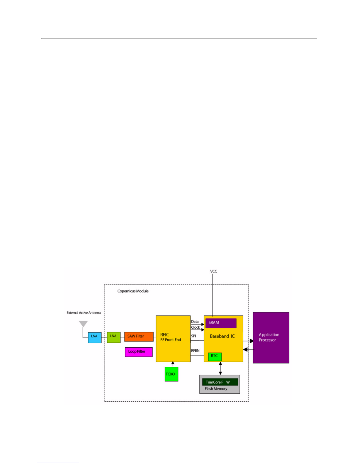
1.3.1 Block Diagram
Figure 1.1 Copernicus Block Diagram
Copernicus GPS Receiver 7
Page 18

1 GENERAL DESCRIPTION
1.4 Performance Specifications
Performance Specifications
L1 (1575.42 MHz) frequency, C/A code, 12-channel, continuous
tracking receiver
Update Rate
TSIP 1 Hz
NMEA 1 Hz
TAIP 1 Hz
Accuracy
Horizontal <3 meters (50%), <8 meters
Altitude <10 meters (50%), <16 meters
Velocity 0.06 m/sec
PPS (static) ±50 nanoseconds
Acquisition (Autonomous Operation)
Reacquisition 2 sec
Hot Start 9 sec
Warm Start 35 sec
Cold Start 39 sec
Out of the Box 41 sec
Sensitivity
Tracking -152 dBm
Acquisition -142 dBm
Operational
Speed Limit 515 m/s
(90%)
(90%)
1.5 Interface Characteristics
Interface Characteristics
Connectors 28 surface mount edge castellations
Serial Port 2 serial ports (transmit/receive)
PPS 3.0 V CMOS-compatible TTL-level pulse,
Protocols Supports TSIP*, TAIP** and NMEA*** 0183
The following abbreviations are used to refer to the interface protocols:
• Trimble Standard Interface Protocol, TSIP
• Trimble ASCII Interface Protocol, TAIP
• National Marine Electronics Association, NMEA
8 Copernicus GPS Receiver
once per second
v3.0 Bi-directional NMEA Messages
Page 19

1.6 Electrical Characteristics
Electrical Specifications
Prime Power +2.7 VDC to 3.3 VDC
Power Consumption (typ.) 30.7 mA (82.9 mW) @ 2.7 V
Backup Power +2.7 VDC to +3.3 VDC
Ripple Noise Max 50 mV, peak-to-peak from 1 Hz to 1 MHz
1.7 Physical Characteristics
Physical Specifications
Enclosure Metal shield
Dimensions 19 mm W x 19 mm L x 2.54 mm H (0.75" W x
Weight 1.7 grams (0.06 ounce) including shield
GENERAL DESCRIPTION 1
(typ.) 31.3 mA (93.9 mW) @ 3.0 V
0.75" L x 0.1" H)
1.8 Environmental S pecifications
Electrical Specifications
Operating Temperature -40° C to +85° C
Storage Temperature -55° C to +105° C
Vibration 0.008 g2/Hz 5 Hz to 20 Hz
Operating Humidity 5% to 95% R.H. non-condensing, at +60° C
0.05 g2/Hz 20 Hz to 100 Hz
-3 dB/octave 100 Hz to 900 Hz
Copernicus GPS Receiver 9
Page 20

1 GENERAL DESCRIPTION
1.9 Ordering Information
Ordering Information
Copernicus GPS Receiver Module Single module in metal enclos u re
Reference Board P/N 58054-00
Starter Kit Non-RoHS: PN 58050-00
P/N 58048-00
Copernicus GPS module mounted on a carrier
board with I/O and RF connectors for evaluation
purposes, including the RF circuitry with the
antenna open detection, as well as antenna short
detection and protection.
RoHS (Lead-free version): P/N 58050-05
Includes Copernicus Reference Board
mounted on interface motherboard in a
durable metal enclosure, AC/DC power
converter, compact magnetic-mount GPS
antenna, serial interface cable, cigarette
lighter adapter, TSIP, NMEA, and TAIP
protocols, software toolkit and manual on
CD-ROM.
10 Copernicus GPS Receiver
Page 21

CHAPTER
2
INTERFACE CHARACTERISTICS 2
In this chapter:
• Pin Assignments
• Pin Description
• Protocols
• Serial Ports Default Settings
• Pulse-Per-Second (PPS) in Copernicus Receiver
Page 22
2 INTERFACE CHARACTERISTICS
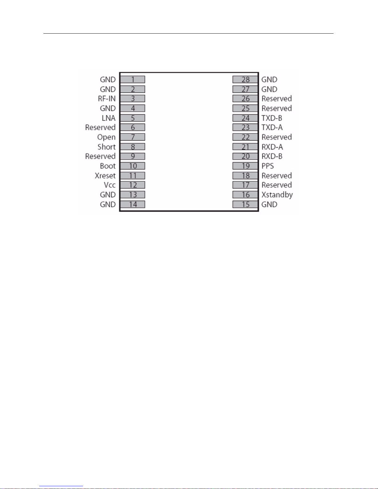
2.1 Pin Assignments
Figure 2.1 Copernicus Pin Assignments
12 Copernicus GPS Receiver
Page 23

INTERFACE CHARACTERISTICS 2
2.2 Pin Description
T able 2.1 Pin Description
Pin Name Description Function Note
1 GND Ground G Signal ground. Connect to common ground.
2 GND RF Ground G One of two RF grounds adjacent to RF input.
Connect to RF ground system.
3 RF Input GPS RF input I 50-ohm unbalanced (coaxial) RF input.
4 GND RF Ground G One of two RF grounds adjacent to RF input.
Connect to RF ground system.
5 LNA_XEN LNA Enable O Can be used with active antennas only. Active
low logic level signal to control external LNA.
6 Reserved Reserved I/O Do not connect.
7 OPEN Antenna OPEN I Logic level from external antenna detection
circuit. See “Antenna Detect Truth Table”.
8 SHORT Antenna SHORT I Logic level from external antenna detection
circuit. See “Antenna Detect Truth Table”.
9 Reserved Reserved I Connect to VCC.
10 Reserved Reserved I Connect to VCC.
1 1 XRESET Reset I Active low logic level reset. Connect to VCC with
or without a pullup resistor, if not used.
12 VCC Supply voltage P Module power supply 2.7 - 3.3 VDC
13 GND Ground G Signal ground. Connect to common ground.
14 GND Ground G Signal ground. Connect to common ground.
15 GND Ground G Signal ground. Connect to common ground.
16 XST ANDBY Run/Standby I Selects “RUN” or “STANDBY” mode. Connect to
VCC if not used (run only).
17 Reserved Reserved I/O Do not connect.
18 Reserved Reserved I/O Do not connect.
19 PPS Pulse per second O Logic level timing signal at 1 Hz. Do not connect
if not used.
20 RXD_B Serial port B receive I Logic level secondary serial port receive.
21 RXD_A Serial port A receive I Logic level primary serial port receive.
22 Reserved Reserved I/O Do not connect.
23 TXD_A Serial port A transmit O Logic level primary serial port transmit.
24 TXD_B Serial port B transmit O Logic level secondary serial port transmit.
25 Reserved Reserved I/O Do not connect.
26 Reserved Reserved I/O Do not connect.
27 GND Ground G Signal ground. Connect to common ground.
28 GND Ground G Signal ground. Connect to common ground.
Index: G: Ground; I: Input; O: Output; P: Power
Copernicus GPS Receiver 13
Page 24

2 INTERFACE CHARACTERISTICS
2.2.1 Detailed Pin Descriptions
RF Input
This pin is the 50 ohm unbalanced GPS RF input. It can be used with active or passive
antennas.
Passive antennas: This pin may be connected by a low-loss 50 ohm unbalanced
transmission system to the passive GPS antenna if loss is minimal (< 2 dB).
Active Antennas: It can also be connected to the output of an external low-noise amplifier,
which is amplifying GPS signals from an antenna. The gain of the LNA must be great
enough to overcome transmission losses from the LNA output to this pin. The
specification for noise figure for the module is < 3 dB at room temperature and < 4 dB
over the specified temperature range, -40 to +85 C. The external LNA must be located
such that the loss from the GPS antenna connection to the LNA input is minimized,
preferably < 1 dB. The noise figure of the LNA should be as low as possible, preferably
< 2 dB. The specifications are provided so that a cascaded noise figure design calculation
can be used. Active antennas must be powered with a single bias-Tee circuit. (See
applications circuits in Chapter 5.)
LNA_XEN
This logic level output can be used to control power to an external LNA or other circuitry.
The logic of this signal is such that when the module is running (not in standby), this signal
is low. During “STANDBY” mode, this signal is high. This pin may be used to control the
gate of a p-channel FET used as a switch.
Open/Short Pins
If using an active antenna, Trimble recommends that the user implement an antenna
detection circuit with short circuit protection. There are two pins provided for reporting the
antenna status: OPEN and SHORT.
The following logic level inputs may be used with a detection circuit (with or without
protection) to monitor the status of the external LNA of an active antenna by the module.
The truth table for the logic of these signals is provided below. These input pins conform
to the Input / Output Pin threshold levels specified in Table 3.2.
14 Copernicus GPS Receiver
Page 25

INTERFACE CHARACTERISTICS 2
Table 2.2 Antenna Status Truth Table
Condition of logic signals
ANTENNA REPORTS SHORT OPEN
Antenna Open Reported 1 1
Antenna Normal Reported 1 0
Antenna Shorted Reported 0 0
Undefined 0 1
If using a passive antenna and the SHORT and OPEN pins are floating, the receiver will
report an open condition. If a normal condition from the receiver is desired when using a
passive antenna, set the logic levels of the SHORT pin High and the OPEN pin Low.
XRESET
This logic-level, active low input is used to issue hardware or power-on reset to the
module. It may be connected to external logic or to a processor to issue reset, if desired. To
reset the module, take this pin low for at least 100 microseconds. This pin must be tied to
VCC with a resistance of less than 10 K Ohms if not used.
The hardware reset deletes all the information saved in SRAM (position time, almanac,
ephemeris and customers' user set configurations if not previously saved in non-volatile
Flash memory) and restarts the Copernicus receiver.
VCC
This is the primary voltage supply pin for the module. This pin also provides power during
Standby Mode (Backup Mode). If it is desired to have separate power supplies for main
power and Standby Mode (Backup Mode) power, an external diode-pair must be provided.
XSTANDBY
This logic level input is used to control the RUN/STANDBY state of the module. If this
signal is high, the unit will run normally. If this signal is low, the unit will go to
“STANDBY” mode.
PPS
Pulse-per-second. This logic level output provides a 1 Hz timing signal to external devices.
The positive going 4.2 usec pulse delay is controllable by firmware packet 0x35. This
output meets the Input / Output Pin Threshold Specifications in Table 3.2.
RXD_A and RXD_B
These logic level inputs are the primary (A) and secondary (B) serial port receive lines
(data input to the module). These inputs meet the Input / Output Pin Threshold
Specifications in Table 3.2. The baud rate for the two ports is under firmware control.
Copernicus GPS Receiver 15
Page 26

2 INTERFACE CHARACTERISTICS
TXD_A and TXD_B
These logic level outputs are the primary (A) and secondary (B) serial port transmit lines
(data moving away from the module). These outputs meet the Input / Output Pin Threshold
Specifications in Table 3.2. The baud rate for the two ports is under firmware control.
Reserved Pins
There are 8 reserved pins on the Copernicus GPS Receiver. For the recommended pin
connections for these reserved pins, please refer to Table 2.1.
2.3 Protocols
T able 2.3 Copernicus GPS Receiver Available protocols
Protocols Specification Direction Serial Port Support
NMEA NMEA 0183 v3.0; Bi-directional
with extended NMEA sentences
TSIP (Trimble S tandard
Interface Protocol)
T AIP (Trimble ASCII
Interface Protocol)
Trimble propriety binary protocol Input / Output Both Serial Ports
Trimble propriety ASCII protocol Input / Output Both Serial Ports
Input / Output Both Serial Ports
16 Copernicus GPS Receiver
Page 27

INTERFACE CHARACTERISTICS 2
2.4 Serial Ports Default Settings
Copernicus GPS receiver supports two serial ports. The default settings are provided in the
table below.
Table 2.4 Copernicu s GPS Receiver Serial ports default set tin gs
Port Port Direction Pin # Protocol Characteristics
Baud Rate Data Bits* Parity* Stop Bits* Flow Control *
A TXD-A 23 TSIP-Out 38.4 K 8 None 1 NO
RXD-A 21 TSIP-IN 38.4 K 8 None 1 NO
B TXD-B 24 NMEA-Out 4800 8 None 1 NO
RXD-B 20 NMEA-IN 4800 8 None 1 NO
* Data Bits, Parity, Stop Bits and Flow Control are not configurable. Only Protocol and Baud rates are configurable by
the user.
Note – Detailed descriptions of the protocols are defined in the Appendices.
Copernicus GPS Receiver 17
Page 28

2 INTERFACE CHARACTERISTICS
2.5 Pulse-Per-Second (PPS) in Copernicus Receiver
The Copernicus GPS receiver provides a CMOS compatible TTL level Pulse-Per-Second
(PPS). The PPS is a positive pulse available on pin 19 of Copernicus GPS Receiver. The
rising edge of the PPS pulse is synchronized with respect to UTC. The timing accuracy is
±50 nanoseconds when valid position fixes are being reported.
The rising edge of the pulse is typically less than 6 nanoseconds. The distributed
impedance of the attached signal line and input circuit can affect the pulse shape and rise
time. The PPS can drive a load up to 1mA without damaging the module. The falling edge
of the pulse should not be used.
The Copernicus' default PPS output mode is Always On, sometimes called or “Early PPS”.
In Always On mode, PPS is output immediately after main power is applied. The PPS is
driven by the Real Time Clock (RTC) until the receiver acquires GPS time from the
satellite and begins outputting fixes. In Always On mode, the PPS continues even if the
receiver loses GPS lock. The drift of the PPS, when the Copernicus GPS receiver is not
tracking satellites, is unspecified and should not be used for synchronization.
The PPS output modes can be controlled with TSIP packet 0x35 and NMEA “PS” Packet.
The modes are Always On (default), Fix Based, or Always Off. Cable delay compensation
is available through the use of TSIP packet 0x8E-4A and NMEA “PS” Packet.
After a specific mode is selected, it can be stored in non-volatile memory (FLASH) using
TSIP command 0x8E-26.
Note – PPS can be configured as positive or negative polarity; factory default is positive.
The PPS pulse width is also configurable; factory default is 4.2 microseconds.
18 Copernicus GPS Receiver
Page 29

CHAPTER
3
ELECTRICAL SPECIFICATIONS 3
In this chapter:
• Absolute Minimum and Maximum Limits
• Normal Operating Conditions
• Power Consumption over Temperature and Voltage
• ESD Protection
Page 30

3 ELECTRICAL SPECIFICATIONS
3.1 Absolute Minimum and Maximum Limits
Absolute maximum ratings indicate conditions beyond which permanent damage to the
device may occur. Electrical specifications shall not apply when operating the device
outside its rated operating conditions.
Table 3.1 Copernicus GPS Receiver, Absolute Limits
Parameter Min Max Unit
Power Supply
Power Supply Voltage (VCC) on Pin 12
STANDBY Voltage (VCC) on Pin 12 *
Antenna
Input Power at RF Input +10 dBm
Input Gain at RF Input 0 (passive antenna) 36 dB
* See the application note on STANDBY circuitry
Table 3.2 Input / Output Pin Threshold levels
Input / Output Pin Threshold levels
Input Pin Voltage (RXD-A, RXD-B, Open, Short, Reserved Pins, Xreset, Xstandby)
Status Min Max Unit
High 2.0 3.6 V
Low 0 0.8 V
Output Pin Voltage (TXD-A, TXD-B, LNA_XEN)
Status Min Max Unit
High (loh = 1 mA) 0.8 * VCC VCC
Low (lol = 1 mA) 0 0.22 * VCC V
-0.3 3 .6 V
-0.3 3.6 V
3.2 Normal Operating Conditions
Minimum and maximum limits apply over full operating temperature range unless
otherwise noted.
T able 3.3 Copernicus GPS Receiver Normal Operating Conditions
Parameter Conditions Min Typ Max Unit
Primary Supply Voltage * 2.7 3.3 * V
Current Draw Continuous
Tracking,
Power Consumption
Continuous Tracking,
20 Copernicus GPS Receiver
Max: 85
Min: -40 °C, 2.7V
Typ: 25 °C, 3.0 V
Max: 85 °C, 3.3 V
Min: -40 °C, 2.7V
Typ: 25 °C, 3.0 V
°C, 3.3 V
23.9 34.8 38.3 mA
79 93.9 115 mW
Page 31

ELECTRICAL SPECIFICATIONS 3
Parameter Conditions Min Typ Max Unit
Power Consumption
Absolute Maximum
50
165
mA
mW
Current Draw **
Standby Mode
Max: 85 °C,
Min: -40 °C
7.1 8.5 60 uA
Typ: 25 °C, 3.0 V
Current Draw Standby
Mode RTC Service
30
Please see section
mA
Serial Port Activity
Supply Ripple Noise 1Hz to 1MHz
50
mVpp
GPS TCXO
1
mVpp
Frequency +/-5kHz
Hardware RESET Assert XRESET pin to
100 us
clear STANDBY memory
* The user can use one source of power on Pin 12 (VCC) for both main and Standby power.
** If using two sources of power, the Main and Standby power must be connected to VCC via an external diode-pair.
During the Standby Mode, the main power can be removed so the unit can be run on Standby power. Standby power
must be at least 0.3V less than main power. The voltage at Pin 12 must be 2.7V to 3.3V including the diode voltage drop.
(See Chapter 5 for information on application circuits.)
Copernicus GPS Receiver 21
Page 32

3 ELECTRICAL SPECIFICATIONS
3.3 Power Consumption over Temperature and Voltage
Run Mode
(Tracking with Almanac Complete): < 90 mW average @ 2.7 VDC, -40 to 85 C
Standby Mode: < 30 uW @ 3.0 VDC, typical at 25 C, < 200 uW under all conditions
except during service time for the 18-hour real time clock roll over. (See Chapter 4 for
more information.)
Table 3.4 Copernicus GPS Receiver Power Consumption
At 2.7 volts
Avg Current (mA) Avg power consumption (mW)
-40 C 29.7 80.2
Room Temp 30.7 82.9
85 C 31.5 85.1
At 3.0 volts
Avg Current (mA) Avg power consumption (mW)
-40 C 30.3 90.9
Room Temp 31.3 93.4
85 C 34.9 104.7
At 3.3 volts
Avg Current (mA) Avg power consumption (mW)
-40 C 31.5 104
Room temp 31.4 104
85 C 31.9 105
3.4 ESD Protection
All inputs and outputs are protected to +/-500 volts ESD level. If a higher level of
compliance is required, additional electrostatic and surge protection must be added.
22 Copernicus GPS Receiver
Page 33

CHAPTER
4
OPERATING MODES 4
In this chapter:
• Copernicus Receiver Operating Modes
• Run Mode
• Standby Mode
• Monitor Mode
• Changing the RUN/STANDBY modes
• Saving the Almanac into the Flash Memory
Page 34

4 OPERATING MODES
4.1 Copernicus Receiver Operating Modes
Table 4.1 Copernicu s GPS Receiver Operating Modes
Operating Modes Description
Run Mode Continuous tracking or normal mode
Standby Mode Backup power or low power mode
Monitor Mode Flash upgrading mode
4.2 Run Mode
The RUN mode is the continuous tracking or the normal mode.
4.3 Standby Mode
The Copernicus GPS receiver provides a Standby Mode, in which the module's RAM
memory is kept alive and the real-time clock is running while the rest of the receiver is
turned off. RAM memory is used to store the GPS almanac, ephemeris and last position.
Using this information, together with the time information provided by the real-time clock,
the receiver normally provides faster startup times. The type of start-up after Standby
Mode depends on the state of the receiver prior to entering Standby Mode and on the
length of time the receiver spent in the Standby Mode.
If the receiver has almanac, ephemeris, and position information before entering Standby
Mode, and the time spent in Standby Mode is less than two hours, the receiver will
typically perform a hot start.
If the receiver has all of the information listed above, but the time spent in Standby Mode
is more than two hours, the receiver will typically perform a warm start.
GPS almanac can also be stored in non-volatile Flash memory. Even without time or
ephemeris, the receiver can use almanac stored in Flash memory to shorten the start-up
time. In all cases, the receiver will use all of the available information to do the fastest
start-up possible.
In the Standby Mode, the power consumption of the unit is very low. Please see Table 7 for
the power requirement specifications in the Standby Mode. Please refer to section 5.3 for
the application note on how to power the receiver from battery in the Standby Mode.
4.4 Monitor Mode
Monitor Mode is the operating mode for upgrading the firmware stored in the Flash
memory. For details regarding the firmware upgrading process, please refer to the
Firmware Upgrading Section of this manual.
24 Copernicus GPS Receiver
Page 35

4.5 Changing the RUN/STANDBY modes
Copernicus provides the user with two methods of switching the receiver between RUN
and STANDBY modes:
1. Using the XSTANDBY pin or
2. Using the serial ports under user control
Note – Only one method can be used at a time. If you are using the
XSTANDBY pin, you should not use the serial ports for controlling the
modes. If you are using the serial port option, the XSTANDBY pin should
always be held high. You cannot use serial po rts to switch to RUN mode if
the XSTANDBY pin was used to enter STANDBY mode.
4.5.1 Using the XSTANDBY Pin to Switch Modes
The first method for putting the receiver into Standby Mode or exiting this mode back to
the Run Mode is through the pin XSTANDBY, pin #16. As long as the pin is held high, the
receiver will operate normally in Run Mode.
Entering Standby Mode
OPERAT ING MODES 4
When the pin is taken low, the receiver will go to the STANDBY mode.
Exiting Standby Mode
When the pin is taken high again, the receiver will warm restart and return to normal
operation.
Note – Excessive noise on the XST ANDBY pin could trigger the receiver to
reset (see Table 3.2).
4.5.2 Using Serial Ports to Switch Modes
Entering Standby Mode: The second method for putting the receiver into Standby Mode is
using TSIP packet 0xC0 or NMEA packet RT to command the unit into Standby Mode.
Exiting Standby Mode: In this case there are two possible conditions that would trigger the
receiver to reset and operate normally again:
1. Serial Port Activity
2. Exit after X elapsed seconds.
Copernicus GPS Receiver 25
Page 36

4 OPERATING MODES
Serial Port Activity
When the receiver enters Standby Mode through the software protocol commands, the first
condition for exiting Standby Mode is using serial port A activity or serial port B activity.
The condition is identical for both ports A and B.
To ensure the receiver detects and responds to serial port activity, issue a NULL character
on the selected serial port to bring the unit out of Standby Mode. In Standby Mode, the
receiver samples for serial port activity at a rate of 32.768 kHz. A NULL character will
bring the selected RX line low for 9 bits so even at the highest baud rate of 115200, a
NULL character should be detectable at the sample rate.
There are two exceptions where serial activity may not trigger the unit to exit Standby
Mode:
• During the 3 seconds following the command to enter Standby Mode.
The Copernicus GPS receiver may not detect serial port activity during the 3
seconds immediately after receiving a software command to enter Standby Mode.
During that 3 seconds, the unit is processing the shut-down command and will
ignore serial port activity. Therefore the minimum time between issuing the shutdown command and the use of serial port activity to return the unit to Run mode is 3
seconds. Standby time cannot be less than 3 seconds.
• During the 10 msec RTC service time.
During the 10 msec RTC service time, there exists a 91.6 μsec window where the
receiver cannot detect serial port activity. Using a series of three NULL characters
in a row should ensure that the unit responds.(See 18-Hour RTC Roll Over, on
page 28 for an explanation of the RTC service time.)
Exit after X elapsed seconds.
The second condition that will trigger the receiver to exit Standby Mode is the elapse of a
pre-defined time. When the receiver is placed into the Standby Mode using protocol
commands, the receiver can be made to exit the S tandby Mode after a defined el apsed time
using TSIP command Packet 0xC0 or NMEA packet R T. In this case, the user specifies the
number of seconds the receiver should stay in Standby Mode. After this time has elapse d ,
the unit will perform a reset and start operating normally.
Note – These conditions are provided to the receiver in the serial
command packet, and the user can specify any combination of these
conditions as desired. For exiting the Standby Mode, either of the 2
methods can be applied. The first one that occurs will bring the receiver to
the RUN mode to start normal operations.
26 Copernicus GPS Receiver
Page 37

4.6 Saving the Almanac into the Flash Memory
Almanac information contained in RAM can be saved into the Flash Memory by issuing
the “Graceful Shutdown” command.
4.6.1 Graceful Shutdown
The “Graceful Shutdown” command is issued by using TSIP packet 0xC0 or NMEA
command “RT” with “store RAM to flash” flag enabled. After storing the almanac to the
Flash Memory, the unit will perform a reset. The reset type will depend on the other
“Graceful Shutdown” command parameters. On start-up, the unit will use the almanac
from RAM first. If RAM is not available, the unit will use the almanac from the Flash
Memory.
4.6.2 Almanac in Flash Updating Process
The unit automatically updates the almanac in RAM from satellite data. It does NOT
update the almanac in the Flash Memory automatically . To update the almanac in the Flash
Memory , the “Graceful Shutdown” command must be issued to the unit.
OPERAT ING MODES 4
Copernicus GPS Receiver 27
Page 38

4 OPERATING MODES
4.7 18-Hour RTC Roll Over
If the Standby Mode lasts longer than 18 hours, a special condition will occur. The realtime clock has a maximum time count of 18 hours, so that every 18 hours the receiver must
briefly power on the processor and read the elapsed time before the real-time clock rolls
over.
The Diagram below describes the Copernicus current draw levels after initiating a Standby
Command, as well as the service time for the 18-hour real time clock roll over.
IMAGE TO COME
Figure 4.1 Current Draw Levels in Standby Mode
During the 10 msec RTC service is time, there exists a 91.6 μsec window where the
receiver cannot detect state transitions on the RX pins. If NULL characters are being used
to bring the unit out of Standby as described earlier, using three NULL characters in a row
should ensure that one of the NULL characters happens outside of the vulnerable window
so that the serial port activity is detected.
3 Null
= 70 μsec
Figure 4.2 Issuing three (3) NULL characters for exiting Standby Mode
91.6
μsec
28 Copernicus GPS Receiver
Page 39

CHAPTER
5
COPERNICUS GPS APPLICATION
CIRCUITS
In this chapter:
• Passive antenna—Minimum Connections
• Active Antenna—Full Connection
• Active Antenna—No Antenna Status
5
Page 40

5 COPERNICUS GPS APPLICATION CIRCUITS
5.1 Passive antenna—Minimum Connections
IMAGE TO COME
Figure 5.1 Application Drawing: Passive Antenna - Minimum Connections
This is the minimum connection set for Copernicus GPS Receiver. The following
describes the schematic:
• A passive antenna is used. The Copernicus has an on-board LNA and an Automatic
Gain Control circuit.
• The Pin LNA_XEN is not necessary and not connected.
• No Antenna open and short detection or protection is provided.
• If the Open (Pin 7) and Short (Pin 8) are kept unconnected (floating), the
Copernicus reports an open antenna condition. If a normal condition report is
desired, tie Open low and Short high. (See Table 2.2).
• There is no HW reset ability through the pin XRESET, since XRESET pin is tied
High to VCC.
• There is no HW initiated Standby Mode through the Pin XSTANDBY, since
XSTANDBY pin is tied High to VCC. The software serial command to Standby
Mode will still apply.
• There is no separate power for STANDBY power.
• One serial port is utilized.
30 Copernicus GPS Receiver
Page 41

COPERNICUS GPS APPLICA TION CIRCUITS 5
Figure 5.2 Passive antenna - HW Activated Standby Mode Available
Following is a description of the schematic:
• Passive Antenna is used. Copernicus has an on-board LNA and an Automatic Gain
Control circuit.
• The Pin LNA_XEN is not necessary and not connected.
• There is no HW reset ability through the pin XRESET, since XRESET pin is tied
High to VCC.
• HW initiated Standby Mode through the Pin XSTANDBY is possible, since
XSTANDBY pin is not tied High to VCC. The software serial command to Standby
Mode can still be used as a second method to force the module into Standby Mode.
• There is no separate power for STANDBY power.
• One serial port is utilized.
• No Antenna open and short detection or protection is provided. When Open (Pin 7)
and Short (Pin 8) are kept unconnected (floating), the Copernicus reports an open
antenna condition. If a normal condition is desired, tie Open Low and Short High.
Please also refer to the Table 2 - Antenna Status Truth Table.
Copernicus GPS Receiver 31
Page 42

5 COPERNICUS GPS APPLICATION CIRCUITS
5.2 Active Antenna—Full Connection
Figure 5.3 Application Drawing: Active antenna - Full connection
In the following you will find a description of this schematic with antenna detection, when
using a second source to power the unit when in Standby Mode:
• An active antenna is used.
• The Pin LNA_XEN is connected.
• HW reset ability through the pin XRESET is possible, since XRESET pin is not tied
High to VCC.
• HW initiated Standby Mode through the Pin XSTANDBY is possible, since
XSTANDBY pin is not tied High to VCC. Serial Command to Standby Mode can
still apply as the second method to force the module to Standby Mode.
• A second power source for the standby voltage is applied. Please see the Note
below.
• Both serial ports are utilized.
• Antenna open and short detection and protection is provided. The combination of
the two pins Open (Pin 7) and Short (Pin 8) report the antenna status (see Table 2.2).
Note – When using two power sources, main and standby, an external diode pair must be
used to OR the Vcc and Vbackup power to ensure that the voltage at the module VCC pin
is always 2.7-3.3 VDC.
32 Copernicus GPS Receiver
Page 43

COPERNICUS GPS APPLICA TION CIRCUITS 5
Table 5.1 Active Antenna Components
Component Description Manufacturer Part Number
C1 18 PF, 0402 capacitor, C0G KEMET C0402C180J5GAC
C2 0.1 uF, 0402 capacitor, X7R CAL-CHIP GMC04X7R104K16NTLF
J1 MCX Connector Johnson Components 133-3711-312
L1 100 nH, 0603 inductor, surface
Coil Craft 0603CS - R10XJLU
mount
Q2 PNP Transistor Central Semiconductor MMBT404A (MMBTA70LT1
may be used if 12 Volt back
voltage tolerance is not
required)
Q3 NPN Transistor Philips MMBT3904
Q4 PNP Transistor Philips MMBT3906
Q5 PNP Transistor Philips MMBT3906
U1 Dual schottky diode Diodes Inc. BAT 54 CT
Copernicus GPS Receiver 33
Page 44

5 COPERNICUS GPS APPLICATION CIRCUITS
5.3 Active Antenna—No Antenna Status
Figure 5.4 Application Drawing: Active antenna - No Antenna Status
Following is a description of this schematic without antenna detection or a separate power
source for Standby Mode:
• An active Antenna is used.
• The Pin LNA_XEN is not connected.
• There is no HW reset ability through the pin XRESET, since XRESET pin is tied
High to VCC.
• HW initiated Standby Mode through the Pin XSTANDBY is possible, since
XSTANDBY pin is not tied High to VCC. Serial Command to Standby Mode can
still apply as the second method to force the module to Standby Mode.
• There is no separate power for STANDBY power.
• Both serial ports are utilized.
• Antenna open and short detection or protection is not provided. If pins 7 and 8 are
left floating, they will cause the unit to report an antenna open condition (see
Table 2.2).
34 Copernicus GPS Receiver
Page 45

CHAPTER
6
RF LAYOUT CONSIDERATIONS 6
In this chapter:
• General Recommendations
• Design considerations for RF Track Topologies
• PCB Considerations
6. RF LAYOUT CONSIDERATIONS
Page 46

6 RF LAYOUT CONSIDERATIONS
6.1 General Recommendations
The design of the RF transmission line that connects the GPS antenna to the Copernicus
GPS receiver is critical to system performance. If the overall RF system is not
implemented correctly, the Copernicus GPS receiver performance may be degraded.
The radio frequency (RF) input on the Copernicus GPS module is a 50 ohm, unbalanced
input. There are ground castellations, pins 2 and 4, on both sides of the RF input
castellation, on pin 3. This RF input may be connected to the output of an LNA which has
a GPS antenna at its input or to a passive antenna via a low-loss 50 ohm, unbalanced
transmission line system.
In the case where the GPS antenna must be located any significant distance from the
Copernicus GPS module, the use of an LNA at the antenna location is necessary to
overcome the transmission losses from the antenna to the Copernicus GPS module. It is
recommended that in the case of a passive antenna, the transmission line losses from the
antenna to the module be less than 2 dB. Otherwise an LNA should be added to the
system.
The specifications for the external LNA required can be determined as follows. The
specification of noise figure for the Copernicus GPS module is 3 dB at room temperature
and 4 dB over the temperature range −40 C to ±85 C. The noise figure for this external
LNA should be as low as possible, with a recommended maximum of 1.5 dB. It is
recommended that the gain of this LNA exceed the loss as measured from the LNA output
to the module input by 10 dB. For example, if the loss from the external LNA output is 10
dB, the recommended minimum gain for the LNA is 20 dB. In order to keep losses at the
LNA input to a minimum, it is recommended that the antenna be connected directly to the
LNA input, with as minimum loss as possible.
Connections to either the LNA output or to a passive antenna must be made using a 50
ohm unbalanced transmission system. This transmission system may take any form, such
as microstrip, coaxial, stripline or any 50 ohm characteristic impedance unbalanced, lowloss system.
It is important to keep any noise sources with frequencies at or near 1575 MHz away from
the RF input. In the case of a passive antenna, it is important that the antenna is not placed
in a noisy location (such as too close to digital circuitry) o r performance may be degraded.
Shielded transmission line systems (stripline, coaxial) may be used to route this signal if
noise ingress is a concern.
If an active antenna is used and it is desired to power this antenna from the RF
transmission line, a bias-tee will be required at the Copernicus GPS module end. A simple
series inductor (that is parallel resonant at 1575 MHz) and shunt capacitor (series resonant
at 1575 MHz) to which the bias voltage is supplied is sufficient. An open/short detection
and over current protection circuit may also be employed, if desired. Please see the
Copernicus GPS Application Circuits.
In the printed circuit board (PCB) layout, it is recommended to keep the copper layer on
which the Copernicus GPS module is mounted clear of solder mask and copper (vias or
traces) under the module. This is to insure mating of the castellations between the
Copernicus GPS module and the board to which it is mounted, and that there is no
interference with features beneath the Copernicus GPS module causing it to lift during the
re-flow solder process.
36 Copernicus GPS Receiver
Page 47

RF LA YOUT CONSIDERATIONS 6
For a microstrip RF transmission line topology, it is recommended that the layer
immediately below the one to which the Copernicus GPS module is mounted be ground
plane. Pins 2 and 3 should be directly connected to this ground plane with low inductance
connections. Pin 3, the RF input, can be routed on the top layer using the prop er g eometry
for a 50 ohm system.
6.2 Design considerations for RF Track Topologies
The following items need to be considered for the Copernicus GPS module RF layout:
• PCB track connection to the RF antenna input must have impedance of 50 ohms.
• PCB track connection to the RF antenna input must be as short as possible.
• If an external antenna is used, PCB track connection to the RF antenna input must
transition from the circuit board to the external antenna cable, which is typically a
RF connector.
• If there are any ground planes on the same layer as the microstrip trace, please refer
to the Coplaner Waveguide design. Not covered in this manual.
• PCB track connection to the RF antenna input must be routed away from potential
noise sources such as oscillators, transmitters, digital circuits, switching power
supplies and other sources of noise.
• RF and bypass grounding must be direct to the ground plane through its own lowinductance via
• Active or passive antennas may be used. If using a passive antenna the connection to
the antenna input shall be very short. It is possible to mount the patch antenna on the
same PCB as the Copernicus GPS module. Designers must be aware of noise
generating circuitry and proper design precautions taken (shielding,.).
The PCB track connection to the RF antenna input must not have:
• Sharp bends
• Components overlaying the track
• Routing between components to avoid undesirable coupling
Copernicus GPS Receiver 37
Page 48

6 RF LAYOUT CONSIDERATIONS
6.3 PCB Considerations
The minimum implementation is a two-layer PCB substrate with all the RF signals on one
side and a solid ground plane on the other. Multilayer boards can also be used.
Two possible RF transmission line topologies include MIcrostrip and Stripline.
6.3.1 MIcrostrip Transmission Lines
Figure 6.1 Microstrip Transmission Lines
Ground Plane Design
It is suggested that a complete ground plane is used under the PCB with signal tracks on
the same layer as the module. It is possible to flood or “copper pour” the top layer. A
single ground plane is adequate for both analog and digital signals.
Design of Microstrip Transmission Line
Connections to either the LNA output or to a passive antenna must be made using a 50
ohm unbalanced transmission system. The PCB parameters that affect impedance:
• Track width (W)
• PCB substrate thickness (H)
• PCB substrate permittivity (ε
)
r
• To a lesser extent, PCB copper thickness (T) and proximity of same layer ground
plane.
Figure 6.2 PCB Microstrip Topology
38 Copernicus GPS Receiver
Page 49

RF LA YOUT CONSIDERATIONS 6
Table 6.1 shows typical track widths for an FR4 material PCB substrate (permittivity εr of
4.6 at 1.5 GHz) and different PCB thickness. One ounce copper is assumed for the
thickness of the top layer. If a Multi layer PCB is used, the thickness is the distance from
signal track to nearest ground plane.
Table 6.1 Typical Track Widths for an FR4 material PCB Substrate in Microstrip Topology
Substrate Material Permittivity
FR4 4.6 0.8 1.44
Microstrip Design Recommendations
It is recommended that the antenna connection PCB track should be routed around the
outside of the module outline, kept on a single layer and have no bends greater than 45
degrees. It is not recommended, for production reasons, to route the track under the
module.
6.3.2 Stripline Transmission Lines
.
Substrate Thickness
ε
r
1.6 2.91
1.2 2.12
1.0 1.81
0.6 1.07
0.4 0.71
0.2 0.34
H (mm)
Tr ack Width
W (MM)
Figure 6.3 Stripline Transmission Lines
Copernicus GPS Receiver 39
Page 50

6 RF LAYOUT CONSIDERATIONS
Ground plane design in stripline topology
• The stripline topology requires three PCB layers: two for ground planes and one for
signal. One of the ground plane layers may be the layer to which the Copernicus
GPS module is mounted. If this is the case,
• The top layer must be flooded with ground plane and connected to all ground
castellations on the Copernicus GPS module.
• The RF input should be connected to the signal layer below using a via.
• The layer below the signal layer is the second ground plane.
• Connect the two ground planes with vias typically adjacent to the signal trace.
• Other signals of the Copernicus GPS module may be routed to additional layer
using vias.
For the symmetric stripline topology where the signal trace is equal distance from each
ground plane, the following table applies:.
Table 6.2 Typical track widths for an FR4 material PCB substrate in Stripline topology
Substrate Material Permittivity
ε
r
FR4 4.6 0.8 0.286
Substrate Thickness
H (mm)
1.6 0.631
1.2 0.438
1.0 0.372
0.6 0.2
0.4 0.111
0.2 N/A
Track Width
W (MM)
40 Copernicus GPS Receiver
Page 51

CHAPTER
7
MECHANICAL SPECIFICATIONS 7
In this chapter:
• Mechanical Outline Drawing
• Guidelines for soldering the Copernicus module to a PCB
Page 52

7 MECHANICAL SPECIFICATIONS
7.1 Mechanical Outline Drawing
IMAGE TO COME
Top View
Figure 7.1 Copernicus GPS Receiver, Footprint
Figure 7.2 Copernicus GPS Receiver, Outline Dimensions
Bottom View
42 Copernicus GPS Receiver
Page 53

MECHANICAL SPECIFICATIONS 7
7.2 Guidelines for soldering the Copernicus module to a PCB
7.2.1 Solder mask
You must keep an open cavity underneath the Copernicus module. No copper traces or
solder mask shall be placed underneath the module. The following diagram shows the
required user solder mask. The units in brackets, [ ], are in millimeters.
No solder mask
or copper traces
under the unit.
Figure 7.3 Solder Mask Diagram
Copernicus GPS Receiver 43
Page 54

7 MECHANICAL SPECIFICATIONS
7.2.2 Pad Pattern
Below is the required user pad pattern. The units in brackets, [ ], are in millimeter.
No solder mask
or copper traces
under the unit.
Figure 7.4 Pad Pattern Diagram
44 Copernicus GPS Receiver
Page 55

7.2.3 Paste Mask
To ensure good mechanical bonding with sufficient solder in order to form a castellation
solder joint, the solder mask ratio is 1:1 with the solder pad. When using a 5 +/-1 Mil
stencil to deposit the solder paste, we recommend 4 Mil toe extension on the stencil. The
units in brackets, [ ], are in millimeter.
MECHANICAL SPECIFICATIONS 7
Figure 7.5 Paste Mask Diagram
Copernicus GPS Receiver 45
Page 56

7 MECHANICAL SPECIFICATIONS
46 Copernicus GPS Receiver
Page 57

CHAPTER
8
PACKAGING 8
In this chapter:
• Introduction
• Reel
•Tapes
Page 58

8 PACKAGING
8.1 Introduction
The Copernicus GPS module is packaged in tape and reel for mass production. The reel is
sealed in a moisture proof Dry Pack bag. Please follow all the directions printed on the
package for handling and baking.
The Copernicus modules are packaged in two quantities: Reel with 100 pieces and reel
with 500 pieces.
Figure 8.1 Copernicus GPS Receiver Packaged in Tape
48 Copernicus GPS Receiver
Page 59

8.2 Reel
PACKA GING 8
The reel is a 13-inch reel that can be mounted in a standard feeder for the surface mount
pick and place machine. The dimension of the reel is the same regardless of the quantity on
the reel.
Figure 8.2 Reel Diagram
Copernicus GPS Receiver 49
Page 60

8 PACKAGING
8.3 Tapes
Figure 8.3 Tape Diagram
The details of the tape dimension as shown below are in inches. The metric units are
shown in [ ].
Made in China
S/N 05011234
52979-00-D
Made in China
S/N 05011234
52979-00-D
Feeding direction
Made in China
Figure 8.4 Feeding Direction Diagram
ROUND HOLE
S/N 05011234
52979-00-D
Made in China
Made in China
S/N 05011234
52979-00-D
Made in China
S/N 05011234
52979-00-D
S/N 05011234
52979-00-D
50 Copernicus GPS Receiver
Page 61

CHAPTER
9
SHIPPING and HANDLING 9
In this chapter:
• Handling
•Shipment
•Storage
• Moisture Indicator
•Floor Life
• Moisture Precondition
• Recommended Baking Procedure
• Soldering Paste
• Solder Reflow
• Recommended Soldering Profile
• Optical Inspection
• Cleaning
• Repeated Reflow Soldering
• Wave Soldering
• Hand Soldering
•Rework
• Conformal Coating
• Grounding the Metal Shield
Page 62

9 SHIPPING and HANDLING
9.1 Handling
The Copernicus GPS module is shipped in tape and reel for use with automated surface
mount machine. This module is a Lead-Free with silver plating. Please do not allow bodily
fluids or lotions to come in contact the bottom of the module.
Warning – The Copernicus GPS module is packed according to ANSI/EIA-481-B and J-STD-033A. All
of the handling and precaution procedures must be followed. Not following these handling procedures
and precautions voids the warranty.
9.2 Shipment
The reel of Copernicus GPS modules is packed in a hermetically sealed moisture barrier
bag (DryPac) then placed in an individual carton. Please handle with care and avoid
breaking the moisture barrier.
9.3 Storage
The shelf life for the sealed DryPac is 12 months and must be stored at <40 °C and <90%
relative humidity.
9.4 Moisture Indicator
A moisture indicator is packed individually in each DryPac to monitor the environment.
All five indicating spots are shown blue from the factory. If the indicator shows pink,
follow the instructions printed on the indicator and bake as necessary. Please see
Recommended Baking Procedure, on page 53 for baking instructions.
9.5 Floor Life
The reel of Copernicus GPS modules is vacuum sealed in a moisture barrier bag (DryPac).
Once the bag is opened, moisture will bond with the modules. In a production floor
environment, an open reel needs to be processed within 72 hours, unless it is kept in a
nitrogen purged dry chamber. If the moisture indicator ha s changed to p ink then follow the
baking instruction printed on the moisture barrier.
The Copernicus is a lead free component for RoHS compliance. This unit is also plated
with immersion silver for better solderability. The silver may tarnish over time and show
yellow in color, but tarnish should not affect the solderability.
Warning – Operators should not touch the bottom silver solder pads by hand or by contaminated gloves.
No hand lotion or regular chlorinated faucet water can be in contact with this module before soldering.
52 Copernicus GPS Receiver
Page 63

9.6 Moisture Precondition
Precautions must be taken to minimize the effects of the reflow thermal stress on the
module. Plastic molding materials for integrated circuit encapsulation are hygroscopic and
absorb moisture dependent on the time and the environment. Absorbed moisture will
vaporize during the rapid heating of the solder reflow process, generating pressure to all
the interface areas in the package, which is followed by swelling, delamination and even
cracking the plastic. Components that do not exhibit external cracking can have internal
delamination or cracking which affects the yield and reliability.
SHIPPING and HANDLING 9
Figure 9.1 Moisture Precondition Label
9.7 Recommended Baking Procedure
If baking is necessary, Trimble recommends baking in a nitrogen purge oven.
Temperature:125 °C
Duration: 24 Hours.
After Baking:Store in a nitrogen-purged cabinet or dry box to prevent absorption of
moisture.
Warning – Repeated baking processes will reduce the solderablity.
Warning – Do not bake the units within the tape and reel packaging.
Copernicus GPS Receiver 53
Page 64

9 SHIPPING and HANDLING
9.8 Soldering Paste
The Copernicus GPS module itself is not hermetically sealed, Trimble strongly
recommends using the “No Clean” soldering paste and process. The castellation solder pad
on this module is plated with silver plating. Trimble recommends using Type 3 or above
soldering paste to maximize the solder volume. Please see example of the solder paste
below:
Solder paste: Kester EM909
Alloy composition:Sn96.5Ag3Cu.5 (SAC305) 96.5% Tin/ 3%Silver/ 0.5% Copper
Liquidus Temperature:221 °C
Stencil Thickness:5 Mil (0.005")
Stencil opening requires 4-mil toe over paste in the X and Y directions.
Please consult solder paste manufacturer and the assembly process for the approved
procedures.
9.9 Solder Reflow
A hot air convection oven is strongly recommended for solder reflow. For the lead-free
solder reflow, we recommend using a nitrogen-purged oven to increase the solder wetting.
Please reference to IPC-610D for the lead free solder surface appearance.
Warning – Following the thermal reflow guidelines from the IPC-JEDEC J-STD-020C
The size of this module is 916.9 mm3. According to J-STD-020C, the peak component
temperature during reflow is 245 +0 °C.
54 Copernicus GPS Receiver
Page 65

9.10 Recommended Soldering Profile
SHIPPING and HANDLING 9
Figure 9.2 Recommended Soldering Profile
The user must carefully select the final soldering thermal profile. The thermal profile
depends on the choice of the solder paste, thickness and color of the carrier board, heat
transfer, and size of the penalization.
Warning – For a double-sided surface-mount carrier board, the unit must be
placed on the secondary side to prevent falling off during reflow.
9.11 Optical Inspection
After soldering the Copernicus GPS module to the carrier board, please follow IPC-610
specification to visually inspect using 3X magnification lens for the following:
• Verify that each pin is properly aligned with mount pad.
• The pads are properly soldered.
• Verify that no solder is bridged to the adjacent pads and X-ray the bottom pad if
necessary.
Copernicus GPS Receiver 55
Page 66

9 SHIPPING and HANDLING
9.12 Cleaning
When the Copernicus module is attached to the user board, a cleaning process voids the
warranty. Please use a “no-clean” process to eliminate the cleaning process. The silver
plated Copernicus module may discolor with cleaning agent or chlorinated faucet water.
Any other form of cleaning solder residual may cause permanent damage and voids the
warranty.
9.13 Repeated Reflow Soldering
The Copernicus lead-free silver plated module can withstand two-reflow solder processes.
If the unit must mount on the first side for surface-mount reflow, we suggest adding
additional glue on the bottom of the module to prevent falling off when processing the
second side.
9.14 Wave Soldering
The Copernicus module cannot soak in the solder pot. If the carrier board is mixed with
through-hole components and surface mount devices, it can be processed with one single
lead-free wave process. The temperature of the unit will depend on the size and the
thickness of the board. We recommend measuring the temperature on the module and
keeping it under 180 °C.
9.15 Hand Soldering
For the lead-free Copernicus module, we recommend using a lead-free solder core, such as
Kester 275 Sn96.5/Ag3/Cu0.5. When soldering the module by hand, please keep the
soldering iron below 260 °C.
9.16 Rework
The Copernicus GPS module can withstand one rework cycle. The module can heat up to
the reflow temperature to precede the rework. Users should never remove the metal shield
and rework on the module itself.
9.17 Conformal Coating
Conformal coating on the Copernicus module is not allowed. Conformal coating will void
the warranty.
56 Copernicus GPS Receiver
Page 67

9.18 Grounding the Metal Shield
This module is designed with numerous ground pins that, along with the metal shield,
provide the best immunity to EMI and noise. Any alteration by adding ground wires to the
metal shield is done at the customer's own risk and may void the warranty.
SHIPPING and HANDLING 9
Copernicus GPS Receiver 57
Page 68

9 SHIPPING and HANDLING
58 Copernicus GPS Receiver
Page 69

CHAPTER
10
COPERNICUS REFERENCE BOARD 10
In this chapter:
• Introduction
• Copernicus Reference Board Block Diagram
• Copernicus Reference Board Schematic
• Copernicus Reference Board I/O and power Connector
• Copernicus Reference Board Power Requirement
• Copernicus Reference Board Jumper Table
• Reference Board Component Locations Drawing
Page 70

10 COPERNICUS REFERENCE BOARD
10.1 Introduction
The Copernicus surface-mount GPS receiver is installed on a carrier board defined as the
Copernicus Reference Board. This board can also be used as a design referenc e. The
Reference board gives the designer a visual layout of the Copernicus module on a PCB
including the RF signal trace and RF connector, as well as the I/O connections of the 28
signal pins. The reference board demonstrates how an 8-pin header connector can be
connected to the I/O and power sections of Copernicus and how an RF connector can be
attached to the RF section. An antenna open and short detection and protection application
circuit has also been included on the reference board. The Copernicus Reference Board is
built RoHS compliant (lead-free).
IMAGE TO COME
Figure 10.1 Copernicus Reference Board, Frontside
60 Copernicus GPS Receiver
Page 71

IMAGE TO COME
Figure 10.2 Copernicus Reference Board, Backside
COPERNICUS REFERENCE BOARD 10
The Copernicus Reference GPS board is installed on the Starter Kit motherboard to
facilitate testing and evaluation of the Copernicus GPS receiver. It provides everything the
user needs to get started integrating state-of-the-art GPS capability into an application.
Copernicus GPS Receiver 61
Page 72

10 COPERNICUS REFERENCE BOARD
10.2 Copernicus Reference Board Block Diagram
Figure 10.3 Copernicus Reference Board Block Diagram
62 Copernicus GPS Receiver
Page 73

10.3 Copernicus Reference Board Schematic
Here is the Copernicus Reference Board Schematic, Page 1:
COPERNICUS REFERENCE BOARD 10
Figure 10.4 Copernicus Reference Board Schematic (Page 1)
Note – Reference board schematics may differ from the recommendations outlined in
Table 2.1 due to the test mode requirements for Trimble’s internal use.
Copernicus GPS Receiver 63
Page 74

10 COPERNICUS REFERENCE BOARD
Figure 10.5 Copernicus Reference Board Schematic (Page 2)
Note – Reference board schematics may differ from recommendations in Table 2.1, due to
test modes required for Trimble internal use only.
Figure 10.6 Copernicus Reference Board Schematic (Page 3)
Note – Reference board schematics may differ from recommendations in Table 1 - Pin
Description Table, due to test modes required for Trimble internal use only.
64 Copernicus GPS Receiver
Page 75

COPERNICUS REFERENCE BOARD 10
10.4 Copernicus Reference Board I/O and power Connector
The Copernicus Reference Board power and data I/O functions are int egrated into a single
8-pin header connector designated J7. The J7 connector uses 0.15 inch (3.8 mm) high pins
on 0.0787 inch (2 mm) spacing. Refer to the Copernicus Reference Board Schematics
Table 10.1 Copernicus Reference Board Pin Description.
Pin # Function Description
1 TX D- B Port B transmit, CMOS/TTL
2 VCC 3.0 VDC to 3.6 VDC
3 TX D- A Port A transmit, CMOS/TTL
4 VBack 3.0 VDC to 3.3 VDC
The STANDBY supply shall be at least 0.3V less than
VCC.
5 RXD-A Port A receive, CMOS/TTL
6 1 PPS Pulse-Per-Second, CMOS/TTL
7 RXD-B Port B receive, CMOS/TTL
8 GND Ground, Power and Signal
10.5 Copernicus Reference Board Power Requirement
The Copernicus Reference Board requires +3.0 VDC to 3.6 VDC. The receiver power is
supplied through pin 2 of the I/O connector. Refer to Table 10 for the VCC power
specifications.
The Copernicus Reference Board also provides an input for back-up power used when
Copernicus is put in Standby mode and prime power is turned off. Back-up power is used
to keep the Copernicus RAM memory alive and to power the real-time clock. RAM
memory is used to store the GPS almanac, ephemeris, last position, and user configuration
data, including port parameters.
Copernicus GPS Receiver 65
Page 76

10 COPERNICUS REFERENCE BOARD
10.6 Copernicus Reference Board Jumper Table
Table 10.2 Copernicus Reference Board Jumper Table
Reference Designator Name Description
J1 RF Input MCX Jack (Female Connector)50 Ohms unbalanced
J4 XRESET Normal Operation: Jumper in place (connects
XRESET to VCC)
Reset Operation: Removing the Jumper and
asserting pin 2 of J4 low for greater than 100 usec
resets the unit. *Switch SW1 can also reset the unit.
Please see below.
SW1 Reset Switch Press the button resets the unit.
J5 VCC Normal Operation: Jumper in place (Applies VCC
to unit)
Test Mode: Jumper may be removed and ampere
meter may be inserted for current measurement.
J6 Vback Normal Operation: Jumper in place.(Applies VBack
to unit). The user can use VCC as the STANDBY
Supply.
J7 8-Pin Header See Table 10 for Reference Board pin Description.
J8 PPS Normal Operation: Jumper in place.(It outputs PPS
at pin 9 of both DB9 connectors of the Starter Kit
through J7 pin 6 of the Reference Board).
J9-J21 Reserved Reserved
J25 Reserved Reserved
Normal Operation: No Jumper (Run Mode).
J27 Reserved Reserved
J28 XSTANDBY Normal Operation: Jumper between pins 1 and 2 of
the jumper J28 (Run Mode). *
Standby Mode: Jumper between pins 2 and 3 of
J28. *For external control, Jumper may be removed
and pin 2 of the jumper can be externally controlled,
e.g. via a host processor.
J22-24 Spare Spare driver transistor
J26 Antenna
Power
Normal Operation: Jumper in place.(Active antenna
powered from VCC).If a separate power supply is
desired for active antenna, jumper may be removed
and an external antenna power can be applied to pin
2 of J26. *
* See Copernicus Reference Board Schematics
66 Copernicus GPS Receiver
Page 77

COPERNICUS REFERENCE BOARD 10
10.7 Reference Board Component Locations Drawing
Figure 10.7 Copernicus Reference Board, Top Side
Figure 10.8 Copernicus Reference Board Schematic, Bottom Side
Copernicus GPS Receiver 67
Page 78

10 COPERNICUS REFERENCE BOARD
68 Copernicus GPS Receiver
Page 79

CHAPTER
11
COPERNICUS STARTER KIT 11
In this chapter:
• Introduction
• Serial Port Interface
• Starter Kit Interface Connections
• Removing the Reference Board from the Interface Unit
• Antenna
• Pulse-Per-Second (PPS)
•Quick Start Guide
Page 80

11 COPERNICUS STARTER KIT
11.1 Introduction
This chapter provides technical information regarding the RoHS compliant (lead-free)
Copernicus starter kit. This kit includes the following parts:
• Copernicus interface unit with Copernicus reference board
• AC/DC power supply converter
• Universal power adapters for the major standard wall outlets
• Magnetic-mount GPS antenna, 3.3 V, MCX connector, 5 meter cable
• USB cable
• Cigarette lighter adapter power cable
• Copernicus SMT receivers (3 pieces)
• 14 Jumpers
• Quick Start Guide
• CD containing the SW tools and the Copernicus Reference Manual
11.1.1 Interface Unit
Inside the interface unit, the Copernicus reference board sits atop a shelf that is supported
by 4 standoffs above the motherboard. There is an antenna transition cable mounted to the
outside of the unit that connects to the MCX connector on the reference board. An 8-wire
ribbon cable interfaces the power and I/O between the reference board and motherboard.
Figure 11.1 Interface Unit
•
70 Copernicus GPS Receiver
Page 81

Figure 11.2 AC/DC Power Supply Converter
COPERNICUS STARTER KIT 11
Figure 11.3 USB Cable
Copernicus GPS Receiver 71
Page 82

11 COPERNICUS STARTER KIT
11.2 Serial Port Interface
The interface unit has a dual port USB interface. This dual port USB is available through a
single A-type USB connection. Before the starter kit can be used with an USB 2.0equipped Microsoft Windows (20 00, XP)-based PC, the appropriate USB 2.0 drivers must
be installed on the PC.
11.2.1 Loading the FTDI Driver
The Copernicus starter kit uses an USB 2.0 interface chip from Future Technology
Devices International Ltd. (FTDI). In order to use the Copernicus Monitor software tool to
communicate with the Copernicus, you must first download and install the appropriate
FTDI driver on your PC. Download the correct driver for your operating system as
follows:
1. Use the following URL to access the FTDI drivers:
http://www.ftdichip.com/Drivers/VCP.htm.
2. Download and install the appropriate VCP (Virtual COM Port) driver for your
operating system (Win'98 / ME /2000 / XP). Select the option with FT2232C series
support. Follow the instructions provided on the Web site and with the driver.
(http://www.ftdichip.com/Documents/InstallGuides.htm)
3. Use the supplied USB cable to connect the Copernicus to your PC. The FTDI driver
automatically assigns two (2) virtual COM ports to the USB port. Use the Windows
Device Manager to determine which COM Ports have been assigned to the USB
port.
11.2.2 Default Settings
The default settings on the Starter Kit USB Port are as follows:
Table 11.1Serial Port Default Settings
Virtual
Ports
ATXD-A
BTXD-B
Port
Direction
RXD-A
RXD-B
Protocol Baud Rate Data Bits Parity Stop Bits Flow
Control
TSIP-Out
TSIP-IN
NMEA-Out
NMEA-IN
38.4 K
38.4 K
4800
4800
8
8
8
8
None
None
None
None
1
1
1
1
NO
NO
NO
NO
72 Copernicus GPS Receiver
Page 83

11.3 Starter Kit Interface Connections
Following is a description of the interface unit (numbered references correlate to numbers
in the image below.
COPERNICUS STARTER KIT 11
8
9
Figure 11.4 Front side of the Interface Unit
6 5 4 3
2
1. Antenna Connector
The antenna connector is an MCX type connector that is intended to be used with
the supplied 3.0V antenna. This interfaces to the Copernicus reference board
antenna connector.
2. USB Connector
The USB connector is an A-type USB connector that is USB 2.0 and 1.1
compatible. This connection can also be used to power the starter kit and GPS
receiver.
It is recommended when using the USB connection for power that the PC is running
from AC power and not battery power to guarantee proper voltage levels to the
starter kit interface unit.
3. Port A-TX LED
When blinking red, user is transmitting data to the Copernicus GPS Receiver on
port A.
4. Port A-RX LED
When blinking red, the Copernicus GPS Receiver is transmitting data to the user
device on port A.
5. Port B-TX LED
When blinking red, user is transmitting data to the Copernicus GPS Receiver on
port B.
6. Port B-RX LED
When blinking red, the Copernicus GPS Receiver is transmitting data to the user
device on port B.
7. Power Connector
The power connector is a barrel connector on the front right side of the Interface
Box. The power connector will be connected to the AC/DC power converter that is
supplied with the starter kit. The power converter converts 100 -240 VAC To 12 or
24VDC. The power connector can accept 9 to 32 VDC.
Copernicus GPS Receiver 73
Page 84

11 COPERNICUS STARTER KIT
8. Power LED
The Power LED indicates when main power, VCC, is available to the receiver. This
main power is controlled by the Power Switch (#8). When the switch is in the ON
position the LED will illuminate Green and VCC will be supplied to the receiver.
When the switch is in the OFF position the LED will be off and the receiver will be
powered only by the standby regulator or battery.
Note – For the Copernicus receiver to operate with standby power, the power source must
be from the main power connector (#6) and not from the USB connector.
9. Power Switch
The power switch is used to enable or disable VCC to the receiver.
10. PPS BNC (located on the backside of the interface unit)
The BNC connector provides a 5V TTL level PPS pulse output by the receiver. The
output configuration is controlled by the receiver, not the starter kit driver circuit.
This output is able to drive a 50ohm load.
Note – The interface unit mother board includes a number of configuration jumpers for
use with various Trimble GPS receivers. Jumpers JP5 and JP15 must be in place for use
with the Copernicus reference board. There are also a number of jumpers on the
Copernicus reference board (see Table 10.2).
74 Copernicus GPS Receiver
Page 85

COPERNICUS STARTER KIT 11
11.4 Removing the Reference Board from the Interface Unit
The following procedure should be followed to remove the Copernicus reference board
from the interface unit:
1. Before disassembling the interface unit, disconnect the unit from any external power
source and confirm that both you and your work surface are properly grounded for
ESD protection. The interface unit motherboard contains a 3.6V lithium battery.
Exercise caution when removing it from the Copernicus starter kit.
2. Remove the four screws, which secure the bottom plate to the base of the metal
enclosure. Set the bottom plate aside.
3. Remove the two screws securing the Copernicus Reference Board to the standoffs
on the motherboard. These screws are located at opposite ends of the receiver
module.
Copernicus GPS Receiver 75
Page 86

11 COPERNICUS STARTER KIT
11.5 Antenna
The Copernicus starter Kit comes with an active mini magnetic mount 3.0 V GPS antenna.
This antenna mates with the MCX connector on the interface unit. The reference board
supplies power to the active antenna through the RF transition cable.
11.5.1 Using a Passive Ante nna
T o test performance with a passive antenna (not supplied in the Copernicus Starter Kit) the
passive antenna should be connected directly to the MCX connector on the reference
board, to ensure minimal signal loss. Since the passive antenna has no LNA, the antenna
detection and short circuit will not report a true antenna condition. If the passive antenna is
a (DC open) patch antenna, the FW reports antenna open condition. If antenna power
jumper is removed, the antenna is reported as shorted.
76 Copernicus GPS Receiver
Page 87

11.6 Pulse-Per-Second (PPS)
The Copernicus GPS receiver provides a CMOS compatible TTL level Pulse-Per-Second
(PPS). The PPS is a positive pulse available on the BNC connector on the back side of the
starter kit.
The rising edge of the PPS pulse is synchronized with respect to UTC. The timing
accuracy is ±50 nanoseconds when valid position fixes are being reported.
The rising edge of the pulse is typically less than 6 nanoseconds. The distributed
impedance of the attached signal line and input circuit can affect the pulse shape and rise
time. The PPS from the starter kit can drive a load up to 50ohm, the Copernicus receiver
alone can drive RL=3kΩ without damaging the module. The falling edge of the pulse
should not be used.
The default PPS output mode is Always On, sometimes called “Early PPS”. In Always On
mode, PPS is output immediately after main power is applied. The PPS is driven by the
Real Time Clock (RTC) until the receiver acquires GPS time from the satellite and is
getting fixes. In early PPS mode, the PPS continues even if the receiver loses GPS lock.
The drift of the PPS, when the Copernicus GPS receiver is not tracking satellites, is
unspecified and should not be used for synchronization.
The PPS output modes can be controlled with TSIP packet 0x35 and NMEA “PS” Packet.
The modes are Always On (default), Fix Based, or Always Off. Cable delay compensation
is available through the use of TSIP packet 0x8E-4A and NMEA “PS” Packet.
COPERNICUS STARTER KIT 11
After a specific mode is selected, it can be stored in non-volatile memory (FLASH) using
TSIP command 0x8E-26.
Note – PPS can be configured as positive or negative polarity; factory default is positive.
The PPS pulse width is also configurable; factory default is 4.2 microseconds.
Copernicus GPS Receiver 77
Page 88

11 COPERNICUS STARTER KIT
11.7 Quick Start Guide
1. Confirm that you have the following:
– The Copernicus Starter Kit.
– Windows desktop or laptop computer with a USB port.
2. Connect the computer’s power cable to the power converter.
3. Plug the power cable into the interface unit.
Figure 11.5 Connecting Power
4. Plug the power cable into a wall outlet.
5. Connect the magnetic mount GPS antenna to the interface unit.
IMAGE TO COME
Figure 11.6 Conxall Connection
6. Place the antenna on the window sill or put the antenna outside.
7. Connect the USB cable to the USB connector on the interface unit.
78 Copernicus GPS Receiver
Page 89

COPERNICUS STARTER KIT 11
IMAGE TO COME
Figure 11.7 Connecting the Antenna
8. Power-on your computer.
9. Insert the CD found in the Starter Kit box into your computer CD drive.
10. Install the Copernicus Monitor Program from the CD.
11. Download and install the appropriate FTDI driver on your PC (see Loading the
FTDI Driver, page 72).
12. Execute the Copernicus Monitor Program
13. Select one of the USB virtual COM ports. Either the TSIP or NMEA data stream is
visible on your monitor. To view the other protocol, simple select a different USB
virtual COM port.
Copernicus GPS Receiver 79
Page 90

11 COPERNICUS STARTER KIT
80 Copernicus GPS Receiver
Page 91

CHAPTER
12
FIRMWARE UPGRADE 12
In this chapter:
• Introduction
• Software Architecture
• Boot Monitor
• Firmware Binary File Format
• Firmware Loading Procedure
• Monitor Interface Protocol
• FlashLoader Tool Reference Guide
Page 92

12 FIRMWARE UPGRADE
12.1 Introduction
This chapter describes an interface for programming (loading) firmware into the
Copernicus GPS receiver. The interface can be used to develop a tool to upgrade firmware
in the field. Sample source code of a tool for Microsoft® Windows is available to
demonstrate implementation of the interface described in this document.
Warning – This information is applicable only to the Copernicus GPS receiver
developed by the Advanced Devices group of Trimble Navigation Ltd. It may not
be relevant to other products.
12.2 Software Architecture
The FLASH memory chip of the GPS receiver is divided into several functional sections.
The Boot ROM section is loaded during production and cannot be changed or erased
without special packets with password protection. The User Data section is maintained by
the application. The Copernicus GPS Firmware section holds the main software
application, and can be erased and loaded with a newer version through the GPS receiver’s
serial port.
Table 12.1 Functional Software Components and Memory Map
Word Address Software Component/Section
0x3FC000 – 0x3FFFFF Boot ROM
0x3F8000 – 0x3FBFFF <reserved>
0x3E0000 – 0x3F7FFF User Data
0x360000 – 0x3DFFFF Copernicus GPS Firmware
0x300000 – 0x35FFFF <reserved>
82 Copernicus GPS Receiver
Page 93

12.3 Boot Monitor
The boot monitor module is a part of the Boot ROM section. It provides facilities to
perform checksum verification and RAM tests, and to read/write data from/to a specified
location in RAM or FLASH, thus allowing the user to update the firmware.
The GPS receiver will enter the boot monitor mode if either of the following conditions
occurs:
• Application firmware checksum verification failed at power-up;
• RAM test failed at power-up;
• A special protocol packet is issued by the user.
Once the system is in the monitor mode, a special Monitor protocol is used to
communicate with the Copernicus GPS Receiver (here after referred as the Target). The
necessary details about this protocol are presented in Appendix A.
T o return from the monitor to the normal GPS operating mode (i.e. execute the application
firmware), either
• Cycle the main power or
• Toggle the reset pin, or
FIRMWARE UPGRADE 12
• Send a “Restart Target” packet described on page 93.
The default settings for the Copernicus GPS receiver’s serial ports in the monitor mode
are:
• Serial port A: 38400 baud, 8 data bits, 1 stop bit, and no parity
• Serial port B: 4800 baud, 8 data bits, 1 stop bit, and no parity
12.4 Firmware Binary File Format
The firmware is distributed as a 16 Mbit binary file that includes the whole FLASH image,
i.e. the Copernicus GPS Firmware, Boot ROM, and all the other FLASH sections. The
Monitor protocol requires that the actual loadable raw data bytes be sent to the target to
program into FLASH. The loadable data is expected to be sent in a sequential manner, in
the order from the lowest to the highest loading address. Data will be programmed starting
at the base address specified when initiating firmware loading. Therefore, the GPS
Firmware portion of the binary file must be extracted prior to sending it to the target.
Appendix A provides a reference to example source code that shows how to extract data
from the binary file.
Copernicus GPS Receiver 83
Page 94

12 FIRMWARE UPGRADE
12.5 Firmware Loading Procedure
This section describes the procedure for loading firmware into the FLASH chip of the
Copernicus GPS receiver (referred to as “target” throughout this document).
The following pseudo-code shows the general sequence of steps. The details of each step
are provided later in this section.Appendix A provides a reference to the sample C source
code that shows how to implement this pseudo-code.
12.5.1Pseudo-code
Load Firmware to Target:
{
Read the firmware BIN file, extract the application firmware, and load
into a memory buffer.
Set local serial port settings depending on serial port used. For
Port A, set 38400-8-none-1; for Port B, set 4800-8-none-1;
If using TSIP, establish connection using the TSIP protocol:
Send TSIP version request packet 0x1F;
Wait for TSIP version response packet 0x45;
If TSIP version response packet not received:
Exit/power-cycle target and repeat from beginning;
If using NMEA, establish connection using NMEA protocol:
Send NMEA version request packet VR;
Wait for NMEA version response packet VR;
If NMEA version response packet not received:
Exit/power-cycle target and repeat from beginning;
Force target into Monitor mode;
Send “force-to-monitor” command (TSIP or NMEA depending on the
port used);
Wait 0.5 secs to let the target switch to the monitor mode;
Establish connection to target using Monitor mode protocol:
Send hand-shaking packet ENQ;
Wait for response packet ACK;
If ACK packet not received:
Exit/power-cycle target and repeat from beginning;
If the local host’s hardware can support it, change Monitor mode baud
rate and local serial port settings to 115200 baud for faster loading:
Send “Change Baud” packet 0x86;
84 Copernicus GPS Receiver
Page 95

FIRMWARE UPGRADE 12
Wait 0.5 secs
Change local serial port settings;
Send hand-shaking packet ENQ;
Wait for response packet ACK;
If ACK packet not received:
Exit/power-cycle target and repeat from beginning;
Send “Erase Firmware” packet 0x8F;
Wait for response packet ACK;
If ACK packet not received:
Exit/power-cycle target and repeat from beginning;
Send “Start Firmware Programming” packet 0x8B;
Wait for response packet ACK;
If ACK packet not received:
Exit/power-cycle target and repeat from beginning;
Send firmware data bytes, one word (2 bytes) at a time. For faster
loading, data can be sent up to 200 bytes at a time (must be a multiple
of 2 bytes).
Wait for response packet ACK after all data has been sent;
If NAK packet received:
Try again starting with the “Erase Firmware” step;
If ACK packet not received at all:
Power-cycle target and repeat from beginning;
If ACK packet received:
Send “Restart Target” packet 0x8C;
Loading was successful;
}
Copernicus GPS Receiver 85
Page 96

12 FIRMWARE UPGRADE
12.5.2 Pseudo-Code Explanation
The following provides details about the steps shown in the above pseudo-code for the
firmware loading procedure.
1. Read firmware BIN file and load into a memory buffer.
(See Appendix A for an example function that shows how this is achieved.)
2. Establish a serial port connection to the target in the TSIP or NMEA mode.
Communication with the target over its serial port m ust be established first. Change
the local host’s port settings to match those of the target. Refer to the GPS receiver’s
user manual for details.
If using TSIP, issue a TSIP version request (packet 0x1F) and wait for the response
(packet 0x45). The receipt of the packet 0x45 shows that the host port settings and
the target port settings match and the host is communicating with the target. If the
packet 0x45 is not received, the host and target port settings are not in agreement.
If using NMEA, issue NMEA version request (packet VR) and wait for the
response. The user manual includes the TSIP and NMEA protocol specification.
The receipt of the response of the packet VR shows that the host port settings and
the target port settings match and the host is communicating with the target. If the
response of the packet VR is not received, the host and target port settings are not in
agreement.
In some cases, the target may enter the monitor mode automatically when
power is applied. For example, if the previous firmware loading process has
not been finished, the firmware checksum won’t match, and the target will
automatically start up in the monitor mode. In such cases, Step 2 will fail,
and the loading procedure should continue at Step 4 as described below.
3. Force the target into the monitor mode.
Assuming the communication has been established, issue the “Force to Monitor”
command. If using TSIP, the following byte string (hex values) must be sent to the
target to force it into the monitor mode:
10 1E 4D 10 03
If using NMEA, the following character string must be sent to the target to force it
into the monitor mode:
$PTNLSEM*
Once the system is in the monitor mode, a special Monitor protocol is used to
communicate with the Copernicus GPS Receiver.
See the Appendices in this manual for detailed information on both TSIP and
NMEA Force to Monitor commands.
After issuing the command, wait 0.5 seconds before proceeding with the next step to
allow the target to switch to the monitor mode and be ready to accept Monitor mode
commands.
86 Copernicus GPS Receiver
Page 97

FIRMWARE UPGRADE 12
4. Establish a seria l port connection to the target in the Monitor mode.
Once the target enters the monitor mode, it changes the GPS receiver’s serial port
settings to 38400 baud (port A) or 4800 baud (port B), 8 data bits, 1 stop bit, and no
parity . To establish communication to the tar get in the monitor mode, the local host’ s
settings must be changed to the same value, and the ENQ packet sent to the target.
The target will respond with ACK to indicate the communication has been
established. Refer to Section ENQ, ACK, NAK for details on this packet.
5. Change baud rate for faster loading.
If the local host’s hardware can support higher baud rates, it is better to change the
baud rate to maximum possible for the fastest loading time. First send “Change
Baud” Monitor Mode packet 0x86 to the target with the desired baud rate. See
page 91 for details on this packet. Wait 0.5 seconds to let the packet be transmitted,
change the local baud rate to the same settings, and send ENQ packet to the target.
The target will respond with ACK at the new baud rate to indicate the
communication has been established.
6. Erase firmware section.
Before the firmware can be programmed, the GPS firmware section in FLASH must
be erased. The “Erase Firmware Section” Monitor Mode packet 0x8F must be sent
to the target. The target will respond with ACK when the section is erased. See page
page 91 for details on this packet.
7. Send size and start address of the firmware.
In this step, the size and start (base) address of the firmware is sent to the target
using the “Start Firmware Programming” Monitor Mode packet 0x8B. This packet
initiates the firmware loading process. The target will respond with ACK as soon as
this packet is received. See page 92 for details on this packet.
8. Send firmware data.
Once the “Start Firmware Programming” packet is sent, the target expects a stream
of 2-byte words. The host must send this data one word at a time, with the most
significant byte of each word sent first. There is no protocol formatting for this data
stream. For faster loading, data can be sent up to 200 bytes at a time. Note that
whatever the size, it must be a multiple of 2 bytes. See Appendix A for example
source code, which shows how this is done. Once the target received and
programmed all of the data into FLASH, it will send ACK to indicate success. If
NAK is received, an error occurred, and the process must be repeated from Step 6.
9. Restart the target.
Once firmware loading is complete, the “Restart Target” Monitor Mode packet
0x8C should be issued to reset the GPS receiver. Upon reset, the new firmware will
start up. See page 93 for details on this packet.
Copernicus GPS Receiver 87
Page 98

12 FIRMWARE UPGRADE
12.5.3 Error Recovery
The GPS receiver is designed in such way that the system will not be damaged during a
firmware update. When there is an unexpected error while loading firmware, the target can
always be restarted by cycling the main power. At power-up, the target will automatically
enter the monitor mode if the firmware loading process has not completed successfully. In
such a case, the host will able to repeat the firmware loading procedure as described
above.
If the Boot Code in the Flash memory is inadvertently overwritten, the module can become
unusable. See Warning at the end of the description of the Monitor Mode Packet ID –
0x8B.
88 Copernicus GPS Receiver
Page 99

12.6 Monitor Interface Protocol
12.6.1 Protocol Format
The following packet structure is used by the Monitor Mode Protocol:
Table 12.2 Monito r Mode Protocol
BYTE 0 BYTE 1 BYTE 2 BYTE 3 BYTES 4 … N BYTE N+1 BYTE N+2
STX
0x02
NULL_C
0x00
ID LEN DATA CHKSM ETX
Byte 0 – start of new packet (value: 0x02)
Byte 1 – delimiter byte (value: 0x00)
Byte 2 – packet ID
Byte 3 – size (in bytes) of packet data (DATA field only)
Bytes 4 … N – packet data
Byte N+1 – packet checksum
NOTE 1
FIRMWARE UPGRADE 12
0x03
.
Byte N+2 – end of packet (value: 0x03)
Note – The checksum is computed as the sum of all bytes from the packet ID to the end of
the packet data truncated to an 8-bit value, i.e.:
CHKSM = (unsigned char)(ID + LEN + DATA[0] + … + DATA[N-1]);
12.6.2 Data Transmission
Data values are transmitted with the most significant byte of the value sent first. For
example, transmitting a 4-byte memory address 0x004101F0 means sending byte 0x00
first, 0x41 second, 0x01 third, and 0xF0 last.
Copernicus GPS Receiver 89
Page 100

12 FIRMWARE UPGRADE
12.6.3 Monitor Mode Packet Descriptions
12.6.4 ENQ, ACK, NAK
ENQ, ACK, and NAK are special bytes that are sent out without being formatted as
described in Protocol Format, page 89.
The target responds to a formatted packet with either ACK (hex byte: 0x06) or NAK (hex
byte: 0x15) unless specified otherwise. ACK indicates a successful operation. NAK
indicates a failure in executing the command.
ENQ (hex byte: 0x05) provides a simple hand-shaking mechanis m to verify that the target
is alive and running in the Monitor Mode. The target sends ACK for every ENQ received.
Packet ID – 0x76 (
Boot ROM Version Query)
This packet requests the boot ROM version information. Upon receiving this packet, the
target replies with packet 0x96.
Table 12.3 Boot ROM Version Query
BYTE 0 BYTE 1 BYTE 2 BYTE 3 BYTE 4 BYTE 5
0x02 0x00 0x76 0x00 0x76 0x03
12.6.5 Packet ID – 0x96 (Boot ROM Version Report)
This packet is sent by the target in response to packet 0x76. It returns Boot ROM version
information.
Note – The field “Year” is 2 bytes long with the most significant byte sent first.
Table 12.4 Boot ROM Version Report
BYTE 0 BYTE 1 BYTE 2 BYTE 3 BYTE 4 BYTE 5 BYTE 6 BYTE 7 BYTES 8-9 BYTE 10 BYTE 11
0x02 0x00 0x96 0x06 Major
90 Copernicus GPS Receiver
Ver
Minor
Ver
Month Day Year CHKSM 0x03
 Loading...