

Transcend TS16GCF600, TS8GCF600, TS32GCF600 DATASHEET
T
S
8
G
~
3
G
G
~
~
3
3
2
2
2
T
S
8
T
S
8
Description
G
G
G
C
C
C
F
F
F
6
6
6
0
0
0
0
0
0
Features
600X CompactFlash Card
Dedicated to fulfilling the demanding requirements
of performance-conscious photographers, Transcend
proudly releases its Extreme Plus 600X CompactFlash
cards with Turbo MLC technology. With its amazing
performance, the Transcend 600x CompactFlash
memory card allows the professional photographers
and enthusiasts to get the most from your digital single
lens reflex (DSLR) camera. Users are guaranteed to
makes consecutive shooting and non-stop video
recording and share their digital artwork with the world!
Placement
• CompactFlash Specification Version 4.1 Complaint
• RoHS compliant products
• Single Power Supply: 3.3V±5% or 5V±10%
o
• Operating Temperature: -25
• Storage Temperature: -40
• Operating Humidity (Non condensation): 0% to 95%
• Storage Humidity (Non condensation): 0% to 95%
• Operation Modes:
9 PC Card Memory Mode
9 PC Card IO Mode
9 True IDE Mode
• True IDE Mode supports:
9 Ultra DMA Mode 0 to Ultra DMA Mode 6 (Ultra DMA
mode 5/6 must supply with 3.3V)
9 MultiWord DMA Mode 0 to MultiWord DMA Mode 4
9 PIO Mode 0 to PIO Mode 6
• PC Card Mode supports up to Ultra DMA Mode 6
• True IDE mode: Removable Disk (Default)
• PC Card Mode: Removable Disk (Default)
C to 85oC
o
C to 85oC
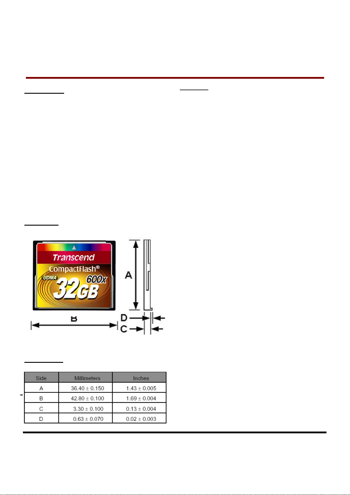
Dimensions
Specification
Transcend Information Inc.
• Durability of Connector: 10,000 times
Built-in 15 bit ECC (Error Correction Code) functionality
•
• Support Global Wear-Leveling to extend product life
• Compliant to CompactFlash, PC Card Mode, and ATA
standards
1
V1.5
T
S
8
G
~
3
2
G
C
F
6
T
S
8
G
~
3
2
T
S
8
G
Interface Specification
Drivers
ATA Compatibility
Physical Specification
Form Factor
Storage Capacities
Dimensions (mm)
~
3
2
G
G
C
C
F
F
6
6
0
0
0
0
0
0
Length
Width
Height
600X CompactFlash Card
No Device Driver Required
ATA/ATAPI 7
PIO Mode 0 - 6
Multiword mode 0 - 4
UDMA Mode 0 - 6
Compact Flash Card
8 GB to 32 GB
36.40 ± 0.15
42.80 ± 0.10
3.30 ± 0.10
Environmental Specifications
℃ to 85 ℃
Operating Temperature
Storage Temperature
Humidity
Operating Humidity (Non condensation)
Storage Humidity (Non condensation)
* Note: 24-hours chamber test on ASUS Striker 2 Extreme, 1GB RAM, Windows® XP Version 2002 SP3.
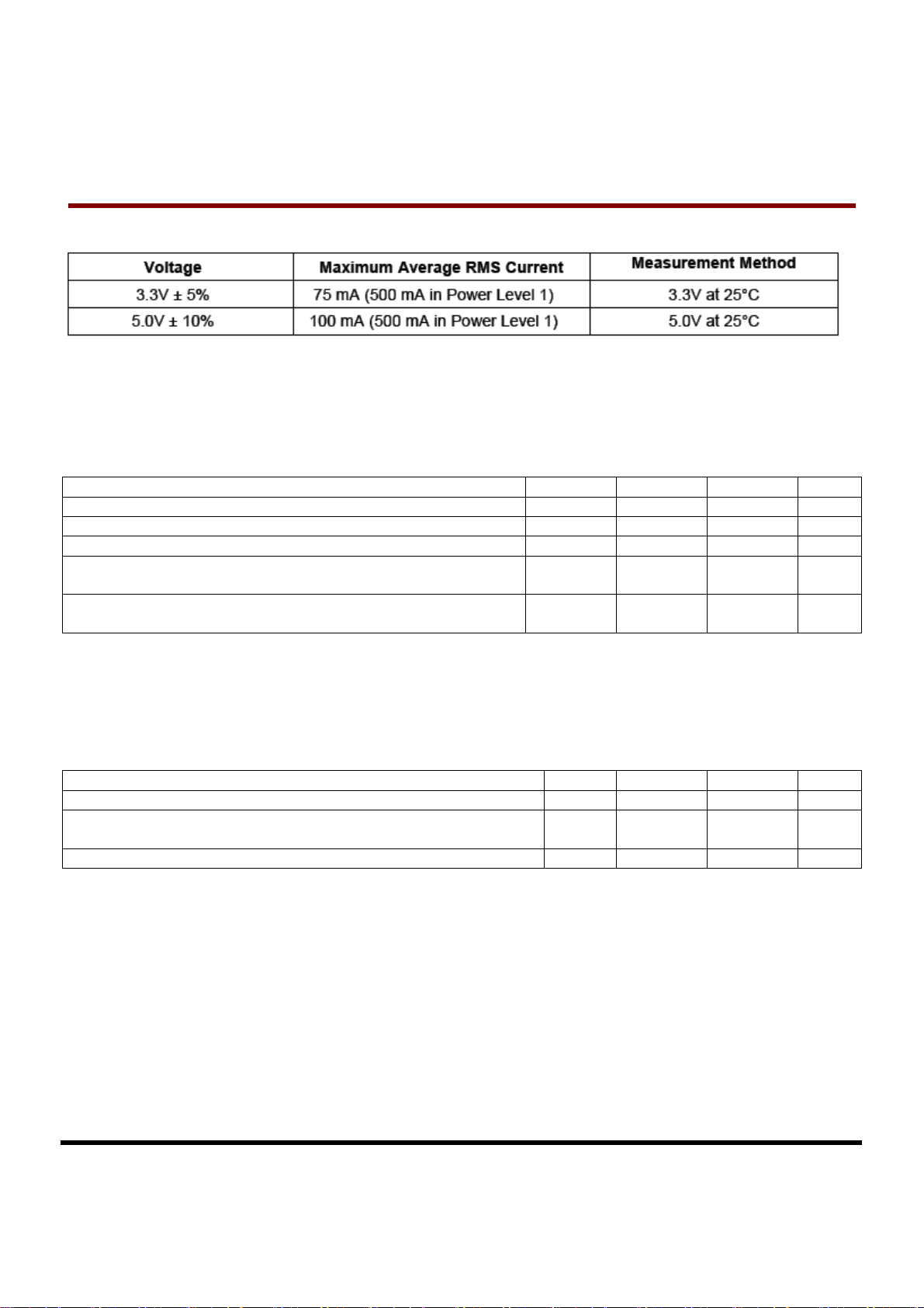
Power Consumption
Product
Power
Consumption
(DC 3.3V
@25℃)
Standby
Read
Write
TS8GCF600 TS16GCF600 TS32GCF600
-25
℃ to 85 ℃
-40
0% to 95%
0% to 95%
2.4mA 2.5mA 2.5mA
222.8mA 232.8mA 233.5mA
218.1mA 211.5mA 231.7mA
Transcend Information Inc.
2
V1.5

T
S
8
G
~
3
2
G
T
S
8
G
T
S
Actual Capacity
* Note: FAT32 format
~
8
G
~
Model P/N User LBA Cylinder Head Sector
TS8GCF600 15662304 15538 16 63
TS16GCF600 31293360 31045 16 63
TS32GCF600 62537328 62041 16 63
3
3
2
2
G
G
C
C
C
F
F
F
6
6
6
0
0
0
0
0
0
600X CompactFlash Card
Transcend
Transcend Information Inc.
3
V1.5
T
S
8
G
~
3
2
G
T
S
8
G
8
G
~
~
T
S
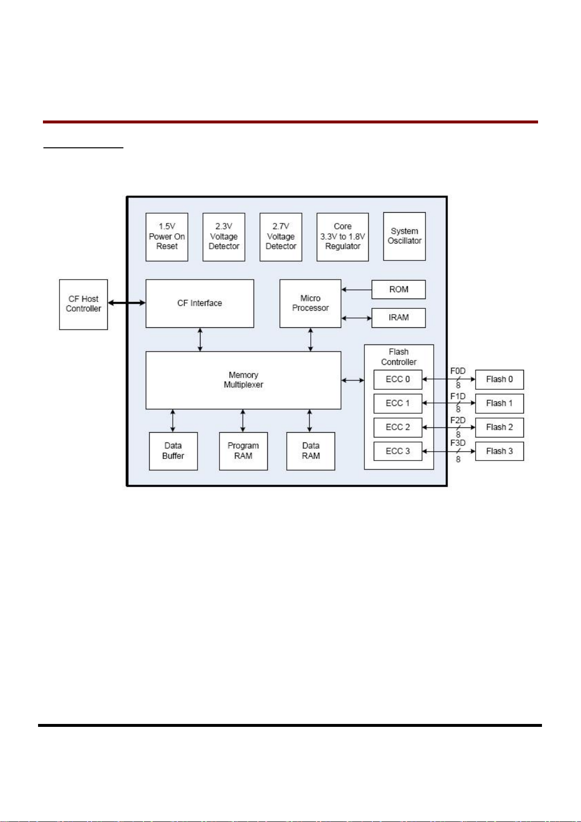
Block Diagram
3
3
2
2
G
G
C
C
C
F
F
F
6
6
6
0
0
0
0
0
0
600X CompactFlash Card
Transcend Information Inc.
4
V1.5
T
T
T
S
S
S
8
8
8
G
G
G
~
~
~
3
3
3
2
2
2
G
G
G
C
C
C
F
F
F
6
6
6
0
0
0
0
0
0
600X CompactFlash Card
Transcend Information Inc.
5
V1.5
T
S
8
G
~
3
2
G
C
F
6
0
0
T
T
S
S
8
8
G
G
~
~
3
3
2
2
G
G
C
C
F
F
6
6
0
0
0
0
600X CompactFlash Card
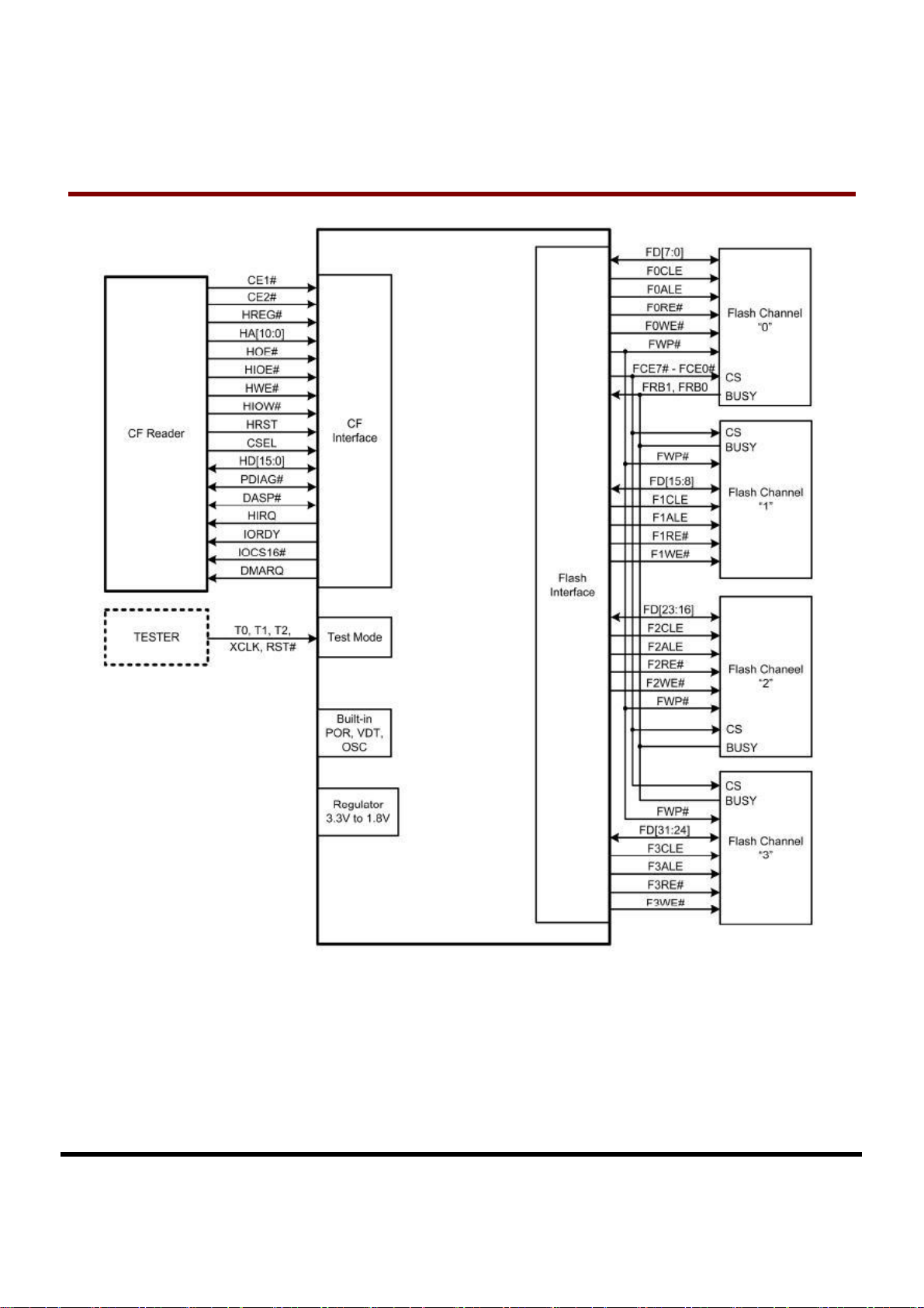
Pin Assignments and Pin Type
PC Card Memory Mode PC Card I/O Mode True IDE Mode4
Pin
Num
1 GND
2 D03 I/O I1Z, OZ3 2 D03 I/O I1Z, OZ3 2 D03 I/O I1Z, OZ3
3 D04 I/O I1Z, OZ3 3 D04 I/O I1Z, OZ3 3 D04 I/O I1Z, OZ3
4 D05 I/O I1Z, OZ3 4 D05 I/O I1Z, OZ3 4 D05 I/O I1Z, OZ3
5 D06 I/O I1Z, OZ3 5 D06 I/O I1Z, OZ3 5 D06 I/O I1Z, OZ3
6 D07 I/O I1Z, OZ3 6 D07 I/O I1Z, OZ3 6 D07 I/O I1Z, OZ3
7 -CE1 I I3U 7 -CE1 I I3U 7 -CS0 I I3Z
8 A10 I I1Z 8 A10 I I1Z 8 A102 I I1Z
9 -OE I I3U 9 -OE I I3U 9 -ATA SEL I I3U
10 A09 I I1Z 10 A09 I I1Z 10 A092 I I1Z
11 A08 I I1Z 11 A08 I I1Z 11 A082 I I1Z
12 A07 I I1Z 12 A07 I I1Z 12 A072 I I1Z
13 VCC
14 A06 I I1Z 14 A06 I I1Z 14 A062 I I1Z
15 A05 I I1Z 15 A05 I I1Z 15 A052 I I1Z
16 A04 I I1Z 16 A04 I I1Z 16 A042 I I1Z
17 A03 I I1Z 17 A03 I I1Z 17 A032 I I1Z
18 A02 I I1Z 18 A02 I I1Z 18 A02 I I1Z
19 A01 I I1Z 19 A01 I I1Z 19 A01 I I1Z
20 A00 I I1Z 20 A00 I I1Z 20 A00 I I1Z
21 D00 I/O I1Z, OZ3 21 D00 I/O I1Z, OZ3 21 D00 I/O I1Z, OZ3
22 D01 I/O I1Z, OZ3 22 D01 I/O I1Z, OZ3 22 D01 I/O I1Z, OZ3
23 D02 I/O I1Z, OZ3 23 D02 I/O I1Z, OZ3 23 D02 I/O I1Z, OZ3
24 WP O OT3 24 -IOIS16 O OT3 24 -IOCS16 O ON3
25 -CD2 O Ground 25 -CD2 O Ground 25 -CD2 O Ground
26 -CD1 O Ground 26 -CD1 O Ground 26 -CD1 O Ground
27 D111 I/O I1Z, OZ3 27 D111 I/O I1Z, OZ3 27 D111 I/O I1Z, OZ3
28 D121 I/O I1Z, OZ3 28 D121 I/O I1Z, OZ3 28 D121 I/O I1Z, OZ3
29 D131 I/O I1Z, OZ3 29 D131 I/O I1Z, OZ3 29 D131 I/O I1Z, OZ3
30 D141 I/O I1Z, OZ3 30 D141 I/O I1Z, OZ3 30 D141 I/O I1Z, OZ3
31 D151 I/O I1Z, OZ3 31 D151 I/O I1Z, OZ3 31 D151 I/O I1Z, OZ3
32 -CE21 I I3U 32 -CE21 I I3U 32 -CS11 I I3Z
33 -VS1 O Ground 33 -VS1 O Ground 33 -VS1 O Ground
Signal
Name
Pin
Type
In, Out Type Pin Num
Ground 1 GND
Power 13 VCC
Signal
Name
Pin
Type
In, Out
Type
Ground 1 GND
Power 13 VCC
Pin
Num
Signal
Name
Pin
Type
In, Out
Type
Ground
Power
Transcend Information Inc.
6
V1.5
T
S
8
G
~
3
2
G
C
F
6
0
0
T
S
8
G
~
3
2
G
C
T
S
8
G
~
3
2
PC Card Memory Mode PC Card I/O Mode True IDE Mode4
Pin
Num
Signal Name
-HIOE
34
HSTROBE
HDMARDY
35
36 -WE I I3U 36 -WE I I3U 36 -WE3 I I3U
37 READY O OT1 37 -IREQ O OT1 37 INTRQ O OZ1
38 VCC Power 38 VCC Power 38 VCC Power
39 -CSEL5 I I2Z 39 -CSEL5 I I2Z 39 -CSEL I I2U
40 -VS2 O OPEN 40 -VS2 O OPEN 40 -VS2 O OPEN
41 RESET I I2Z 41 RESET I I2Z 41 -RESET I I2Z
42
43
44
45 BVD2 O OT1 45 -SPKR O OT1 45 -DASP I/O I1U, ON1
46 BVD1 O OT1 46 -STSCHG O OT1 46 -PDIAG I/O I1U, ON1
47 D081 I/O
48 D091 I/O
49 D101 I/O
50 GND Ground 50 GND Ground 50 GND Ground
-IOWR -IOWR -IOWR7
STOP
-WAIT -WAIT IORDY7 ON1
-DDMARDY
DSTROBE
-INPACK -INPACK
-DMARQ
-REG I I3U 44 -REG
-DMACK
F
G
C
F
10
11
10,11
10
-DDMARDY10 -DDMARDY8
11
12
12
DMACK
6
0
0
6
0
0
Pin
Type
In, Out
Type
I I3U 34
I I3U 35
O OT1 42
O OT1 43
I1Z,
OZ3
I1Z,
OZ3
I1Z,
OZ3
Pin
Num
Signal Name
-HIOE
HSTROBE
-HDMARDY
10,11
STOP
DSTROBE
-DMARQ12
12
47 D081 I/O
48 D091 I/O
1
49 D10
I/O
Pin
Type
10
11
I I3U 34
11
I I3U 35
O OT1 42
O OT1 43 DMARQ O OZ1
I I3U 44 -DMACK
In, Out
Type
I1Z,
OZ3
I1Z,
OZ3
I1Z,
OZ3
600X CompactFlash Card
Pin
Num
Signal Name
-HIOE7
HSTROBE8
-HDMARDY
8,9
STOP
DSTROBE
47 D081 I/O I1Z, OZ3
48 D091 I/O I1Z, OZ3
1
49 D10
I/O I1Z, OZ3
Pin
Type
9
O
9
6
I I3U
In, Out
Type
I I3Z
I I3Z
OT1
13
Note: 1) These signals are required only for 16 bit accesses and not required when installed in 8 bit systems. Devices should allow for 3-state
signals not to consume current.
2) The signal should be grounded by the host.
3) The signal should be tied to VCC by the host.
4) The mode is required for CompactFlash Storage Cards.
5) The -CSEL signal is ignored by the card in PC Card modes. However, because it is not pulled upon the card in these modes,
it should not be left floating by the host in PC Card modes. In these modes, the pin should be connected by the host to PC
Card A25 or grounded by the host.
6) If DMA operations are not used, the signal should be held high or tied to VCC by the host. For proper operation in older hosts: while DMA
operations are not active, the card shall ignore this signal,including a floating condition
7) Signal usage in True IDE Mode except when Ultra DMA mode protocol is active.
8) Signal usage in True IDE Mode when Ultra DMA mode protocol DMA Write is active.
9) Signal usage in True IDE Mode when Ultra DMA mode protocol DMA Read is active.
10) Signal usage in PC Card I/O and Memory Mode when Ultra DMA mode protocol DMA Write is active.
11) Signal usage in PC Card I/O and Memory Mode when Ultra DMA mode protocol DMA Read is active.
12) Signal usage in PC Card I/O and Memory Mode when Ultra DMA protocol is active.
Transcend Information Inc.
7
V1.5
T
S
8
G
~
3
2
G
C
F
6
0
0
T
T
S
S
8
8
G
G
~
~
3
3
2
2
G
G
C
C
F
F
6
6
0
0
0
0
600X CompactFlash Card
Input Leakage Current
Note: In Table 1 below, x refers to the characteristics described in table 2. For example, I1U indicates a pull-up resistor with a type 1
input characteristic.
Table 1: Input Leakage Current
Type Parameter Symbol Conditions MIN TYP MAX Units
IxZ Input Leakage Current IL Vih = Vcc / Vil = Gnd -1
IxU Pull-Up Resistor RPU1 Vcc = 5.0V 50k 500k Ohm
IxD Pull-Down Resistor RPD1 Vcc = 5.0V 50k
Note: The minimum pull-up resistor resistance meets the PCMCIA PC Card specification of 10k ohms but is intentionally higher in the
CompactFlash Specification to reduce power use.
500k Ohm
1 μA
Input Characteristics
Table 2: Input Characteristics
Type Parameter Symbol
Input Voltage
1
CMOS
Input Voltage
2
CMOS
Input Voltage
3
CMOS Schmitt
Trigger
Notes: 1) The host provides a logic output high voltage for a CMOS load of .9 x VCC. For a 5 volt product, this translates to .9 x
4.5 = 4.05 volts minimum Voh.
Vih
Vil
Vih
Vil
Vth
Vtl
MIN TYP MA X MIN TYP MAX
VCC = 3.3 V VCC = 5.0 V
2.4
1.5
1.8
1.0
0.6 4.0
0.6 2.0
1
2.8
2.0
0.8
0.8
Units
Volts
Volts
Volts
Output Drive Type
Note: In Table 3 below, x refers to the characteristics described in Table 4. For example, OT3 refers to Totem pole output with a type 3
output drive characteristic.
Type Output Type Valid Conditions
OTx Totempole Ioh & Iol
OZx Tri-State N-P Channel Ioh & Iol
OPx P-Channel Only Ioh Only
ONx N-Channel Only Iol Only
Transcend Information Inc.
Table 3: Output Drive Type
8
V1.5
T
S
8
G
~
3
2
G
C
F
6
0
0
T
S
8
G
~
3
2
G
C
T
S
8
G
~
3
2
Output Drive Characteristics
Type Parameter Symbol Conditions MIN TYP MAX Units
1 Output Voltage
2 Output Voltage
3 Output Voltage
X
F
G
C
F
Tri-State Leakage
Current
6
6
0
0
0
0
Table 4: Output Drive Characteristics
Voh
Vol
Voh
Vol
Voh
Vol
Ioz
Ioh = -4 mA
Iol = 4 mA
Ioh = -4 mA
Iol = 4 mA
Ioh = -4 mA
Iol = 4 mA
Vol = Gnd
Voh = Vcc
Vcc
-0.8V
Vcc
-0.8V
Vcc
-0.8V
-10
600X CompactFlash Card
Gnd
Volts
+0.4V
Volts
Gnd
+0.4V
Volts
Gnd
+0.4V
10 μA
Transcend Information Inc.
9
V1.5

T
S
8
G
~
3
2
G
C
F
6
0
0
6
6
0
0
0
0
T
T
S
S
8
8
G
G
~
~
3
3
2
2
G
G
C
C
F
F
Signal Description
Signal Name Dir. Pin Description
600X CompactFlash Card
A10 – A00
(PC Card Memory Mode)
A10 – A00
(PC Card I/O Mode)
A02 - A00
(True IDE Mode)
BVD1
(PC Card Memory Mode)
-STSCHG
(PC Card I/O Mode)
Status Changed
-PDIAG
(True IDE Mode)
BVD2
(PC Card Memory Mode)
-SPKR
(PC Card I/O Mode)
-DASP
(True IDE Mode)
I
8,10,11,12,
14,15,16,17,
18,19,20
I
I/O 46 This signal is asserted high, as BVD1 is not supported.
I/O 45 This signal is asserted high, as BVD2 is not supported.
18,19,20
These address lines along with the -REG signal are used to select the following:
The I/O port address registers within the CompactFlash Storage Card , the
memory mapped port address registers within the CompactFlash Storage Card,
a byte in the card's information structure and its configuration control and status
registers.
This signal is the same as the PC Card Memory Mode signal.
In True IDE Mode, only A[02:00] are used to select the one of eight registers
in the Task File, the remaining address lines should be grounded by the host.
This signal is asserted low to alert the host to changes in the READY and Write
Protect states, while the I/O interface is configured. Its use is controlled by the
Card Config and Status Register.
In the True IDE Mode, this input / output is the Pass Diagnostic signal in the
Master / Slave handshake protocol.
This line is the Binary Audio output from the card. If the Card does not support
the Binary Audio function, this line should be held negated.
In the True IDE Mode, this input/output is the Disk Active/Slave Present signal in
the Master/Slave handshake protocol.
-CD1, -CD2
(PC Card Memory Mode)
-CD1, -CD2
(PC Card I/O Mode)
-CD1, -CD2
(True IDE Mode)
O 26,25 These Card Detect pins are connected to ground on the CompactFlash Storage
Transcend Information Inc.
Card. They are used by the host to determine that the CompactFlash Storage
Card is fully inserted into its socket.
This signal is the same for all modes.
This signal is the same for all modes.
10
V1.5

T
S
8
G
~
3
2
G
C
F
6
0
0
6
6
0
0
0
0
T
T
S
S
8
8
G
G
~
~
3
3
2
2
G
G
C
C
F
F
Signal Name Dir. Pin Description
-CE1, -CE2
(PC Card Memory Mode)
Card Enable
-CE1, -CE2
(PC Card I/O Mode)
Card Enable
-CS0, -CS1
(True IDE Mode)
I 7,32
These input signals are used both to select the card and to indicate to the card
whether a byte or a word operation is being performed. -CE2 always accesses
the odd byte of the word.-CE1 accesses the even byte or the Odd byte of the
word depending on A0 and -CE2. A multiplexing scheme based on A0,-CE1,
-CE2 allows 8 bit hosts to access all data on D0-D7. See Table 27, Table 29,
Table 31, Table 35, Table 36 and Table 37.
This signal is the same as the PC Card Memory Mode signal.
In the True IDE Mode, -CS0 is the address range select for the task file
registers while -CS1 is used to select the Alternate Status Register and the
Device Control Register.
While –DMACK is asserted, -CS0 and –CS1 shall be held negated and the
width of the transfers shall be 16 bits.
600X CompactFlash Card
-CSEL
(PC Card Memory Mode)
-CSEL
(PC Card I/O Mode)
-CSEL
(True IDE Mode)
D15 - D00
(PC Card Memory Mode)
D15 - D00
(PC Card I/O Mode)
D15 - D00
(True IDE Mode)
GND
(PC Card Memory Mode)
GND
(PC Card I/O Mode)
GND
(True IDE Mode)
I 39 This signal is not used for this mode, but should be connected by the host to PC
Card A25 or grounded by the host.
This signal is not used for this mode, but should be connected by the host to PC
Card A25 or grounded by the host.
This internally pulled up signal is used to configure this device as a Master or a
Slave when configured in the True IDE Mode.
When this pin is grounded, this device is configured as a Master.
When the pin is open, this device is configured as a Slave.
31,30,29,28,
I/O
27,49,48,47,
6,5,4,3,2,
23, 22, 21
-- 1,50 Ground.
These lines carry the Data, Commands and Status information between the host
and the controller. D00 is the LSB of the Even Byte of the Word. D08 is the LSB
of the Odd Byte of the Word.
This signal is the same as the PC Card Memory Mode signal.
In True IDE Mode, all Task File operations occur in byte mode on the low order
bus D[7:0] while all data transfers are 16 bit using D[15:0].
This signal is the same for all modes.
This signal is the same for all modes.
Transcend Information Inc.
11
V1.5

T
S
8
G
~
3
2
G
C
F
6
0
0
T
S
8
G
~
3
2
G
C
T
S
8
G
~
3
2
Signal Name Dir. Pin Description
G
C
F
F
6
6
0
0
0
0
600X CompactFlash Card
-INPACK
(PC Card Memory Mode except
Ultra DMA Protocol Active)
-INPACK
(PC Card I/O Mode except Ultra
DMA Protocol Active)
Input Acknowledge
-DMARQ
(PC Card Memory Mode -Ultra
DMA Protocol Active)
-DMARQ
(PC Card I/O Mode -Ultra DMA
Protocol Active)
DMARQ
(True IDE Mode)
-HIOE
(PC Card Memory Mode except
Ultra DMA Protocol Active)
-HIOE
(PC Card I/O Mode except Ultra
DMA Protocol Active)
-HIOE
(True IDE Mode – Except Ultra
DMA Protocol Active)
-HDMARDY
(All Modes - Ultra DMA Protocol
DMA Read)
HSTROBE
(All Modes - Ultra DMA Protocol
DMA Write)
O 43 This signal is not used in this mode.
The Input Acknowledge signal is asserted by the CompactFlash Storage Card
when the card is selected and responding to an I/O read cycle at the address that
is on the address bus. This signal is used by the host to control the enable of any
input data buffers between the CompactFlash Storage Card and the CPU.
Hosts that support a single socket per interface logic, such as for Advanced
Timing Modes and Ultra DMA operation may ignore the –INPACK signal from the
device and manage their input buffers based solely on Card Enable signals.
This signal is a DMA Request that is used for DMA data transfers between host
and device. It shall be asserted by the device when it is ready to transfer data to
or from the host. For Multiword DMA transfers, the direction of data transfer is
controlled by -HIOE and -IOWR. This signal is used in a handshake manner with
(-)DMACK, i.e., the device shall wait until the host asserts (-)DMACK before
negating (-)DMARQ, and re-asserting (-)DMARQ if there is more data to
transfer.
In PCMCIA I/O Mode, the
performing an I/O Read cycle to the device. The host shall not initiate an I/O
Read cycle while
In True IDE Mode, DMARQ shall not be driven when the device is not selected in
the Drive-Head register.
While a DMA operation is in progress, -CS0 (-CE1)and -CS1 (-CE2) shall be held
negated and the width of the transfers shall be 16 bits.
If there is no hardware support for True IDE DMA mode in the host, this output
signal is not used and should not be connected at the host. In this case, the BIOS
must report that DMA mode is not supported by the host so that device drivers
will not attempt DMA mode operation.
A host that does not support DMA mode and implements both PC Card and True
IDE modes of operation need not alter the PC Card mode connections while in
True IDE mode as long as this does not prevent proper operation in any mode.
I 34 This signal is not used in this mode.
This is an I/O Read strobe generated by the host. This signal gates I/O data onto
the bus from the CompactFlash Storage Card when the card is configured to use
the I/O interface.
In True IDE Mode, while Ultra DMA mode is not active, this signal has the same
function as in PC Card I/O Mode.
In all modes when Ultra DMA mode DMA Read is active, this signal is asserted
by the host to indicate that the host is ready to receive Ultra DMA data-in bursts.
The host may negate – HDMARDY to pause an Ultra DMA transfer.
In all modes when Ultra DMA mode DMA Write is active, this signal is the data
out strobe generated by the host. Both the rising and falling edge of HSTROBE
cause data to be latched by the device. The host may stop generating
HSTROBE edges to pause an Ultra DMA data-out burst.
-DMARQ is asserted by the device.
-DMARQ shall be ignored by the host while the host is
Transcend Information Inc.
12
V1.5

T
S
8
G
~
3
2
G
C
F
6
0
0
T
S
8
G
~
3
2
G
C
T
S
8
G
~
3
2
Signal Name Dir. Pin Description
-IOWR
(PC Card Memory Mode– Except
Ultra DMA Protocol Active)
-IOWR
(PC Card I/O Mode –Except Ultra
DMA Protocol Active)
-IOWR
(True IDE Mode – Except Ultra
DMA Protocol Active)
STOP
(All Modes – Ultra DMA Protocol
Active)
-OE
(PC Card Memory Mode)
-OE
(PC Card I/O Mode)
-ATA SEL
(True IDE Mode)
READY
(PC Card Memory Mode)
-IREQ
(PC Card I/O Mode)
INTRQ
(True IDE Mode)
G
C
F
F
6
6
0
0
0
0
I 35
I 9
O 37
This signal is not used in this mode.
The I/O Write strobe pulse is used to clock I/O data on the Card Data bus into the
CompactFlash Storage Card controller registers when the CompactFlash
Storage Card is configured to use the I/O interface.
The clocking shall occur on the negative to positive edge of the signal (trailing
edge).
In True IDE Mode, while Ultra DMA mode protocol is not active, this signal has
the same function as in PC Card I/O Mode. When Ultra DMA mode protocol is
supported, this signal must be negated before entering Ultra DMA mode
protocol.
In All Modes, while Ultra DMA mode protocol is active, the assertion of this signal
causes the termination of the Ultra DMA data burst.
This is an Output Enable strobe generated by the host interface. It is used to read
data from the CompactFlash Storage Card in Memory Mode and to read the CIS
and configuration registers.
In PC Card I/O Mode, this signal is used to read the CIS and configuration
registers.
To enable True IDE Mode this input should be grounded by the host.
In Memory Mode, this signal is set high when the CompactFlash Storage Card is
ready to accept a new data transfer operation and is held low when the card is
busy.
At power up and at Reset, the READY signal is held low (busy) until the
CompactFlash Storage Card has completed its power up or reset function. No
access of any type should be made to the CompactFlash Storage Card during
this time.
Note, however, that when a card is powered up and used with RESET
continuously disconnected or asserted, the Reset function of the RESET pin is
disabled. Consequently, the continuous assertion of RESET from the application
of power shall not cause the READY signal to remain continuously in the busy
state.
I/O Operation – After the CompactFlash Storage Card Card has been configured
for I/O operation, this signal is used as -Interrupt Request. This line is strobed
low to generate a pulse mode interrupt or held low for a level mode interrupt.
In True IDE Mode signal is the active high Interrupt Request to the host.
600X CompactFlash Card
Transcend Information Inc.
13
V1.5

T
S
8
G
~
3
2
G
C
F
6
0
0
T
S
8
G
~
3
2
G
C
T
S
8
G
~
3
2
Signal Name Dir. Pin Description
-REG
(PC Card Memory Mode– Except
Ultra DMA Protocol Active)
Attribute Memory Select
-REG
(PC Card I/O Mode –Except Ultra
DMA Protocol Active)
-DMACK
(PC Card Memory Mode when
Ultra DMA Protocol Active)
DMACK
(PC Card I/O Mode when Ultra
DMA Protocol Active)
-DMACK
(True IDE Mode)
G
C
F
F
6
6
0
0
0
0
I 44
This signal is used during Memory Cycles to distinguish between Common
Memory and Register (Attribute) Memory accesses. High for Common Memory,
Low for Attribute Memory.
In PC Card Memory Mode, when Ultra DMA Protocol is supported by the host
and the host has enabled Ultra DMA protocol on the card the, host shall keep the
-REG signal negated during the execution of any DMA Command by the device.
The signal shall also be active (low) during I/O Cycles when the I/O address is on
the Bus.
In PC Card I/O Mode, when Ultra DMA Protocol is supported by the host and the
host has enabled Ultra DMA protocol on the card the, host shall keep the -REG
signal asserted during the execution of any DMA Command by the device.
This is a DMA Acknowledge signal that is asserted by the host in response to
(-)DMARQ to initiate DMA transfers.
In True IDE Mode, while DMA operations are not active, the card shall ignore the
(-)DMACK signal, including a floating condition.
If DMA operation is not supported by a True IDE Mode only host, this signal
should be driven high or connected to VCC by the host.
A host that does not support DMA mode and implements both PC Card and
True-IDE modes of operation need not alter the PC Card mode connections
while in True-IDE mode as long as this does not prevent proper operation all
modes.
600X CompactFlash Card
RESET
(PC Card Memory Mode)
RESET
(PC Card I/O Mode)
-RESET
(True IDE Mode)
VCC
(PC Card Memory Mode)
VCC
(PC Card I/O Mode)
VCC
(True IDE Mode)
I 41 The CompactFlash Storage Card is Reset when the RESET pin is high with the
following important exception:
The host may leave the RESET pin open or keep it continually high from the
application of power without causing a continuous Reset of the card. Under
either of these conditions, the card shall emerge from power-up having
completed an initial Reset.
The CompactFlash Storage Card is also Reset when the Soft Reset bit in the
Card Configuration Option Register is set.
This signal is the same as the PC Card Memory Mode signal.
In the True IDE Mode, this input pin is the active low hardware reset from the
host.
-- 13,38 +5 V, +3.3 V power.
This signal is the same for all modes.
This signal is the same for all modes.
Transcend Information Inc.
14
V1.5

T
S
8
G
~
3
2
G
C
F
6
0
0
T
S
8
G
~
3
2
G
C
T
S
8
G
~
3
2
Signal Name Dir. Pin Description
-VS1
-VS2
(PC Card Memory Mode)
-VS1
-VS2
(PC Card I/O Mode)
-VS1
-VS2
(True IDE Mode)
-WAIT
(PC Card Memory Mode – Except
Ultra DMA Protocol Active)
-WAIT
(PC Card I/O Mode –Except Ultra
DMA Protocol Active)
IORDY
(True IDE Mode – Except Ultra
DMA Protocol Active)
-DDMARDY
(All Modes – Ultra DMA Write
Protocol Active)
DSTROBE
(All Modes – Ultra DMA Read
Protocol Active)
G
C
F
F
6
6
0
0
0
0
O 33
40
O 42
Voltage Sense Signals. -VS1 is grounded on the Card and sensed by the Host so
that the CompactFlash Storage Card CIS can be read at 3.3 volts and -VS2 is
reserved by PCMCIA for a secondary voltage and is not connected on the Card.
This signal is the same for all modes.
This signal is the same for all modes.
The -WAIT signal is driven low by the CompactFlash Storage Card to signal the
host to delay completion of a memory or I/O cycle that is in progress.
This signal is the same as the PC Card Memory Mode signal.
In True IDE Mode, except in Ultra DMA modes, this output signal may be used as
IORDY.
In all modes, when Ultra DMA mode DMA Write is active, this signal is asserted
by the device during a data burst to indicate that the device is ready to receive
Ultra DMA data out bursts. The device may negate -DDMARDY to pause an
Ultra DMA transfer.
In all modes, when Ultra DMA mode DMA Read is active, this signal is the data in
strobe generated by the device. Both the rising and falling edge of DSTROBE
cause data to be latched by the host. The device may stop generating
DSTROBE edges to pause an Ultra DMA data in burst.
600X CompactFlash Card
-WE
(PC Card Memory Mode)
-WE
(PC Card I/O Mode)
-WE
(True IDE Mode)
WP
(PC Card Memory Mode)
Write Protect
-IOIS16
(PC Card I/O Mode)
-IOCS16
(True IDE Mode)
I 36 This is a signal driven by the host and used for strobing memory write data to the
O 24
Transcend Information Inc.
registers of the CompactFlash Storage Card when the card is configured in the
memory interface mode. It is also used for writing the configuration registers.
In PC Card I/O Mode, this signal is used for writing the configuration registers.
In True IDE Mode, this input signal is not used and should be connected to VCC
by the host.
Memory Mode – The CompactFlash Storage Card does not have a write protect
switch. This signal is held low after the completion of the reset initialization
sequence.
I/O Operation – When the CompactFlash Storage Card is configured for I/O
Operation Pin 24 is used for the -I/O Selected is 16 Bit Port (-IOIS16) function. A
Low signal indicates that a 16 bit or odd byte only operation can be performed at
the addressed port.
In True IDE Mode this output signal is asserted low when this device is expecting
a word data transfer cycle.
15
V1.5
T
S
8
G
~
3
2
G
C
F
6
0
0
T
T
S
S
8
8
G
G
~
~
3
3
2
2
G
G
C
C
F
F
6
6
0
0
0
0
600X CompactFlash Card
Electrical Specification
The following tables indicate all D.C. Characteristics for the CompactFlash Storage Card. Unless
otherwise stated, conditions are:
Vcc = 5V ±10%
Vcc = 3.3V ± 5%
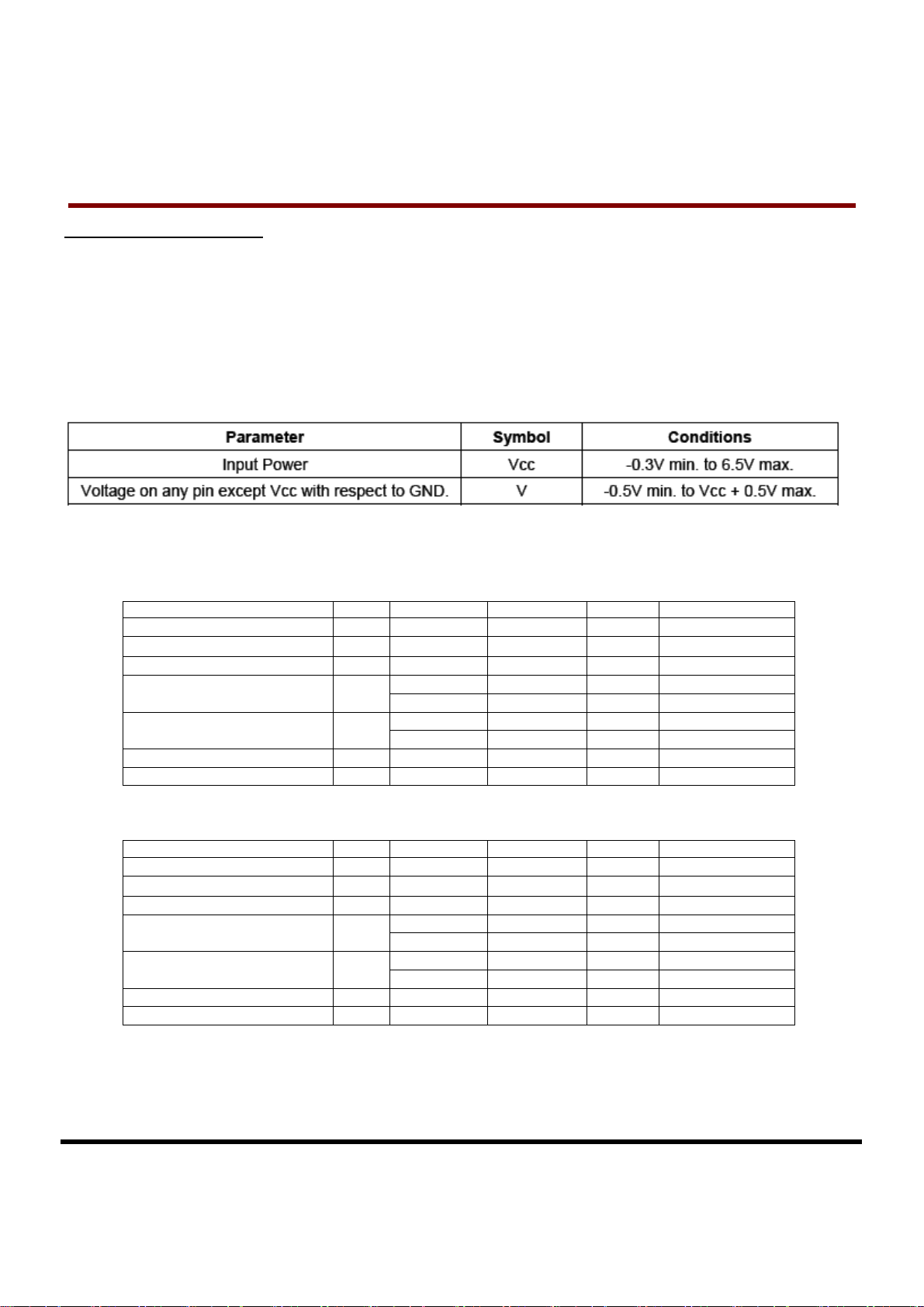
Absolute Maximum Conditions
DC Characteristics
CompactFlash Interface I/O at 5.0V
Parameter Symbol Min. Max. Unit Remark
Supply Voltage V
High level output voltage VOH
Low level output voltage VOL 0.8 V
High level input voltage VIH
Low level input voltage VIL
Pull up resistance2 R
Pull down resistance RPD 50 97 KOhm
4.5 5.5 V
CC
─ 0.8
V
CC
4.0 V
2.92 V
0.8 V
1.70 V
50 73 KOhm
PU
V
Non-schmitt trigger
Non-schmitt trigger
Schmitt trigger
Schmitt trigger
1
1
CompactFlash Interface I/O at 3.3V
Parameter Symbol Min. Max. Unit Remark
Supply Voltage V
High level output voltage VOH
Low level output voltage VOL 0.8 V
High level input voltage VIH
Low level input voltage VIL
Pull up resistance2 R
Pull down resistance RPD 47.5 172 KOhm
1. Include CE1, CE2, HREG, HOE, HIOE, HWE, HIOW pins
2. Include CE1, CE2, HREG, HOE, HIOE, HWE, HIOW, CSEL (P35), PDIAG, DASP pins
Transcend Information Inc.
3.135 3.465 V
CC
─ 0.8
V
CC
2.4 V
2.05 V
0.6 V
1.25 V
52.7 141 KOhm
PU
16
V
Non-schmitt trigger
Schmitt trigger
Non-schmitt trigger
Schmitt trigger
1
1
V1.5
T
S
8
G
~
3
2
G
C
F
6
0
0
T
S
8
G
~
3
2
T
S
8
G
Input Power
~
3
2
G
G
C
C
F
F
6
6
0
0
0
0
600X CompactFlash Card
Input Characteristics for UDMA mode >4
In UDMA modes greater than 4, the following characteristics apply. Voltage output high and low values shall be met
at the source connector to include the effect of series termination.
Table: Input Characteristics (UDMA Mode > 4)
Parameter Symbol MIN MAX Units
DC supply voltage to drivers V
Low to high input threshold V+ 1.5 2.0 Volts
High to low input threshold V- 1.0 1.5 Volts
Difference between input thresholds:
((V+
current value
Average of thresholds:
((V+
current value
) - (V-
) + (V-
current value
current value
))
))/2
3.3 –8% 3.3% + 8% Volts
DD3
V
320 Volts
HYS
V
1.3 1.7 Volts
THRAVG
Output Drive Characteristics for UDMA mode > 4
In UDMA modes greater than 4, the characteristics specified in the following table apply. Voltage output high and low
values shall be met at the source connector to include the effect of series termination.
Table: Output Drive Characteristics (UDMA Mode > 4)
Parameter Symbol MIN MAX Units
DC supply voltage to drivers V
Voltage output high at -6 mA to +3 mA (at VoH2 the output shall be
able to supply and sink current toVDD3)
Voltage output low at 6 mA V
Notes:
1) I
oLDASP shall be 12 mA minimum to meet legacy timing and signal integrity.
2) I
oH value at 400 μ A is insufficient in the case of DMARQ that is pulled low by a 5.6 kΩ resistor.
3) Voltage output high and low values shall be met at the source connector to include the effect of series termination.
4) A device shall have less than 64 μ A of leakage current into a 6.2 KΩ pull-down resistor while the INTRQ signal is in the released
state.
3.3 –8% 3.3% + 8% Volts
DD3
V
V
oH2
0.51 Volts
oL2
–0.51 V
DD3
+0.3 Volts
DD3
Transcend Information Inc.
17
V1.5
T
S
8
G
~
3
2
G
C
F
6
0
0
T
T
S
S
8
8
G
G
~
~
3
3
2
2
G
G
C
C
F
F
6
6
0
0
0
0
600X CompactFlash Card
Signal Interface
Electrical specifications shall be maintained to ensure data reliability. Additional requirements are necessary for
Advanced Timing Modes and Ultra DMA modes operations. See next sections for additional information.
Item Signal Card
Control Signal
Status Signal
-CE1
-CE2
-REG
-HIOE
-IOWR
-OE
-WE
RESET
READY
-WAIT
WP
-INPACK
Pull-up to V
shall be sufficient to keep inputs inactive
when the pins are not connected at the
1
host.
Pull-up to V
Pull-up to V
10
Host
500 KΩ≧ R≧ 50 KΩ and
CC
500 KΩ ≧ R ≧ 50 KΩ .
CC
500 KΩ ≧ R ≧ 50 KΩ .
CC
10
1,2
1,2,9,
Pull-up to V
In PCMCIA PC Card modes Pull-up to V
R ≧ 10 KΩ .
In True IDE mode, if DMA operation is
supported by the host, Pull-down to Gnd R
≧ 5.6 KΩ .
PC Card / True IDE hosts switch the pull-up
to pull down in True IDE mode if DMA
operation is supported.
The PC Card mode Pull-up may be left
active during True IDE mode if True IDE
DMA operation is not supported.
R ≧ 10 KΩ .
CC
4
5
3
CC
Address
Data Bus D[15:00]
Card Detect -CD[2:1] Connected to GND in the card
Voltage Sense
Battery/Detect BVD[2:1]
A[10:00]
-CSEL
-VS1
-VS2
1.
Pull-up to Vcc 10 KΩ ≦ R ≦ 100KΩ .
Pull-up R ≧ 50 KΩ .
3.6
Notes: 1) Control Signals: each card shall present a load to the socket no larger than 50 pF 10 at a DC current of 700 μ A low
state and 150 μ A high state, including pull-resistor. The socket shall be able to drive at least the following load
10 while meeting all AC timing requirements: (the number of sockets wired in parallel) multiplied by (50 pF with
DC current 700 μ A low state and 150 μ A high state per socket).
2) Resistor is optional.
3) Status Signals: the socket shall present a load to the card no larger than 50 pF
Transcend Information Inc.
18
10 at a DC current of 400 μ A low
V1.5

T
S
8
G
~
3
2
G
C
F
6
0
0
T
S
8
G
~
3
2
G
C
T
S
8
G
~
3
2
4) Status Signals: the socket shall present a load to the card no larger than 50 pF
5) Status Signals: the socket shall present a load to the card no larger than 50 pF
6) BVD2 was not defined in the JEIDA 3.0 release. Systems fully supporting JEIDA release 3 SRAM cards shall
7) Address Signals: each card shall present a load of no more than 100pF
8) Data Signals: the host and each card shall present a load no larger than 50pF
9) Reset Signal: This signal is pulled up to prevent the input from floating when a CFA to PCMCIA adapter is used in
10) Host and card restrictions for CF Advanced Timing Modes and Ultra DMA modes: Additional Requirements for
Additional Requirements for CF Advanced Timing Modes
The CF Advanced Timing modes include PC Card I/O and Memory modes that are 100ns or faster, PC Card Ultra
DMA modes 3 or above and True IDE PIO Modes 5,6, Multiword DMA Modes 3,4 and True IDE Ultra DMA modes
3 or above.
When operating in CF Advanced timing modes, the host shall conform to the following requirements:
F
G
C
F
state and 100 μ A high state, including pull-up resistor. The card shall be able to drive at least the following load
10 while meeting all AC timing requirements: 50 pF at a DC current of 400 μ A low state and 100 μ A high state.
state and 100 μ A high state, including pull-up resistor. The card shall be able to drive at least the following load
10 while meeting all AC timing requirements: 50 pF at a DC current of 400 μ A low state and 100 μ A high state.
state and 100 μ A high state, including pull-up resistor. The card shall be able to drive at least the following load
10 while meeting all AC timing requirements: 50 pF at a DC current of 400 μ A low state and 1100 μ A high state.
pull-up pin 45 (BVD2) to avoid sensing their batteries as “Low.”
150μ A high state. The host shall be able to drive at least the following load
requirements: (the number of sockets wired in parallel) multiplied by (100pF with DC current 450μ A low state
and 150μ A high state per socket).
150μ A high state. The host and each card shall be able to drive at least the following load
timing requirements: 100pF with DC current 1.6mA low state and 300μ A high state. This permits the host to wire
two sockets in parallel without derating the card access speeds.
a PCMCIA revision 1 host. However, to minimize DC current drain through the pull-up resistor in normal
operation the pull-up should be turned off once the Reset signal has been actively driven low by the host.
Consequently, the input is specified as an I2Z because the resistor is not necessarily detectable in the input
current leakage test.
CF Advanced Timing Modes and Ultra DMA Electrical Requirements for additional required limitations on the
implementation of CF Advanced Timing modes and Ultra DMA modes respectively.
6
6
0
0
0
0
10 at a DC current of 450μ A low state and
600X CompactFlash Card
10 at a DC current of 400 μ A low
10 at a DC current of 400 μ A low
10 while meeting all AC timing
10 at a DC current of 450μ A and
10 while meeting all AC
1) Only one CF device shall be attached to the CF Bus.
2) The host shall not present a load of more than 40pF to the device for all signals, including any cabling.
3) The maximum cable length is 0.15 m (6 in). The cable length is measured from the card connector to the host
controller. 0.46 m (18 in) cables are not supported.
4) The -WAIT and IORDY signals shall be ignored by the host.
Devices supporting CF Advanced timing modes shall also support slower timing modes, to ensure operability with
systems that do not support CF Advanced timing modes
Transcend Information Inc.
19
V1.5
T
S
8
G
~
3
2
G
C
F
6
0
0
T
S
8
G
~
3
2
G
C
T
S
8
G
~
3
2
Ultra DMA Electrical Requirements
¾ Host and Card signal capacitance limits for Ultra DMA operation
The host interface signal capacitance at the host connector shall be a maximum of 25 pF for each signal as measured at
1 MHz.
The card interface signal capacitance at the card connector shall be a maximum of 20 pF for each signal as measured at
1 MHz.
¾ Series termination required for Ultra DMA operation
Series termination resistors are required at both the host and the card for operation in any of the Ultra DMA modes. Table
describes typical values for series termination at the host and the device.
F
G
C
F
6
6
0
0
0
0
600X CompactFlash Card
Table: Typical Series Termination for Ultra DMA
Signal Host Termination Device Termination
-HIOE (-HDMARDY,HSTROBE) 22 ohm 82 ohm
-IOWR (STOP) 22 ohm 82 ohm
-CS0, -CS1 33 ohm 82 ohm
A00, A01, A02 33 ohm 82 ohm
-DMACK 22 ohm 82 ohm
D15 through D00 33 ohm 33 ohm
DMARQ 82 ohm 22 ohm
INTRQ 82 ohm 22 ohm
IORDY (-DDMARDY, DSTROBE) 82 ohm 22 ohm
-RESET 33 ohm 82 ohm
NOTE − Only those signals requiring termination are listed in this table. If a signal is not listed, series
termination is not required for operation in an Ultra DMA mode. Shows signals also requiring a pull-up or
pull-down resistor at the host. The actual termination values should be selected to compensate for transceiver
and trace impedance to match the characteristic cable impedance.
Transcend Information Inc.
20
V1.5
T
T
T
S
S
S
8
8
8
G
G
G
~
~
~
3
3
3
2
2
2
G
G
G
C
C
C
F
F
F
6
6
6
0
0
0
0
0
0
600X CompactFlash Card
Table: Ultra DMA Termination with Pull-up or Pull down Example
¾ Printed Circuit Board (PCB) Trace Requirements for Ultra DMA
On any PCB for a host or device supporting Ultra DMA:
9 The longest D[15:00] trace shall be no more than 0.5" longer than either STROBE trace as measured from the
IC pin to the connector.
9 The shortest D[15:00] trace shall be no more than 0.5" shorter than either STROBE trace as measured from
the IC pin to the connector.
¾ Ultra DMA Mode Cabling Requirement
Operation in Ultra DMA mode requires a crosstalk suppressing cable. The cable shall have a grounded line
9
between each signal line.
9
For True IDE mode operation using a cable with IDE (ATA) type 40 pin connectors it is recommended that the
host sense the cable type using the method described in the ANSI INCITS 361-2002 AT Attachment - 6
standard, to prevent use of Ultra DMA with a 40 conductor cable.
Transcend Information Inc.
21
V1.5
T
S
8
G
~
3
2
G
C
F
6
0
0
T
S
8
G
~
3
2
G
C
T
S
8
G
~
3
2
Attribute Memory Read Timing Specification
Attribute Memory access time is defined as 300 ns. Detailed timing specs are shown in Table below
Speed Version 300 ns
Read Cycle Time tc(R) tAVAV 300
Address Access Time ta(A) tAVQV 300
Card Enable Access Time ta(CE) tELQV 300
Output Enable Access Time ta(OE) tGLQV 150
Output Disable Time from CE tdis(CE) tEHQZ 100
Output Disable Time from OE tdis(OE) tGHQZ 100
Address Setup Time tsu (A) tAVGL 30
Output Enable Time from CE ten(CE) tELQNZ 5
Output Enable Time from OE ten(OE) tGLQNZ 5
Data Valid from Address Change tv(A) tAXQX 0
Note: All times are in nanoseconds. Dout signifies data provided by the CompactFlash Storage Card to the system. The -CE signal or
both the -OE signal and the -WE signal shall be de-asserted between consecutive cycle operations.
F
G
C
F
Item Symbol IEEE Symbol Min ns. Max ns.
6
6
0
0
0
0
600X CompactFlash Card
Transcend Information Inc.
22
V1.5

T
S
8
G
~
3
2
G
C
F
6
0
0
T
S
8
G
~
3
2
G
C
T
S
8
G
~
3
2
Configuration Register (Attribute Memory) Write Timing Specification
The Card Configuration write access time is defined as 250 ns. Detailed timing specifications are shown in Table
below.
G
C
F
F
6
0
0
6
0
0
Table: Configuration Register (Attribute Memory) Write Timing
600X CompactFlash Card
Speed Version
Item Symbol Min ns Max ns
Write Cycle Time tc(W) 250
Write Pulse Width tw(HWE) 150
Address Setup Time tsu(HA) 30
Write Recovery Time trec(HWE) 30
Data Setup Time for WE tsu(HD-HWEH) 80
Data Hold Time th(HD) 30
Note: All times are in nanoseconds. Din signifies data provided by the system to the CompactFlash Storage Card .
250 ns
Transcend Information Inc.
23
V1.5
T
S
8
G
~
3
2
G
C
F
6
0
0
T
S
8
G
~
3
2
G
C
T
S
8
G
~
3
2
Common Memory Read Timing Specification
F
G
C
F
Item Symbol
6
6
0
0
0
0
Cycle Time Mode: 250 ns 120 ns 100 ns 80 ns
IEEE
Symbol
600X CompactFlash Card
Min
Max
Min
ns.
ns.
Max
ns.
ns.
Min
ns.
Max
ns.
Min
ns.
Max
ns.
Output Enable Access Time ta(HOE) tGLQV
Output Disable Time from HOE tdis(HOE) tGHQZ
Address Setup Time tsu(HA) tAVGL 30
Address Hold Time th(HA) tGHAX 20
CEx Setup before HOE tsu(CEx) tELGL 5
CEx Hold following HOE th(CEx) tGHEH 20
Wait Delay Falling from HOE tv(IORDY-HOE) tGLWTV
Data Setup for Wait Release tv(IORDY) tQVWTH
Wait Width Time2 tw(IORDY) tWTLWTH 350
Notes:1) –WAIT is not supported in this mode.
2) The maximum load on -WAIT is 1 LSTTL with 50 pF (40pF below 120nsec Cycle Time) total load. All times are in
nanoseconds. Dout signifies data provided by the CompactFlash Storage Card to the system. The -WAIT signal may be ignored
if the -OE cycle to cycle time is greater than the Wait Width time. The Max Wait Width time can be determined from the Card
Information Structure. The Wait Width time meets the PCMCIA PC Card specification of 12µs but is intentionally less in this
specification.
125
100
35
0
15
15
5
15
60
60
35
0
350
10
15
5
15
50
50
35
0
350
10
10
10
45
45
5
1
na
1
na
1
na
Transcend Information Inc.
24
V1.5
T
S
8
G
~
3
2
G
C
F
6
0
0
6
6
0
0
0
0
T
T
S
S
8
8
G
G
~
~
3
3
2
2
G
G
C
C
F
F
Common Memory Write Timing Specification
Cycle Time Mode: 250 ns 120 ns 100 ns 80 ns
Item Symbol
Data Setup before HWE tsu (HD-HWEH) tDVWH 80
Data Hold following HWE th(HD) tWMDX 30
HWE Pulse Width tw(HWE) tWLWH 150
Address Setup Time tsu(HA) tAVWL 30
CEx Setup before HWE tsu(CEx) tELWL 5
Write Recovery Time trec(HWE) tWMAX 30
Address Hold Time th(HA) tGHAX 20
CEx Hold following HWE th(CEx) tGHEH 20
Wait Delay Falling from HWE tv (IORDY-HWE) tWLWTV
WE High from Wait Release tv(IORDY) tWTHWH 0
Wait Width Time2 tw (IORDY) tWTLWTH
IEEE
Symbol
Min
ns.
Max
ns.
35
350
600X CompactFlash Card
Min
Max
Min
Max
ns.
ns.
ns.
ns.
50
15
70
15
5
15
15
15
0
350
35
40
10
60
10
5
15
15
15
0
35
350
Min
ns.
30
10
55
10
5
15
15
10
na
Max
ns.
1
na
1
1
na
Notes: 1) –WAIT is not supported in this mode.
2) The maximum load on -WAIT is 1 LSTTL with 50 pF (40pF below 120nsec Cycle Time) total load. All times are in
nanoseconds. Din signifies data provided by the system to the CompactFlash Storage Card. The -WAIT signal may be
ignored if the -HWE cycle to cycle time is greater than the Wait Width time. The Max Wait Width time can be determined
from the Card Information Structure. The Wait Width time meets the PCMCIA PC Card specification of 12μs but is
intentionally less in this specification.
Transcend Information Inc.
25
V1.5
T
S
8
G
~
3
2
G
C
F
6
0
0
T
S
8
G
~
3
2
G
C
T
S
8
G
~
3
2
I/O Input (Read) Timing Specification
G
C
F
F
6
6
0
0
0
0
600X CompactFlash Card
Cycle Time Mode: 250 ns 120 ns 100 ns 80 ns
Item Symbol
Data Delay after HIOE td(HIOE) tlGLQV
Data Hold following HIOE th(HIOE) tlGHQX 0
HIOE Width Time tw(HIOE) tlGLIGH 165
Address Setup before HIOE tsuA(HIOE) tAVIGL 70
Address Hold following HIOE thA(HIOE) tlGHAX 20
CEx Setup before HIOE tsuCE(HIOE) tELIGL 5
CEx Hold following HIOE thCE(HIOE) tlGHEH 20
HREG Setup before HIOE tsuREG (HIOE) tRGLIGL 5
HREG Hold following HIOE thREG (HIOE) tlGHRGH 0
Wait Delay Falling from HIOE2 tdWT(HIOE) tlGLWTL 35
Data Delay from Wait Rising2 td(IORDY) tWTHQV
Wait Width Time2 tw(IORDY) tWTLWTH
IEEE
Symbol
Min
ns.
Max
ns.
100
0
350
Min
Max
ns.
50
5
70
25
10
5
10
5
0
Min
Max
Min
Max
ns.
ns.
ns.
ns.
ns.
50
5
65
25
10
5
10
5
0
35 35 Na
0 0 Na
350 350 Na
5
55
15
10
5
10
5
0
45
1
1
1
Transcend Information Inc.
26
V1.5
T
S
8
G
~
3
2
G
C
F
6
0
0
T
S
8
G
~
3
2
G
C
T
S
8
G
~
3
2
I/O Output (Write) Timing Specification
Data Setup before HIOW tsu(HIOW) tDVIWH 60 20 20 15
Data Hold following HIOW th(HIOW) tlWHDX 30 10 5 5
HIOW Width Time tw(HIOW) tlWLIWH 165 70 65 55
Address Setup before HIOW tsuA(HIOW) tAVIWL 70 25 25 15
Address Hold following HIOW thA(HIOW) tlWHAX 20 20 10 10
CEx Setup before HIOW tsuCE (HIOW) tELIWL 5 5 5 5
CEx Hold following HIOW thCE (HIOW) tlWHEH 20 20 10 10
HREG Setup before HIOW tsuREG (HIOW) tRGLIWL 5 5 5 5
HREG Hold following HIOW thREG (HIOW) tlWHRGH 0 0 0 0
Wait Delay Falling from HIOW2 tdWT(HIOW) tlWLWTL 35 35 35 Na1
HIOW high from Wait high2 tdrHIOW (IORDY) tWTJIWH 0 0 0 Na1
Wait Width Time2 tw(IORDY) tWTLWTH 350 350 350 Na1
F
G
C
F
Item Symbol
6
6
0
0
0
0
Cycle Time Mode: 255 ns 120 ns 100 ns 80 ns
IEEE
Symbol
Min
ns.
Max
ns.
600X CompactFlash Card
Min
ns.
Max
ns.
Min
ns.
Max
ns.
Min
ns.
Max
ns.
Transcend Information Inc.
27
V1.5
 Loading...