

Specifications*
General
Power Supply DC 12V (11V - 16V),
Test Voltage 13.2V
Negative Ground
Current Consumption Less than 2.5A
Power Output 17W×4 (1kHz, 1%, 4Ω)
LW/MW Radio
Frequency Range 153 - 279kHz (LW)
522 - 1,611kHz (MW)
Usable Sensitivity 32dB(µV) (S/N 20dB)
Signal Noise Ratio More than 42dB
FM Stereo Radio
Frequency Range 87.5 - 108MHz
Usable Sensitivity 6dB(µV) (S/N 30dB)
Signal Noise Ratio More than 30dB
CQ-MS0370K
AM/FM/RDS MPX Radio with CD Player
TOYOTA PART No. : 86120-0D140
ID CODE : W53806
VEHICLE : Yaris
DESTINATION : Europe
PRODUCED AFTER : Dec., 2002
RDS Radio
RDS Sensitivity 22dB(µV) (S/N 30dB)
CD Player
Decoding 16bit (Linear)
Channel Separation 65dB (IHF-A)
Signal Noise Ratio More than 70dB (IHF-A)
Dimensions** 178×50×165mm (W×H×D)
Weight** 1.48kg
* Specifications and the design are subject to possible modification
without notice due to improvements.
** Dimensions and Weight shown are approximate.
CQ-MS0370K
CONTENTS
Page Page
1 FEATUERS 2
2 LASER PRODUCTS
3 SYSTEM BLOCK DIAGRAM
4 FRONT VIEW AND FUNCTIONS
5 REAR VIEW AND CONNECTORS
6 WIRING CONNECTION
7 BLOCK DIAGRAM
8 TERMINALS DESCRIPTION
9 PACKAGE AND IC BLOCK DIAGRAM 10
2
10 REPLACEMENT PARTS LIST
2
11 EXPLODED VIEW (Unit)
12 CD PLAYER PARTS
3
3
13 EXPLODE D VIEW (CD Deck)
4
14 WIRING DIAGRAM
15 SCHEMATIC DIAGRAM
5
7
16 MEMO
12
17
18
19
20
25
27
1 FEATUERS
PLL (Phase Locked Loop) synthesized tuning.
·
24-station preset (6-AM, 18-FM).
·
RDS radio.
·
CD changer control function.
·
Emergency Eject function.
·
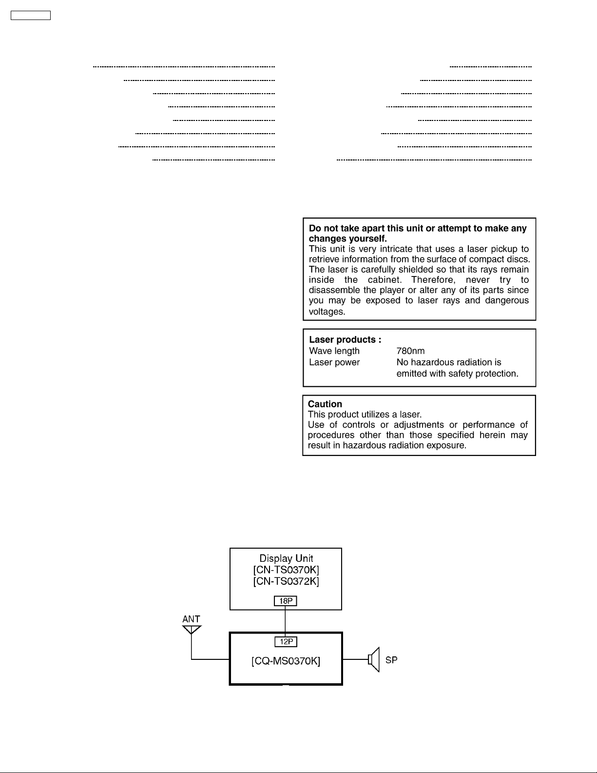
2 LASER PRODUCTS
3 SYSTEM BLOCK DIAGRAM
2
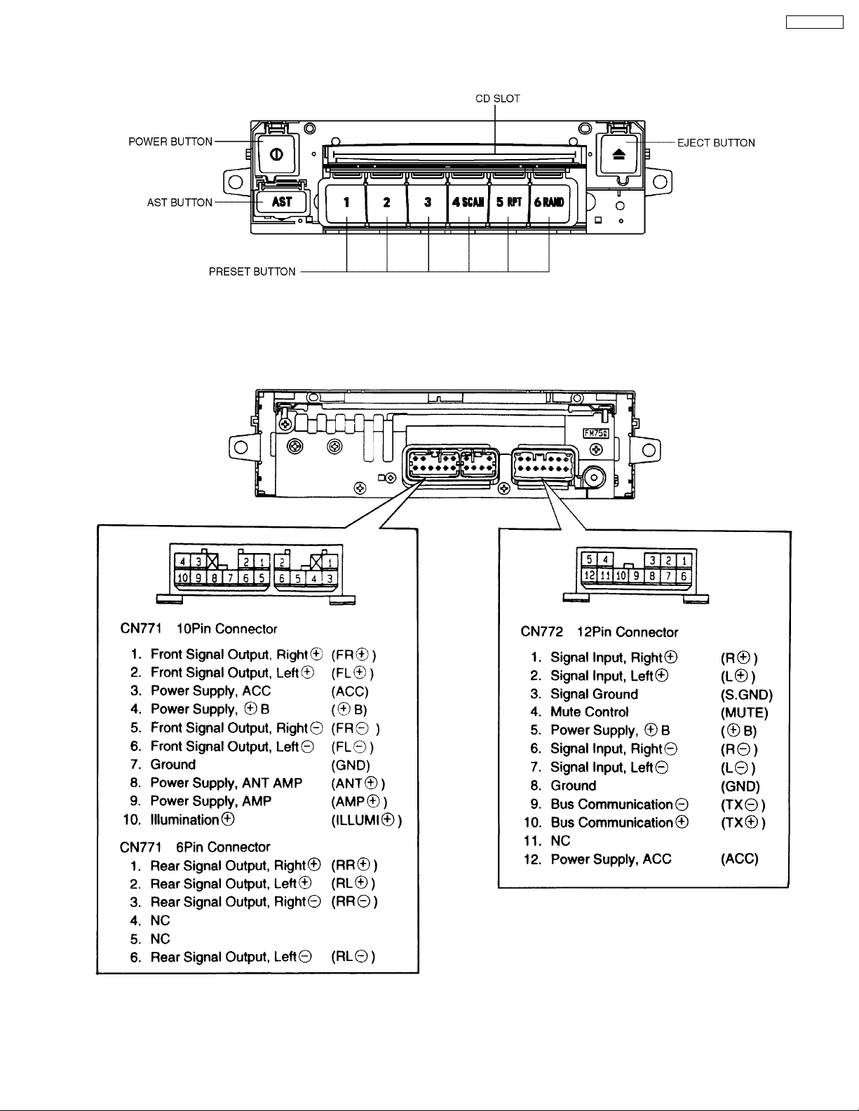
4 FRONT VIEW AND FUNCTIONS
5 REAR VIEW AND CONNECTORS
CQ-MS0370K
3
CQ-MS0370K
6 WIRING CONNECTION
4
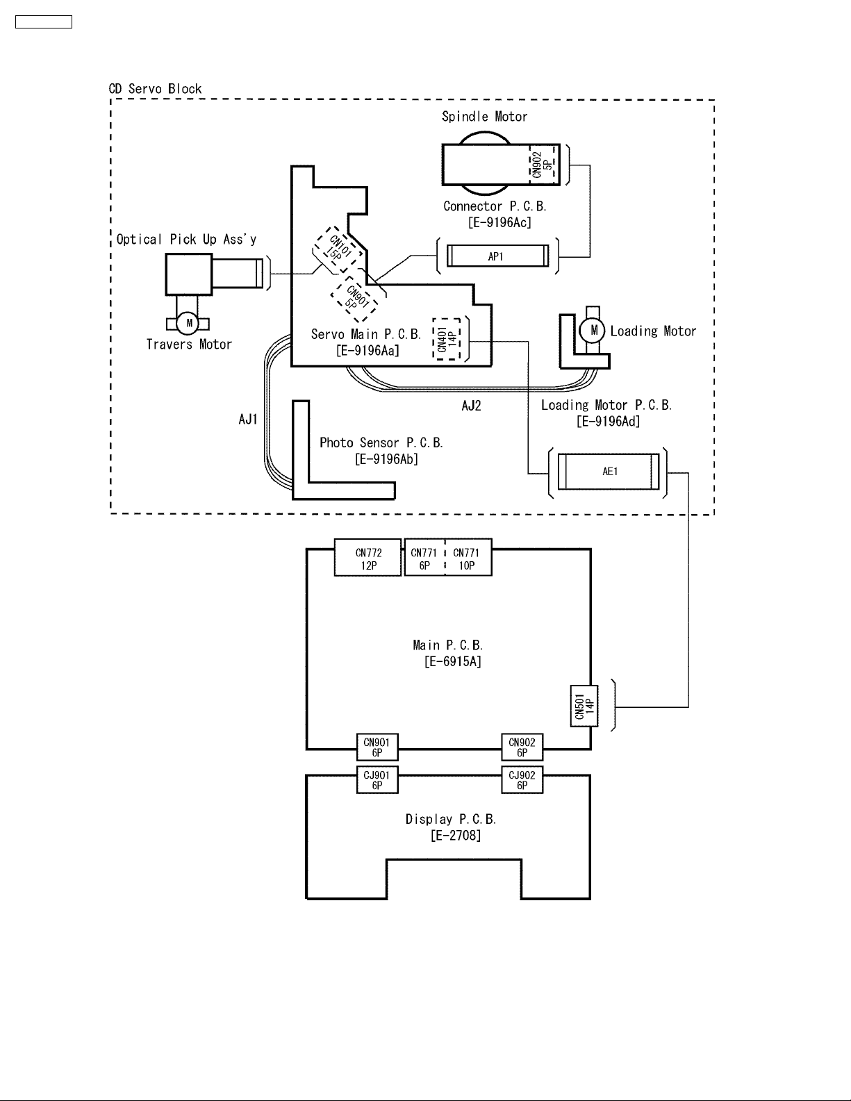
7 BLOCK DIAGRAM
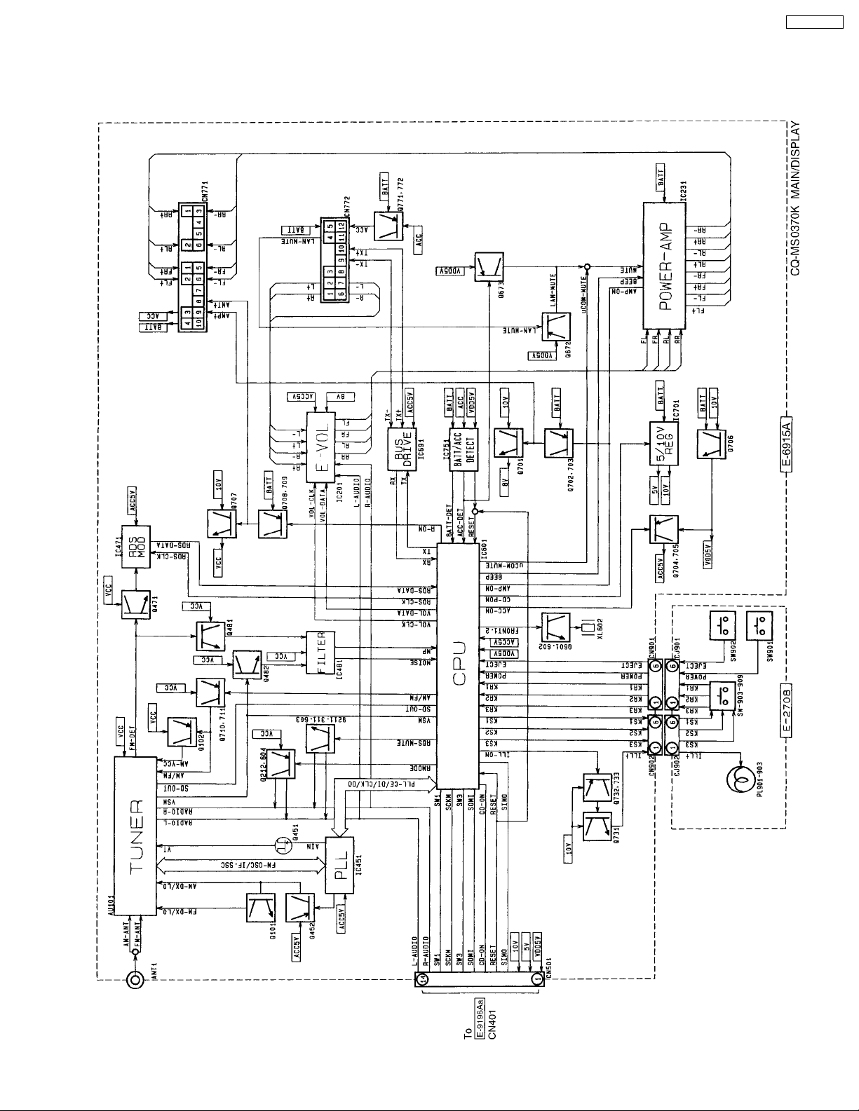
7.1. Main / Display Block
CQ-MS0370K
5
CQ-MS0370K
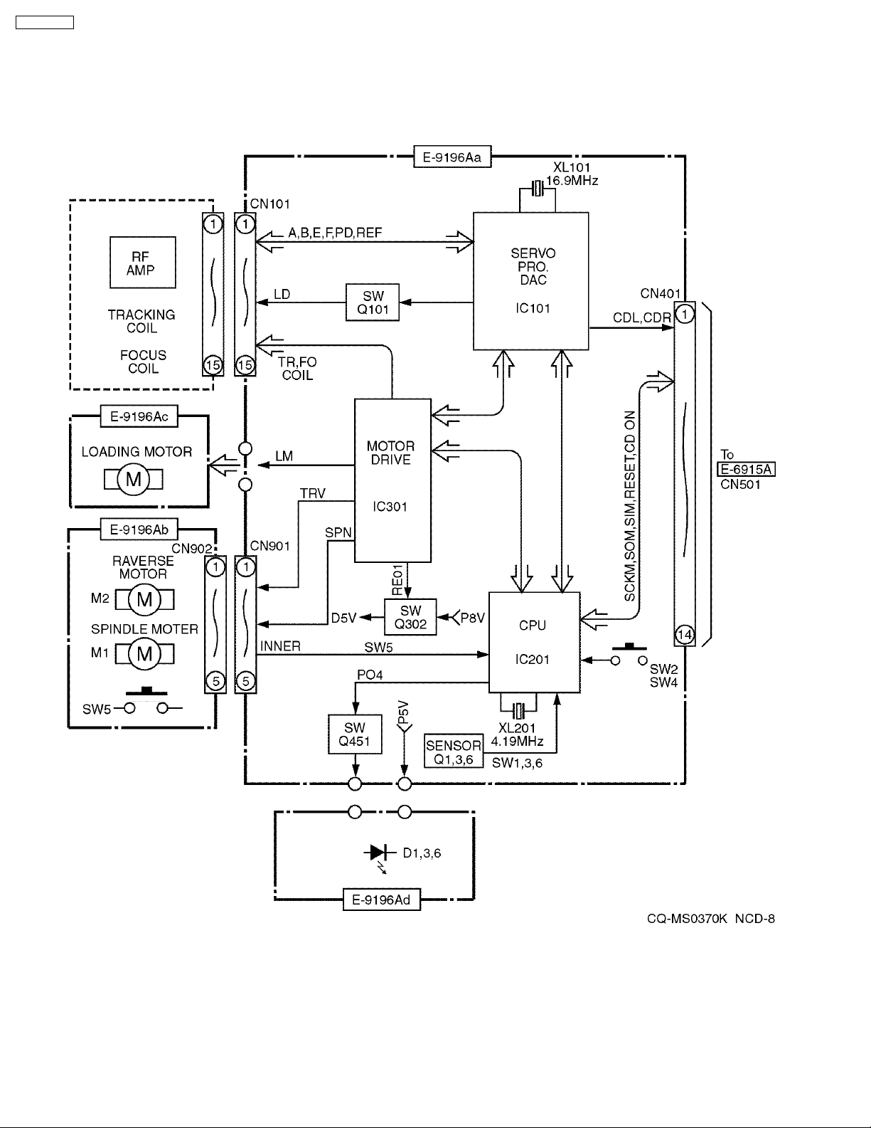
7.2. CD Servo Block
6
8 TERMINALS DESCRIPTION
CQ-MS0370K
8.1. Main Block
Pin
No.
1 MUTE Audio mute O 0
2 ILL-ON Illuni. power control O 5
3 ACC-ON ACC power control O 5
4 AMP-ON AMP power control O 5
5 CD.P.ON CD power control O 5
6 CD-RESET CD reset O 5
7 CD-ON CD ON signal O 5
8 CD-SCKM Data shift clock O 5
9 CD-SOM Serial data input I 3.5
10 CD-SIM Serial data output O 3.6
11 RESET System reset I 4.7
12 XT2 Crystal oscillator I 3.1
13 XT1 Crystal oscillator O 2.8
14 VSS Ground - 0
15 X2 Crystal oscillator I 3.2
16 X1 Crystal oscillator O 3
17 REGOFF (Connecting to VDD) - 5
18 REGC (Connecting to VDD) - 5
19 VDD +5V power supply - 5
20 FCONT2 Frequency control O 5
21 FCONT1 Frequency control O 0
22 (NC) No connection - 23 (NC) No connection - 24 (NC) No connection - 25 (NC) No connection - 26 (NC) No connection - 27 (NC) No connection - 28 (NC) No connection - 29 (NC) No connection - 30 SW1 Disc in SW O 4.8
31 SW3 Disc out SW O 4.8
32 LCD-CE Not used - 33 LCD-CLK Not used - 34 LCD-DI Not used - 35 LCD-DO Not used - 36 (NC) No connection - 37 (NC) - - 38 SEEK-SD/VC (Connecting to GND) - 0
39 IF (Connecting to GND) - 0
40 VSS Ground - 0
41 VDD +5V power supply - 5
42 (NC) No connection - 43 KS4 Not used - 44 KS3 Key scan signal O 2.1
45 KS2 Key scan signal O 2.2
46 KS1 Key scan signal O 2.2
47 (NC) No connection - 48 KR3 Key return signal I 0
49 KR2 Key return signal I 0
50 KR1 Key return signal I 0
51 (NC) No connection - 52 POWER Power SW I 5
53 (NC) No connection - 54 PLL-DO PLL data input I 2.5
55 PLL-CLK PLL clock O 0
56 PLL-DI PLL data output O 0
57 PLL-CE PLL chip enabl O 0
58 (NC) No connection - 59 (NC) No connection - 60 (NC) No connection - 61 (NC) No connection - -
Port Description I/O (V)
IC601 : C2CBHF000054
Pin
No.
62 (NC) No connection - 63 (NC) No connection - 64 (NC) No connection - 65 RDS-CLK RDS clock O 3.2
66 RDS-DATA RDS data I 3.5
67 (NC) No connection - 68 RMODE Radio mode selection O 5
69 SD.ST B/S detection I 5
70 (NC) No connection - 71 (NC) No connection - 72 (NC) No connection - 73 TESTMODE (Connecting to GND) - 0
74 VSM Radio signal strength I 0
75 MP I 0
76 NOISE Noise level detection I 0.6
77 (NC) No connection - 78 RDS-MUTE RDS mute O 0
79 TEST (VDD pull-up) I 5
80 VOL CLK Electronic volume clock O 0
81 VOL DATA Electronic volume data O 0
82 AVDD Analog power supply - 5
83 AVREF1 Analog reference voltage - 5
84 AVSS Ground - 0
85 RX AVC-LAN data I 0
86 TX AVC-LAN data O 0
87 (NC) (Connecting to GND) - 0
88 (NC) (Connecting to GND) - 0
89 (NC) (Connecting to VDD) - 5
90 +B DET Battery level detection I 5
91 (NC) (Connecting to VDD) - 6.5
92 ACC-DET ACC level detection I 5
93 EJECT CD eject SW I 5
94 (NC) (Connecting to VDD) - 5
95 (NC) No connection - 96 FM/AM AM/FM mode selection O 5
97 R.ON Radio power on O 5
98 (NC) No connection - 99 BEEP Beep sound I 0
100 (NC) No connection - -
Port Description I/O (V)
7
CQ-MS0370K
8.2. CD Servo Block
Pin
No.
1 D.GND Digital GND - 0
2 RFOK RFOK signal O 4.9
3 /RST Reset I 5.1
4 A0 Command/parameter
5 /STB Data strobing I 5.1
6 /SCK Clock signal I 3.7
7 SO Serial data output O 0.8
8 SI Serial data input I 3.2
9 /XTALEN Crystal oscillator control I 0
10 D.VDD Digital VDD - 5
11 DA.VDD DA converter VDD - 5
12 ROUT Rch audio output AO 2.6
13 DA.GND DA converter GND - 0
14 REGC External capacitor for SCF
15 DA.GND DA converter GND - 0
16 LOUT Lch audio output AO 2.6
17 DA.DVV DA converter VDD - 5
18 R+ Rch+ PWM output O 19 R- Rch- PWM output O 20 L- Lch- PWM output O 21 L+ Lch+ PWM output O 22 X.VDD Crystal oscillator VDD - 5
23 /XTAL Crystal oscillator O 0
24 XTAL Crystal oscillator I 2.6
25 X.GND Crystal oscillator GND - 0
26 D.VDD Digital VDD - 5
27 EMPH Preemphasis information O 5
28 FLAG Flag output O 0
29 DIN Serial data input I 2.6
30 DOUT Cereal audio data output O 2.6
31 SCKIN Cereal clock input I 2.6
32 SCKO - O 2.6
33 LRCKIN LRCK signal I 2.6
34 LRCK LR identification O 2.6
35 HOLD/WDCK - O 0
36 TX - - 37 D.GND Digital GND - 0
38 C16M - - 39 LIMIT - I 0
40 D.VDD Digital VDD - 5
41 LOCK EFM synchronous detection O 5
42 RFCK Frame synchronization O 2.6
43 MIRR/WFCK - O 0
44 PLCK Bit clock monitor O 2.6
45 D.GND Digital GND - 0
46 C1D1 C1 error correction O 0
47 C1D2 C1 error correction O 0
48 C2D1 C2 error correction O 0
49 C2D2 C2 error correction O 0
50 C2D3 C2 error correction O 0
51 D.VDD Digital VDD - 5
52 PACK PAC synchronization of CD-
53 TSO Serial output of CD-TEXT O 0
54 TSI Serial input of CD-TEXT I 0
55 /TSCK Cereal clock input of CD-TEXT I 0
56 TSTB Parameter strobing signal of
57 D.GND Digital GND - 0
58 TEST0 Test I 0
59 TEST1 Test I 0
60 ATEST Test AO 0
Port Description I/O (V)
IC101 : C1BB00000414
identification
regulator
TEXT
CD-TEXT
I 3.9
A- 2.7
O 1.8
I 0
Pin
No.
61 A.GND Analog GND - 2.6
62 FD Foci drive AO 0
63 TD Tracking drive AO 2.6
64 SD Thread drive AO 2.6
65 MD Spindle drive AO 2.6
66 DAC0 - - 67 DAC1 - AO 2.6
68 DAC2 - AO 2.6
69 DAC3 - - 70 A.VDD Analog +5V Power Supply - 5
71 EFM E FM signal output O 2.6
72 ASY Reference voltage input of EFM
73 C3T For 3T detection A- 3
74 RFI RF signal for EFM data
75 AGCO RF signal output after gain
76 AGCI RF-AGC amplifier input AI 2.6
77 RFO RF Samingamp output AO 2.8
78 EQ2 - - 79 EQ1 Equalizer connection of RF
80 RF- RF Samingamp reversing input AI 2.4
81 A.GND Analog GND - 0
82 A Photodetector A input AI 2.6
83 C Photodetector C input AI 2.6
84 B Photodetector B input AI 2.6
85 D Photodetector D input AI 2.7
86 F Photodetector F input AI 2.7
87 E Photodetector E input AI 2.6
88 A.VDD Analog VDD - 5
89 REFOUT Reference potential output AO 2.5
90 FE- Focus error amplifier reversing
91 FEO Focus error amplifier output AO 2.5
92 TE- Tracking error amplifier
93 TEO Tracking error amplifier output AO 2.5
94 TE2 Tracking error output after it
95 TEC Tracking comparator input AI 2.5
96 A.GND Analog GND - 0
97 PD PD detection signal input AI 0
98 LD LD controlling current output AO 3
99 PN APC control electrode setting I 0
100 A.VDD Analog VDD - 5
Port Description I/O (V)
AI 2.6
comparator
AI 2.6
generation
AO 2.6
adjusted
A- 2.7
amplifier
AI 2.5
input
AI 2.6
reversing input
AO 2.6
amplifies
8
Pin
Port Description I/O (V)
No.
1 A0 Address output O 3.8
2 /RST Reset O 5.1
3 RFOK RFOK signal I 4.9
4 /PS2 IC301 mute O 5.1
5 /PC1 IC301 mute O 0
6 TRV Traverse motor control O 2.5
7 LOD Loading motor control O 2.5
8 PS2 Connected test pin (PS2) - 0
9 PC1 Connected test pin (PC1) - 5.1
10 PC Connected test pin (PC) - 0
11 IFR Connected GND - 0
12 NC Connected test pin (TP12) - 0.6
13 VPP Connected GND - 0
14 X2 Crystal oscillator - 3.3
15 X1 Crystal oscillator - 2.9
16 VSS GND - 0
17 VDD +5V power supply - 5.1
18 /RESET Reset input I 5.1
19 TP19 Connected test pin (TP19) - 0
20 TP20 Connected test pin (TP20) - 0
21 TP21 Connected test pin (TP21) - 0
22 AMUTE(NC) - - 23 CDON CD power supply ON I 5.0
24 INTP1 Connected GND - 0
25 INTP0 Connected GND - 0
26 SIMO Serial data output I 0
27 SOMI Serial data input O 2.9
28 SCKM Shift clock (Serial data) I 5.0
29 Q1 SW1 Disk insertion sensor signal I 4.6
30 Q3 SW3 Disk preseting sensor signal I 4.6
31 Q6 SW6 Preliminary sensor I 4.7
32 SW4 Disk clamp I 0
33 SW5 Inner SW I 4.9
34 SW2 Feeder Arm I 5.1
35 TP35 Connected test pin (TP35) - 0
36 TP36 - - 0
37 TP37 Connected test pin (TP37) - 0.5
38 VDD +5V power supply - 5.1
39 VSS GND - 0
40 /XEN XEN signal O 0
41 SI Serial data input O 3.1
42 SO Serial data output I 0.7
43 /SCK Shift clock O 3.6
44 /STB Strobing O 5.0
IC201 : C2BBFD000403
CQ-MS0370K
9
 Loading...