

Toyota CQ-ES7880AZ Schematic
Specifications*
CQ-ES7880AZ
AM/FM/MPX ELECTRONIC TUNING
RADIO with 6-Disc CD Changer
PART No. : 86120-02860
ID CODE : 52831
VEHICLE : Corolla
DESTINATION : Brazil
PRODUCED AFTER : Mar., 2008
General
Power Supply DC 12V (10.5V - 16V),
Test Voltage 13.2V
Negative Ground
Current Consumption 3A or less (at illumi on)
Dark Current 0.3mA or less
AM Radio
Frequency Range 530-1,620kHz (5kHz steps)
Effective Sensitivity 32dB/µV or less
Signal to Noise Ratio 45dB or more (15kHz LPF)
FM Radio
Frequency Range 87.9-108.0MHz (100kHz steps)
Effective Sensitivity 16dB/µV or less (15kHz LPF)
Signal to Noise Ratio 50dB or more (15kHz LPF)
CD Changer (YGFD53316)
Signal to Noise Ratio 65dB or more (IHF-A)
Channel Separation 60dB or more (1kHz BPF)
Total Harmonic Distortion 0.2% or less (30kHz LPF, 400Hz HPF)
Dimensions* 178 x 100 x 149.5mm (W x H x D)
Weight** 2.5kg
* Specifications and the design are subject to possible modification
without notice due to improvements.
** Dimensions and Weight shown are approximate.
CQ-ES7880AZ
CONTENTS
Page Page
1 ABOUT LEAD FREE SOLDER (PbF) 2
2 FEATURES
3 SYSTEM BLOCK DIAGRAM (For Testing)
4 VIEWS AND FUNCTIONS
5 WIRING CONNECTION
6 BLOCK DIAGRAM
7 TERMINALS DESCRIPTION
8 PACKAGE AND IC BLOCK DIAGRAM 8
2
9 REPLACEMENT PARTS LIST
2
10 EXPLODE D VIEW (Unit)
11 WIRING DIAGRAM
3
4
12 SCHEMATIC DIAGRAM
5
13 MEMO
6
11
18
19
23
27
1 ABOUT LEAD FREE
SOLDER (PbF)
Distinction of PbF PCB:
· PCBs (manufactured) using lead free solder will have a
PbF stamp on the PCB.
Caution :
· Pb free solder has a higher melting point than standard
solder; Typically the melting point is 50 - 70°F (30 40°C) higher. Please use a soldering iron with
temperature control and adjust it to 700 ± 20°F (370 ±
10°C). In case of using high temperature soldering iron,
please be careful not to heat too long.
· Pb free solder will tend to splash when heated too high
(about 1100°F/600°C).
2 FEATURES
· PLL (Phase Locked Loop) synthesized tuning
· MP3/WMA playback from CD-R/RW
· ALPS Tuner Pack (Digital Tuner)
· Illumination Color-Amber
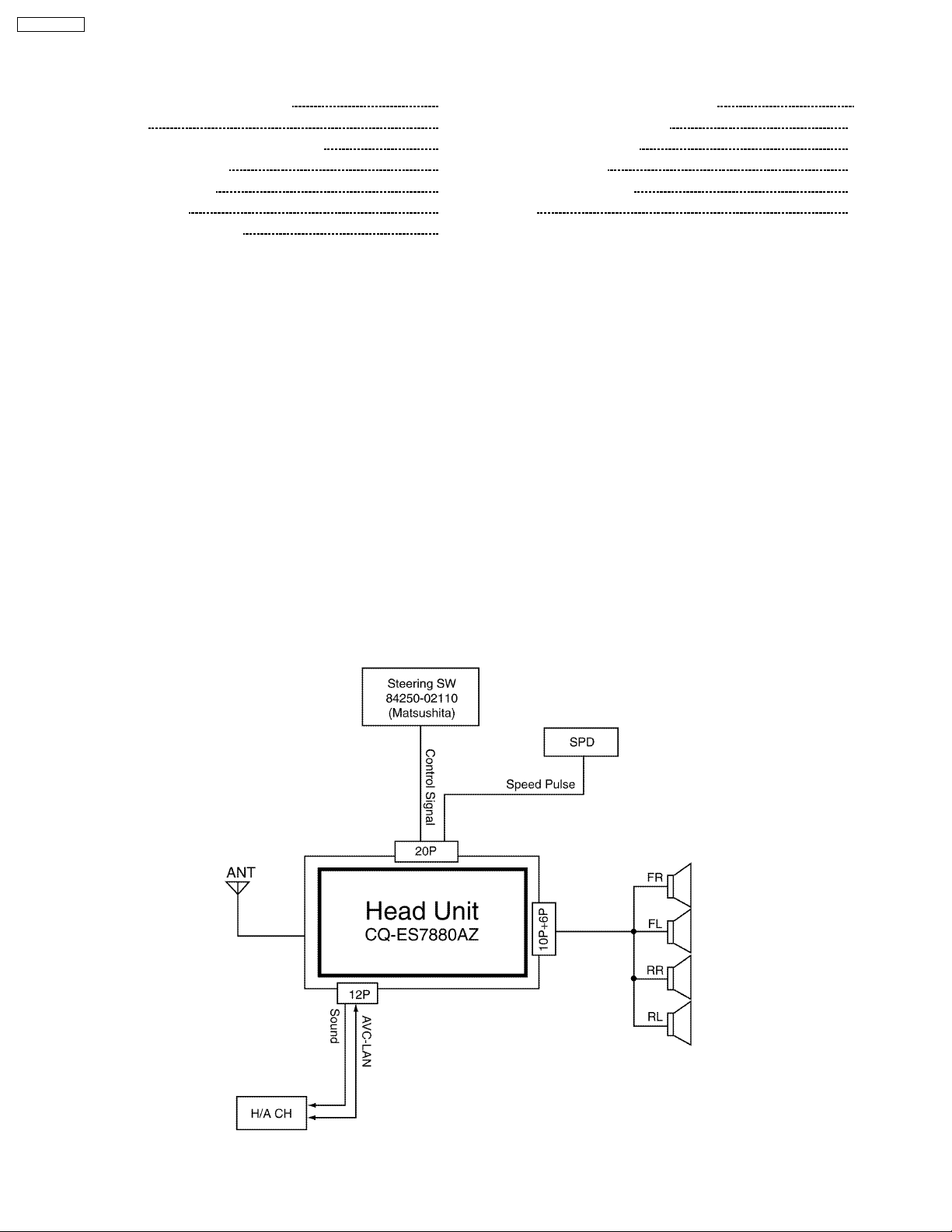
3 SYSTEM BLOCK DIAGRAM (For Testing)
*When this system is tested, this system diagram could be different from the actual vehicle.
2
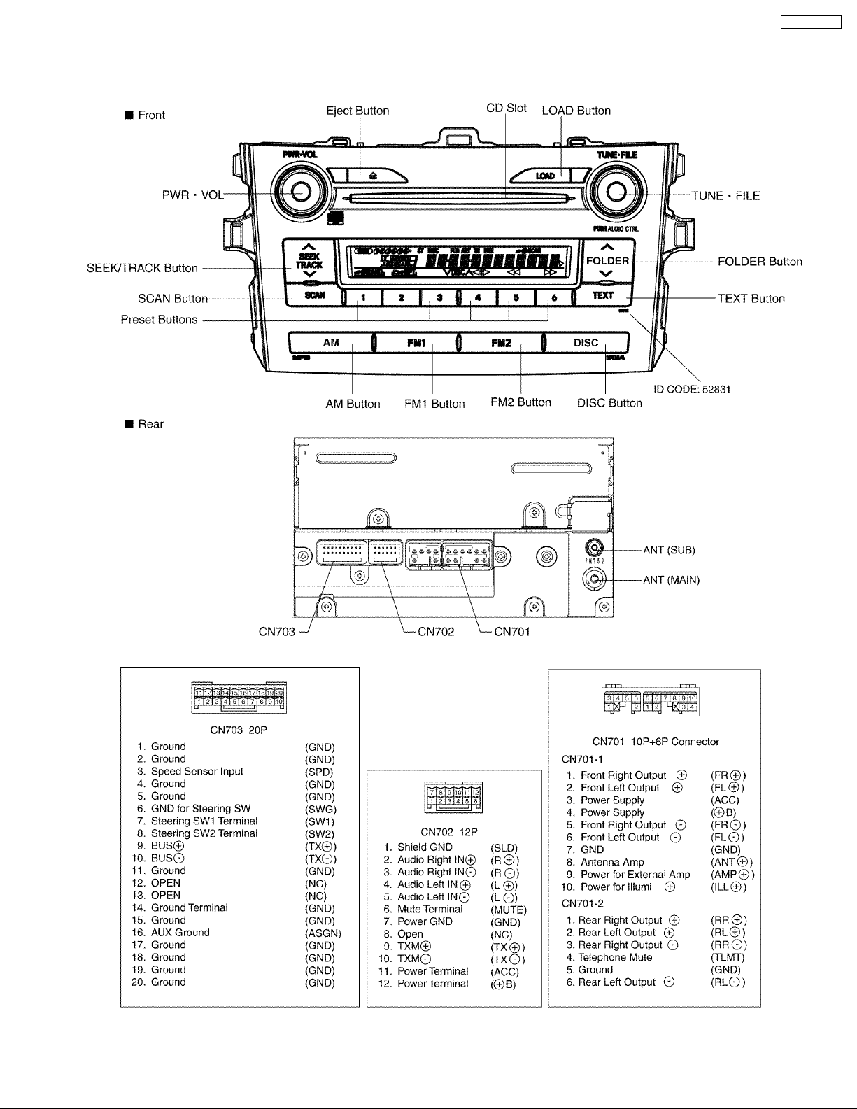
4 VIEWS AND FUNCTIONS
CQ-ES7880AZ
3
CQ-ES7880AZ
5 WIRING CONNECTION
4
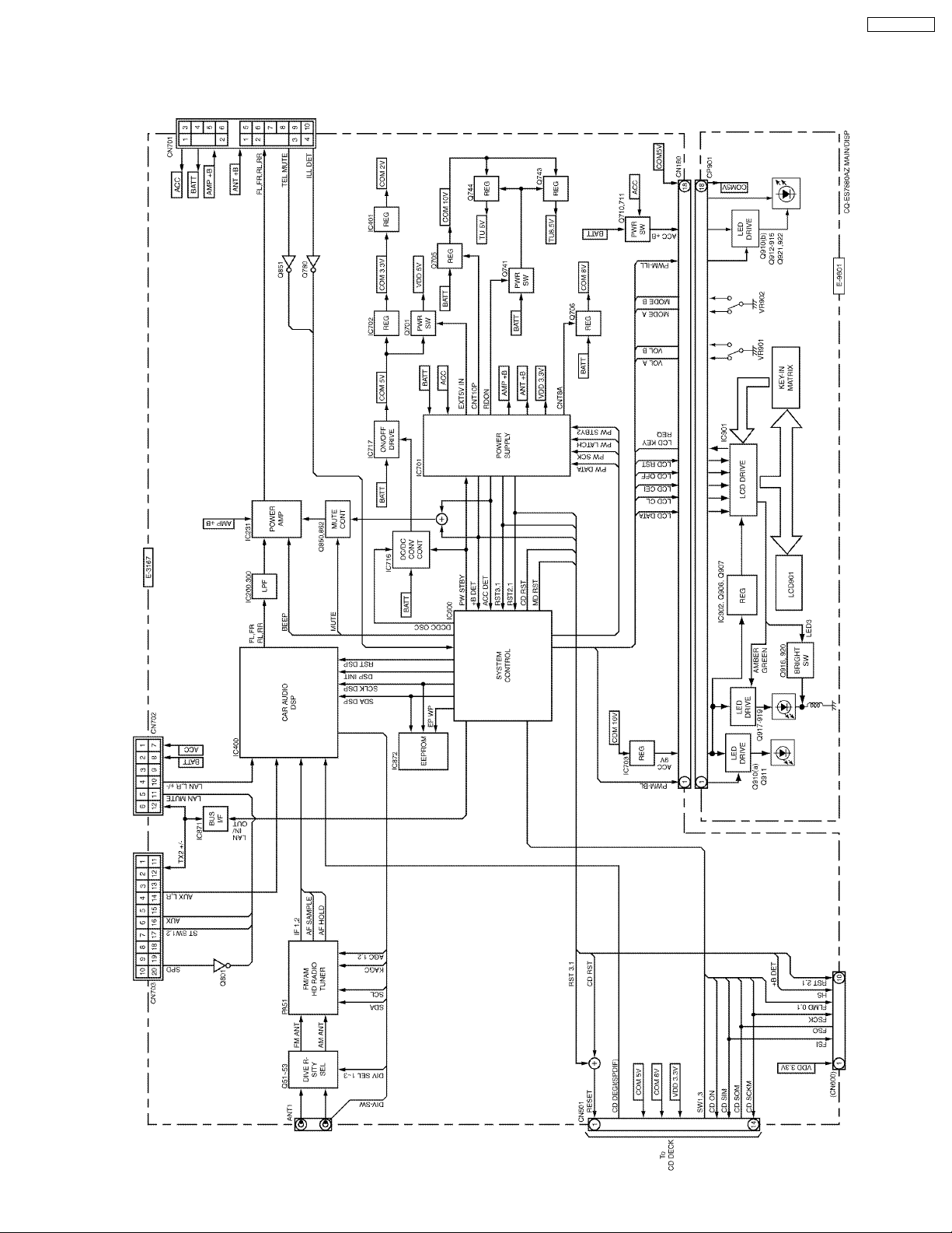
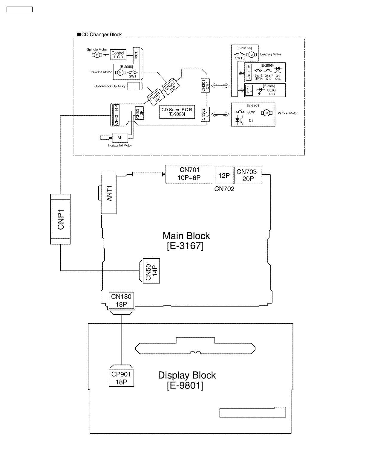
6 BLOCK DIAGRAM
6.1. Main / Display Block
CQ-ES7880AZ
5
CQ-ES7880AZ
7 TERMINALS DESCRIPTION
7.1. Main Block
IC600: C2DBYY000250
Pin
Port I/O Description FM
No.
1 AVDD - Standard voltage for A/D converter 3.5 3.5
2 GND - Ground Terminal 0 0
3 ILL-DET I H: Illumi off; L: Illumi on 3.5 3.5
4 LAN
MUTE
5 VDD - D/A converter standard voltage 3.5 3.5
6 MUTE O H: MUTE ON L: MUTE OFF 0 0
7 FAN - No connection - 8 IC/
FLMD0
9 VDD0 - Power Supply 3.5 3.5
10 REGCPU - Regulator output; stable-capacity
11 GND - Ground Terminal 0 0
12 X1 I Oscilllation terminal (main clock)
13 X2 O Oscilllation terminal (main clock)
14 RESET I H: Normal L: Reset 3.4 3.4
15 XT1 I Oscillation terminal (sub) 32.768kHz 0 0
16 XT2 - No connection - 17 SPEC
CHANGE
3
18 Lo-BAT I H: +B (3.1V or more)
19 SW1 - No connection - 20 DRST I On-chip debug terminal 0 0
21 NC - No connection - 22 CD-SOM I CD (IDC) deck serial communication 0 1.8
23 CD-SIM O CD (IDC) deck serial communication
24 CD-
SCKM
25 SPEC
CHANGE
1
26 NC - No connection - 27 SW3 - No connection - 28 BEEP O BEEP output terminal 0 0
29 SPD I Input terminal from the speed pulse;
30 SPEC
CHANGE
2
31 TX+ O AVC-LAN data input terminal 0 0
32 TX- I AVC-LAN data output terminal 0 0
33 GND - Input/output port and GND for the
34 VDD - Input/output port and power for the
35 NC - No connection - 36 NC - No connection - 37 LCD-ON
(PWM)
38 ILL-ON
(PWM)
39 DDI O On-chip Debug terminal 0 0
40 DDO O On-chip Debug terminal 0 0
41 DCK O On-chip Debug terminal 0 0
42 DMS O On-chip debug terminal 0 0
- - - -
- - 0 0
connection and power for when the
regulator stops
4.718MHz
4.718MHz
- - - -
L: +B (less than 3.1V)
H: data 1 L: data 0
O CD (IDC) deck serial communication
clock output terminal
- - - -
1pulse at 1/2548km
- - - -
combined functional terminal
combined functional terminal
O H: LCD backlight on L: LCD backlight off 3.8 3.8
O H: ILL ON L: ILL OFF 0 0
CD
AM
(V)
(V)
2.6 2.6
1.3 1.3
1.3 1.3
3.4 3.4
0 2.6
0 3.4
0 0
0 0
3.5 3.5
Pin
Port I/O Description FM
No.
43 DSP-
SDA
44 DSP-
SCL
45 WP I/O DSP (SAF7730HV) input/output (H/L) 3.2 3.2
46 PANEL
INFO
47 LCD-
RESET
48 NC - No connection - 49 LCD-CE1O - 0 0
50 LCD-
DATA
51 LCD-OFF O H: LCD on L: LCD off 5.2 5.2
52 LCD-CLK O LCD driver data clock output 5.2 5.2
53 NC - No connection - 54 NC - No connection - 55 NC - No connection - 56 DOLBY - No connection - 57 DC-DC
OSC
58 ACC-
DET
59 RESET
DSP
60 DSP-INIT I H: INIT completed; L: INIT incomplete 3.4 3.4
61 +B-DET I H: +B on L: +B off 3.5 3.5
62 RSE-
MUTE
63 L/R I H: Left handle L: Right handle 0 0
64 NC - No connection - 65 DIV-SW I H: Main is fixed L: Diver operation 3.2 3.2
66 TEL-
MUTE
67 CD-
RESET
68 CD-ON O H: CD deck CPU communication is
69 GND
(BVSS)
70 VDD
(BVDD)
71 NC - No connection - 72 NC - No connection - 73 LCD-
KEYREQ
74 NC - No connection - 75 NC - No connection - 76 FLMD1 I - 0 0
77 NC - No connection - 78 NC - No connection - 79 NC - No connection - 80 NC - No connection - 81 NC - No connection - 82 NC - No connection - 83 NC - No connection - 84 PW-
STBY2
85 PW-
STBY
86 PW-
LATCH
87 PW-SCK O Clock output for power IC (BD4902) 0 0
88 PW-
DATA
I/O DSP (SAF7730HV) input/output (H/L) 2.7 3.2
O DSP (SAF7730HV) input/output (H/L) 2.4 2.9
- - - -
O H: Normal; L: LCD when resetting 5.2 5.2
I/O LCD data input/output terminal 0 0
O Timer output 1.7 1.7
I H: ACC on; L: ACC off 3.5 3.5
O H: Normally DSP L: DSP RESET 3.5 3.5
- No connection - -
I H: VOL operation is valid
L: VOL operation is invalid
O H: Normal L: RESET 3.5 3.5
possible; L: Not possible
- Ground for bus interface 0 3.5
- Power supply for bus interface 3.5 3.5
I H: With key input data
L: No key data
O STBY2 output for power IC (BD4902) 3.5 3.5
O STBY output for power IC (BD4902) 3.5 3.5
O Latch signal output for power IC
(BD4902)
O Data output for power IC (BD4902) 0 0
CD
AM
(V)
(V)
3.5 3.5
0 3.5
0 0
3.5 3.5
6
Pin
Port I/O Description FM
No.
89 NC - No connection - 90 NC - No connection - 91 MODE-B I MODE encoder input terminal B 0 0
92 MODE-A I MODE encoder input terminal A 0 0
93 VOL-B I VOL encoder input terminal B 0 3.2
94 VOL-A I VOL encoder input terminal A 3.2 0
95 NC - No connection - 96 NC - No connection - 97 RE0-IN - No connection - 98 AUX I AUX detection terminal 3.2 3.2
99 ST-SW1 I KEY input 1 for steering SW input 3.2 3.2
100 ST-SW2 I KEY input 2 for steering SW input 3.2 3.2
AM
(V)
7.2. Display Block
IC901 : C0HBA0000205
Pin No. Port I/O Description V
1-3 LED1-3 O Led Output -
4 LED4 - No connection 5 Vss - Ground terminal 0
6 VLC5 - Power for LCD drive 0
7 VLC4 - Power for LCD drive 1.6
8 VLC3 - Power for LCD drive 3.1
9 VLC2 - Power for LCD drive 3.1
10 VLC1 - Power for LCD drive 4.5
11 VLCD - LCD drive voltage 6.1
12 VDD - Logic power supply 5.2
13 SYNC I/O Syncronized input/output
14 LCD OFF I LCD off input 5.2
15 RESET I Reset input 5.2
16 KEY REQ O Key request output 5.1
17 SCK I Shift clock input 5.1
18 DATA I/O Inputs commands , displayed
19 STB I Strobe input 1.1
20 OSC_IN I Oscillation terminal 2.7
21 OSC_OUT O Oscillation terminal 2.8
22-24 KEY1-3 I Key data input for key scan 1.6
25 KEY4 I Key data input for key scan 1.8
26-33 SEG1/KS1-
SEG8/KS8
34-85 SEG9-SEG60 O Segment output 3.1
86-89 SEG61/COM14-
SEG64/COM11
90-92 NC - No connection -
93-100 COM7-0 O Common output 3.2
terminal
datas, etc and outputs key
datas.
O Segment output and key
source output
O Segment and common output 3.1
CQ-ES7880AZ
CD
(V)
5.2
1.0
3.1
Note : Voltage measurements are with respect to ground, with
a voltmeter (internal resistance : 10M ohms).
7
CQ-ES7880AZ
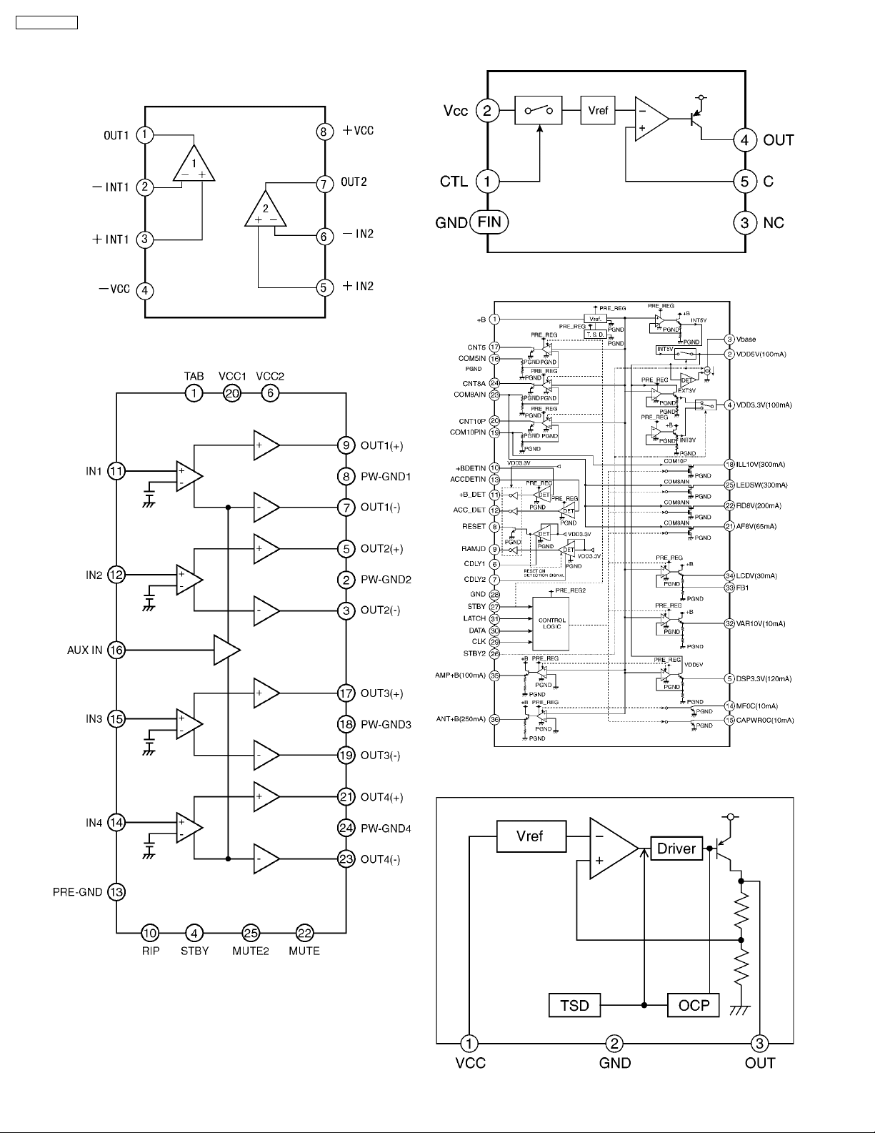
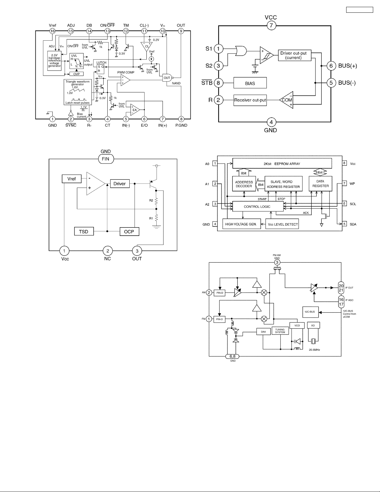
8 PACKAGE AND IC BLOCK DIAGRAM
8.1. Main Block
IC200, 300 : C0ABBB000220
IC401 : C0DBEJG00001
IC231 : C1BA00000447
IC701 : C1EB00000110
IC702 : C0CBABG00027
8
CQ-ES7880AZ
IC716 : C0DBAMC00006
IC703 : C0CBAHG00011
IC871 : C1BB00000844
IC872 : C3EBDC000070
PA51 : J3CCAZ000003
9
 Loading...