

Page 1

TOSHIBA
Service Training
PROJECTION
TELEVISIONS
Main Power Supply
NTDMOD05
& Complete
Shutdown Guide
TN50X81
TN55X71
TN55X81
TN61X81
TN40X81
TW56X81
TW65X81
Copyright 1999
TOSHIBA AMERICA CONSUMER PRODUCTS, INC.
NATIONAL SERVICE DIVISION
1420-B TOSHIBA DRIVE, LEBANON, TN 37087
Page 2

Contents
Overall Block Diagram.........5
Overall Block Diagram ..................................................................................... 6
Main Power Supply ..............7
Main Power Supply ........................................................................................... 8
VIN Terminal (pin 5) - Start Circuit ................................................................... 9
OCP/INH Terminal (pin 4) Function ................................................................. 9
Soft Start ........................................................................................................... 1 0
Surge Protect. .................................................................................................. 11
Oscillator/Constant Voltage Control Circuit ................................................ 12
Latch Block ...................................................................................................... 13
Overheat Protection Block (Internal to Q801)............................................. 13
Overvoltage Protection Block (Pin 5) ........................................................... 13
Latch Trigger Terminal (Pin 7)....................................................................... 1 3
Troubleshooting Flowchart ........................................................................... 14
Sub Power Supply..............1 5
Operation .......................................................................................................... 16
Start-up and Over Voltage Protect ................................................................ 17
Logic and Drivers............................................................................................ 18
Oscillator .......................................................................................................... 18
Oscillator Control ............................................................................................ 19
Latch ................................................................................................................. 19
Thermal Shock Detection Block ................................................................... 2 0
Over Current Protection................................................................................. 20
Soft Start ........................................................................................................... 2 0
Resonance Correction ................................................................................... 21
Additional Information .................................................................................... 22
Troubleshooting Flowcharts ......................................................................... 23
Shutdown ......................................................................................................... 25
Page 3

Basic Operation............................................................................................... 26
Monitoring Circuits ......................................................................................... 28
X-Ray Protection ............................................................................................. 28
+128V Over Current Protect .......................................................................... 29
+128V Over Voltage Protect ........................................................................... 3 0
Horizontal Stop Protection Circuit ................................................................ 31
+21V Over Voltage Protect ............................................................................. 32
+35V Over Current Protect ............................................................................ 3 3
+21V Over Current Protect ............................................................................ 3 4
-21V Over Current Protection ........................................................................ 35
+200V Low Voltage Protect ............................................................................ 36
Troubleshooting Flowchart ........................................................................... 37
Page 4

Page 5

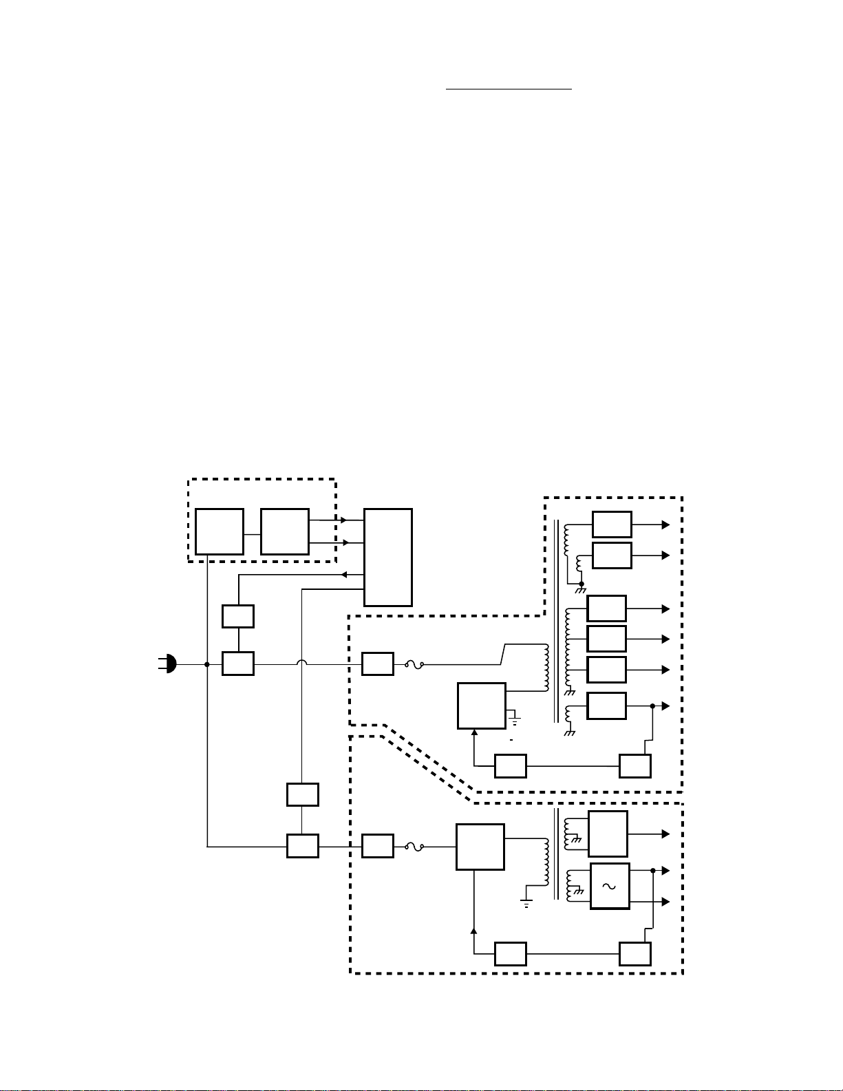
Overall Block Diagram
5
Page 6
Overall Block Diagram
Troubleshooting Tip:
Figure 1 is an overall block diagram of the standby ,
main, and sub power supplies in the progressive scan
televisions. The standby supply is always active
whenever the television is plugged into an AC line
source. It delivers 5V VDD and a reset 5V to the
microprocessor to keep it operational at all times,
even when the television is OFF . Transformer T840
isolates the standby supply from the live ground, and
D840 is a full-wave bridge rectifier that supplies 15V
DC to voltage regulator Q840 and relays SR81 and
SR83 (relay connections not shown). When the microprocessor receives an ON command from the remote control or power key on the front of the television, it sends 5V to the relay drivers to close relays
SR81 and SR83. Closing the relays supplies the AC
line input to the remaining two power supplies to operate the television.
Standby Supply
Standby
Regulator
Q840
5V=Relay On
0V=Relay Off
Q841
Relay
Q842
Drivers
5V=Relay On
0V=Relay Off
Relay
Drivers
Sub-Power Supply
Q844
Q843
SR83
Relay
+5-1
Microprocessor
5V
VDD
5V
Reset
QA01
Rectifier
D801
Main Switching IC
Rectifier
D861
AC Line
Input
Rectifier &
Isolation Trans.
D840
T840
SR81
Relay
F811
F860
If both relays never close, check the standby power
supply . Both the 5V VDD and the reset 5V are mandatory for the microprocessor to operate.
The main power supply and sub power supply work
independently from each other, so one supply can be
disabled to check the other. If the main power supply is disabled, the television would not have picture
or sound, but the microprocessor would still control
the relays. Therefore, the sub supply could be turned
ON and OFF and its voltages would appear as normal. If the sub power supply is disabled, everything
would work except the picture would be out of convergence. Either power supply can easily be disabled
by removing its fuse: F860 for the sub supply and
F811 for the main supply .
Main Power Supply
140V
Q801
Feedback
Main Switching IC
140V
Q888
Feedback
Photo
Coupler
QB03
Photo
Coupler
Q861
T861
18
19
21
20
D812
22
D810
12
3
D809
14
15
2
16
D808
17
Amp.
9
D887
17
3
2
T888
D888
10
13
12
14
Amp.
D811
D813
Error
&
D891
D895
Error
+7V
+7V
+35V
+15V
+11V
+128V
Q804
36.5V
21V
-21V
Q863
Figure 1. Overall Block Diagram
6
Page 7

Main Power Supply
7
Page 8

Main Power Supply
Photo
Coupler
+B
Error
Amp
O
S
C
T861
Q801
QB03
Q804
128V
140V dc
From D801
D808
The main power supply is a ringing choke converter.
Figure 2 is a block diagram for this supply . An oscillator (OSC) and a switching MOSFET are internal
to the main switching IC, Q801. During normal operation, D801 rectifies the AC line input to approximately 140V . This voltage is applied to the MOSFET
through transformer T861’s primary winding. As
shown in Figure 3a, when the MOSFET conducts,
current flows through T861’s primary windings and
builds an electromagnetic field. Figure 3b demonstrates that after the field builds, the MOSFET opens
to stop the current flow through T861. This causes
the electromagnetic field to collapse and induce current into the secondary windings.
Figure 2. Main Power Supply Block Diagram
When the MOSFET conducts,
current flows through T862,...
140V dc
From D801
Q801
O
S
C
When the MOSFET Stops conducting,
the electromagnetic field collapses...
T861
140V dc
From D801
Q801
T861
128V
D808
+B
O
...and an electromagnetic
field builds.
S
C
Error
Amp
Photo
Coupler
Q804
Coupler
QB03
Electromagnetic Field
Current Flow
(a) (b)
Figure 3. Main Power Supply Operation
+B
128V
D808
...and current is induced in
the secondary windings.
Error
Amp
Photo
Q804
QB03
8
Page 9

VIN Terminal (pin 5) - Start Circuit
0.5V
Drive Output
OCP/INH terminal
voltage
As shown in Figure 4, pin 5 (VIN) of Q801 is the
Startup and Over V oltage Protect (OVP) for Q801.
To start the operation of the power supply, 140V
draws current through resistors R802 and R803 which
builds a charge on capacitor C825. When the charge
reaches 22.5V, Q801 starts switching. Once Q801
is operating normally , the N
ode D805 provide 25V to pin 5 to maintain Q801’s
switching operation. At this time, C825 functions as
a filter capacitor.
Pin 5 is also the over voltage protection (OVP). If
the voltage on V
raises above 28V , an internal latch
IN
stops Q801 from operating. Refer to the Latch section for further details.
winding and rectifier di-
D
(2) INH Function (OFF Time Control)
At the same time the OCP comparator turns the
MOSFET OFF , the inhibit (INH) comparator stops
the oscillator and prevents the MOSFET and oscillator from operating until the OCP voltage drops
below 0.5V . The waveforms for this operation are
shown in Figure 6.
Q801
1
To T861
Drive
2
R803 & R802
From
D801
25V dc
D806
5 V
IN
D805
R825
C825
T861
N
D
Q801
OVP
Start
Figure 4. VIN T erminal and Start Circuit
OCP/INH Terminal (pin 4) Function
The OCP/INH terminal is a safety terminal that protects Q801 if an over current condition develops during
operation. Figure 5 shows this circuit diagram.
OCP
Latch
0.5V
INH
Oscillator
0.5V
Figure 5.
Over Current Protect (OCP)
and Inhibit (INH) T erminal
R807
4
R827
R828
(1) OCP Function (Over Current Protect)
When the MOSFET is turned ON, current flows
through resistors R827 and R828 and a voltage
develops at the over current protect (OCP) terminal at pin 4. If the voltage reaches 0.5V, the
internal OCP comparator turns the MOSFET
OFF and stops its current flow .
Figure 6.
OCP/INH W aveforms
9
Page 10

Soft Start
Without Soft Start
With Soft Start
The soft start circuit prolongs the life of the power
supply by reducing surge current at Turn on. Figure 7
shows the soft start circuit. When the power supply
starts up, a regulator inside Q801 outputs 3.1V on
the soft start terminal pin 7 that causes current flow
through the over current protect (OCP) resistors
(R827 and R828) and resistor R811. The additional
current flow makes the OCP more sensitive. The
increased sensitivity causes the OCP to trigger earlier
than normal which reduces current through the
MOSFET and T861’s primary windings. Once C818
is fully charged, current stops flowing through the OCP
resistors and normal operation begins. Figure 8 shows
the effect the soft start circuit has on the MOSFET’ s
drain current during startup.
Q801
1
To T861
Drive
2
R807
Over Current
Protect
4
C818
Latch Trigger
3.1V
Figure 7. Soft Start Figure 8. Soft Start Effect
R811
R827
7
R828
10
Page 11

Surge Protect.
Refer to figure 9. R815 and R816 reduce surge current through the main power supply at startup. They
provide additional resistance on the ground path of
rectifier D801. Relay SR85 and SR81 are disengaged before the supply operates. When relay SR81
closes, AC current is applied to rectifier D801. After
the supply begins to operate, it produces voltage
sources on the secondary of T861. T wo of the voltage outputs engage SR85. The 15V output supplies
a current source for SR85. The 7V source forward
biases Q805 to close the relay and provide a direct
ground path for D801 by bypassing R815 and R816.
Main Power Supply
Relay
SR81
R815
R816
Q801
D801
and
T861
SR85
Figure 9. Surge Protect
15V
7V
R832
R826
D823
Q805
11
Page 12

Oscillator/Constant Voltage Control
Circuit
Refer to Figure 10. Internal to Q801 is an oscillator
and oscillator control circuit. The oscillator controls
the switching MOSFET in Q801. To control the
power supply’s regulation, a feedback signal manipulates the oscillator frequency to maintain a consistent
current flow through the load.
Internal to Q801, Capacitors C2 and C3 and resistor R3 and R2 determine the MOSFET’ s base switching frequency . The MOSFET’s OFF time is a fixed
value determined by R3 in parallel with C3. C2 and
R2 determine the maximum duration of the
MOSFET’s ON time. An external pulse width modu-
lated (PWM) control signal, developed by any variance in the load current and coupled to the power
supply’s primary side by a photo-coupler , is applied
to the feedback (F/B) of Q801 on pin 6 to adjust the
charging time of C2 as required by the load. If the
load voltage decreases, the MOSFET’s ON time increases to compensate and increase the output of the
power supply . The longer the ON time, the larger the
electromagnetic field builds around T861’s primary
windings. The larger electromagnetic field induces
more current into the secondary windings when it
collapses. On the other hand, if the load voltage increases, the ON time decreases to reduce the overall
output of the power supply .
From Start Block
Regulator
Latch
R2
R3
Q801
Drive
Oscillator
C3
OCP
C2
To 25V VIN
F/B
6
R813
R814
128V Main B+
R817
R819
Q803
R818
Q804
Figure 10. V oltage Control
12
Page 13

Latch Block
Refer to Figure 11. A latch internal to Q801 stops
Q801’s operation to protect the IC from damage if a
problem occurs. Three conditions trigger the latch
circuit: Overvoltage on the V in (pin5), a temperature
above 1250 C on Q801’s frame, and a MOSFET’s
switching frequency that is too high. Once the latch
triggers, Q801 remains OFF until the AC power to
the circuit is removed. Q801’ s internal capacitor (C1)
is a delay that prevents the latch from engaging during
Startup.
nally to Q801, triggers the latch circuit when Q801’ s
frame temperature exceeds 125°C (minimum).
Overvoltage Protection Block (Pin 5)
Refer to Figure 11. The overvoltage protection circuit monitors the voltage on pin 5 (VIN) of Q801 and
engages the latch if the voltage rises above 28V . Refer to VIN T erminal section for further explanation.
Latch Trigger Terminal (Pin 7)
Overheat Protection Block (Internal to
Q801)
Refer to Figure 11. Because of the amount of current
flow through the MOSFET , the MOSFET generates
heat. The thermal shock detect (TSD), located inter-
5 VIN
Start-up & OVP
Soft Start
Trigger
Start
OVP
TSD
7
3.1V
9.9V
Regulator
Latch
R2
Refer to Figure 11. The Soft Start and T rigger (SS/
Tri) terminal (Pin 7) of Q801 monitors the switching
frequency of the internal MOSFET . If the frequency
increases excessively , C818 conducts and a voltage
develops on pin 7. If the voltage on pin 7 reaches
9.9V, the latch shuts Q801 OFF .
Q801
Drive
OCP
INH
Oscillator
0.5V
0.5V
Drain
Source
1
2
4
To T861
R807
R827
R828
R811
C818
C1
R3
3
C2
C3
Feedback
6
Figure 11. Internal Block Diagram of Q801
13
Page 14

Troubleshooting Flowchart
Caution:
Before removing or adding fuses,
remove all power from the
television and always use an Isolation
transformer when troubleshooting.
Start
Remove fuse F860.
Remove fuses F802,
F804, F808, F805, &
F806.
Connect a 100W
light bulb to F802’s
supply side.
Does relay
SR81 close when the
power button is
pushed?
Notes:
This flow chart is to help narrow the
cause of shutdown. Refer to the
circuit explanations for additional
information.
Disables the sub-power
supply.
Separates the loads from the
main supply
Substitutes the loads.
Without a load, the over
current protect triggers the
latch.
No
Yes
Replace Q801, Check
R827,R828, & the
feedback circuit.
Yes
Yes
Does +140V
appear at pin 1 of
Q801?
Are
pins 1 &2 of Q801
shorted to ground or
to each other?
Check the relay drive,
microprocessor and stand-by
power supply circuits.
No
Check R815, D801,C813 &
F811
No
Check D805, D806,
R827,R828, C881,
R803,& R802
14
Page 15

Sub Power Supply
15
Page 16

Operation
Photo
Coupler
Error
Amp
D
r
i
v
e
O
S
C
T888
C870
Q888
Q861
Q863
21V
140V from D861
-21V
The sub-power supply is a current resonance switching power supply . It supplies power to the digital
convergence and convergence boards. Figure 1 is a
block diagram for this supply . The primary winding
of T888 and capacitor C870 create an LC series
resonant circuit. An oscillator (OSC), drive circuit,
and two MOSFET s are located internal to switching
regulator Q888 (STR-Z4151). The OSC determines
the power supply’s switching frequency. The drive
circuit alternately switches the MOSFET s ON and
OFF . The two power MOSFET s, in a push-pull configuration, alternate the current flow through the LC
circuit during normal operation. The alternating current continually builds and collapses an electromagnetic field around T888’s primary windings. The col-
lapsing of the electromagnetic field induces current
into the secondary windings of T888. A full-wave
rectifier converts the induced current into a +21V line
and a –21V line.
T o regulate the secondary voltages, an error amplifier
monitors the +21V line and supplies a negative feedback to the oscillator through photo-coupler Q861.
Q861 isolates the primary side of the power supply
from the secondary . Refer to Figure 2. The power
supply’s switching frequency operates above the LC
resonant frequency . When the load on the secondary
side of the power supply increases and requires more
current, the oscillator frequency decreases and operates closer to the LC resonant frequency . The closer
the switching frequency is to resonance, the higher
the current flow through the primary windings of T888
and the larger the electromagnetic field. The larger
the electromagnetic field is when it collapses, the higher
the induced current is in the secondary winding. When
the load decreases and requires less current, the
switching frequency increases and moves away from
resonance. As a result, less current is induced in the
secondary windings.
Figure 1.
Sub-Power Supply
Block Diagram
Load
Current
Normal Operating Freqency is 70-80kHz
Increased
Load
Resonant Freq.
Operating Freq.
Decreased
Load
Switching
Figure 2.
Resonant Frequency
Freq.
16
Page 17

Start-up and Over Voltage Protect
Refer to Figure 3. A voltage divider (not shown)
uses the positive cycle of the line input to supply a
16V start-up pulse to pin 9 of Q888 via resistor R861.
After start-up, a drive circuit consisting of a secondary winding of T888, diode D864, and capacitor
C868 supply 16-20Vdc to pin 9 of Q888 to maintain
its operation. The voltage developed by the drive
circuit fluctuates with the switching frequency of the
power supply . Therefore, the voltage on pin 9 is also
applied to an over voltage protect (OVP) block internal to Q888. If the voltage on pin 9 increases to
22V , the OVP triggers the latch and switching stops.
Refer to the Latch section for further information.
D876 is a 27V zener diode that protects Q888 by
preventing excess voltage increases on pin 9.
From
D861
R861
16-20 Vdc
OVP
D876
9
Vcc
Q888
Start
Figure 3. Start-up
D864
C868
R871
T862
17
Page 18

Logic and Drivers
Oscillator
Refer to Figure 4. The logic block controls the
MOSFET s’ switching frequency. The outputs of the
logic block feed two drives that are powered by the
start block. After the start-up voltage is applied to
pin 9, the start block supplies a drive Vcc (DRI Vcc)
of approximately 8V to pin 10. Delaying the driver
supplies at start-up prevents damaging the MOSFET s.
The 8V on pin 10 powers driver B internally. To
power driver A, resistor R862 and diode D862 add
the voltage from pin 10 to the voltage on pin 15. D875,
C863, D873 and C873 are voltage regulators and
filters for these supplies.
D873
C873
R862 D862
D875
C863
IN
V
15
B+
130V
Out
14
COM.
12
To
T888
9
Start
Vcc
DRI Vcc
10 15
A
Logic
B
VB
Q888
Refer to Figure 5. Q888’s internal Oscillator devel-
ops the power supply’s switching frequency by gen-
erating a ramp waveform at capacitor terminal (CT)
pin 4. Capacitor C862, connected to pin 4, determines the lowest oscillation frequency. Both
MOSFET s are OFF for a short time when they are
alternately switching. This OFF time is called dead
time and is determined by resistor R867 on the dead
time (DT) terminal pin 3. Zener diode D872 is a
clamp.
Q888
OSC
3
R867
C862
4DT CT
D872
Figure 5. Oscillator
Figure 4. Logic and Drivers
18
Page 19

Oscillator Control
8
CD
TSD
OVP
Latch
Delay
OC/RC
C869
Q888
1 VIN
Latch
If the load current drawn from the 21Vdc line increases, the 21Vdc voltage begins to drop, decreasing the current through Q861’s LED side. The cur-
rent drop causes the LED to couple less light to the
photo transistor side and reduce the current flow into
pin 5 of Q888. This reduction in current flow varies
the OSC frequency , moving it closer to resonance to
increase the supply of current to maintain the 21Vdc
level. Conversely , if the load current decreases, the
21Vdc rises and increases the light through Q861 and
the current into pin 5 of Q888. The increased current
causes the OSC operating frequency to move away
from resonance to decrease the current supplied to
the load and level the 21Vdc.
21V
Load
OSC
Control
OSC
Refer to Figure 7. The latch block stops the operation of Q888 until the voltage on pin 1 of Q888 is
removed by turning the television OFF . Any of the
following detection blocks can trigger the latch.
• Over Voltage Protection (OVP) Block
• Thermal Shock Detection (TSD) Block
• Over Current Protection (OCP) Block
The charging time of capacitor C869, connected to
the capacitor delay (CD) terminal pin 8, delays the
operation of the latch circuit during start-up.
B
Q863
Out
G
B+
R883
Q861
R560
Q861
C
R895
C881
Figure 6. Oscillator Control
56Cont.
Q888
F
MAX
R868
Figure 7. Latch Block
19
Page 20

Thermal Shock Detection Block
The thermal shock detection block triggers the latch
if Q888’s internal temperature exceeds 150°C.
Over Current Protection
Refer to Figure 8. The over current detect (OC) senses
excess current in the LC series resonant circuit. As
current in the LC series resonant circuit increases, a
voltage develops at the over current protect (OC)
terminal pin 11. Resistor R870 and C874 detect the
current flow through the LC circuit. Resistor R866
samples the voltage and applies it to pin 11. Capacitor C867 is a filter to reduce ripple. Depending on
the input voltage, the over current protect responds
in one of two ways:
(1) OC Low Threshold V oltage: +1.8V
When the input voltage at the OC terminal is
higher than +1.8V, the voltage at the soft start (Css)
terminal pin 7 lowers and the soft start engages. By
reengaging the soft start, the main oscillator frequency
increases to reduce the current flow through the LC
circuit. The soft start continues to operate until the
voltage on pin 11 drops below 1.8V.
R872
OC
140V B+
11
C866
Q888
OC/RC
7
To
MOSFET (B)
Css
C867
OSC
Control
To pin 14,
Q888
R866
R870
OSC
T888
C874
C870
(2) OC High Threshold V oltage: +2.5V
If the input voltage at the OC terminal exceeds +2.5V , the oscillator frequency increases to its
maximum frequency and C866 discharges rapidly .
When the Css terminal voltage decreases to 0.7V,
the circuit resets and C866 charges again. The main
oscillator frequency decreases gradually . If this condition continues, the latch engages and oscillation
stops.
Soft Start
Refer to Figure 8. At start-up, the soft start is engaged by capacitor C866 on pin 7, soft start (Css)
terminal. While capacitor C866 charges, the switching frequency increases to reduce surge current through
the MOSFETs. Once C866 is fully charged, the
switching frequency goes to its normal operating frequency (approximately 70-80 kHz).
Figure 8. Over Current Protect
20
Page 21

Resonance Correction
Figure 9 shows the internal block diagram of Q888.
By monitoring MOSFET B’s gate, the over current
protect block (OCP) prevents the oscillator switching frequency from dropping below the LC resonant
frequency.
CD
From
C869
From
R866
Q888
TSD OVP Start
8
11
OC/RC
OC
Css Cont. F
From
C866
LatchDelay
Control
From
R864
To
R861
Vcc DRI Vcc
OSC
MAX
DT CT GND
Out
to VB
Ref.
OSC
From
R867
From
R862
From
R868
Logic
275634
From
DRI Vcc
15 VB109
A
B
1
IN
V
14
Out
12
COM.
Figure 9.
Internal Block Diagram of Q888
21
Page 22

Additional Information
Caution: Different input signals may cause a variance in voltage readings. The voltages and waveforms below
were recorded while displaying a color bar signal.
Pin 4, Q888
Dead Time
Internal Q888
Internal Q888
MOSFET (A)
Internal Q888
MOSFET (B)
Pin 14, Q888
C870
1.5 Vpp
On Off On
Off On Off
160Vpp
140 Vpp
Pin Name Vdc Description
1V
IN
140 Half bridge power input
2 GND 0 Control unit ground
3 DT 6 Dead time resistor terminal
4 CT 2.4 Oscillator capacitor terminal
5 CONT 5.9 Oscillator control terminal
6F
MAX
7 Css 3.7 Soft start capacitor terminal
6.2 Maximun frequency resistor terminal
8 CD 0.4 Delay latch capacitor terminal
9 VCC 18 Control unit power terminal
10 DRI 8 Gate drive power output
11 OC 0.7 Out of resonance / over current detection
12 COM 0 Half bridge GND
14 OUT 71 Half bridge output
15 VB 78 High side gate drive power input
22
Page 23

Troubleshooting Flowcharts
Caution:
Before removing or adding fuses,
remove all power from the
television and always use an Isolation
transformer when troubleshooting.
Using the isolated
ground, check the
voltage on the power
supply side of fuse
F863.
Start
Remove fuse F811.
Remove fuses F861,
F863 and F864.
Does relay
SR83 close when the
power button is
pushed?
Yes
Does the
No Yes
power supply make
a soft "tick-tick"
sound?
Disables main power supply
Disconnects the loads
on secondary side
No
Check the relay drive,
microprocessor and stand-by
power supply circuits.
Check Drive Circuit:
D864,R871 and C868.
Yes
Connect a 100W
light bulb to F470’s
supply side.
No
Check: Feedback Circuit: Q862,Z801
Resonate Capacitor: C870
Over Current Protect: R865,R870
Soft Start: C866
Does a
constant voltage
appear at F863’s
supply side?
Does the
voltage regulate
at 21Vdc?
23
No
Turn to next page.
Yes
The power supply is
operating normally.
Page 24

Caution:
Before removing or adding fuses,
remove all power from the
television and always use an Isolation
transformer when troubleshooting.
Voltage appears then drops.
Continued from the
previous page.
With fuse F863 still open,
check the voltage on the power
supply side of F863 when the
television is first turned on.
Does the
voltage at F863 rise
to >21V then drop, or does
the voltage never
appear?
Voltage never appears.
Check: Feedback: Q861,Q863,
D881
Voltage is present.
Check: Oscillator Terminal: C862, D872
DRI Circuit: D862, R862, D875
Start-up:R861,D876
Latch Delay Capacitor: C869
Using the
live ground, check
for 140V on pin 1
of IC888.
Check: Fuse F8860. If open, replace Q888.
No voltage.
Rectifier: D861
Filter Capacitor: C857
24
Page 25

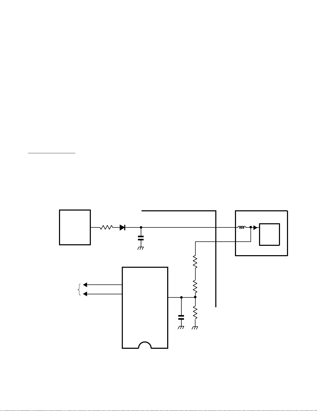
Shutdown
25
Page 26

Basic Operation
The shutdown circuit is a safety device that bypasses
the microprocessor to turn OFF the relays (SR81
and SR83 not shown) if certain problems occur in the
television. As shown in Figure 1, the protect circuit’s
main component is the silicon controlled rectifier D846
(SCR). The SCR has an anode and a cathode like a
diode and a gate that acts like an ON switch. When
0.825V appears on D846’s gate, current flows
through its anode-cathode junction in the same direction as a standard diode. Removing the voltage from
D846’s gate does not stop the anode-cathode current flow . Once the anode and cathode conduct, they
continue to conduct even after the gate voltage is removed. Removing the current flow between the anode-cathode resets the SCR.
T en monitoring circuits in the television can send the
necessary voltage to the SCR’s gate to start the SCR’s
anode-cathode current flow . When the SCR conducts, transistor Q845 turns ON and its collector
voltage drops close to ground. Q845’s collector ap-
plies this potential to the relay drivers to turn them
OFF and disengage the relays. The microprocessor
senses that the relay drivers are OFF and blinks the
power LED every half-second to indicate a shutdown
condition. Unplugging the television resets the SCR.
Troubleshooting tip:
Because of the speed of the shutdown circuit, technicians may have difficulties getting proper voltage readings when this circuit activates. A peak-response or
min/max meter is necessary for troubleshooting a shutdown problem. These meters can read a voltage in a
split second and store the reading into memory for
easy recovery . If a peak-response meter is not available, try using an oscilloscope on the dc setting. The
scope reacts quicker that the digital voltmeter, and
the change in dc level can be seen on the scope’s
CR T . However, most scopes do not have a dc voltage readout or the ability to record the value. The
lack of these features makes getting an accurate dc
voltage reading difficult. Therefore, the peak-response meter is the preferred method for measurement.
Caution:
Always use an isolation transformer when troubleshooting televisions.
26
Page 27

+35V OCP
R370
Q370
D371
D819
D818
+128V OVP
+21V OCP
R7750
Q759
R7756
Q762
D490
D7701
D820
R4039
Q492
+128V OCP
+15V OVPD817-21V OCP
D891
+21V OVP D892 H. Stop 1
D439
From +5V
D846
SCR
Cathode
Anode
Gate
D473
R847
D454
Q452
D438
Q432
Q429
Q430
H. Stop 2
X-Ray
Main Supply
Relay Drivers for SR81
Sub-Power Supply
Relay Drivers SR83
D850
D845
Q845
Figure 1.
Overall Block Diagram
R846
R845
5V Relays ON
0V Relays OFF
= Shutdown
0.7 V
Microprocessor
0 V = Normal
OVP = Over Voltage Protect
OCP = Over Current Protect
QA02
27
Page 28

Monitoring Circuits
X-Ray Protection
T o help find the cause of a shutdown condition, it is
necessary to know the operation of each monitoring
circuit and the conditions that trigger shutdown. The
following circuit explanations describe the operation
of each monitoring circuit, give a test point for each
circuit, and provide troubleshooting tips to help in the
repair of the TV . Use the troubleshooting flowchart
at the end of this section to help determine which
monitoring circuit is causing shutdown. Please take
note: the troubleshooting tips and flowcharts in the
following sections are intended as a troubleshooting
guide, NOT an answer to all situations.
Warning!!
T oshiba does not recommend disconnecting the shutdown circuit for troubleshooting. Disconnecting the
shutdown circuit increases the possibility of a failure
damaging the television.
Figure 2 demonstrates the x-ray protection monitoring circuit that triggers shutdown if it detects excessive x-ray radiation, which is produced by an increase
in high voltage. T461’s secondary winding across
pin 9, diode D471, and capacitor C471 produce a
DC voltage directly proportional to the high voltage
(HV). A resistor divider consisting of resistors R451,
R452, and R453 reduces the voltage and applies it to
the emitter of Q430. As the high voltage increases,
the voltages at C471 and on the emitter of Q430 increase proportionately . Connected to Q430’s base
is zener diode D472. If the voltage on the emitter is
large enough, D472 conducts and turns Q430 ON.
Q430’s conduction increases the voltage on its col-
lector to turn Q429 ON. When Q429 turns ON,
current flows between its emitter and collector, and a
voltage appears on its emitter . This voltage is applied
to SCR D846. The SCR turns ON and shuts the
television down. Use D473’s anode as the test point
for troubleshooting.
T461
R448
C471
R452
R450
R453
D471 R451
9
Figure 2. X-Ray Protection
6V
12V
Q430
0V Normal
>
2.5 V Shutdown
Q429
0V
R454
6.1V
D472
D473
To
SCR’s
Gate
Troubleshooting Tips:
Problems with the horizontal outputs, resonance ca-
pacitors, flyback transformer, deflection yokes, or a
shorted CRT may trigger shutdown. Refer to the service manual for part numbers, part values, and schematic diagrams.
• The CR Ts are the most likely culprit of an x-ray
protection shutdown. Each CR T can be disconnected separately by disconnecting the drive PC
board. The television can operate with one of
the CRT s disconnected without damaging the remaining CR T s or television. A CRT may intermittently arc and cause intermittent shutdown.
LIGHTL Y tapping on the neck of the CR T may
duplicate this symptom. T ake caution when tapping. T apping too hard can damage the CR T’s
neck.
• A shorted secondary winding of the flyback
transformer or distributor block can increase the
high voltage. A ringing check may indicate a bad
flyback transformer; however, replacement of the
flyback transformer or distributor block may be
necessary to determine unequivocally if they are
defective.
28
Page 29

+128V Over Current Protect
0V Normal
2.5 V Shutdown
>
Load
Q492
R4040
R4039
R4041
To Gate
of D846
D491 D490
R4038
C497
Main Power
Supply
128V
R4042
C498
As shown in Figure 3, resistor R4039 is the over current protect (OCP) sensing resistor that monitors the
current flow through the +128V line. During normal
operation, Q492 is turned OFF and its collector voltage is 0V. An increase in current through the load
increases the voltage drop across R4039. If the current increases enough, the voltage across R4039 forward-biases Q492 and turns it ON. When Q492
turns ON, its collector voltage increases towards the
supply voltage. T o trigger shutdown, resistor R4043
supplies the collector voltage to D846’s gate through
zener diode D491 and diode D490. Use D491’s an-
ode as the test point for troubleshooting.
Capacitor C498 provides a delay that prevents surge
current from triggering the shutdown when the television is first activated.
Troubleshooting Tips:
Either a shorted horizontal output, high voltage out-
put, flyback transformer, or the horizontal output’s
resonance capacitors can pull excessive current
through R4039 and cause the +128V OCP to trigger
shutdown. Other possibilities are: improper power
supply regulation or R4039 is increasing in value.
• T o check the main power supply, refer to the Main
• A shorted horizontal output or high voltage out-
• Lastly , the over current sensing resistor R4039
Power Supply troubleshooting chart within the
Main Power Supply section of this module.
put transistor (Q404 and Q416 not shown) is the
most likely culprit of this problem. However, a
shorted flyback transformer, arcing in a CR T , or
a shorted yoke may have caused one of the outputs to short. A ringing test can indicate a short
in a yoke or a flyback’s winding. Nevertheless,
replacement of the yoke and transformer might
be necessary to determine the failed part. For
tips on troubleshooting the CR T , resonance capacitors, and anode caps, refer to the x-ray protect circuit in the previous paragraphs.
can slightly increase in value and cause a false
shutdown intermittently or at Turn on when the
high voltage first develops.
Figure 3. +128V Over Current Protect
29
Page 30

+128V Over Voltage Protect
The +128V over voltage protect (OVP), shown in
Figure 4, monitors the +128V supply and triggers
shutdown if the voltage increases excessively . If the
supply voltage rises above D818’s zener voltage, the
diode conducts and delivers a logic HIGH (approximately 2.5V or higher) to the anode of diode D819
which applies the voltage to D846’s gate to trigger
shutdown. Normal voltage at the anode of D819 is
about 0V. A voltage of 2.5V or GREA TER at this
point results in shutdown. Use a peak-hold meter at
this point for troubleshooting.
Troubleshooting tip
One way a supply voltage increases is by a loss of
load. However, with this supply , a loss of load will
not increase the supply voltage enough to trigger the
OVP . If the OVP is triggering shutdown, the main
power supply is producing excessive voltage. Usually , a loss of feedback in the power supply circuit
causes an increase in the supply’s output voltage.
Refer to the Power Supply Section of this module for
more information on the main power supply .
>
D818
(30V)
R822, R830,
&R831
Solder Link
R824
D808
T861
R820
C832
Figure 4. +128 Over Voltage Protect
0V Normal
2.5 V Shutdown
D819
To Gate
of D846.
+128V
Load
30
Page 31

Horizontal Stop Protection Circuit
Because the horizontal deflection and the high voltage circuits operate separately , the high voltage circuit can still produce an output if the deflection circuit
fails. If this scenario happens, one bright vertical line
would appear on the screen and burn the phosphors
of all three CRTs. However, to prevent the vertical
line from damaging the CRTs, two horizontal stop
protection circuits engage the shutdown circuit and
blank the picture if a loss of deflection occurs. Refer
to Figure 5 for the following explanation of the first
horizontal stop circuit. T462 is the horizontal deflection transformer. During normal operation, current is
induced into the secondary windings between pins 3
and 1. Diode D451 rectifies the current, and capacitor C466 filters it to produce a DC voltage that resistor R490 applies to the base of transistor Q451.
Q451’s emitter connects to the base of Q452. Dur-
ing normal operation, both of these transistors are ON,
making Q452’s collector voltage approximately 3.6V .
If horizontal deflection is lost, the voltage applied to
the base of Q451 drops and both transistors turn OFF .
The voltage on the collector of Q452 increases to
10.8V, and diodes D454 and D439 apply the voltage to the gate of SCR D846 to shut down the television. Q452 also applies the collector voltage to the
blanking circuit to black out the picture and protect
the CRT s .
Figure 6 shows the second horizontal stop circuit that
works in the same manner as the first horizontal stop
circuit. Transistor Q441, capacitor C450 and diode
D440 prevent the shutdown circuit from engaging
when the television is first turned ON. At Turn on,
the 12V appears before the horizontal deflection is
fully operational. During this time, Q452 is OFF and
10.8V appears on its collector to engage the blanking circuit. Normally this voltage would also engage
the shutdown. But when the power is first applied,
capacitor C450 charges and allows current to flow
through Q441’s base – emitter junction to turn it ON.
While Q441 is ON, its collector voltage is at ground
which prevents the 10.8V application to the SCR.
Once C450 reaches its full charge, Q441 turns OFF .
By this time, horizontal deflection has started and the
circuit is operating normally .
Troubleshooting tip:
The television uses two horizontal stop circuits to pre-
vent damage if T462 shorts. If one of the horizontal
stop circuits is causing shutdown, check T462 for
shorted windings.
R419
3
T462
1
D451
C446
9.3V
R490
8.7V
R493
12V
Q451
3.6V
Q452
4.2V
R494
3.6V
D453
Figure 5.
First Horizontal Stop Protect
R495R496
C450
D440
To Blanking Circuit
(7.5V)
D454
(7.5V)
From
H. Stop 2
Q411
D452D456
0V Normal
>
2.5 V Shutdown
D439
To D846
Gate
31
Page 32

12V
To Blanking Circuit
R431
6
T462
5
D431
C415
9.1V
R432
8.4V
R434
+21V Over Voltage Protect
Q431
R436
Q432
3.6V
R435
4.2V
R437
D433
3.6V
C450
D440
Figure 6.
Second Horizontal Stop Protect
(7.5V)
D438
(7.5V)
From
H. Stop 1
Q411
D432D436
0V Normal
>
2.5 V Shutdown
D439
To D846
Gate
The +21V over voltage protect (OVP) monitors the
+21V output of the sub-power supply and triggers
shutdown if the voltage increases excessively . Refer
to Figure 7. If the +21V supply voltage rises enough
to break D892’s zener voltage, the diode conducts
and delivers a logic HIGH (approximately 2.5V or
higher) to the anode of diode D891. D891 applies
the voltage to D846’s gate to trigger shutdown. Nor-
mal voltage at the anode of D891 is about 0V. A
voltage of 2.5V or GREA TER at this point results in
shutdown. Use a peak-hold meter at this point for
troubleshooting.
Troubleshooting tip
A supply voltage increases when there is a loss of
load. However with this supply , a loss of load will
not increase the supply voltage enough to trigger the
OVP. If the OVP is triggering shutdown, the sub
power supply is producing excessive voltage. Usually , a loss of feedback in the power supply circuit
causes an increase in the supply’s output voltage.
Refer to the Sub Power Supply Section of this module for more information on the sub power supply .
T861 D897
D898
Figure 7. +21 Over Voltage Protect
D892
(22V)
+21V
Solder Link
0V Normal
>
2.5V Shutdown
R893
D891
To Gate
of D846.
Load
32
Page 33

+35V Over Current Protect
The +35V over current protect (OVP) monitors the
current through the +35V line. This supply is developed by the main power supply and supplies the vertical output Q301 and other transistor switching circuits. As shown in Figure 8, current flows through
the current sensing resistor R370. If the load current
becomes excessive, the voltage drop across R370
increases and turns ON transistor Q370. When Q370
turns ON, the collector voltage increases towards the
+35V supply and Zener diode D370 conducts to
deliver a voltage to the gate of SCR D846. Use the
peak-response meter on D371’s anode for a test
reading.
Troubleshooting Tips:
A shorted vertical output Q301 is the likely cause of
excessive current draw from the +35V line. If the
vertical output fails, usually pins 1 and 2 or 1 and 6
short together.
+35V
Main Power
Supply
Q370
R370
R372
R371
0V Normal
>
2.5 V Shutdown
R373
D370 D371
Figure 8. +35V Over Current Protection
Load
To D846
Gate
33
Page 34

+21V Over Current Protect
Figure 9 is the circuit diagram for the +21V over
current protect (OCP). Resistor R7750 is the over
current sensing resistor that monitors the current flow
to the convergence outputs (Q751 and Q752 not
shown). An increase in current increases the voltage
drop across R7750. During normal operation,
transistors Q759 and Q758 are turned OFF and
transistor Q757 is ON. Because Q757 is turned ON,
the voltage at its collector is 0V . A slight increase in
the voltage across R7750 turns ON Q759 and
increases its collector voltage. Then Q758 turns ON,
and its collector voltage drops to ground and turns
OFF Q757. The emitter-collector current of Q757
stops and the voltage on the collector rises to a logic
HIGH (approximately 2.1V or higher). The logic
HIGH is applied to the gate of the SCR D846 through
D7701, and shutdown takes place. Because transistor
Q757 is also controlled by the -21V over current
protect, the collector of Q759 should be used as the
test point. A voltage of 0.8V or GREA TER at this
point indicates the transistor is turning ON and
activating shutdown.
Transistor Q783 is always slightly forward biased to
reduce the sensitivity of the shutdown circuit and
prevent false shutdowns.
Troubleshooting Tips:
• The over current sensing resistor can increase in
value and cause a false or intermittent shutdown.
Make certain the current sensing resistor is the
proper value.
• If excess current is pulled from the power supply ,
check the convergence output ICs (Q752 and
Q751 located on the convergence output PC
board) and the surrounding biasing resistors. The
digital convergence board can cause Q752 and
Q751 to work too hard and pull excess current.
If this is suspected, remove the digital
convergence board from the television with the
television unplugged. Plug the television back in
and turn it ON if necessary . If the television comes
ON*, the digital convergence board may be bad.
If the television still shuts down, Q752, Q751, or
their surrounding biasing circuits may be bad.
* The television can power up without the digital convergence board in place, but the television will be out
of convergence. The raster bows in from all sides
because the horizontal and vertical scans are not going all the way to the edge of the CR T s. Do not let
the television run for an extended time in this condition. If left in this condition long enough, it can burn
the phosphorous. If additional testing is required in
this condition, turn the contrast and brightness all the
way down to reduce the risk.
R7703
R7704
Sub-Power
Supply
Q783
1.2V
R7702
+21V
R7701
7.7V
Q759
0.6V
0V Normal
>
0.8 V Shutdown
R7750
C7760
R7745
R7747
Q758
R7749R7751
-21V OCP
From
Q757
34
Load
Stand by
+5V
R7742
D7701
To D846's
Gate
Figure 9. +21 Over Current Protect
Page 35

-21V Over Current Protection
The –21V OCP operates in the same manner as the
+21V OCP . Refer to Figure 10 and the explanation
for the +21V OCP for details.
R7752
R7753
Sub-Power
Supply
Q784
R7706
Figure 10. – 21V Over Current Protect
-21V
R7763
R7705
C7763
Q762
0V Normal
>
-0.8 V Shutdown
R7765
R7745
R7758
Q761
11
Load
R7764
Stand by
+5V
R7742
D7701
Q757
To D846's
Gate
From
+21V OCP
35
Page 36
+200V Low Voltage Protect
Refer to figure 11. Pins 3 and 5 of the flyback
transformer provide the source for the 210V to the
CR T drive circuit. D406 and C496 rectify the 210V .
A loss of this voltage results in excessive cathode
current in the CR T. This excess current would damage
the CR T by burning the phosphors.
The 200V low voltage protection circuit turns the
television off if a loss of the 210 volts occurs. Internal
to Q302 is a reference voltage of 6.25 volts. If the
voltage on pin 10 drops to the 6.25 volt reference,
Q302 communicates through the I2C bus to the
microprocessor . The microprocessor then turns off
the television and blinks the power indicator.
Troubleshooting Tip:
Unlike the shutdown mode, the television can be
turned back on by the power button on the remote.
The television does not have to be unplugged first.
Flyback
Trans.
To
Microprocessor
2
C BUS
I
Deflection Board
P405
3
D406
210V
158
+
C496
159
CRT Drive Board
1
Video
2
Drive
R417
14
15
16
R418
R327
Q301
TA1241
Figure 11. 200 V Low Voltage Protect
36
Page 37

Troubleshooting Flowchart
Caution:
Before removing or adding fuses,
remove all power from the
television and always use an Isolation
transformer when troubleshooting.
Yes
Remove fuse F804.
Start
Remove fuses
F863 & F864.
Apply power
to the TV. Does it still
shut down?
Notes:
This flow chart is to help narrow the
cause of shutdown. Refer to the
circuit explanations for additional
information.
With F804 open, the television
may power up but not have a
picture. This does not mean the
television is still in shutdown.
Shutdown is indicated
by the relays disengaging
after closing, and that the power cord
must be unplugged and plugged back
in for the relays to reengage.
Key:
OVP = Over Voltage Protect
OCP = Over Current Protect
No
Check the
+21V OCP & -21V OCP
Yes No
With F804 still out of circuit,
remove fuse F806.
Yes
Check the
125V OVP, 125V OCP
+21V OCP
Apply power
to the TV. Does it still
shut down?
Apply power
to the TV. Does it still
shut down?
Check the
H. Stop 1, H. Stop 2,
+15 OVP, & X-Ray protect
No
Check the
+35V OCP
37
Page 38

38
 Loading...