

TOSHIBA Original CMOS 32-Bit Microcontroller
TLCS-900/H1 Series
TMP92CH21FG
Semiconductor Company

Preface
Thank you very much for making use of Toshiba microcomputer LSIs.
Before use this LSI, refer the section, “Points of Note and Restrictions”.

CMOS 32-bit Microcontroller
TMP92CH21FG/JTMP92CH21
1. Outline and Device Characteristics
The TMP92CH21 is a high-speed advanced 32-bit Microcontroller developed for controlling
equipment which processes mass data.
The TMP92CH21 has a high-performance CPU (900/H1 CPU) and various built-in I/Os.
The TMP92CH21FG is housed in a 144-pin flat package. The JTMP92CH21 is a chip form
product.
Device characteristics are as follows:
(1) CPU: 32-bit CPU (900/H1 CPU)
• Compatible with TLCS-900/L1 instruction code
• 16 Mbytes of linear address space
• General-purpose register and register banks
TMP92CH21
• Micro DMA: 8 channels (250 ns/4 bytes at f
(2) Minimum instruction execution time: 50 ns (at f
= 20 MHz, best case)
SYS
= 20 MHz)
SYS
(3) Internal memory
• Internal RAM: 16 Kbytes (can be used for program, data and display memory)
• Internal ROM: 8 Kbytes (used as boot program)
Possible downloading of user program through either USB,
UART or NAND flash.
(4) External memory expansion
• Expandable up to 512 Mbytes (shared program/data area)
• Can simultaneously support 8,- 16- or 32-bit width external data bus
... dynamic data bus sizing
• Separate bus system
(5) Memory controller
• Chip select output: 4 channels
(6) 8-bit timers: 4 channels
(7) 16-bit timer/event counter: 1 channel
(8) General-purpose serial interface: 2 channels
• UART/synchronous mode: 2 channels (channel 0 and 1)
• IrDA ver.1.0 (115 kbps) mode selectable: 1 channel (channel 0)
92CH21-1
2009-06-19

(9) USB (universal serial bus) controller: 1 channel
• Compliant with USB ver.1.1
• Full-speed (12 Mbps) (Low-speed is not supported.)
• Endpoints spec
Endpoint 0: Control 64 bytes* 1-FIFO
Endpoint 1: BULK (out) 64 bytes* 2-FIFO
Endpoint 2: BULK (in) 64 bytes* 2-FIFO
Endpoint 3: Interrupt (in) 8 bytes* 1-FIFO
• Descriptor RAM: 384 bytes
2
S (Inter-IC sound) interface: 1 channel
(10) I
2
S bus mode/SIO mode selectable (Master, transmission only)
• I
• 32-byte FIFO buffer
(11) LCD controller
• Supports up to 4096 color for TFT, 256 color, 16, 8, 4 gray levels and B/W for STN
• Shift register/built-in RAM LCD driver
TMP92CH21
(12) SDRAM controller: 1 channel
• Supports 16 M, 64 M, 128 M, 256 M, and up to 512-Mbit SDR (Single Data Rate)-SDRAM
• Possible to execute instruction on SDRAM
(13) Timer for real-time clock (RTC)
(14) Key-on wakeup (Interrupt key input)
(15) 10-bit AD converter: 4 channels
(16) Touch screen interface
• Available to reduce external components
(17) Watchdog timer
(18) Melody/alarm generator
• Melody: Output of clock 4 to 5461 Hz
• Alarm: Output of 8 kinds of alarm pattern and 5 kinds of interval interrupt
(19) MMU
• Expandable up to 512 Mbytes (3 local area/8 bank method)
• Independent bank for each program, read data, write data and LCD display data
(20) Interrupts: 50 interrupt
• 9 CPU interrupts: Software interrupt instruction and illegal instruction
• 34 internal interrupts: Seven selectable priority levels
• 7 external interrupts: Seven selectable priority levels (6-edge selectable)
(21) Input/output ports: 82 pins (Except Data bus (16bit), Address bus (24bit) and
(22) NAND flash interface: 2 channels
• Direct NAND flash connection capability
• ECC calculation (for SLC- type)
92CH21-2
RD pin)
2009-06-19

TMP92CH21
(23) Stand-by function
• Three HALT modes: IDLE2 (programmable), IDLE1, STOP
• Each pin status programmable for stand-by mode
(24) Triple-clock controller
• Clock doubler (PLL) supplies 48 MHz for USB, 36 MHz system-clock for others
• Clock gear function: Select high-frequency clock fc to fc/16
• RTC (fs = 32.768 kHz)
(25) Operating voltage:
• VCC = 3.0 V to 3.6 V (fc max = 40 MHz)
• VCC = 2.7 V to 3.6 V (fc max = 27 MHz)
(26) Package:
• 144-pin QFP (LQFP144-P-1616-0.40C)
• 144-pin chip form is also available. For details, contact your local Toshiba sales
representative.
92CH21-3
2009-06-19
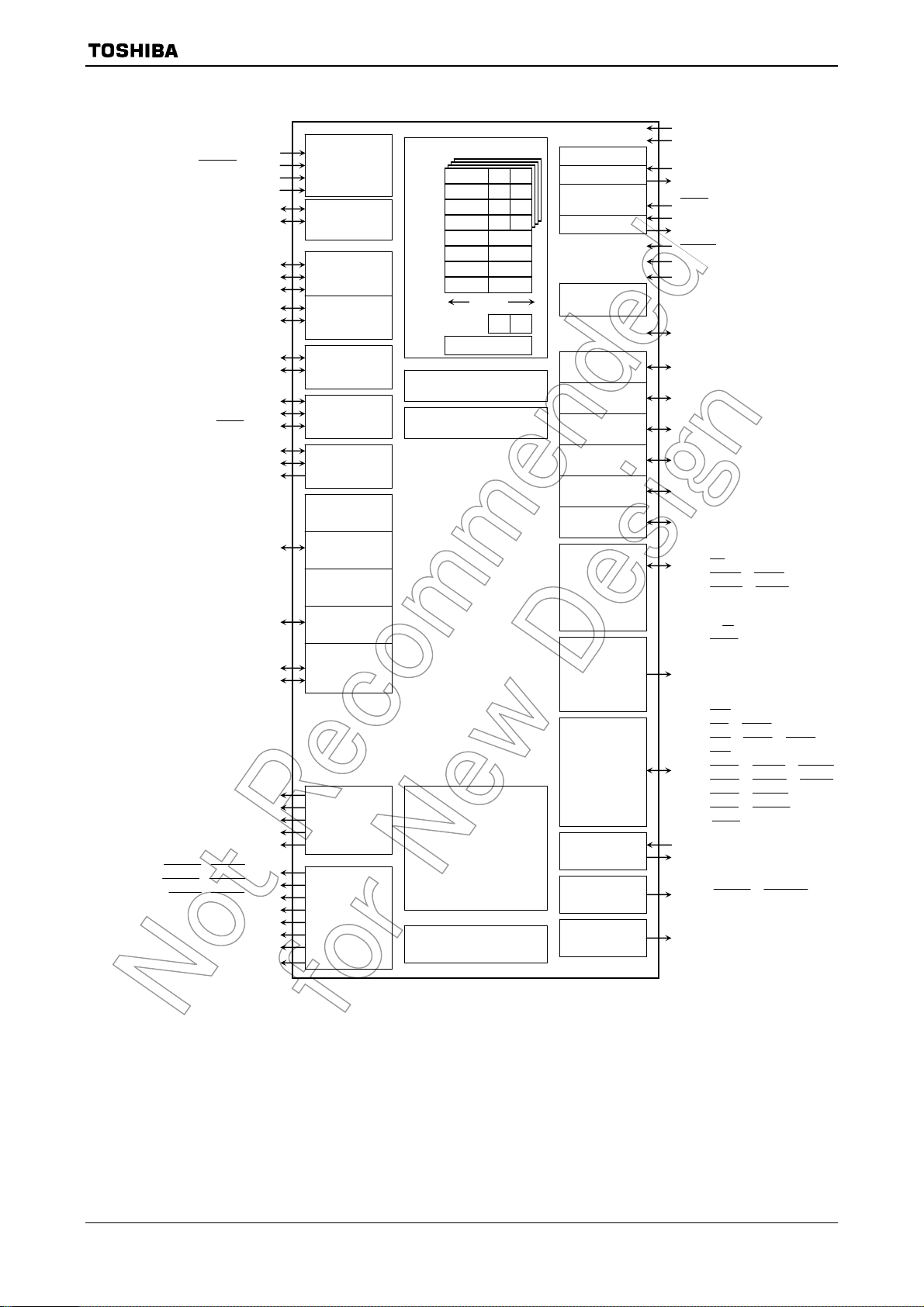
(
)
Y
(
)
A
A
(
,
)
AN3/MY/
(TXD0, TXD1) PF0
(RXD0, RXD1) PF1
(SCLK0,SCLK1) PF2
(I2SCKO, TXD0) P90
(I2SWS, SCLK0,
(I2SDO, RXD0) P91
(LGOE2, CLK32KO) P95
(TA1OUT, INT0) PC0
(TA3OUT, INT1) PC1
(TB0OUT0, INT2) PC2
(
SDRAS ,SRLLB ) PJ0
SDCAS ,SRLUB ) PJ1
(
SDWE ,SRWR ) PJ2
(
(NDALE, SDULDQM) PJ5
(NDCLE, SDUUDQM) PJ6
PG0 to PG1
(AN0 to AN1)
AN2/MX (PG2)
ADTRG (PG3)
AVCC, AVSS
VREFH, VREFL
(PX, INT4) P96
(PY, INT5) P97
D+
D−
0CTS ) P92
(LGOE0) P93
(LGOE1) P94
(INT3) PC3
(LCP0) PK0
(LLP) PK1
(LFR) PK2
(LBCD) PK3
PL0 to PL7
LD0 to LD7
(SDLLDQM) PJ3
(SDLUDQM) PJ4
(SDCKE) PJ7
(SDCLK) PF7
10-bit
4-channel
AD converter
Touch
screen
I/F (TSI)
Serial I/O
SIO0
Serial I/O SIO1
USB
controller
I2S
Port 9
8-bit timer
(TIMERA0)
8-bit timer
(TIMERA1)
8-bit timer
(TIMERA2)
8-bit timer
(TIMERA3)
16-bit timer
(TIMERB0)
LCD
controller
SDRAM
controller
900/H1 CPU
XWA
XBC
XDE
XHL
XIX
XIY
XIZ
XSP
32 bits
SR
Watchdog timer
MMU
16-KB RAM
8-KB mask ROM
(Boot program)
WA
BC
DE
HL
PC
IX
I
IZ
SP
F
PLL
H-OSC
Clock gear
L-OSC
Interrupt
controller
Port 1
Port 2
Port 3
Port 4
Port 5
Port 6
Port 7
NAND flash
I/F (2 channel)
Port 8
Keyboard
I/F
RTC
Melody/
Alarm out
TMP92CH21
DVCC [4]
DVSS [3]
X1
X2
TEST
XT1
XT2
RESET
M0
M1
D0 to D7
P10 to P17
(D8 to D15)
P20 to P27
(D16 to D23, KO0 to KO7)
P30 to P37
(D24 to D31)
P40 to P47
(A0 to A7)
P50 to P57
(A8 to A15)
P60 to P67
(A16 to A23)
RD
P70 (
P71 (
P72 (
P73 (EA24)
P74 (EA25)
P75 (R/
P76 (
P80 (
P81 (
P82 (
P83 (
P84 (
P85 (
P86 (
P87 (
PC7
PA0 to PA7 (KI0 to KI7,
PC6
PM2 (
PM1 (MLDALM)
)
WRLL , NDRE )
WRLU , NDWE )
W , NDR/B)
WAIT )
0CS )
1CS , SDCS )
2CS , CSZA , SDCS )
3CS )
CSZB , WRUL , CE0ND )
CSZC , WRUU , CE1ND )
CSZD , SRULB )
CSZE , SRUUB )
CSZF
LCP1
LD8 to LD11)
KO8, LDIV
ALARM , MLDALM )
Figure 1.1 TMP92CH21 Block Diagram
92CH21-4
2009-06-19
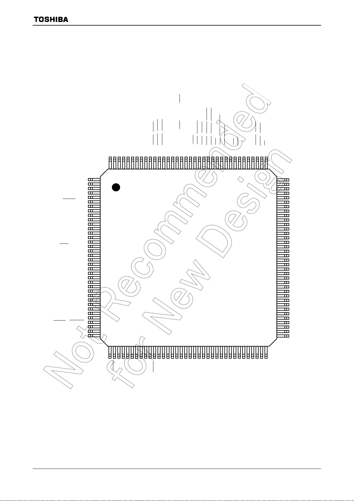
A
2. Pin Assignment and Functions
The assignment of input/output pins for the TMP92CH21FG, their names and functions are
as follows:
2.1 Pin Assignment
SDWE, SRWR
SDCAS, SRLUB
VCC AVSS
PA2, KI2
PA1, KI1
PA0, KI0
PJ7, SDCKE
PJ6, SDUUDQM, NDCLE
PJ5, SDULDQM, NDALE
PJ4, SDLUDQM
PJ3, SDLLDQM
PJ1,
PJ2,
SDRAS, SRLLB
PJ0,
PF7, SDCLK
PC1, TA3OUT, INT1
TMP92CH21
CTS0, SCLK1, CTS1
CSZF, LCP1
CSZE, SRUUB
CSZD, SRULB
CSZC, WRUU, ND1CE
CSZB, WRUL, ND0CE
CS3
CS2, CSZA, SDCS
CS1, SDCS
CS0
WAIT
WRLU, NDWE
WRLL, NDRE
RD
P87,
P84,
P83,
P81,
P75, R/W, NDR/B
PC6, KO8, LDIV
PF1, RXD0, RXD1
PF0, TXD0, TXD1
PC7,
P86,
PC0, TA1OUT, INT0
PF2, SCLK0,
P85,
P82,
P80,
P76,
P74, EA25
P73, EA24
P72,
P71,
P70,
PG0, AN0
PG1, AN1
PG2, AN2, MX
PG3, AN3,
P92, SCLK0,
P95, CLK32KO, LGOE2
PM2,
ADTRG , MY
P96, PX, INT4
P97, PY, INT5
PA3, KI3, LD8
PA4, KI4, LD9
PA5, KI5, LD10
PA6, KI6, LD11
P90, TXD0, I2SCKO
P91, RXD0, I2SDO
P93, LGOE0
P94, LGOE1
PC2, TB0OUT0, INT2
PK0, LCP0
PK3, LBCD
ALARM , MLDALM
PM1, MLDALM
VREFL
VREFH
PA7, KI7
0CTS , I2SWS
PL0, LD0
PL1, LD1
PL2, LD2
PL3, LD3
PL4, LD4
PL5, LD5
PL6, LD6
PL7, LD7
PK1, LLP
PK2, LFR
XT1
XT2
1
5
10
15
20
25
30
35
140
40
135
45
130
125
TMP92CH21FG
QFP144
Top View
50
55
120
60
115
65
70
110
105
100
P67, A23
P66, A22
P65, A21
P64, A20
DVCC3
P63, A19
P62, A18
P61, A17
P60, A16
P57, A15
P56, A14
P55, A13
95
90
85
80
75
P54, A12
P53, A11
P52, A10
P51, A9
P50, A8
P47, A7
P46, A6
P45, A5
P44, A4
P43, A3
P42, A2
P41, A1
P40, A0
P37, D31
P36, D30
DVSS3
P35, D29
P34, D28
P33, D27
P32, D26
P31, D25
P30, D24
P27, D23, KO7
P26, D22, KO6
X1
D+
TEST
DVCC4
X2
D−
DVCC1
AM0
DVSS1
AM1
RESET
PC3, INT3
DVSS2
D0D1D2D3D4D5D6
DVCC2
D7
P10, D8
P11, D9
P12, D10
P13, D11
P14, D12
P15, D13
P16, D14
P17, D15
P20, D16, KO0
P21, D17, KO1
P22, D18, KO2
P23, D19, KO3
P24, D20, KO4
P25, D21, KO5
Figure 2.1.1 Pin Assignment Diagram (144-pin QFP)
92CH21-5
2009-06-19
TMP92CH21
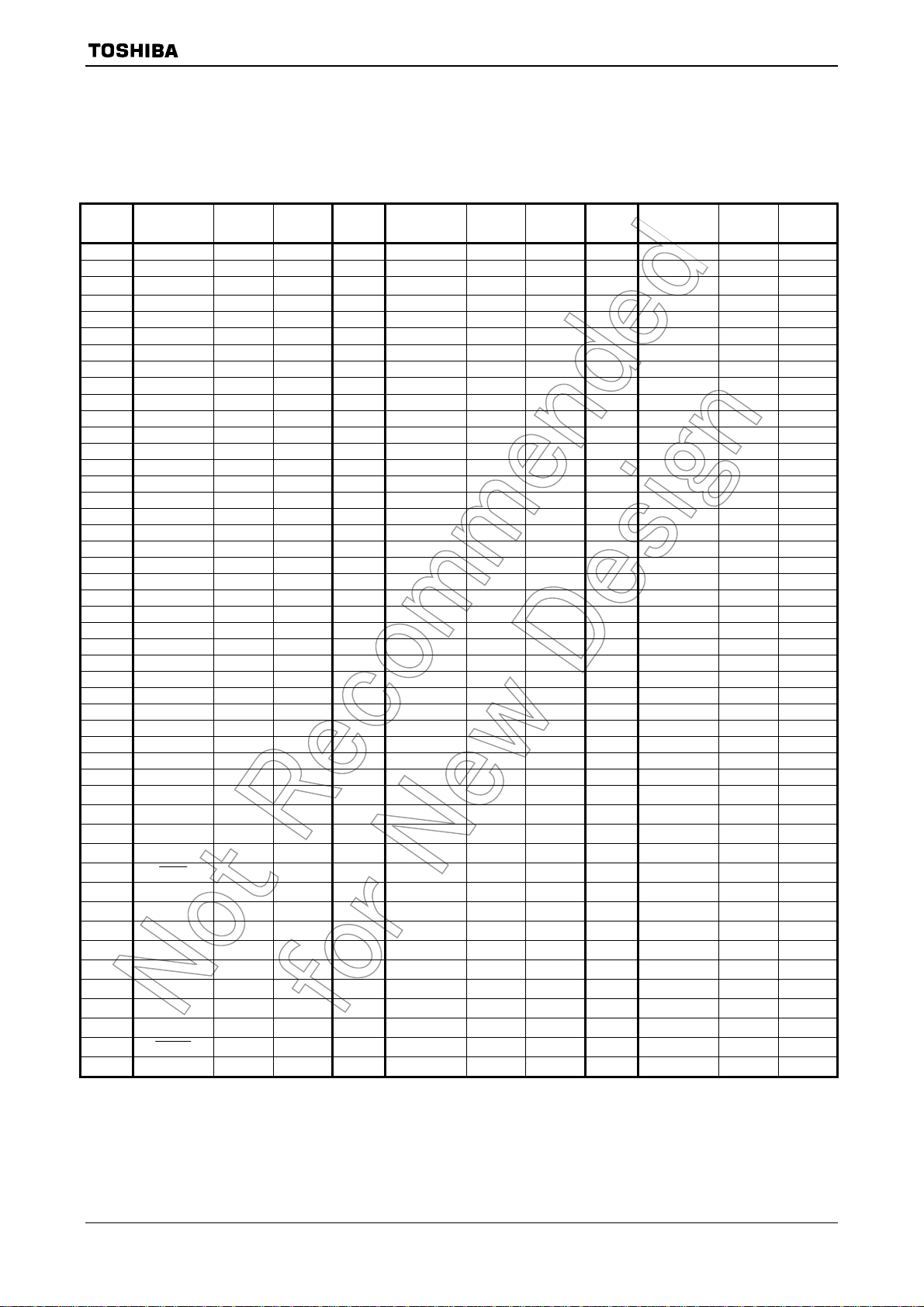
2.2 P AD Assignment
(Chip size 5.98 mm × 6.42 mm)
Table 2.2.1 Pad Assignment Diagram (144-pin chip)
Unit: μm
Pin
No
1
2
3
4
5
6
7 P96 −2852 1920 55 D4 300 −3072 103 P63 2848 1566
8 P97 −2852 1795 56 D5 425 −3072 104 DVCC3 2848 1692
9 PA3
10 PA4 −2852 1145 58 D7 675 −3072 106 P65 2848 1974
11 PA5 −2852 1020 59 P10 800 −3072 107 P66 2848 2130
12 PA6 −2852 895 60 P11 925 −3072 108 P67 2848 2292
13 PA7 −2852 769 61 P12 1050 −3072 109 P70 2460 3065
14 P90 −2852 644 62 P13 1176 −3072 110 P71 2295 3065
15 P91 −2852 519 63 P14 1301 −3072 111 P72 2127 3065
16 P92 −2852 394 64 P15 1426 −3072 112 P73 1964 3065
17 P93 −2852 269 65 P16 1551 −3072 113 P74 1807 3065
18 P94 −2852 144 66 P17 1676 −3072 114 P75 1654 3065
19 P95 −2852 18 67 P20 1801 −3072 115 P76 1506 3065
20 PC2 −2852 −106 68 P21 1927 −3072 116 P80 1361 3065
21 PL0 −2852 −231 69 P22 2052 −3072 117 PC6 1226 3065
22 PL1 −2852 −356 70 P23 2177 −3072 118 P81 1101 3065
23 PL2 −2852 −481 71 P24 2303 −3072 119 P82 976 3065
24 PL3 −2852 −606 72 P25 2460 −3072 120 P83 851 3065
25 PL4
26 PL5 −2852 −857 74 P27 2848 −2138 122 P85 600 3065
27 PL6 −2852 −982 75 P30 2848 −1982 123 P86 475 3065
28 PL7 −2852 −1107 76 P31 2848 −1831 124 P87 350 3065
29 PK0 −2852 −1232 77 P32 2848 −1687 125 PC7 225 3065
30 PK1 −2852 −1357 78 P33 2848 −1562 126 PF0 100 3065
31 PK2 −2852 −1482 79 P34 2848 −1437 127 PF1 −24 3065
32 PK3 −2852 −1608 80 P35 2848 −1311 128 PF2 −150 3065
33 PM2 −2852 −1892 81 DVSS3 2848 −1186 129 PC0 −275 3065
34 PM1
35 XT1
36 XT2
37 DVCC4
38
39 D+
40 D−
41 DVCC1
42 X1
43 DVSS1
44 X2
45 AM0
46 AM1
47
48 PC3
Name
VREFL
VREFH
PG0
PG1
PG2
PG3 −2852 2045
TEST
RESET
X
Point Y Point
−2852 2671 49 DVSS2 −488 −3072 97 P55 2848 815
−2852 2546 50 DVCC2 −338 −3072 98 P56 2848 941
−2852 2421
−2852 2296 52 D1 −75 −3072 100 P60 2848 1191
−2852 2171 53 D2 49 −3072 101 P61 2848 1316
−2852 1270
−2852 −732
−2852 −2017
−2852 −2142
−2852 −2444
−2465 −3072
−2339 −3072
−2062 −3072
−1875 −3072
−1598 −3072
−1472 −3072
−1347 −3072
−1126 −3072
−1001 −3072
−876 −3072
−750 −3072
−625 −3072
Pin
No
51 D0
54 D3
57 D6
73 P26
82 P36
83 P37
84 P40
85 P41
86 P42
87 P43
88 P44
89 P45
90 P46
91 P47
92 P50
93 P51
94 P52
95 P53
96 P54
Name
X
Point Y Point
−200 −3072
174 −3072
550 −3072
2848 −2279
2848 −1061
2848 −936
2848 −811
2848 −686
2848 −560
2848 −435
2848 −310
2848 −185
2848 −60
2848 65
2848 190
2848 315
2848 440
2848 565
2848 690
Pin
No
99 P57
102 P62
105 P64
121 P84
130 PC1 −400 3065
131 PF7 −525 3065
132 PJ0 −650 3065
133 PJ1 −775 3065
134 PJ2 −901 3065
135 PJ3 −1026 3065
136 PJ4 −1151 3065
137 PJ5 −1276 3065
138 PJ6 −1401 3065
139 PJ7 −1526 3065
140 PA0 −1652 3065
141 PA1 −1777 3065
142 PA2 −1902 3065
143 AVSS −2275 3065
144 AVCC −2400 3065
Name
X
Point Y Point
2848 1066
2848 1441
2848 1823
726 3065
92CH21-6
2009-06-19
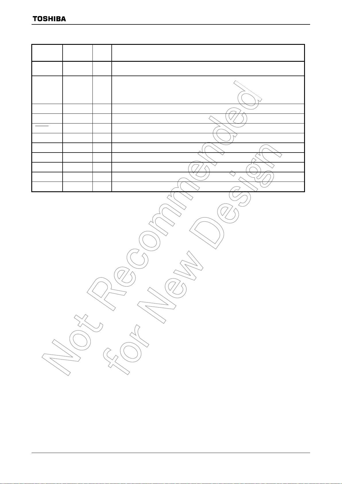
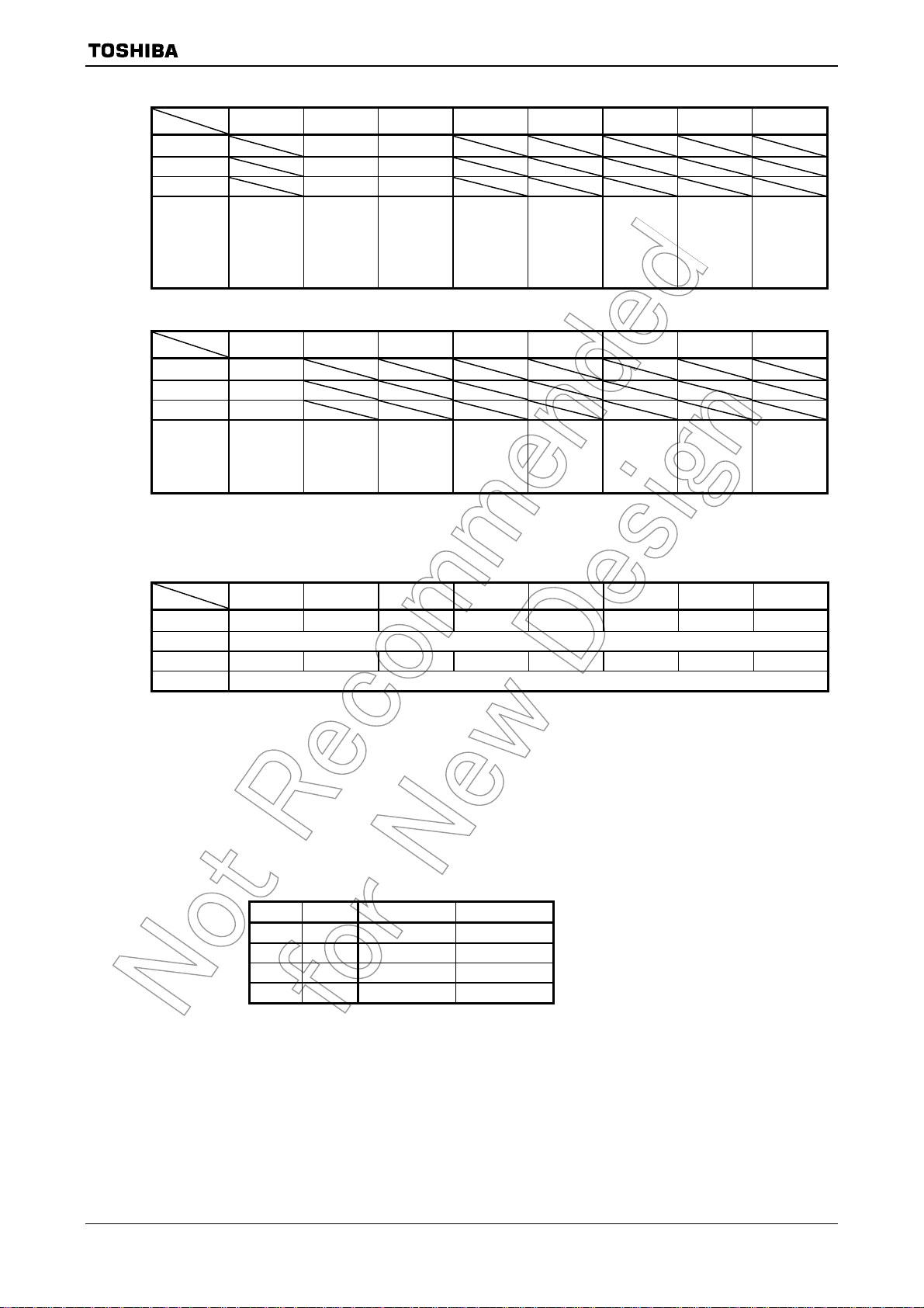
2.3 Pin Names and Functions
The following table shows the names and functions of the input/output pins
Table 2.3.1 Pin Names and Functions (1/5)
TMP92CH21
Pin Name
Number of
I/O Function
Pins
D0 to D7 8 I/O Data: Data bus 0 to 7
P10 to P17
D8 to D15
P20 to P27
D16 to D23
KO0 to KO7
P30 to P37
D24 to D31
P40 to P47
A0 to A7
P50 to P57
A8 to A15
P60 to P67
A16 to A23
P70
RD
P71
WRLL
NDRE
P72
WRLU
NDWE
P73
EA24
P74
EA25
P75
WR/
NDR/B
P76
WAIT
8
8
8
8
8
8
1
1
1
1
1
1
1
I/O
I/O
I/O
I/O
Output
I/O
I/O
Output
Output
Output
Output
I/O
Output
Output
Output
I/O
Output
Output
I/O
Output
Output
Output
Output
Output
Output
I/O
Output
Input
I/O
Input
Port 1: I/O port input or output specifiable in units of bits
Data: Data bus 8 to 15
Port 2: I/O port input or output specifiable in units of bits
Data: Data bus 16 to 23
Key output 0 to 7: Pins used of key-scan strobe (Open-drain output programmable)
Port 3: I/O port input or output specifiable in units of bits
Data24: Data bus 24 to 31
Port 4: Output port
Address: Address bus 0 to 7
Port 5: Output port
Address: Address bus 8 to 15
Port 6: I/O port input or output specifiable in units of bits
Address: Address bus 16 to 23
Port70: Output port
Read: Outputs strobe signal to read external memory
Port 71: I/O port
Write: Output strobe signal for writing data on pins D0 to D7
NAND flash read: Outputs strobe signal to read external NAND flash
Port 72: I/O port
Write: Output strobe signal for writing data on pins D8 to D15
Write Enable for NAND flash
Port 73: Output port
Extended Address 24
Port 74: Output port
Extended Address 25
Port 75: I/O port
Read/Write: 1 represents read or dummy cycle; 0 represents write cycle
NAND flash ready (1)/Busy (0) input
Port 76: I/O port
Wait: Signal used to request CPU bus wait
92CH21-7
2009-06-19
TMP92CH21
Table 2.3.2 Pin Names and Functions (2/5)
Pin Name
P80
0CS
P81
1CS
SDCS
P82
2CS
CSZA
SDCS
P83
3CS
P84
WRUL
CSZB
CE0ND
P85
WRUU
CSZC
CE1ND
P86
CSZD
SRULB
P87
CSZE
SRUUB
P90
TXD0
I2SCKO
P91
RXD0
I2SDO
P92
SCLK0
0CTS
I2SWS
P93
LGOE0
P94
LGOE1
P95
CLK32KO
LGOE2
P96
INT4
PX
P97
INT5
PY
PA0 to PA2
KI0 to KI2
PA3 to PA6
KI3 to KI6
LD8 to LD11
PA7
KI7
Number of
Pins
1
1
1
1
1
1
1
1
1
1
1
1
1
1
1 Input
1 Input
3
4
1
Output
Output
Output
Output
Output
Output
Output
Output
Output
Output
Output
Output
Output
Output
Output
Output
Output
Output
Output
Output
Output
Output
Output
Output
Output
Output
Output
Output
Output
Output
Output
Output
Output
Output
Output
Output
Output
I/O Function
Port80: Output port
Chip select 0: Outputs “low” when address is within specified address area
Port81: Output port
Chip select 1: Outputs “low” when address is within specified address area
Chip select for SDRAM: Outputs “0” when address is within SDRAM address area
Port82: Output port
Chip select 2: Outputs “Low” when address is within specified address area
Expand chip select: ZA: Outputs “0” when address is within specified address area
Chip select for SDRAM: Outputs “0” when address is within SDRAM address area
Port83: Output port
Chip select 3: Outputs “low” when address is within specified address area
Port84: Output port
Write: Output strobe signal for writing data on pins D16 to D23
Expand chip select: ZB: Outputs “0” when address is within specified address area
Chip select for NAND flash 0: Outputs “0” when NAND flash 0 is enabled
Port85: Output port
Write: Output strobe signal for writing data on pins D24 to D31
Expand chip select: ZC: Outputs “0” when address is within specified address area
Chip select for NAND flash 1: Outputs “0” when NAND flash 1 is enabled
Port86: Output port
Expand chip select: ZD: outputs “0” when address is within specified address area
Data enable for SRAM on pins D16 to D23
Port87: Output port
Expand chip select: ZE: Outputs “0” when address is within specified address area
Data enable for SRAM on pins D24 to D31
I/O
Port90: I/O port
Serial 0 send data: Open-drain output programmable
2
I
S clock output
I/O
Port91: I/O port (Schmitt-input)
Input
Input
Input
Input
Input
Input
Input
Input
Input
Input
Serial 0 receive data
2
I
S data output
I/O
Port92: I/O port (Schmitt-input)
I/O
Serial 0 clock I/O
Serial 0 data send enable (Clear to send)
2
I
S word select output
I/O
Port93: I/O port
Output enable-0 for external TFT-LCD driver
I/O
Port94: I/O port
Output enable-1 for external TFT-LCD driver
Port95: Output port
Output fs (32.768 kHz) clock
Output enable-2 for external TFT-LCD driver
Port 96: Input port (Schmitt-input)
Interrupt request pin4: Interrupt request with programmable rising/falling edge
X-Plus: Pin connectted to X+ for touch screen panel
Port 97: Input port (Schmitt-input)
Interrupt request pin5: Interrupt request with programmable rising/falling edge
Y-Plus: Pin connectted to Y+ for touch screen panel
Port: A0 to A2 port: Pin used to input ports (Schmitt input, with pull-up resistor)
Key input 0 to 2: Pin used for key-on wakeup 0 to 2
Port: A3 to A6 port: Pin used to input ports (Schmitt input, with pull-up resistor)
Key input 3 to 6: Pin used for key-on wakeup 3 to 6
Data bus 8 to 11for LCD driver
Port: A7 port: Pin used to input ports (Schmitt input, with pull-up resistor)
Key input 7: Pin used for key-on wakeup 7
92CH21-8
2009-06-19
TMP92CH21
Table 2.3.3 Pin Names and Functions (3/5)
Pin Name
PC0
INT0
TA1OUT
PC1
INT1
TA3OUT
PC2
INT2
TB0OUT0
PC3
INT3
PC6
KO8
LDIV
PC7
CSZF
LCP1
PF0
TXD0
TXD1
PF1
RXD0
RXD1
PF2
SCLK0
0CTS
SCLK1
1CTS
PF7
SDCLK
PG0 to PG1
AN0 to AN1
PG2
AN2
MX
PG3
AN3
MY
ADTRG
Number of
Pins
1
1
1
1
1
1
1
1
1
1
2
1
1
I/O Function
I/O
Port C0: I/O port (Schmitt-input)
Input
Output
Input
Output
Input
Output
Input
Output
Output
Output
Output
Output
Output
Input
Input
Input
Input
Output
Output
Input
Input
Input
Input
Output
Input
Input
Output
Intput
Interrupt request pin 0: Interrupt request pin with programmable level/rising/falling edge
8-bit timer 1 output: Timer 1 output
I/O
Port C1: I/O port (Schmitt-input)
Interrupt request pin 1: Interrupt request pin with programmable rising/falling edge
8-bit timer 3 output: Timer 3 output
I/O
Port C2: I/O port (Schmitt-input)
Interrupt request pin 2: Interrupt request pin with programmable rising/falling edge
Timer B0 output
I/O
Port C3: I/O port (Schmitt-input)
Interrupt request pin 3: Interrupt request pin with programmable rising/falling edge
I/O
Port C6: I/O port
Key Output 8: Pin used of key-scan strobe (Open-drain output programmable)
Data invert enable for external TFT-LCD driver
I/O
Port C7: I/O port
Expand chip select: ZF: Outputs “0” when address is within specified address area
Shift-clock-1 for external TFT-LCD driver
I/O
Port F0: I/O port (Schmitt-input)
Serial 0 send data: Open-drain output programmable
Serial 1 send data: Open-drain output programmable
I/O
Port F1: I/O port (Schmitt-input)
Serial 0 receive data
Serial 1 receive data
I/O
Port F2: I/O port (Schmitt-input)
I/O
Serial 0 clock I/O
Serial 0 data send enable (Clear to send)
I/O
Serial 1 clock I/O
Serial 1 data send enable (Clear to send)
Port F7: Output port
Clock for SDRAM (When SDRAM is not used, SDCLK can be used as system clock)
Port G0 to G1 port: Pin used to input ports
Analog input 0 to 1: Pin used to Input to AD conveter
Port G2 port: Pin used to input ports
Analog input 2: Pin used to Input to AD conveter
X-Minus: Pin connectted to X− for touch screen panel
Port G3 port: Pin used to input ports
Analog input 3: Pin used to input to AD conveter
Y-Minus: Pin connectted to Y− for touch screen panel
AD trigger: Signal used to request AD start
92CH21-9
2009-06-19
TMP92CH21
Table 2.3.4 Pin Names and Functions (4/5)
Pin Name
PJ0
SDRAS
SRLLB
PJ1
SDCAS
SRLUB
PJ2
SDWE
SRWR
PJ3
SDLLDQM
PJ4
SDLUDQM
PJ5
SDULDQM
NDALE
PJ6
SDUUDQM
NDCLE
PJ7
SDCKE
PK0
LCP0
PK1
LLP
PK2
LFR
PK3
LBCD
PL0 to PL3
LD0 to LD3
PL4 to PL7
LD4 to LD7
TEST
PM1
MLDALM
PM2
ALARM
MLDALM
Number of
Pins
1
1
1
1
1
1
1
1
1
1
1
1
4
4
1
1
1
I/O Function
Output
Output
Output
Output
Output
Output
Output
Output
Output
Output
Output
Output
Output
Output
Output
Output
Output
Output
Output
Output
Output
Output
Output
Output
Output
Output
Output
Output
Output
Output
Input Connect to VCC.
Output
Output
Output
Output
Output
Port J0: Output port
Row address strobe for SDRAM
Data enable for SRAM on pins D0 to D7
Port J1: Output port
Column address strobe for SDRAM
Data enable for SRAM on pins D8 to D15
Port J2: Output port
Write enable for SDRAM
Write for SRAM: Strobe signal for writing data
Port J3: Output port
Data enable for SDRAM on pins D0 to D7
Port J4: Output port
Data enable for SDRAM on pins D8 to D15
I/O
Port J5: I/O port
Data enable for SDRAM on pins D16 to D23
Address latch enable for NAND flash
I/O
Port J6: I/O port
Data enable for SDRAM on pins D24 to D31
Command latch enable for NAND flash
Port J7: Output port
Clock enable for SDRAM
Port K0: Output port
LCD driver output pin
Port K1: Output port
LCD driver output pin
Port K2: Output port
LCD driver output pin
Port K3: Output port
LCD driver output pin
Port L0 to L3: Output port
Data bus for LCD driver
I/O
Port L4 to L7: I/O port
Data bus for LCD driver
Port M1: Output port
Melody/alarm output pin
Port M2: Output port
RTC alarm output pin
Melody/alarm output pin (inverted)
Note: The output functions SDULDQM, NDALE of PJ5-pin and SDUUDQM, NDCLE of PJ6-pin cannot be
used simultaneously. Therefore, 32-bit SDRAM and NAND-Flash cannot be used at the same time.
92CH21-10
2009-06-19
TMP92CH21
Table 2.3.5 Pin Names and Functions (5/5)
Pin Name
D+, D− 2 I/O
AM0, AM1 2 Input
X1/X2 2 I/O High-frequency oscillator connection pins
XT1/XT2 2 I/O Low-frequency o scillator connection pins
RESET 1 Input Reset: Initializes TMP92CH21 (with pull-up resistor, Schmitt input)
VREFH 1 Input Pin for reference voltage input to AD converter (H)
VREFL 1 Input Pin for reference voltage input to AD converter (L)
AVCC 1 − Power supply pin for AD converter
AVSS 1 − GND pin for AD converter (0 V)
DVCC 4 − Power supply pins (All VCC pins should be connected to the power supply pin)
DVSS 3 − GND pins (0 V) (All pins should be connected to GND (0 V))
Number of
Pins
I/O Function
USB-data connecting pin
Connect pull-up resistor to both pins to avoid through current when USB is not in use.
Operation mode:
Fix to AM1 = “0”, AM0 = “1” for 16-bit external bus starting
Fix to AM1 = “1”, AM0 = “0” for 32-bit external bus starting
Fix to AM1 = “1”, AM0 = “1” for BOOT (32-bit internal MROM) starting
Note: Use a 9.0 MHz oscillator at pins X1/X2 when USB is used.
92CH21-11
2009-06-19
3. Operation
This section describes the basic components, functions and operation of the TMP92CH21.
3.1 CPU
The TMP92CH21 contains an advanced high-speed 32-bit CPU (TLCS-900/H1 CPU)
3.1.1 CPU Outline
The TLCS-900/H1 CPU is a high-speed, high-performance CPU based on the
TLCS-900/L1 CPU. The TLCS-900/H1 CPU has an expanded 32-bit internal data bus to
process instructions more quickly.
The following is an outline of the CPU:
Table 3.1.1 TMP92CH21 Outline
Parameter TMP92CH21
Width of CPU address bus 24 bits
Width of CPU data bus 32 bits
Internal operating frequency Max 20 MHz
Minimum bus cycle
Internal RAM 32-bit 1-clock access
1-clock access (50 ns at f
= 20MHz)
SYS
TMP92CH21
Internal boot ROM 32-bit 2-clock access
Internal I/O
External SRAM, Masked ROM
External SDRAM 16- or 32-bit min. 1-clock access
External NAND flash
Minimum instruction
execution cycle
Conditional jump
Instruction queue buffer 12 bytes
Instruction set
CPU mode Maximum mode only
Micro DMA 8 channels
8- or 16-bit 2-clock access or
8- or 16-bit 5 to 6-clock access
8- or 16- or 32-bit 2-clock access
(waits can be inserted)
8-bit min. 4-clock access
(waits can be inserted)
1-clock (50 ns at f
2-clock (100 ns at f
Compatible with TLCS-900/L1
(LDX instruction is deleted)
=20MHz)
SYS
=20MHz)
SYS
92CH21-12
2009-06-19
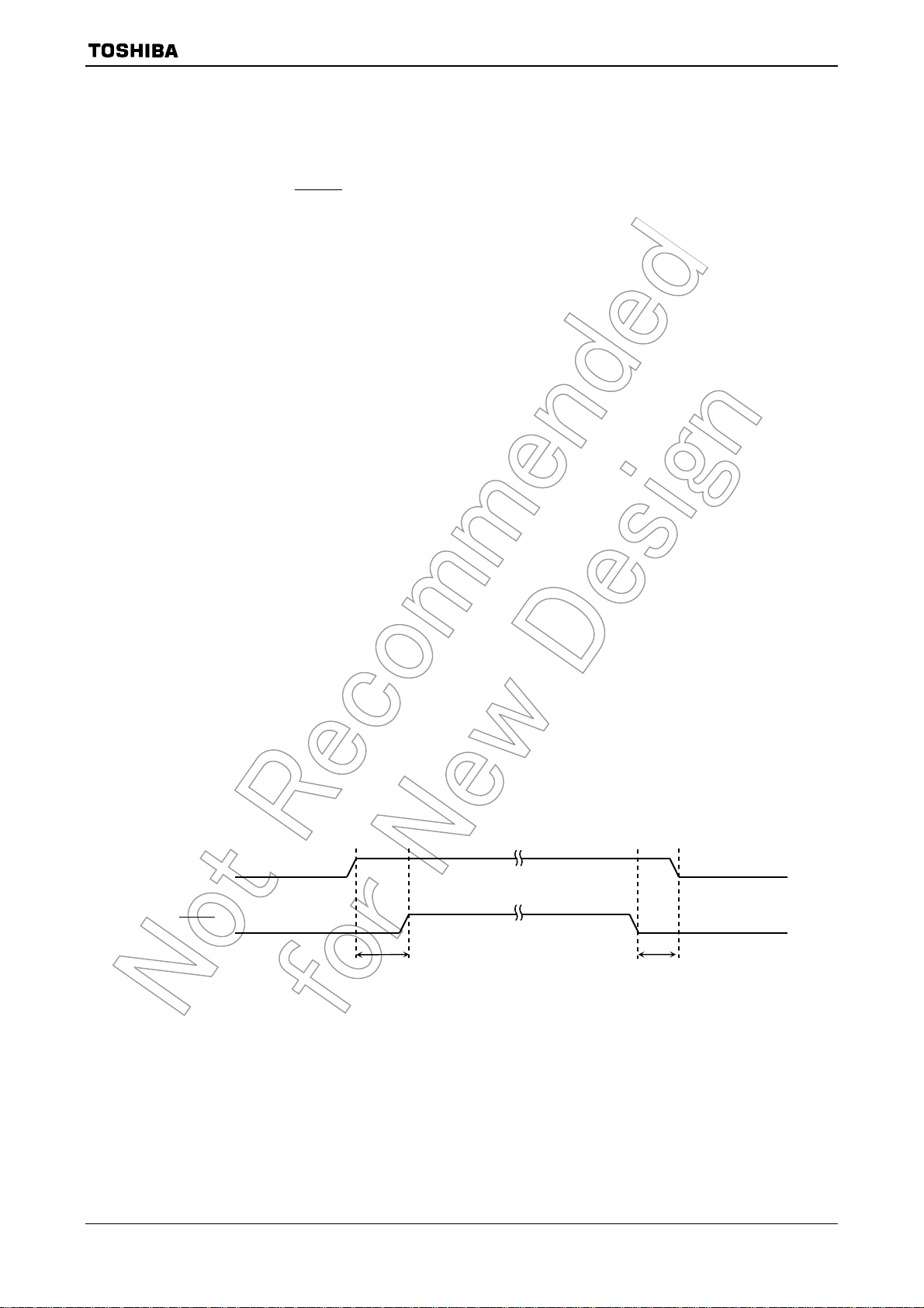
3.1.2 Reset Operation
When resetting the TMP92CH21, ensure that the power supply voltage is within the
operating voltage range, and that the internal high-frequency oscillator has stabilized.
Then hold the
At reset, since the clock doubler (PLL) is bypassed and the clock-gear is set to 1/16, the
system clock operates at 1.25 MHz (fc = 40 MHz).
When the reset has been accepted, the CPU performs the following:
• Sets the program counter (PC) as follows in accordance with the reset vector stored
• Sets the stack pointer (XSP) to 00000000H.
• Sets bits <IFF2:0> of the status register (SR) to 111 (thereby setting the interrupt
• Clears bits <RFP1:0> of the status register to 00 (there by selecting register bank
When the reset is released, the CPU starts executing instructions according to the
program counter settings. CPU internal registers not mentioned above do not change when
the reset is released.
When the reset is accepted, the CPU sets internal I/O, ports and other pins as follows.
• Initializes the internal I/O registers as shown in the “Special Function Register”
RESET
input low for at least 20 system clocks (16 µs at fc = 40 MHz).
at address FFFF00H to FFFF02H:
PC<7:0> ← data in location FFFF00H
PC<15:8> ← data in location FFFF01H
PC<23:16> ← data in location FFFF02H
level mask register to level 7).
0).
table in section 5.
TMP92CH21
• Sets the port pins, including the pins that also act as internal I/O, to
general-purpose input or output port mode.
Internal reset is released as soon as external reset is released.
Memory controller operation cannot be ensured until the power supply becomes stable
after power-on reset. External RAM data provided before turning on the TMP92CH21 may
be corrupted because the control signals are unstable until the power supply becomes
stable after power on reset.
VCC (3.3 V)
RESET
High-frequency oscillation stabilized time
+20 system clock
0 s (Min)
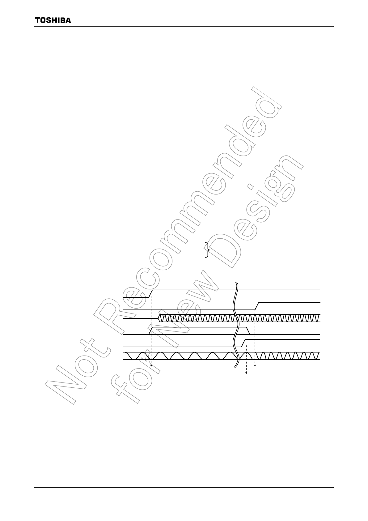
Figure 3.1.1 Power on Reset Timing Example
92CH21-13
2009-06-19

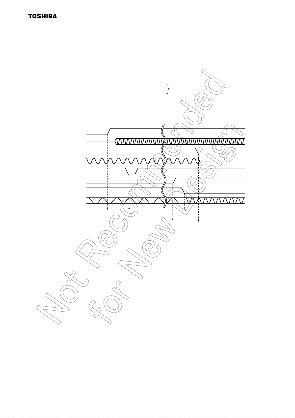
TMP92CH21
Read
Write
0FFFF00H
DATA-IN
((After reset released, starting 1
wait read cycle)
fsys×(13.5~14.5) clock
Pull up (Internal)
High-Z
Sampling
(Output mode)
(Output mode)
(Input mode)
(Input mode)
DATA-IN
DATA-OUT
32-bit external bus (AM1:0=10).
Note: This chart shows timing for a reset using a
sys
RESET
f
A23∼A0
CS2
CS0,1, 3
D0∼D31
RD
SRxxB
D0∼D31
WRxx
SRWR
PF7
SRxxB
PM1~PM2
PJ3~PJ4, PJ7
P40~P47,P50~P57
PL0~PL3
P74~P72, PK0~PK3,
PA0~PA7
P71~P72, P75~P76,
P90~P94, P96~P97,
PJ5~PJ6, PL4~PL7,
PF0~PF1, PG0~PG3,
PC0~PC3, PC6~PC7,
Figure 3.1.2 TMP92CH21 Reset Timing Chart
92CH21-14
2009-06-19
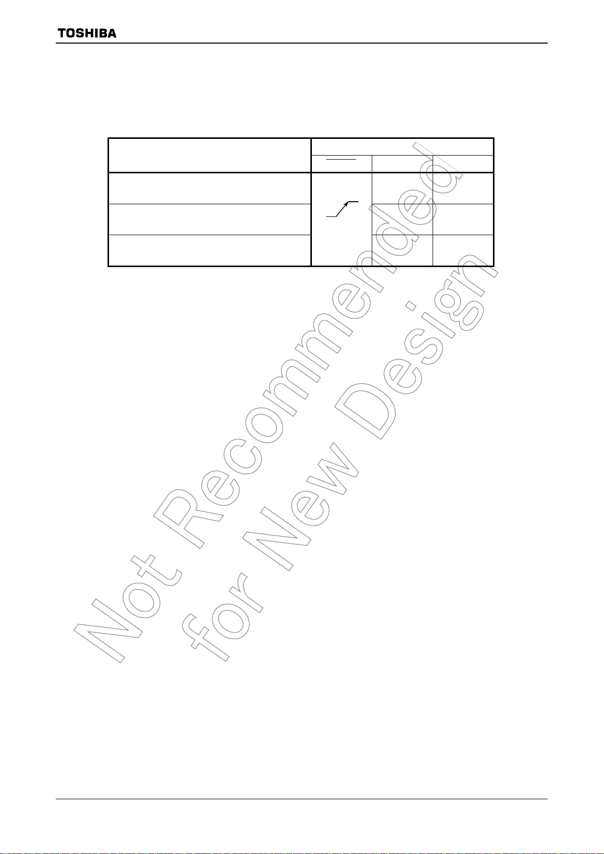
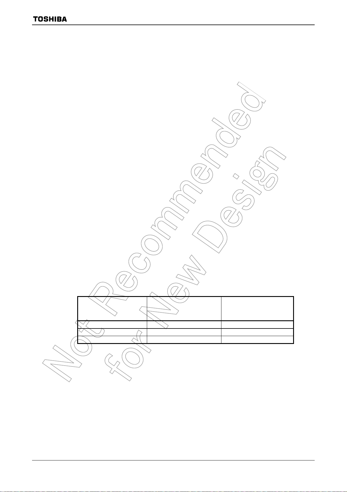
3.1.3 Setting of AM0 and AM1
Set AM1 and AM0 pins as shown in Table 3.1.2 according to system usage.
TMP92CH21
Table 3.1.2 Operation Mode Setup Table
Operation Mode
16-bit external bus starting
(MULTI 16 mode)
32-bit external bus starting
(MULTI 32 mode)
Boot (32-bit internal MROM) starting
(BOOT mode)
Mode Setup Input Pin
RESET AM1 AM0
0 1
1 0
1 1
92CH21-15
2009-06-19
=
3.2 Memory Map
Figure 3.2.1 is a memory map of the TMP92CH21.
000000H
000100H
001D00H
002000H
006000H
Internal I/O
(8 Kbytes)
Internal RAM
(16 Kbytes)
Direct area (n)
64-Kbyte area
(nn)
TMP92CH21
010000H
3FE000H
400000H
F00000H
F10000H
FFFF00H
FFFFFFH
Boot (Internal MROM)
External memory
Provisional emulator control
External memory
Vector table (256 bytes)
(8 Kbytes)
(64 Kbytes)
(Note 1)
(Note 2)
(Note 3)
16-Mbyte area
(R)
(
−R)
+)
(R
+ R8/16)
(R
(R
+ d8/16)
(nnn)
(
Internal area)
Figure 3.2.1 Memory Map
Note 1: Boot program (Internal MROM) is mapped only for BOOT mode. For other starting modes, its area (3FE000H to 3FFFFFH)
is mapped to external-memory.
Note 2: The Provisional emulator control area, mapped F00000H to F0FFFFH after reset, is for emulator use and so is not available.
When emulator
Note 3: Do not use the last 16-byte area (FFFFF0H to FFFFFFH). This area is reserved for an emulator.
WR signal and RD signal are asserted, this area is accessed. Ensure external memory is used.
92CH21-16
2009-06-19

3.3 Clock Function and Stand-by Function
The TMP92CH21 contains (1) clock gear, (2) clock doubler (PLL), (3) stand-by controller and
(4) noise reduction circuits. They are used for low power, low noise systems.
This chapter is organized as follows:
3.3.1 Block diagram of system clock
3.3.2 SFR
3.3.3 System clock controller
3.3.4 Clock doubler (PLL)
3.3.5 Noise reduction circuits
3.3.6 Stand-by controller
TMP92CH21
92CH21-17
2009-06-19
TMP92CH21
The clock operating modes are as follows: (a) single clock mode (X1, X2 pins only), (b) dual
clock mode (X1, X2, XT1 and XT2 pins) and (c) triple clock mode (X1, X2, XT1 and XT2 pins and
PLL).
Figure 3.3.1 shows a transition figure.
Reset
(f
/32)
OSCH
IDLE2 mode
(I/O operate)
IDLE1 mode
(Operate only oscillator)
IDLE2 mode
(I/O operate)
IDLE1 mode
(Operate only oscillator)
IDLE2 mode
(I/O operate)
IDLE1 mode
(Operate only oscillator)
Instruction
Interrupt
Instruction
Interrupt
(f
OSCH
(a) Single clock mode transition figure
Instruction
Interrupt
Instruction
Interrupt
Instruction
Interrupt
NORMAL
(f
OSCH
Instruction
Instruction
Interrupt
(b) Dual clock mode transition figure
Release reset
NORMAL mode
/gear value/2)
Reset
(f
/32)
OSCH
Release reset
mode
/gear value/2)
Interrupt
SLOW mode
(fs/2)
Instruction
Interrupt
Instruction
Interrupt
Instruction
Interrupt
STOP mode
(Stops all circuits)
STOP mode
(Stops all circuits)
STOP mode
(Stops all circuits)
Reset
(f
/32)
NORMAL
(f
OSCH
OSCH
Release reset
mode
/gear value/2)
IDLE2 mode
(I/O operate)
IDLE1 mode
Instruction
Interrupt
Instruction
Interrupt
(Operate only oscillator)
Interrupt
Instruction
Instruction
Note
Instruction
Interrupt
SLOW mode
(fs/2)
Instruction
Interrupt
Instruction
Interrupt
IDLE2 mode
(I/O operate)
IDLE1 mode
(Operate only oscillator)
IDLE2 mode
(I/O operate)
IDLE1 mode
(Operate oscillator and PLL)
Instruction
Interrupt
Instruction
Interrupt
Instruction
Note
NORMAL mode
(4 × f
Using PLL
OSCH
value/2)
Instruction
STOP mode
(Stops all circuits)
/gear
(c) Triple clock mode transition figure
Note 1: It is not possible to control PLL in SLOW mode when shifting from SLOW mode to NORMAL mode with use of PLL.
(PLL start up/stop/change write to PLLCR0<PLLON>, PLLCR1<FCSEL> register)
Note 2: When shifting from NORMAL mode with use of PLL to NORMAL mode, execute the following setting in the same order.
1) Change CPU clock (PLLCR0<FCSEL>
2) Stop PLL circuit (PLLCR1<PLLON>
Note 3: It is not possible to shift from NORMAL mode with use of PLL to STOP mode directly.
NORMAL mode should be set once before shifting to STOP mode. (Sstop the high-frequency oscillator after stopping
PLL.)
← “0”)
← “0”)
Figure 3.3.1 System Clock Block Diagram
The clock frequency input from the X1 and X2 pins is called fc and the clock frequency input from the XT1 and XT2 pins is called
fs. The clock frequency selected by SYSCR1<SYSCK> is called the clock f
clock of f
, and one cycle of f
FPH
is defined as one state.
SYS
92CH21-18
. The system clock f
FPH
is defined as the divided
SYS
2009-06-19
÷2÷16÷
φ
φ
÷
3.3.1 Block Diagram of System Clock
TMP92CH21
SYSCR0<XTEN >
XT1
XT2
X1
X2
Low-frequency
oscillator
SYSCR0<XEN >
High-frequency
oscillator
f
(48 MHz) = f
USB
f
SYS
φT0
f
OSCH
f
IO
OSCH
SYSCR0<WUEF>
SYSCR2<WUPTM1:0>
Warm-up timer
(High/low-frequency oscillator)
Lock up timer
(PLL)
PLLCR1<PLLON>,
fs
Clock doubler
× 16/3
PLLCR0<LUPFG>
f
= f
PLL
OSCH
(PLL)
TMRA0 to 3,TMRB0
Prescaler
SIO0 to SIO1
Prescaler
× 4
Selector
PLLCR0<FCSEL>
USBCR1<USBCLKE>
fc
fc/2
fc/4
fc/8
4
8
Clock-gear
fc/16
SYSCR1<SYSCK>
SYSCR1<GEAR2:0>
USB
Controller
CPU
RAM, ROM
Interrupt
controller
I2S
I/O ports
f
FPH
÷2
LCDC
Memory
controller
NAND flash
controller
TSI
÷4 ÷8
÷2
fs
f
f
IO
T
T0
SYS
RTC
fs
MLD/ALM
ADC
WDT
SDRAMC
Figure 3.3.2 Block Diagram of System Clock
Table 3.3.1 Selection Example for f
High-frequency
Oscillation: f
OSCH
System Clock:
OSCH
f
SYS
(a) USB in use, with PLL 9.0 MHz 18 MHz 48 MHz
(b) USB not in use, with PLL 10.0 MHz (max) 20 MHz (max) −
(c) USB not in use, without PLL
40.0 MHz (max) 20 MHz (max) −
Note: When using USB, the high-frequency oscillator should be 9.0 MHz.
USB Clock: f
USB
92CH21-19
2009-06-19
3.3.2 SFR
SYSCR0
(10E0H)
SYSCR1
(10E1H)
SYSCR2
(10E2H)
TMP92CH21
7 6 5 4 3 2 1 0
Bit symbol XEN XTEN WUEF
Read/Write R/W R/W
Reset state 1 1 0
Function High-
frequency
oscillator
(fc)
0: Stop
1: Oscillation
Lowfrequency
oscillator
(fs)
0: Stop
1: Oscillation
Warm-up
timer
0: Write
don’t care
1: Write
start
timer
0: Read
end
warm-up
1: Read
do not end
warm-up
7 6 5 4 3 2 1 0
Bit symbol SYSCK GEAR2 GEAR1 GEAR0
Read/Write R/W R/W
Reset state 0 1 0 0
Function
Select
system clock
0: fc
1: fs
Select gear value of high-frequency (fc)
000: fc
001: fc/2
010: fc/4
011: fc/8
100: fc/16
101: (Reserved)
110: (Reserved)
111: (Reserved)
7 6 5 4 3 2 1 0
Bit symbol − WUPTM1 WUPTM0 HALTM1 HALTM0
Read/Write R/W R/W R/W R/W R/W
Reset state 0 1 0 1 1
Function Always
write “0”
Warm-up timer
00: Reserved
8
01: 2
/input frequency
14
10: 2
/input frequency
16
11: 2
/input frequency
HALT mode
00: Reserved
01: STOP mode
10: IDLE1 mode
11: IDLE2 mode
Note 1: The unassigned registers, SYSCR0<bit5:3>, SYSCR0<bit1:0>, SYSCR1<bit7:4>, and
SYSCR2<bit6, bit1:0> are read as undefined value.
Note 2: Low-frequency oscillator is enabled on reset.
Figure 3.3.3 SFR for System Clock
92CH21-20
2009-06-19
EMCCR0
(10E3H)
EMCCR1
(10E4H)
EMCCR2
(10E5H)
TMP92CH21
7 6 5 4 3 2 1 0
Bit symbol PROTECT EXTIN
Read/Write R R/W R/W R/W
Reset state 0 0 1 1
Function Protect flag
0: OFF
1: ON
Bit symbol
Read/Write
Reset state
Function
Bit symbol
Read/Write
Reset state
Function
Note: When restarting the oscillator from the stop oscillation state (e.g. restarting the oscillator in STOP mode), set
EMCCR0<DRVOSCH>, <DRVOSCL>=”1”.
Switch the protect ON/OFF by writing the following to 1st-KEY, 2nd-KEY
1st-KEY: write in sequence EMCCR1
2nd-KEY: write in sequence EMCCR1
1: External
clock
= 5AH, EMCCR2 = A5H
= A5H, EMCCR2 = 5AH
DRVOSCH DRVOSCL
fc oscillator
driver ability
1: Normal
0: Weak
fs oscillator
driver ability
1: Normal
0: Weak
Figure 3.3.4 SFR for System Clock
92CH21-21
2009-06-19
PLLCR0
(10E8H)
PLLCR1
(10E9H)
TMP92CH21
7 6 5 4 3 2 1 0
Bit symbol FCSEL LUPFG
Read/Write R/W R
Reset state 0 0
Lock up
timer
status flag
0: Not end
1: End
Function Select fc
clock
0: f
OSCH
1: f
PLL
Note: Ensure that the logic of PLLCR0<LUPFG> is different from 900/L1’s DFM.
7 6 5 4 3 2 1 0
Bit symbol PLLON
Read/Write R/W
Reset state 0
Function Control
on/off
0: OFF
1: ON
PxDR
(xxxxH)
Figure 3.3.5 SFR for PLL
7 6 5 4 3 2 1 0
Bit symbol Px7D Px6D Px5D Px4D Px3D Px2D
Read/Write R/W
Reset state 1 1 1 1 1 1 1 1
Function Output/input buffer drive-register for stand-by mode
(Purpose and use)
This register is used to set each pin status at stand-by mode.
All ports have registers of the format shown above. (“x” indicates the port name.)
For each register, refer to “3.5 Function of ports”.
Before “Halt” instruction is executed, set each register according to the expected pin-status. They will be effective
after the CPU has executed the “Halt” instruction.
This is the case regardless of stand-by mode (IDLE2, IDLE1 or STOP).
The output/input buffer control table is shown below.
OE PxnD Output Buffer Input Buffer
0 0 OFF OFF
0 1 OFF ON
1 0 OFF OFF
1 1 ON OFF
Note 1: OE denotes an output enable signal before stand-by mode.
Basically, PxCR is used as OE.
Note 2: “n” in PxnD denotes the bit number of PORTx.
Px0D
Px1D
Figure 3.3.6 SFR for Drive Register
92CH21-22
2009-06-19
3.3.3 System Clock Controller
TMP92CH21
The system clock controller generates the system clock signal (f
) for the CPU core and
SYS
internal I/O. It contains two oscillation circuits and a clock gear circuit for high-frequency
(fc) operation. The register SYSCR1<SYSCK> changes the system clock to either fc or fs,
SYSCR0<XEN> and SYSCR0<XTEN> control enabling and disabling of each oscillator,
and SYSCR1<GEAR2:0> sets the high-frequency clock gear to either 1, 2, 4, 8 or 16 (fc, fc/2,
fc/4, fc/8 or fc/16). These functions can reduce the power consumption of the equipment in
which the device is installed.
The combination of settings <XEN> = 1, <SYSCK> = 0 and <GEAR2:0> = 100 will cause
the system clock (f
For example, f
) to be set to fc/32 (fc/16 × 1/2) after reset.
SYS
is set to 1.25 MHz when the 40 MHz oscillator is connected to the X1
SYS
and X2 pins.
(1) Switching from normal mode to slow mode
When the resonator is connected to the X1 and X2 pins, or to the XT1 and XT2 pins,
the warm-up timer can be used to change the operation frequency after stable
oscillation has been attained.
The warm-up time can be selected using SYSCR2<WUPTM1:0>.
This warm-up timer can be programmed to start and stop as shown in the following
examples 1 and 2.
Table 3.3.2 shows the warm-up time.
Note 1: When
using an oscillator (other than
a resonator) with stable oscillation, a warm-up
timer is not needed.
Note 2: The warm-up timer is operated by an oscillation clock. Hence, there may be some
variation in warm-up time.
Table 3.3.2 Warm-up Times
at f
Warm-up Time
SYSCR2
<WUPTM1:0>
01 (28/frequency) 6.4 (μs) 7.8 (ms)
10 (214/frequency) 409.6 (μs) 500 (ms)
11 (216/frequency) 1.638 (ms) 2000 (ms)
Change to
Normal Mode
= 40 MHz, fs = 32.768 kHz
OSCH
Change to
Slow Mode
92CH21-23
2009-06-19

1 1 −
X
Example 1: Setting the clock
SYSCR0 EQU 10E0H
SYSCR1 EQU 10E1H
SYSCR2 EQU 10E2H
LD (SYSCR2), 0 X
SET 6, (SYSCR0) ; Enables low-frequency oscillation.
SET 2, (SYSCR0) ; Clears and starts warm-up timer.
WUP: BIT 2, (SYSCR0) ;
JR NZ, WUP ;
SET 3, (SYSCR1) ; Changes f
RES 7, (SYSCR0) ; Disables high-frequency oscillation.
X: Don’t care,
<XEN>
X1, X2 pins
<XTEN>
XT1, XT2 pins
Changing from high-frequency (fc) to low-frequency (fs).
− X
B ; Sets warm-up time to 216/fs.
Detects stopping of warm-up timer.
from fc to fs.
SYS
−: No change
TMP92CH21
Warm-up timer
End of warm-up timer
<SYSCK>
System clock f
SYS
Counts up by f
Enables
low-frequency
Counts up by fs
SYS
fc
Clears and starts
warm-up timer
Chages f
from fc to fs
End of warm-up timer
fs
Disabiles
SYS
high-frequency
92CH21-24
2009-06-19
1 0 −
X
r
r
Example 2: Setting the clock
Changing from low-frequency (fs) to high-frequency (fc).
SYSCR0 EQU 10E0H
SYSCR1 EQU 10E1H
SYSCR2 EQU 10E2H
LD (SYSCR2), 0 X
SET 7, (SYSCR0) ; Enables high-frequency oscillation.
SET 2, (SYSCR0) ; Clears and starts warm-up timer.
WUP: BIT 2, (SYSCR0) ;
JR NZ, WUP ;
RES 3, (SYSCR1) ; Changes f
RES 6, (SYSCR0) ; Disables low-frequency oscillation.
X: Don’t care,
<XEN>
X1, X2 pins
<XTEN>
XT1, XT2 pins
−: No change
− X
B ; Sets warm-up time to 214/fc.
Detects stopping of warm-up timer.
SYS
TMP92CH21
from fs to fc.
Warm-up timer
End of warm-up timer
<SYSCK>
System Clock f
SYS
Counts up by f
Enables
high-frequency
SYS
Clears and starts
warm-up time
Counts up by fc
Changes f
from fs to fc
End of warm-up
time
fcfs
SYS
Disables
low-frequency
92CH21-25
2009-06-19
TMP92CH21
(2) Clock gear controller
f
is set according to the contents of the clock gear select register
FPH
SYSCR1<GEAR2:0> to either fc, fc/2, fc/4, fc/8 or fc/16. Using the clock gear to select a
lower value of f
reduces power consumption.
FPH
Example 3: Changing to a high-frequency gear
SYSCR1 EQU 10E1H
LD (SYSCR1), XXXX0000B ; Changes f
LD (DUMMY), 00H ; Dummy instruction
X: Don’t care
SYS
to fc/2.
(High-speed clock gear changing)
To change the clock gear, write the register value to the SYSCR1<GEAR2:0>
register.It is necessary for the warm-up time to elapse before the change occurs after
writing the register value.
There is the possibility that the instruction following the clock gear changing
instruction is executed by the clock gear before changing.To execute the instruction
following the clock gear switching instruction by the clock gear after changing, input
the dummy instruction as follows (instruction to execute the write cycle).
Example:
SYSCR1 EQU 10E1H
LD (SYSCR1), XXXX0001B ; Changes f
LD (DUMMY), 00H ; Dummy instruction
Instruction to be executed after clock gear has changed
SYS
to fc/4.
92CH21-26
2009-06-19
X X X XX X
X X XX X
A
3.3.4 Clock Doubler (PLL)
TMP92CH21
PLL outputs the f
clock signal, which is four times as fast as f
PLL
OSCH
. A
low-speed-frequency oscillator can be used, even though the internal clock is
high-frequency.
A reset initializes PLL to stop status, so setting to PLLCR0, PLLCR1 register is needed
before use.
As with an oscillator, this circuit requires time to stabilize. This is called the lock up time
and it is measured by a 16-stage binary counter. Lock up time is about 1.6 ms at f
OSCH
= 10
MHz.
Note 1: Input frequency range for PLL
The input frequency range (High-frequency oscillation) for PLL is as follows:
f
= 6 to 10 MHz (VCC = 3.0 to 3.6 V)
OSCH
Note 2: PLLCR0<LUPFG>
The logic of PLLCR0<LUPFG> is different from 900/L1’s DFM.
Exercise care in determining the end of lock up time.
The following is an example of settings for PLL starting and PLL stopping.
Example 1: PLL starting
PLLCR0 EQU 10E8H
PLLCR1 EQU 10E9H
LD (PLLCR1), 1 X
LUP: BIT 5, (PLLCR0) ;
JR Z, LUP ;
LD (PLLCR0), X 1 X
X: Don’t care
B ; Enables PLL operation and starts lock up.
Detects end of lock up.
B ; Changes fc from 10 MHz to 40 MHz.
<PLLON>
<FCSEL>
PLL output: f
Lock up timer
<LUPFG>
System clock f
PLL
SYS
Counts up by f
During lock up
Starts PLL operation and
starts lock up
OSCH
fter lock up
Changes from 10 MHz to 40 MHz
Lock up ends
92CH21-27
2009-06-19
X: Don’t care
Example 2: PLL stopping
PLLCR0 EQU 10E8H
PLLCR1 EQU 10E9H
LD (PLLCR0), X0XXXXXXB ; Changes fc from 40 MHz to10 MHz.
LD (PLLCR1), 0XXXXXXXB ; Stop PLL.
<FCSEL>
<PLLON>
TMP92CH21
PLL output: f
System clock f
PLL
SYS
Changes from 40 MHz to 10 MHz
Stops PLL operation
92CH21-28
2009-06-19

− − −
−
− −
− − − − −
− − −
−
− − − − −
− −
−
− − − − −
− − −
TMP92CH21
Limitations on the use of PLL
1. It is not possible to execute PLL enable/disable control in the SLOW mode (fs)
(writing to PLLCR0 and PLLCR1).
PLL should be controlled in the NORMAL mode.
2. When stopping PLL operation during PLL use, execute the following settings in the
same order.
LD (PLLCR0), 00H ; Change the clock f
LD (PLLCR1), 00H ; PLL stop
PLL
to f
OSCH
3. When stopping the high-frequency oscillator during PLL use, stop PLL before stopping
the high-frequency oscillator.
Examples of settings are shown below:
(1) Start up/change control
(OK) Low-frequency oscillator operation mode (fs) (high-frequency oscillator STOP)
→ High-frequency oscillator start up → High-frequency oscillator operation
mode (f
LD (SYSCR0), 1 1
WUP: BIT 2, (SYSCR0) ;
JR NZ, WUP ;
LD (SYSCR1),
LD (PLLCR1), 1
LUP: BIT 5, (PLLCR0) ;
JR Z, LUP ;
LD (PLLCR0),
) → PLL start up → PLL use mode (f
OSCH
1 −
B ; High-frequency oscillator start/warm-up start
Check for warm-up end flag
− − − −
−
0 −
− − − − − − −
1 −
B ; Change the system clock fs to f
B ; PLL start-up/lock up start
Check for lock up end flag
B ; Change the system clock f
PLL
)
OSCH
OSCH
to f
PLL
(OK) Low-frequency oscillator operation mode (fs) (high-frequency oscillator
Operate) → High-frequency oscillator operation mode (f
→ PLL use mode (f
PLL
)
) → PLL start up
OSCH
LD (SYSCR1), −
LD (PLLCR1), 1
LUP: BIT 5, (PLLCR0) ;
JR Z, LUP
LD (PLLCR0),
−
0 −
− − − − − − −
1 −
− B ; Change the system clock fs to f
B ; PLL start-up/lock up start
Check for lock up end flag
;
B ; Change the system clock f
OSCH
OSCH
to
f
PLL
(Error) Low-frequency oscillator operation mode (fs) (high-frequency oscillator
STOP) → High-frequency oscillator start up → PLL start up → PLL use
mode (f
PLL
)
LD (SYSCR0), 1 1 −
WUP: BIT 2, (SYSCR0) ;
JR NZ, WUP ;
LD (PLLCR1), 1
LUP: BIT 5, (PLLCR0)
JR Z, LUP
LD (PLLCR0),
LD (SYSCR1), −
− − − − − − −
−
1 −
1 −
B ; High-frequency oscillator start/warm-up start
Check for warm-up end flag
B ; PLL start-up/lock up start
;
Check for lock up end flag
;
B ; Change the internal clock f
0 − −
− B ; Change the system clock fs to f
OSCH
to f
PLL
PLL
92CH21-29
2009-06-19

− − − − −
− −
− − − − −
− − −
−
− − − − −
− − −
−
TMP92CH21
(2) Change/stop control
(OK) PLL use mode (f
) → High-frequency oscillator operation mode (f
PLL
OSCH
) →
PLL Stop → Low-frequency oscillator operation mode (fs) → High-frequency
oscillator stop
LD (PLLCR0), − 0 −
LD (PLLCR1), 0
LD (SYSCR1),
LD (SYSCR0), 0
− − − − − − −
− − − −
− − − − − − −
1 −
B ; Change the system clock f
B ; PLL stop
B ; Change the system clock f
B ; High-frequency oscillator stop
PLL
OSCH
to f
OSCH
to fs
(Error) PLL use mode (f
) → Low-frequency oscillator operation mode (fs) → PLL
PLL
stop → High-frequency oscillator stop
LD (SYSCR1), − − − − 1 − − − B ; Change the system clock f
LD (PLLCR0),
LD (PLLCR1), 0
LD (SYSCR0), 0
−
0 −
− − − − − − −
− − − − − − −
B ; Change the internal clock (fC) f
B ; PLL stop
B ; High-frequency oscillator stop
PLL
to fs
PLL
to
f
OSCH
(OK) PLL use mode (f
operation mode (f
) → Set the STOP mode → High-frequency oscillator
PLL
) → PLL stop → Halt (High-frequency oscillator stop)
OSCH
LD (SYSCR2), −
LD (PLLCR0),
LD (PLLCR1), 0
HALT
−
01−
0 −
− − − − − − −
B ; Set the STOP mode
(This command can be executed before use of PLL)
B ; Change the system clock f
B ; PLL stop
; Shift to STOP mode
PLL
to f
OSCH
(Error) PLL use mode (f
) → Set the STOP mode → Halt (High-frequency
PLL
oscillator stop)
LD (SYSCR2), −
HALT
01−
B ; Set the STOP mode
(This command can execute before use of PLL)
; Shift to STOP mode
92CH21-30
2009-06-19

3.3.5 Noise Reduction Circuits
Noise reduction circuits are built-in, allowing implementation of the following features.
(1) Reduced drivability for high-frequency oscillator
(2) Reduced drivability for low-frequency oscillator
(3) Single drive for high-frequency oscillator
(4) SFR protection of register contents
(1) Reduced drivability for high-frequency oscillator
(Purpose)
Reduces noise and power for oscillator when a resonator is used.
(Block diagram)
Resonator
C1
X1 pin
f
OSCH
Enable oscillation
EMCCR0<DRVOSCH>
TMP92CH21
C2
X2 pin
(Setting method)
The drive ability of the oscillator is reduced by writing “0” to
EMCCR0<DRVOSCH> register. At reset, <DRVOSCH> is initialized to “1” and the
oscillator starts oscillation by normal drivability when the power-supply is on.
Note: This function (EMCCR0<DRVOSCH> = “0”) is available when
f
= 6 to 10 MHz.
OSCH
92CH21-31
2009-06-19

TMP92CH21
(2) Reduced drivability for low-frequency oscillator
(Purpose)
Reduces noise and power for oscillator when a resonator is used.
(Block diagram)
C1
Resonator
C2
XT1 pin
Enable oscillation
EMCCR0<DRVOSCL>
fS
XT2 pin
(Setting method)
The drive ability of the oscillator is reduced by writing 0 to the
EMCCR0<DRVOSCL> register. At reset, <DRVOSCL> is initialized to “1”.
(3) Single drive for high-frequency oscillator
(Purpose)
Remove the need for twin drives and prevent operational errors caused by noise
input to X2 pin when an external oscillator is used
.
(Block diagram)
f
OSCH
X1 pin
Enable oscillation
EMCCR0<DRVOSCH>
X2 pin
(Setting method)
The oscillator is disabled and starts operation as buffer by writing “1” to
EMCCR0<EXTIN> register. X2 pin’s output is always “1”.
At reset, <EXTIN> is initialized to “0”.
92CH21-32
2009-06-19

(4) Runaway prevention using SFR protection register
(Purpose)
Prevention of program runaway caused by introduction of noise.
Write operations to a specified SFR are prohibited so that the program is
protected from runaway caused by stopping of the clock or by changes to the
memory control register (memory controller, MMU) which prevent fetch
operations.
Runaway error handling is also facilitated by INTP0 interruption.
Specified SFR list
1. Memory controller
B0CSL/H, B1CSL/H, B2CSL/H, B3CSL/H, BECSL/H
MSAR0, MSAR1, MSAR2, MSAR3,
MAMR0, MAMR1, MAMR2, MAMR3, PMEMCR,
BROMCR
2. MMU
LOCALPX/PY/PZ, LOCALLX/LY/LZ,
LOCALRX/RY/RZ, LOCALWX/WY/WZ,
3. Clock gear
SYSCR0, SYSCR1, SYSCR2, EMCCR0
4. PLL
PLLCR0, PLLCR1
(Operation explanation)
TMP92CH21
Execute and release of protection (write operation to specified SFR) becomes
possible by setting up a double key to EMCCR1 and EMCCR2 registers.
(Double key)
1st KEY: writes in sequence, 5AH at EMCCR1 and A5H at EMCCR2
2nd KEY: writes in sequence, A5H at EMCCR1 and 5AH at EMCCR2
Protection state can be confirmed by reading EMCCR0<PROTECT>.
At reset, protection becomes OFF.
INTP0 interruption also occurs when a write operation to the specified SFR is
executed with protection in the ON state.
92CH21-33
2009-06-19

3.3.6 Stand-by Controller
(1) HALT modes and port drive register
When the HALT instruction is executed, the operating mode switches to IDLE2,
IDLE1 or STOP mode, depending on the contents of the SYSCR2<HALTM1:0> register
and each pin-status is set according to the PxDR register, as shown below:
7 6 5 4 3 2 1 0
PxDR
(xxxxH)
Bit symbol Px7D Px6D Px5D Px4D Px3D Px2D
Read/Write R/W
Reset state 1 1 1 1 1 1 1 1
Function Output/input buffer drive register for stand-by mode
(Purpose and use)
• This register is used to set each pin status at stand-by mode.
• All ports have this registers of the format shown above. (“x” indicates the port name.)
• For each register, refer to 3.5 function of ports.
• Before “Halt” instruction is executed, set each register according to the expected pin status. They will be effective
after the CPU has executed the “Halt” instruction.
• This is the case regardless of stand-by mode (IDLE2, IDLE1 or STOP).
• The Output/Input buffer control table is shown below.
Note 1: OE denotes an output enable signal before stand-by mode.
Basically, PxCR is used as OE.
Note 2: “n” in PxnD denotes the bit number of PORTx
The subsequent actions performed in each mode are as follows:
1. IDLE2: only the CPU halts.
OE PxnD Output Buffer Input Buffer
0 0 OFF OFF
0 1 OFF ON
1 0 OFF OFF
1 1 ON OFF
TMP92CH21
Px0D
Px1D
The internal I/O is available to select operation during IDLE2 mode by setting
the following register.
Table 3.3.3 shows the register settin
g operat
ion during IDLE2 mode.
Table 3.3.3 SFR Setting Operation during IDLE2 Mode
Internal I/O SFR
TMRA01 TA01RUN<I2TA01>
TMRA23 TA23RUN<I2TA23>
TMRB0 TB0RUN<I2TB0>
SIO0 SC0MOD1<I2S0>
SIO1 SC1MOD1<I2S1>
AD converter ADMOD1<I2AD>
WDT WDMOD<I2WDT>
2. IDLE1: Only the oscillator, RTC (real-time clock) and MLD continue to operate.
3. STOP: All internal circuits stop operating.
92CH21-34
2009-06-19

TMP92CH21
The operation of each of the different HALT modes is described in Table 3.3.4.
T
able 3.3.4 I/O Operation duri
ng HALT Modes
HALT Mode IDLE2 IDLE1 STOP
SYSCR2<HALTM1:0> 11 10 01
CPU Stop
I/O ports Depend on PxDR register setting
TMRA, TMRB
Block
SIO
AD converter
WDT
I2S, LCDC, SDRAMC,
Interrupt controller,
USBC,
RTC, MLD
Available to select
operation block
Stop
Operate
Operate
(2) How to release the HALT mode
These halt states can be released by resetting or requesting an interrupt. The halt
release sources are determined by the combination of the states of the interrupt mask
register <IFF2:0> and the HALT modes. The details for releasing the halt status are
shown in Table 3.3.5.
Release by in
terrupt requesting
he HALT mode release method depends on the status of the enabled
T
interrupt .When the interrupt request level set before executing the HALT
instruction exceeds the value of the interrupt mask register, the interrupt is
processed depending on its status after the HALT mode is released, and the CPU
status executing the instruction that follows the HALT instruction. When the
interrupt request level set before executing the HALT instruction is less than the
value of the interrupt mask register, HALT mode release is not executed. (in
non-maskable interrupts, interrupt processing is processed after releasing the
HALT mode regardless of the value of the mask register.) However only for INT0 to
INT4, INTKEY, INTRTC, INTALM and INTUSB interrupts, even if the interrupt
request level set before executing the halt instruction is less than the value of the
interrupt mask register, HALT mode release is executed. In this case, the interrupt
is processed, and the CPU starts executing the instruction following the HALT
instruction, but the interrupt request flag is held at “1”.
Release by resetting
Release of all halt statuses is executed by resetting.
When the STOP mode is released by RESET, it is necessary to allow enough
resetting time (see Table 3.3.6) for operation of the
oscillator to
stabilize.
When releasing the HALT mode by resetting, the internal RAM data keeps the
state before the HALT instruction is executed. However the other settings contents
are initialized. (Releasing due to interrupts keeps the state before the HALT
instruction is executed.)
92CH21-35
2009-06-19

Table 3.3.5 Source of Halt State Clearance and Halt Clearance Operation
TMP92CH21
Status of Received Interrupt
Interrupt Enabled
Interrupt level) ≥ (Interrupt mask)
(
Interrupt Disabled
Interrupt level) < (Interrupt mask)
(
HALT Mode IDLE2 IDLE1 STOP IDLE2 IDLE1 STOP
INTWD ♦ × × − − −
INT0 to INT4 (Note 1) ♦ ♦ ♦*1 ○ ○ ○*1
INTALM0 to INTALM4 ♦ ♦ × ○ ○ ×
INTTA0 to INTTA3,
INTTB0 to INTTB1
INTRX0 to INTRX1,
TX0 to TX1
Interrupt
INTTBO0, INTI2S ♦ × × × × ×
INTAD, INT5 ♦ × × × × ×
INTKEY ♦ ♦ ♦*1 ○ ○ ○*1
INTRTC ♦ ♦ ♦*1 ○ ○ ○*1
Source of Halt State Clearance
INTUSB ♦ ♦*2 × ○ ○*2 ×
INTLCD ♦ × × × × ×
RESET Initialize LSI
♦ × × × × ×
♦ × × × × ×
♦: After clearing the HALT mode, CPU starts interrupt processing.
○: After clearing the HALT m ode, CPU resumes executin g starting from the instruction follo wing the HALT
instruction.
×: Cannot be used to release the HALT mode.
−: The priority level (interrupt request level) of non-maskable interrupts is fixed to 7, the highest priority
level. This combination is not available.
*1: Release of the HALT mode is executed after warm-up time has elapsed.
*2: 6 interrupts of all 24 INTUSB sources can release Halt state from IDLE1 mode, allowing for the
construction of low power dissipation systems. However, the method of use is limited as below.
Shift to IDLE1 mode :
Execute Halt instruction when the flag of INT_SUS or INT_CLKSTOP is “1” ( SUSPEND state )
Release from IDLE1 mode :
Release Halt state by INT_RESUME or INT_CLKON request (release SUSPEND request)
Release Halt state by INT_URST_STR or INT_URST_END request (RESET request)
Example: Releasing IDLE1 mode
An INT0 interrupt clears the halt state when the device is in IDLE1 mode.
Address
8200H LD (PCFC), 01H ; Sets PC0 to INT0.
8203H LD (IIMC), 00H ; Selects INT0 interrupt rising edge.
8206H LD (INTE0AD), 06H ; Sets INT0 interrupt level to 6.
8209H EI 5 ; Sets interrupt level to 5 for CPU.
820BH LD (SYSCR2), 28H ; Sets HALT mode to IDLE1 mode.
820EH HALT ; Halts CPU.
INT0 INT0 interrupt routine
RETI
820FH LD XX, XX
92CH21-36
2009-06-19

r
TMP92CH21
(3) Operation
1. IDLE2 mode
In IDLE2 mode only specific internal I/O operations, as designated by the
IDLE2 setting register, can take place. Instruction execution by the CPU stops.
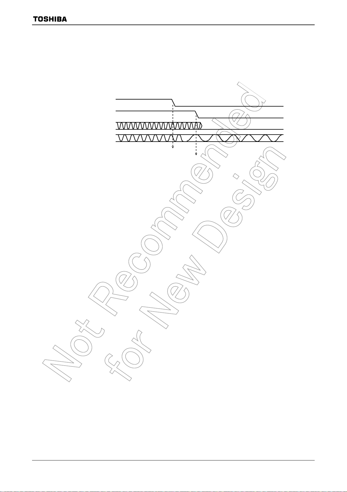
Figure 3.3.7 illustrates an example of the timing for clearance of the IDLE2
de halt state by an interrupt.
mo
X1
A0 to A23
D0 to D31
RD
WR
Interrupt for
release
Figure 3.3.7
Data
IDLE2
mode
Timing Chart for IDLE2 Mode Halt State Cleared by Interrupt
Data
2. IDLE1 mode
In IDLE1 mode, only the internal oscillator and the RTC and MLD continue to
operate. The system clock stops.
In the halt state, the interrupt request is sampled asynchronously with the
system clock; however, clearance of the halt state (e.g., restart of operation) is
synchronous with it.
Figure 3.3.8 illustrates the timing for clearance of the IDLE1 mode halt state by
an interrupt.
X1
A0 to A23
D0 to D31
RD
WR
Interrupt fo
release
Figure 3.3.8 Timing Char
Data
IDLE1
mode
t for IDLE1 Mode Halt State Cleared by Interrupt
92CH21-37
Data
2009-06-19

r
3. STOP mode
oscillator.
warm-up time has elapsed, in order to allow oscillation to stabilize.
an interrupt.
TMP92CH21
When STOP mode is selected, all internal circuits stop, including the internal
After STOP mode has been cleared system clock output starts when the
Figure 3.3.9 illustrates the timing for clearance of the STOP mode halt state by
Warm-up time
X1
A0 to A23
D0 to D31
Data
Data
RD
WR
Interrupt fo
release
STOP
mode
Figure 3.3.9 T
iming Chart for STOP Mode Halt State Cleared by Interrupt
Table 3.3.6 Example of Warm-up Time after Releasing STOP Mode
at f
SYSCR1
<SYSCK>
0 (fc) 6.4 μs 409.6 μs 1.638 ms
1 (fs) 7.8 ms 500 ms 2000 ms
8
) 10 (214) 11 (216)
01 (2
SYSCR2<WUPTM1:0>
= 40 MHz, fs = 32.768 kHz
OSCH
92CH21-38
2009-06-19

TMP92CH21
Table 3.3.7 Input Buffer State Table
Input Buffer State
In HALT mode (IDLE1/2/STOP)
<PxDR>
as
= 1 <PxDR> = 0
When used
as
Input pin
When used
as
Function pin
When used
Input pin
as
Port Name
Input
Function
Name
During
Reset
When the CPU is
operating
When used
as
Function pin
When used
as
Input pin
When used
Function pin
D0 to D7 D0 to D7 OFF − OFF − OFF −
P10 to P17 D8 to D15
P20 to P27 D16 to D23
P30 to P37 D24 to D31
P60 to P67 −
P71 to P72 −
P75
NDRB
P76 WAIT
16bit start : OFF
32bit start : OFF
Boot start : ON
16bit start : ON
32bit start : OFF
Boot start : ON
16bit start : OFF
32bit start : OFF
Boot start : ON
ON upon
external
read
OFF OFF
− − −
ON ON OFF
P90 − − − −
P91 RXD0
P92
CTS0,
SCLK0
P93 to P94 − − − −
1
*
P96
INT4
P97 INT5
1
PA0 to PA7
*
KI0-KI7
ON
PC0 INT0
ON ON OFF
ON
ON
OFF
ON ON OFF
PC1 INT1
PC2 INT2
PC3 INT3
PC6 to PC7 −
PF0 −
− − −
PF1 RXD0/1
PF2
PG0 to PG2
*
PG3
PJ5 to PJ6 −
PL4 to PL7 −
CTS0/1
SCLK0/1
2
*
− − − −
2
ADTRG
OFF
ON
ON
ON upon
ON
port read
− ON − ON −
ON: The buffer is always turned on. A current flows through the input
buffer if the input pin is not driven.
OFF:
The buffer is always turned off.
ON
ON
OFF
OFF
ON
*1: Port having a pull-up/pull-down resistor.
*2: AIN input does not cause a current to flow through the
buffer.
−: Not applicable
92CH21-39
2009-06-19

TMP92CH21
Table 3.3.8 Output Buffer St ate Table (1/2)
Output Buffer State
When the CPU is
operating
When used
as
Function pin
When used
as
Output pin
When used
Function pin
Port Name
Output
Function
Name
During
Reset
D0~D7 D0~D7 − − −
P10~P17 D8~D15
P20~P27
D16~D23,
KO0~KO7
OFF
ON upon
external
write
P30~P37 D24~D31
P40~P47 A0-A7
P50~P57 A8~A15
P60~P67 A16~A23
P70
P71
P72
RD
WRLL, NDRE
,
NDWE
WRLU
P73 EA24
P74 EA25
P75 R/W
P76 −
P80
P81
P82
P83
P84
P85
P86
P87
CSZB
CSZC, WRUU
CSZD,SRULB
CSZE,SRUUB
0CS
,
1CS
SDCS
,
,
2CS
CSZA
SDCS
3CS
,
,
WRUL
CE0ND
,
CE1ND
ON
OFF
ON
OFF
ON
ON ON
− − −
ON ON OFF
ON
P90 TXD0, I2SCKO
P91 I2SDO
P92 SCLK0, I2SWS
OFF
P93 LGOE0
P94 LGOE1
P95
1
*
P96
PX
P97 PY
LGOE2,
CLK32KO
ON
OFF
−
ON:
The buffer is always turned on. *1: Port having a pull-up/pull-down resistor.
OFF:
The buffer is always turned off.
−: Not applicable
In HALT mode (IDLE1/2/STOP)
<PxDR>=1 <PxDR>=0
as
When used
as
Output pin
When used
as
Function pin
When used
Output pin
as
OFF
OFF
ON
−
OFF
−
92CH21-40
2009-06-19

TMP92CH21
Table 3.3.9 Output Buffer St ate Table (2/2)
Output Buffer State
Port
Name
PA3~PA6
*
PC0 TA1OUT
PC1 TA3OUT
PC2 TB0OUT0
PC3 − − − −
PC6 KO8, LDIV
PC7
PF0 TXD0, TXD1
PF1 − − − −
PF2 SCLK0, SCLK1
PF7 SDCLK ON
PG2 MX
PG3 MY
PJ0
PJ1
PJ2
PJ3 SDLLDQM
PJ4 SDLUDQM
PJ5
PJ6
PJ7 SDCKE
PK0 LCP0
PK1 LLP
PK2 LFR
PK3 LBCD
PL0~PL3 LD0~LD3
PL4~PL7 LD4~LD7 OFF
PM1 MLDALM
PM2
X2 −
Output
Function
Name
1
LD8~LD11 − − −
During
Reset
OFF
, LCP1
CSZF
OFF − − −
SDRAS,SRLLB
SDCAS,SRLUB
SDWE,SRWR
SDULDQM,
NDALE
SDUUDQM,
NDCLE
ON
OFF
ON
,
MLDALM
ALARM
ON
When the CPU is
operating
When used
as
Function pin
When used
as
Output pin
When used
Function pin
ON ON OFF
ON ON OFF
ON
ON ON OFF
ON ON
−
XT2 −
ON:
The buffer is always turned on. *1: Port having a pull-up/pull-down resistor.
OFF:
The buffer is always turned off.
−: Not applicable
In HALT mode (IDLE1/2/STOP)
<PxDR>=1 <PxDR>=0
as
When used
as
Output pin
When used
as
Function pin
When used
as
Output pin
OFF
ON
OFF
IDLE2/1:ON,
−
STOP: output ”H”
IDLE2/1:ON,
STOP: output ”HZ”
92CH21-41
2009-06-19

3.4 Interrupts
Interrupts are controlled by the CPU Interrupt mask register <IFF2:0> (bits12 to 14 of the
status register) and by the built-in interrupt controller.
The TMP92CH21 has a total of 50 interrupts divided into the following five types:
A fixed individual interrupt vector number is assigned to each interrupt source.
Any one of six levels of priority can also be assigned to each maskable interrupt.
Non-maskable interrupts have a fixed priority level of 7, the highest level.
When an interrupt is generated, the interrupt controller sends the priority of that interrupt
to the CPU. When more than one interrupt is generated simultaneously, the interrupt
controller sends the priority value of the interrupt with the highest priority to the CPU. (The
highest priority level is 7, the level used for non-maskable interrupts.)
The CPU compares the interrupt priority level which it receives with the value held in the
CPU interrupt mask register <IFF2:0>. If the priority level of the interrupt is greater than or
equal to the value in the interrupt mask register, the CPU accepts the interrupt.
However, software interrupts and illegal instruction interrupts generated by the CPU are
processed irrespective of the value in <IFF2:0>.
The value in the interrupt mask register <IFF2:0> can be changed using the EI instruction
(EI num sets <IFF2:0> to num). For example, the command EI 3 enables the acceptance of all
non-maskable interrupts and of maskable interrupts whose priority level, as set in the
interrupt controller, is 3 or higher. The commands EI and EI 0 enable the acceptance of all
non-maskable interrupts and of maskable interrupts with a priority level of 1 or above (hence
both are equivalent to the command EI 1).
The DI instruction (sets <IFF2:0> to 7) is exactly equivalent to the EI 7 instruction. The DI
instruction is used to disable all maskable interrupts (since the priority level for maskable
interrupts ranges from 1 to 6). The EI instruction takes effect as soon as it is executed.
In addition to the general purpose interrupt processing mode described above, there is also a
micro DMA processing mode.
In micro DMA mode the CPU automatically transfers data in one-byte, two-byte or four-byte
blocks; this mode allows high-speed data transfer to and from internal and external memory
and internal I/O ports.
In addition, the TMP92CH21 also has a software start function in which micro DMA
processing is requested in software rather than by an interrupt.
Figure 3.4.1 is a flowchart showing overall interrupt processing.
TMP92CH21
Interrupts generated by CPU: 9 sources
Software interrupts: 8 sources
Illegal instruction interrupt: 1 source
Internal interrupts: 34 sources
Internal I/O interrupts: 26 sources
Micro DMA transfer end interrupts: 8 sources
External interrupts: 7 sources
Interrupts on external pins (INT0 to INT5, INTKEY)
92CH21-42
2009-06-19

TMP92CH21
Interrupt processing
Micro DMA soft
start request
Interrupt specified
by micro DMA
start vector ?
NO
YES
Clear interrupt request flag
General-purpose
interrupt
processing
Interrupt vector calue “V”
read interrupt request F/F clear
PUSH PC
PUSH SR
SR<IFF2:0> ← Level of
INTNEST ← INTNEST + 1
PC ← (FFFF00H + V)
accepted
interrupt + 1
Data transfer by micro
DMA
COUNT ← COUNT − 1
COUNT = 0
NO
Micro DMA
processing
YES
Clear vector register
generating micro DMA
transfer end interrupt
(INTTC0 to 7)
Interrupt processing
program
RETI instruction
POP SR
POP PC
INTNEST ← INTNEST − 1
End
Figure 3.4.1 Interrupt and Micro DMA Processing Sequence
92CH21-43
2009-06-19

3.4.1 General-purpose Interrupt Processing
When the CPU accepts an interrupt, it usually performs the following sequence of
operations. However, in the case of software interrupts and illegal instruction interrupts
generated by the CPU, the CPU skips steps (1) and (3), and executes only steps (2), (4) and
(5).
(1) The CPU reads the interrupt vector from the interrupt controller.
When more than one interrupt with the same priority level has been generated
simultaneously, the interrupt controller generates an interrupt vector in accordance
with the default priority and clears the interrupt requests.
(The default priority is determined as follows: the smaller the vector value, the
higher the priority.)
(2) The CPU pushes the program counter (PC) and status register (SR) onto the top of the
stack (pointed to by XSP).
(3) The CPU sets the value of the CPU’s interrupt mask register <IFF2:0> to the priority
level for the accepted interrupt plus 1. However, if the priority level for the accepted
interrupt is 7, the register’s value is set to 7.
TMP92CH21
(4) The CPU increments the interrupt nesting counter INTNEST by 1.
(5) The CPU jumps to the address given by adding the contents of address FFFF00H + the
interrupt vector, then starts the interrupt processing routine.
On completion of interrupt processing, the RETI instruction is used to return control to
the main routine. RETI restores the contents of the program counter and the status
register from the stack and decrements the interrupt nesting counter INTNEST by 1.
Non-maskable interrupts cannot be disabled by a user program. Maskable interrupts,
however, can be enabled or disabled by a user program. A program can set the priority level
for each interrupt source. (A priority level setting of 0 or 7 will disable an interrupt
request.)
If an interrupt request is received for an interrupt with a priority level equal to or greater
than the value set in the CPU interrupt mask register <IFF2:0>, the CPU will accept the
interrupt. The CPU interrupt mask register <IFF2:0> is then set to the value of the priority
level for the accepted interrupt plus 1.
If during interrupt processing, an interrupt is generated with a higher priority than the
interrupt currently being processed, or if, during the processing of a non-maskable
interrupt processing, a non-maskable interrupt request is generated from another source,
the CPU will suspend the routine which it is currently executing and accept the new
interrupt. When processing of the new interrupt has been completed, the CPU will resume
processing of the suspended interrupt.
If the CPU receives another interrupt request while performing processing steps (1) to (5),
the new interrupt will be sampled immediately after execution of the first instruction of its
interrupt processing routine. Specifying DI as the start instruction disables nesting of
maskable interrupts.
A reset initializes the interrupt mask register <IFF2:0> to 111, disabling all maskable
interrupts.
Table 3.4.1 shows the TMP92CH21 interrupt vectors and micro DMA start vectors.
FFFF00H to FFFFFFH (256 bytes) is designated as the interrupt vector area.
92CH21-44
2009-06-19

Table 3.4.1 TMP92CH21 Interrupt Vectors and Micro DMA St art Vectors
TMP92CH21
Default
Priority
1
2 [SWI1] instruction 0004H FFFF04H
3 Illegal instruction or [SWI2] instruction 0008H FFFF08H
4 [SWI3] instruction 000CH FFFF0CH
5 [SWI4] instruction 0010H FFFF10H
6 [SWI5] instruction 0014H FFFF14H
7 [SWI6] instruction 0018H FFFF18H
8 [SWI7] instruction 001CH FFFF1CH
9 (Reserved) 0020H FFFF20H
10
− Micro DMA − − − (Note1)
11 INT0: INT0 pin input 0028H FFFF28H 0AH (Note 2)
12 INT1: INT1 pin input 002CH FFFF2CH 0BH
13 INT2: INT2 pin input 0030H FFFF30H 0CH
14 INT3: INT3 pin input 0034H FFFF34H 0DH
15 INT4: INT4 pin input (TSI) 0038H FFFF38H 0EH
16 INTALM0: ALM0 (8192Hz) 003CH FFFF3CH 0FH
17 INTALM1: ALM1 (512 Hz) 0040H FFFF40H 10H
18 INTALM2: ALM2 (64 Hz) 0044H FFFF44H 11H
19 INTALM3: ALM3 (2 Hz) 0048H FFFF48H 12H
20 INTALM4: ALM4 (1 Hz) 004CH FFFF4CH 13H
21 INTP0: Protect0 (Write to special SFR) 0050H FFFF50H 14H
22 (Reserved) 0054H FFFF54H 15H
23 INTTA0: 8-bit timer 0 0058H FFFF58H 16H
24 INTTA1: 8-bit timer 1 005CH FFFF5CH 17H
25 INTTA2: 8-bit timer 2 0060H FFFF60H 18H
26 INTTA3: 8-bit timer 3 0064H FFFF64H 19H
27 INTTB0: 16-bit timer 0 0068H FFFF68H 1AH
28 INTTB1: 16-bit timer 0 006CH FFFF6CH 1BH
29 INTKEY: Key-on wakeup 0070H FFFF70H 1CH
30 INTRTC: RTC (Alarm interrupt) 0074H FFFF74H 1DH
31 INTTBO0: 16-bit timer 0 (Overflow) 0078H FFFF78H 1EH
32 INTLCD: LCDC/LP pin 007CH FFFF7CH 1FH
33 INTRX0: Serial receive (Channel 0) 0080H FFFF80H 20H (Note 2)
34 INTTX0: Serial transmission (Channel 0) 0084H FFFF84H 21H
35 INTRX1: Serial receive (Channel 1) 0088H FFFF88H 22H (Note 2)
36 INTTX1: Serial transmission (Channel 1) 008CH FFFF8CH 23H
37 (Reserved) 0090H FFFF90H 24H
38 (Reserved) 0094H FFFF94H 25H
39 INT5: INT5 pin input 0098H FFFF98H 26H
40 INTI2S: I2S (Channel 0) 009CH FFFF9CH 27H
41 INTNDF0 (NAND flash controller channel 0) 00A0H FFFFA0H 28H
42 INTNDF1 (NAND flash controller channel 1) 00A4H FFFFA4H 29H
43 (Reserved) 00A8H FFFFA8H 2AH
44 (Reserved) 00ACH FFFFACH 2BH
45 (Reserved)
46 (Reserved) 00B4H FFFFB4H 2DH
47 (Reserved) 00B8H FFFFB8H 2EH
48 INTUSB: USB 00BCH FFFFBCH 2FH
49 (Reserved) 00C0H FFFFC0H 30H
50
Type
Reset or [SWI0] instruction 0000H FFFF00H
Nonmaskable
INTWD: Watchdog Timer 0024H FFFF24H
Maskable
(Reserved) 00C4H FFFFC4H 31H
Interrupt Source and Source of
Micro DMA Reque st
Vector
Value
00B0H FFFFB0H 2CH
Address Refer
to Vector
Micro
DMA Start
Vector
92CH21-45
2009-06-19

TMP92CH21
Default
Priority
51 (Reserved) 00C8H FFFFC8H 32H
52 INTAD: AD conversion end 00CCH FFFFCCH 33H
53 INTTC0: Micro DMA end (Channel 0) 00D0H FFFFD0H 34H
54 INTTC1: Micro DMA end (Channel 1) 00D4H FFFFD4H 35H
55 INTTC2: Micro DMA end (Channel 2) 00D8H FFFFD8H 36H
56 INTTC3: Micro DMA end (Channel 3) 00DCH FFFFDCH 37H
57 INTTC4: Micro DMA end (Channel 4) 00E0H FFFFE0H 38H
58 INTTC5: Micro DMA end (Channel 5) 00E4H FFFFE4H 39H
59 INTTC6: Micro DMA end (Channel 6) 00E8H FFFFE8H 3AH
60 INTTC7: Micro DMA end (Channel 7) 00ECH FFFFECH 3BH
−
to
−
Type
Maskable
(Reserved)
Interrupt Source and Source of
Micro DMA Reque st
Vector
Value
00F0H
:
00FCH
Address Refer
to Vector
FFFFF0H
:
FFFFFCH
Micro
DMA Start
Vector
−
to
−
Note 1: Micro DMA default priority.
Micro DMA initiation takes priority over other maskable interrupts.
Note 2: When initiating micro DMA, set at edge detect mode.
92CH21-46
2009-06-19

3.4.2 Micro DMA Processing
In addition to general purpose interrupt processing, the TMP92CH21 also includes a
micro DMA function. Micro DMA processing for interrupt requests set by micro DMA is
performed at the highest priority level for maskable interrupts (level 6), regardless of the
priority level of the interrupt source.
Because the micro DMA function is implemented through the CPU, when the CPU is
placed in a stand-by state by a Halt instruction, the requirements of the micro DMA will be
ignored (pending).
Micro DMA supports 8 channels and can be transferred continuously by specifying the
micro DMA burst function as below.
Note: When using the micro DMA transfer end interrupt, always write “1” to bit 7 of SIMC register.
(1) Micro DMA operation
When an interrupt request is generated by an interrupt source specified by the micro
DMA start vector register, the micro DMA triggers a micro DMA request to the CPU at
interrupt priority level 6 and starts processing the request. The eight micro DMA
channels allow micro DMA processing to be set for up to eight types of interrupt at
once.
When micro DMA is accepted, the interrupt request flip-flop assigned to that
channel is cleared. Data in one-byte, two-byte or four-byte blocks, is automatically
transferred at once from the transfer source address to the transfer destination
address set in the control register, and the transfer counter is decremented by 1. If the
value of the counter after it has been decremented is not 0, DMA processing ends with
no change in the value of the micro DMA start vector register. If the value of the
decremented counter is 0, a micro DMA transfer end interrupt (INTTC0 to INTTC7) is
sent from the CPU to the interrupt controller. In addition, the micro DMA start vector
register is cleared to 0, the next micro DMA operation is disabled and micro DMA
processing terminates.
If micro DMA requests are set simultaneously for more than one channel, priority is
not based on the interrupt priority level but on the channel number: the lower the
channel number, the higher the priority (channel 0 thus has the highest priority and
channel 7 the lowest).
If an interrupt request is triggered for the interrupt source in use during the interval
between the time at which the micro DMA start vector is cleared and the next setting,
general purpose interrupt processing is performed at the interrupt level set. Therefore,
if the interrupt is only being used to initiate micro DMA (and not as a general-purpose
interrupt), the interrupt level should first be set to 0 (i.e., interrupt requests should be
disabled).
TMP92CH21
If micro DMA and general purpose interrupts are being used together as described
above, the level of the interrupt which is being used to initiate micro DMA processing
should first be set to a lower value than all the other interrupt levels. (Note) In this
case, edge triggered interrupts are the only kinds of general interrupts which can be
accepted.
Note: If the priority level of micro DMA is set higher than that of other interrupts, CPU operates as follows.
In case INTxxx interrupt is generated first and then INTyyy interrupt is generated between checking
“Interrupt specified by micro DMA start vector” (in the Figure 3.4.1) and reading interrupt vector with
setting below. The vector shifts to that of INT
This is because the priority level of INTyyy is higher than that of INTxxx.
In the interrupt routine, CPU reads the vector of INTyyy because cheking of micro DMA has finished.
And INTyyy is generated regardless of transfer counter of micro DMA.
INTxxx: level 1 without micro DMA
INTyyy: level 6 with micro DMA
yyy at the time.
92CH21-47
2009-06-19

A
TMP92CH21
Although the control registers used for setting the transfer source and transfer
destination addresses are 32 bits wide, this type of register can only output 24-bit
addresses. Accordingly, micro DMA can only access 16 Mbytes (the upper eight bits of a
32-bit address are not valid).
Three micro DMA transfer modes are supported: one-byte transfers, two-byte
(one-word) transfer and four-byte transfer. After a transfer in any mode, the transfer
source and transfer destination addresses will either be incremented or decremented,
or will remain unchanged. This simplifies the transfer of data from memory to memory,
from I/O to memory, from memory to I/O, and from I/O to I/O. For details of the various
transfer modes, see section 3.4.2 (1), detailed description of the transfer mode register.
Since a transfer counter is a 16-bit counter, up to 65536 micro DMA processing
operations can be performed per interrupt source (provided that the transfer counter
for the source is initially set to 0000H).
Micro DMA processing can be initiated by any one of 34 different interrupts – the 33
interrupts shown in the micro DMA start vectors in Table 3.4.1 and a micro DMA soft
start.
Figure 3.4.2 shows a 2-byte transfer carried out us
ing a micro
DMA cycle in transfer
destination address INC mode (micro DMA transfers are the same in every mode
except counter mode). (The conditions for this cycle are as follows: Both source and
destination memory are internal RAM and multiples by 4 numbered source and
destination addresses.)
1 state
(1)
fSYS
23 to A0
Note: In fact, src and dst address are not output to A23 to A0 pins
because they are internal RAM address.
(2) (3) (4) (5)
src
dst
Figure 3.4.2 Timing for Micro DMA Cycle
State (1), (2):
State (3):
State (4):
Instruction fetch cycle (Prefetches the next instruction code)
Micro DMA read cycle
Micro DMA write cycle
State (5): (The same as in state (1), (2))
92CH21-48
2009-06-19

TMP92CH21
(2) Soft start function
The TMP92CH21 can initiate micro DMA either with an interrupt or by using the
micro DMA soft start function, in which micro DMA is initiated by a write cycle which
writes to the register DMAR.
Writing 1 to any bit of the register DMAR causes micro DMA to be performed once.
(If write “0” to each bit, micro DMA doesn’t operate). On completion of the transfer, the
bits of DMAR which support the end channel are automatically cleared to 0.
Only one channel can be set once for DMA request. (Do not write “1” to plural bits.)
When writing again 1 to the DMAR register, check whether the bit is “0” before
writing “1”. If read “1”, micro DMA transfer isn’t started yet.
When a burst is specified by the DMAB register, data is transferred continuously
from the initiation of micro DMA until the value in the micro DMA transfer counter is 0.
If execatee soft start during micro DMA transfer by interrupt source, micro DMA
transfer counter doesn’t change. Don’t use Read-modify-write instruction to avoid
writign to other bits by mistake.
Symbol Name Address 7 6 5 4 3 2 1 0
DREQ7 DREQ6 DREQ5 DREQ4 DREQ3 DREQ2 DREQ1 DREQ0
R/W
0 0 0 0 0 0 0 0
1: DMA request in software
DMAR
DMA
Request
109H
(Prohibit
RMW)
(3) Transfer control registers
The transfer source address and the transfer destination address are set in the
following registers. An instruction of the form LDC cr, r can be used to set these
registers.
Channel 0
DMAS0 DMA source address register 0
DMAD0 DMA destination address register 0
DMAC0 DMA counter register 0
DMAM0 DMA mode regis t er 0
Channel 7
DMAS7 DMA source address register 7
DMAD7 DMA destination address register 7
DMAC7 DMA counter register 7
DMAM7 DMA mode regis t er 7
32 bits
8 bits
16 bits
92CH21-49
2009-06-19

(4) Detailed description of the transfer mode register
0 0 0 Mode
DMAMn[4:0] Mode Description
0 0 0 z z Destination INC mode
(DMADn+) ← (DMASn)
DMACn ← DMACn − 1
If DMACn = 0 then INTTCn
0 0 1 z z Destination DEC mode
(DMADn−) ← (DMASn)
DMACn ← DMACn − 1
If DMACn = 0 then INTTCn
0 1 0 z z Source INC mode
(DMADn) ← (DMASn+)
DMACn ← DMACn − 1
If DMACn = 0 then INTTCn
0 1 1 z z Source DEC mode
(DMADn) ← (DMASn−)
DMACn ← DMACn − 1
If DMACn = 0 then INTTCn
1 0 0 z z Source and destination INC mode
(DMADn+) ← (DMASn+)
DMACn ← DMACn − 1
If DMACn = 0 then INTTCn
1 0 1 z z Source and destination DEC mode
(DMADn−) ← (DMASn−)
DMACn ← DMACn − 1
If DMACn = 0 then INTTCn
1 1 0 z z Source and destination Fixed mode
(DMADn) ← (DMASn)
DMACn ← DMACn − 1
If DMACn = 0 then INTTCn
1 1 1 0 0 Counter mode
DMASn ← DMASn + 1
DMACn ← DMACn − 1
If DMACn = 0 then INTTCn
ZZ: 00 = 1-byte transfer
01 = 2-byte transfer
10 = 4-byte transfer
11 = (Reserved)
DMAM0 to DMAM7
TMP92CH21
Execution
State Number
5 states
5 states
5 states
5 states
6 states
6 states
5 states
5 states
Note1: N stands for the micro DMA channel number (0 to 7)
DMADn+/DMASn+: Post-increment (register value is incremented after transfer)
DMADn−/DMASn−: Post-decrement (register value is decremented after transfer)
“I/O” signifies fixed memory addresses; “memory” signifies incremented or decremented memory
addresses.
Note2: The transfer mode register should not be set to any value other than those listed above.
Note3: The execution state number shows number of best case (1-state memory access).
92CH21-50
2009-06-19

3.4.3 Interrupt Controller Operation
The block diagram in Figure 3.4.3 shows the interrupt circuits. The left hand side of the
diagram shows the interrupt controller circuit. The right hand side shows the CPU
interrupt request signal circuit and the halt release circuit.
For each of the 52 interrupts channels there is an interrupt request flag (consisting of a
flip-flop), an interrupt priority setting register and a micro DMA start vector register. The
interrupt request flag latches interrupt requests from the peripherals. The flag is cleared to
zero in the following cases: when a reset occurs, when the CPU reads the channel vector of
an interrupt it has received, when the CPU receives a micro DMA request (when micro
DMA is set), when a micro DMA burst transfer is terminated, and when an instruction that
clears the interrupt for that channel is executed (by writing a micro DMA start vector to the
INTCLR register).
An interrupt priority can be set independently for each interrupt source by writing the
priority to the interrupt priority setting register (e.g., INTE0AD or INTE12). 6 interrupt
priorities levels (1 to 6) are provided. Setting an interrupt source’s priority level to 0 (or 7)
disables interrupt requests from that source. The priority of non-maskable interrupt
(watchdog timer interrupts) is fixed at 7. If more than one interrupt request with a given
priority level are generated simultaneously, the default priority (the interrupt with the
lowest priority or, in other words, the interrupt with the lowest vector value) is used to
determine which interrupt request is accepted first.
The 3rd and 7th bit of the interrupt priority setting register indicate the state of the
interrupt request flag and thus whether an interrupt request for a given channel has
occurred.
If several interrupts are generated simultaneously, the interrupt controller sends the
interrupt request for the interrupt with the highest priority and the interrupt’s vector
address to the CPU. The CPU compares the mask value set in <IFF2:0> of the status
register (SR) with the priority level of the requested interrupt; if the latter is higher, the
interrupt is accepted. Then the CPU sets SR<IFF2:0> to the priority level of the accepted
interrupt + 1. Hence, during processing of the accepted interrupt, new interrupt requests
with a priority value equal to or higher than the value set in SR<IFF2:0> (e.g., interrupts
with a priority higher than the interrupt being processed) will be accepted.
When interrupt processing has been completed (e.g., after execution of a RETI
instruction), the CPU restores to SR<IFF2:0> the priority value which was saved on the
stack before the interrupt was generated.
The interrupt controller also includes eight registers which are used to store the micro
DMA start vector. Writing the start vector of the interrupt source for the micro DMA
processing (see Table 3.4.1), enables the corresponding interrupts to be processed by micro
DM
A proc
DMAS and DMAD) prior to micro DMA processing.
essing. The values must be set in the micro DMA parameter registers (e.g.,
TMP92CH21
92CH21-51
2009-06-19

g
r
A
r
r
A
i
t
t
7
During
STOP
During
IDLE1
Halt release
TMP92CH21
Micro DMA request
Micro DMA channel
specification
3
INTALM, INTUSB
if IFF = 7 then 0
RESET
Interrupt
mask F/F
Interrupt request
signal
EI 1 to 7
DI
Interrupt
level detect
3
3
If INTRQ2 to 0 ≥ IFF
2 to 0 then 1.
RESET
INT01 to INT4, INTKEY,INTRTC,
IFF2 to 0
D2
D3
D4
D5
D6
generator
Interrupt vector
D7
Interrupt vector
read
8 input OR
8
3
A
B
C
0 1 2 3 4 5 6
7
priority decoder
Micro DMA channel
1
nal to CPU
Interrupt request
si
Priority encoder
INTRQ2 to 0
3
A
B
C
Highest
priority
interrupt
1 2 3 4 5
level select
7
6
1
D0
D1
6
45
6
Interrupt controller CPU
V = 20H
V = 24H
Decode
Y1
V = 28H
V = 30H
V = 2CH
Y2
Y3
Y4
Y5
Y6
Dn + 3
B
C
V = 40H
V = 44H
V = 34H
V = 38H
V = 48H
V = 3CH
V = D0H
V = 4CH
V = E0H
V = E4H
V = D4H
V = D8H
V = E8H
V = DCH
V = ECH
Soft start
:
DMA0V
DMA1V
DMA7V
S
Selector
6
51
Interrupt request F/F
Interrupt request F/F
S Q
R
RESET
Priority setting register
errup
n
Dn
vector read
CLR
D Q
Dn + 1
Dn + 2
Interrupt vector read
S Q
Micro DMA acknowledge
R
D Q
Interrupt
request F/F
D5
D4
D3
Reset
D2
Micro DMA start vector setting registe
CLR
D1
D0
INTTC0
RESET
INTTC0
INTTC1
INTTC2
INTTC3
INTTC4
INTTC5
INTTC6
zero
interrupt
INTTC7
INTWD
INT0
INT1
INT2
INT3
INT4
INTALM0
INTALM1
INTALM2
INTALM3
INTALM4
counte
Micro DM
Figure 3.4.3 Block Diagram of Interrupt Controller
92CH21-52
2009-06-19

TMP92CH21
(1) Interrupt level setting registers
Symbol Name Address 7 6 5 4 3 2 1 0
INTAD INT0
INT2 INT1
INT4 INT3
INTI2S INT5
INTTA1 (TMRA 1) INTTA0 (TM RA 0)
INTTA3 (TMRA 3) INTTA2 (TM RA 2)
INTTB1 (TMRA 4) INTTB0 (TM RA 4)
− INTTBO0
R R/W
Note: Always write 0 0 0 0 0
INTTX0 INTRX0
INTTX1 INTRX1
− INTUSB
R R/W
Note: Always write 0 0
INTALM1 INTALM0
INTALM3 INTALM2
INTE0AD
INTE12
INTE34
INTE5I2S
INTETA01
INTETA23
INTETB01
INTETBO0
INTES0
INTES1
INTEUSB
INTEALM01
INTEALM23
INT0
&
INTAD
enable
INT1
&
INT2
enable
INT3
&
INT4
enable
INT5
&
INTI2S
enable
INTTA0
&
INTTA1
enable
INTTA2
&
INTTA3
enable
INTTB0
&
INTTB1
enable
INTTBO0
(Overflow)
enable
INTRX0
&
INTTX0
enable
INTRX1
&
INTTX1
enable
INTUSB
enable
INTALM0 &
INTALM1
enable
INTALM2 &
INTALM3
enable
F0H
D0H
D1H
EBH
D4H
D5H
D8H
DAH
DBH
DCH
E3H
E5H
E6H
IADC IADM2 IADM1 IADM0 I0C I0M2 I0M1 I0M0
R R/W R R/W
0 0 0 0 0 0 0 0
I2C I2M2 I2M1 I2M0 I1C I1M2 I1M1 I1M0
R R/W R R/W
0 0 0 0 0 0 0 0
I4C I4M2 I4M1 I4M0 I3C I3M2 I3M1 I3M0
R R/W R R/W
0 0 0 0 0 0 0 0
II2SC II2SM2 II2SM1 II2SM0 I5C I5M2 I5M1 I5M0
R R/W R R/W
0 0 0 0 0 0 0 0
ITA1C ITA1M2 ITA1M1 ITA1M0 ITA0C ITA0M2 ITA0M1 ITA0M0
R R/W R R/W
0 0 0 0 0 0 0 0
ITA3C ITA3M2 ITA3M1 ITA3M0 ITA2C ITA2M2 ITA2M1 ITA2M0
R R/W R R/W
0 0 0 0 0 0 0 0
ITB1C ITB1M2 ITB1M1 ITB1M0 ITB0C ITB0M2 ITB0M1 ITB0M0
R R/W R R/W
0 0 0 0 0 0 0 0
− − − − ITBO0C ITBO0M2 ITBO0M1 ITBO0M0
ITX0C ITX0M2 ITX0M1 ITX0M0 IRX0C IRX0M2 IRX0M1 IRX0M0
R R/W R R/W
0 0 0 0 0 0 0 0
ITX1C ITX1M2 ITX1M1 ITX1M0 IRX1C IRX1M2 IRX1M1 IRX1M0
R R/W R R/W
0 0 0 0 0 0 0 0
− − − − IUSB0C IUSBM2 IUSBM1 IUSBM0
IA1C IA1M2 IA1M1 IA1M0 IA0C IA0M2 IA0M1 IA0M0
R R/W R R/W
0 0 0 0 0 0 0 0
IA3C IA3M2 IA3M1 IA3M0 IA2C IA2M2 IA2M1 IA2M0
R R/W R R/W
0 0 0 0 0 0 0 0
92CH21-53
2009-06-19

TMP92CH21
Symbol Name Address 7 6 5 4 3 2 1 0
− INTALM4
INTEALM4
INTERTC
INTEKEY
INTELCD
INTEND01
INTEP0
INTALM4
enable
INTRTC
enable
INTKEY
enable
INTLCD
enable
INTNDF0
&
INTNDF1
enable
INTP0
enable
E7H
E8H
E9H
EAH
ECH
EEH
− − − − IA4C IA4M2 IA4M1 IA4M0
R R/W
Note: Always write 0 0 0 0 0
− INTRTC
− − − − IRC IRM2 IRM1 IRM0
R R/W
Note: Always write 0 0 0 0 0
− INTKEY
− − − − IKC IKM2 IKM1 IKM0
R R/W
Note: Always write 0 0 0 0 0
− INTLCD
− − − − ILCD1C ILCDM2 ILCDM1 ILCDM0
R R/W
Note: Always write 0 0 0 0 0
INTNDF1 INTNDF0
IN1C IN1M2 IN1M1 IN1M0 IN0C IN0M2 IN0M1 IN0M0
R R/W R R/W
0 0 0 0 0 0 0 0
− INTP0
− − − − IP0C IP0M2 IP0M1 IP0M0
R R/W
Note: Always write 0 0 0 0 0
lxxM2 lxxM1 lxxM0 Function (Write)
0 0 0 Disables interrupt requests
0 0 1 Sets interrupt priority level to 1
0 1 0 Sets interrupt priority level to 2
0 1 1 Sets interrupt priority level to 3
Interrupt request flag
1 0 0 Sets interrupt priority level to 4
1 0 1 Sets interrupt priority level to 5
1 1 0 Sets interrupt priority level to 6
1 1 1 Disables interrupt requests
92CH21-54
2009-06-19
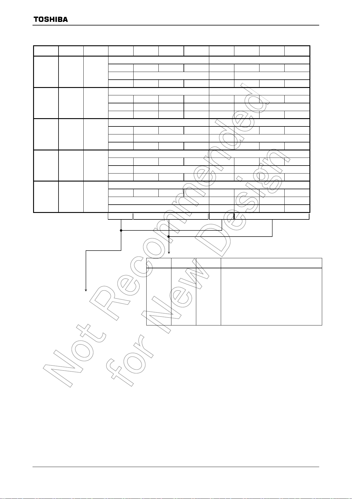
TMP92CH21
Symbol Name Address 7 6 5 4 3 2 1 0
INTTC1 (DMA1) INTTC0 (DMA0)
INTTC3 (DMA3) INTTC2 (DMA2)
INTTC5 (DMA5) INTTC4 (DMA4)
INTTC7 (DMA7) INTTC6 (DMA6)
− INTWD
R
Note: Always write 0 0 − − −
INTETC01
INTETC23
INTETC45
INTETC67
INTWDT
INTTC0
&
INTTC1
enable
INTTC2
&
INTTC3
enable
INTTC4
&
INTTC5
enable
INTTC6 &
INTTC7
enable
INTWD
enable
F1H
F2H
F3H
F4H
F7H
ITC1C ITC1M2 ITC1M1 ITC1M0 ITC0C ITC0M2 ITC0M1 ITC0M0
R R/W R R/W
0 0 0 0 0 0 0 0
ITC3C ITC3M2 ITC3M1 ITC3M0 ITC2C ITC2M2 ITC2M1 ITC2M0
R R/W R R/W
0 0 0 0 0 0 0 0
ITC5C ITC5M2 ITC5M1 ITC5M0 ITC4C ITC4M2 ITC4M1 ITC4M0
R R/W R R/W
0 0 0 0 0 0 0 0
ITC7C ITC7M2 ITC7M1 ITC7M0 ITC6C ITC6M2 ITC6M1 ITC6M0
R R/W R R/W
0 0 0 0 0 0 0 0
− − − − ITCWD − − −
lxxM2 lxxM1 lxxM0 Function (Write)
0 0 0 Disables interrupt requests
0 0 1 Sets interrupt priority level to 1
0 1 0 Sets interrupt priority level to 2
0 1 1 Sets interrupt priority level to 3
Interrupt request flag
1 0 0 Sets interrupt priority level to 4
1 0 1 Sets interrupt priority level to 5
1 1 0 Sets interrupt priority level to 6
1 1 1 Disables interrupt requests
92CH21-55
2009-06-19

TMP92CH21
(2) External interrupt control
Symbol Name Address 7 6 5 4 3 2 1 0
I5EDGE I4EDGE I3EDGE I2EDGE I1EDGE I0EDGE I0LE −
W W W W W W R/W R/W
0 0 0 0 0 0 0 0
INT5EDGE
0: Rising
1: Falling
INT4EDGE
0: Rising
1: Falling
INT3EDGE
0: Rising
1: Falling
INT2EDGE
0: Rising
1: Falling
INT1EDGE
0: Rising
1: Falling
INT0EDGE
0: Rising
1: Falling
0: INT0
edge
mode
1: INT0
level
mode
Always
write “0”
IIMC
Interrupt
input
mode
control
F6H
(Prohibit
RMW)
*INT0 level enable
0 Edge detect INT
1 “H” level INT
Note 1: Disable INT0 request before changing INT0 pin mode from level sense to edge sense.
Setting example:
DI
LD (IIMC), XXXXXX00B ; Switches from level to edge.
LD (INTCLR), 0AH ; Clears interrupt request flag.
NOP ; Wait EI execution
NOP
NOP
EI
X: Don’t care, −: No change.
Note 2: See electrical characteristics in section 4 for external interrupt input pulse width.
Settings of External Interrupt Pin Function
Interrupt
INT0 PC0
INT1 PC1
INT2 PC2
INT3 PC3
INT4 P96
INT5 P97
Pin
Name
Mode Setting Method
Rising edge <I0LE> = 0, <I0EDGE> = 0
Falling edge <I0LE> = 0, <I0EDGE> = 1
High level <I0LE> = 1
Rising edge <I1EDGE> = 0
Falling edge <I1EDGE> = 1
Rising edge <I2EDGE> = 0
Falling edge <I2EDGE> = 1
Rising edge <I3EDGE> = 0
Falling edge <I3EDGE> = 1
Rising edge <I4EDGE> = 0
Falling edge <I4EDGE> = 1
Rising edge <I5EDGE> = 0
Falling edge <I5EDGE> = 1
92CH21-56
2009-06-19

TMP92CH21
(3) SIO receive interrupt control
Symbol Name Address 7 6 5 4 3 2 1 0
SIMC
−
W W W
SIO
interrupt
mode
control
Note: When using the micro DMA transfer end interrupt, always write “1”.
F5H
(Prohibit
RMW)
0 1 1
Always
write “0”
(Note)
0: INTRX1
IR1LE IR0LE
edge
mode
1: INTRX1
level
mode
0: INTRX0
edge
mode
1: INTRX0
level
mode
INTRX1 level enable
0 Edge detect INTRX1
1 “H” level INTRX1
INTRX0 rising edge enable
0 Edge detect INTRX0
1 “H” level INTRX0
92CH21-57
2009-06-19

TMP92CH21
(4) Interrupt request flag clear register
The interrupt request flag is cleared by writing the appropriate micro DMA start
vector, as given in Table 3.4.1, to the register INTCLR.
For exampl
e, to clear the interrupt flag INT0, perform the following register
operation after execution of the DI instruction.
INTCLR ← 0AH Clears interrupt request flag INT0.
Symbol Name Address 7 6 5 4 3 2 1 0
CLRV7 CLRV6 CLRV5 CLRV4 CLRV3 CLRV2 CLRV1 CLRV0
W
0 0 0 0 0 0 0 0
Interrupt vector
INTCLR
Interrupt
clear
control
F8H
(Prohibit
RMW)
(5) Micro DMA start vector registers
These registers assign micro DMA processing to sets which source corresponds to
DMA. The interrupt source whose micro DMA start vector value matches the vector set
in one of these registers is designated as the micro DMA start source.
When the micro DMA transfer counter value reaches zero, the micro DMA transfer
end interrupt corresponding to the channel is sent to the interrupt controller, the micro
DMA start vector register is cleared, and the micro DMA start source for the channel is
cleared. Therefore, in order for micro DMA processing to continue, the micro DMA start
vector register must be set again during processing of the micro DMA transfer end
interrupt.
If the same vector is set in the micro DMA start vector registers of more than one
channel, the lowest numbered channel takes priority.
Accordingly, if the same vector is set in the micro DMA start vector registers for two
different channels, the interrupt generated on the lower numbered channel is executed
until micro DMA transfer is complete. If the micro DMA start vector for this channel
has not been set in the channel’s micro DMA start vector register again, micro DMA
transfer for the higher-numbered channel will be commenced. (This process is known
as micro DMA chaining.)
92CH21-58
2009-06-19

TMP92CH21
Symbol Name Address 7 6 5 4 3 2 1 0
DMA0V5 DMA0V4 DMA0V3 DMA0V2 DMA0V1 DMA0V0
R/W
0 0 0 0 0 0
DMA0 start vector
DMA1V5 DMA1V4 DMA1V3 DMA1V2 DMA1V1 DMA1V0
R/W
0 0 0 0 0 0
DMA1 start vector
DMA2V5 DMA2V4 DMA2V3 DMA2V2 DMA2V1 DMA2V0
R/W
0 0 0 0 0 0
DMA2 start vector
DMA3V5 DMA3V4 DMA3V3 DMA3V2 DMA3V1 DMA3V0
R/W
0 0 0 0 0 0
DMA3 start vector
DMA4V5 DMA4V4 DMA4V3 DMA4V2 DMA4V1 DMA4V0
R/W
0 0 0 0 0 0
DMA4 start vector
DMA5V5 DMA5V4 DMA5V3 DMA5V2 DMA5V1 DMA5V0
R/W
0 0 0 0 0 0
DMA5 start vector
DMA6V5 DMA6V4 DMA6V3 DMA6V2 DMA6V1 DMA6V0
R/W
0 0 0 0 0 0
DMA6 start vector
DMA7V5 DMA7V4 DMA7V3 DMA7V2 DMA7V1 DMA7V0
R/W
0 0 0 0 0 0
DMA7 start vector
DMA0V
DMA1V
DMA2V
DMA3V
DMA4V
DMA5V
DMA6V
DMA7V
DMA0
start
vector
DMA1
start
vector
DMA2
start
vector
DMA3
start
vector
DMA4
start
vector
DMA5
start
vector
DMA6
start
vector
DMA7
start
vector
100H
101H
102H
103H
104H
105H
106H
107H
92CH21-59
2009-06-19

TMP92CH21
(6) Specification of a micro DMA burst
Specifying the micro DMA burst function causes micro DMA transfer, once started,
to continue until the value in the transfer counter register reaches zero. Setting any of
the bits in the register DMAB which correspond to a micro DMA channel (as shown
below) to 1 specifies that any micro DMA transfer on that channel will be a burst
transfer.
Symbol Name Address 7 6 5 4 3 2 1 0
DBST7 DBST6 DBST5 DBST4 DBST3 DBST2 DBST1 DBST0
DMAB
DMA
burst
108H
0 0 0 0 0 0 0 0
R/W
1: DMA burst request
92CH21-60
2009-06-19

TMP92CH21
(7) Notes
The instruction execution unit and the bus interface unit in this CPU operate
independently. Therefore, immediately before an interrupt is generated, if the CPU
fetches an instruction which clears the corresponding interrupt request flag, the CPU
may execute this instruction in between accepting the interrupt and reading the
interrupt vector. In this case, the CPU will read the default vector 0004H and jump to
interrupt vector address FFFF04H.
To avoid this, an instruction which clears an interrupt request flag should always be
placed after a DI instruction. And in the case of setting an interrupt enable again by EI
instruction after the execution of clearing instruction, execute EI instruction after
clearing and more than 3−instructions (e.g., “NOP” × 3 times).
If it placed EI instruction without waiting NOP instruction after execution of
clearing instruction, interrupt will be enabled before request flag is cleared.
In the case of changing the value of the interrupt mask register <IFF2:0> by
execution of POP SR instruction, disable an interrupt by DI instruction before
execution of POP SR instruction.
In addition, please note that the following two circuits are exceptional and demand
special attention.
INT0 level mode
INTRX In level mode (the register SIMC<IRxLE> set to “0”), the interrupt
In level mode INT0 is not an edge triggered interrupt. Hence, in level
mode the interrupt request flip-flop for INT0 does not function. The
peripheral interrupt request passes through the S input of the flip-flop
and becomes the Q output. If the interrupt input mode is changed from
edge mode to level mode, the interrupt request flag is cleared
automatically.
If the CPU enters the interrupt response sequence as a result of INT0
going from 0 to 1, INT0 must then be held at 1 until the interrupt
response sequence has been completed. If INT0 is set to level mode
so as to release a halt state, INT0 must be held at 1 from the time
INT0 changes from 0 to 1 until the halt state is released. (Hence, it is
necessary to ensure that input noise is not interpreted as a 0, causing
INT0 to revert to 0 before the halt state has been released.)
When the mode changes from level mode to edge mode, interrupt
request flags which were set in level mode will not be cleared.
Interrupt request flags must be cleared using the following sequence.
DI
LD (IIMC), 00H ; Switches from level to edge.
LD (INTCLR), 0AH ; Clears interrupt request flag.
NOP ; Wait EI execution
NOP
NOP
EI
request flip-flop can only be cleared by a reset or by reading the serial
channel receive buffer. It cannot be cleared by writing INTCLR
register.
Note: The following instructions or pin input state changes are equivalent to
instructions which clear the interrupt request flag.
INT0: Instructions which switch to level mode after an interrupt request ha s been
generated in edge mode.
The pin input changes from high to low after an interrupt request has been
generated in level mode. (“H” → “L”)
INTRX: Instructions which read the receive buffer.
INTRX: Instructions which read the receive buffer.
92CH21-61
2009-06-19

−
−
3.5 Function of Ports
The TMP92CH21 I/O port pins are shown in Table 3.5.1 and Table 3.5.2. In addition to
functioning as general-purpose I/O ports, these pins are also used by the internal CPU and I/O
functions. Table 3.5.3 to Table 3.5.5 list the I/O registers and their specificatio
Table 3.5.1 Port Functions (1/2)
(
R: PD = with programmable pull-down resistor, U = with pull-up resistor)
Port Name Pin Name
Port 1 P10 to P17 8 I/O − Bit D8 to D15
Port 2 P20 to P27 8 I/O − Bit D16 to D23, KO0 to KO7
Port 3 P30 to P37 8 I/O − Bit D24 to D31
Port 4 P40 to P47 8 Output − (Fixed) A0 to A7
Port 5 P50 to P57 8 Output − (Fixed) A8 to A15
Port 6 P60 to P67 8 I/O − Bit A16 to A23
Port 7
Port 8
Port 9
Port A
Port C
Port F
P70 1 Output − (Fixed) RD
P71 1 I/O − Bit WRLL , NDRE
P72 1 I/O − Bit WRLU , NDWE
P73 1 Output − (Fixed) EA24
P74 1 Output − (Fixed) EA25
P75 1 I/O − Bit R/W, NDR/B
P76 1 I/O −
P80 1 Output − (Fixed) 0CS
P81 1 Output − (Fixed) 1CS , SDCS
P82 1 Output − (Fixed) 2CS , CSZA , SDCS
P83 1 Output − (Fixed) 3CS
P84 1 Output − (Fixed) CSZB , WRUL , CE0ND
P85 1 Output − (Fixed) CSZC , WRUU , CE1ND
P86 1 Output
P87 1 Output
P90 1 I/O − Bit TXD0, I2SCKO
P91 1 I/O − Bit RXD0, I2SDO
P92 1 I/O − Bit SCLK0, 0CTS , I2SWS
P93 1 I/O − Bit LGOE0
P94 1 I/O − Bit LGOE1
P95 1 Output − (Fixed) LGOE2, CLK32KO
P96 1 Input PD (Fixed) INT4, PX
P97 1 Input
PA0 to PA2 3 Input U (Fixed) KI0 to KI2
PA3 to PA6 4 I/O U Bit LD8 to LD11, KI3 to KI6
PA7 1 Input U (Fixed) KI7
PC0 1 I/O − Bit INT0, TA1OUT
PC1 1 I/O − Bit INT1, TA3OUT
PC2 1 I/O − Bit INT2, TB0OUT0
PC3 1 I/O − Bit INT3
PC6 1 I/O − Bit KO8, LDIV
PC7 1 I/O
PF0 1 I/O − Bit TXD0, TXD1
PF1 1 I/O − Bit RXD0, RXD1
PF2 1 I/O − Bit SCLK0, 0CTS , SCLK1, 1CTS
PF7 1 Output
Number
of Pins
I/O R I/O Setting Pin Name for Built-in Function
Bit WAIT
(Fixed) CSZD , SRULB
(Fixed) CSZE , SRUUB
− (Fixed) INT5, PY
− Bit CSZF , LCP1
− (Fixed) SDCLK
TMP92CH21
ns.
92CH21-62
2009-06-19

−
(
)
Port Name Pin Name
Port G
Port J
Port K
Table 3.5.2 Port Functions (2/2)
(
R: PD = with programmable pull-down resistor, U = with pull-up resistor)
Number
of Pins
PG0 to PG1 2 Input
PG2 1 Input − (Fixed) AN2, MX
PG3 1 Input
PJ0 1 Output − (Fixed) SDRAS , SRLLB
PJ1 1 Output − (Fixed) SDCAS , SRLUB
PJ2 1 Output − (Fixed) SDWE , SRWR
PJ3 1 Output − (Fixed) SDLLDQM
PJ4 1 Output − (Fixed) SDLUDQM
PJ5 1 I/O − Bit SDULDQM, NDALE
PJ6 1 I/O − Bit SDUUDQM, NDCLE
PJ7 1 Output
PK0 1 Output − (Fixed) LCP0
PK1 1 Output − (Fixed) LLP
PK2 1 Output − (Fixed) LFR
PK3 1 Output
PL0 to PL3 4 Output − (Fixed) LD0 to LD3 Port L
PL4 to PL7 4 I/O
PM1 1 Output − (Fixed) MLDALM Port M
PM2 1 Output
I/O R I/O Setting Pin Name for Built-in Function
Fixed
− (Fixed) AN3, ADTRG , MY
− (Fixed) SDCKE
− (Fixed) LBCD
− Bit LD4 to LD7
− (Fixed) ALARM , MLDALM
AN0 to AN1
TMP92CH21
92CH21-63
2009-06-19

Table 3.5.3 I/O Registers and Specifications (1/3)
Port Pin Name Specification
Port 1 P10 to P17
Port 2 P20 to P27
Port 3 P30 to P37
Port 6 P60 to P67
Port 7
P71 to P72
P75 to P76
P70 to P76 Output port X 1 0
P70
P71
P72
P73 EA24 output X 1
P74
P76
Port 8
P80 to P87 Output Port X 0 0
P80 0CS output X 1 0
P82
P83 3CS output X 1 0
P84
P85
P87
Input port X 0 0
Output port X 1 0
D8 to D15 bus X X 1
Input port X 0 0 0
Output port X 1 0 0
D16 to D23 bus X X 1 0
KO0 to KO7 X 1 0 1
Input port X 0 0
Output port X 1 0
D24 to D31 bus X X 1
Output port X 0 Port 4 P40 to P47
A0 to A7 output X
Output port X 0 Port 5 P50 to P57
A8 to A15 output X
Input port X 0 0
Output port X 1 0
A16 to A23 output X X 1
Input port X 0 0
RD output
WRLL output
NDRE output
WRLU output
NDWE output
EA25 output
R/W output X 1 1 P75
input X 0 1
NDR/
B
WAIT input X 0
1CS output X 1 0 P81
SDCS output X X
2CS output X 1 0
CSZA Output X 0 1
SDCS output X 1 1
CSZB output X 1 0
WRUL output X 0 1
CE0ND output X 1 1
CSZC output X 1 0
WRUU output X 0 1
CE1ND output X 1 1
CSZD output X 1 0 P86
SRULB output X X 1
CSZE output X 1 0
SRUUB output X
TMP92CH21
X: Don’t care
I/O Register
Pn PnCR PnFC PnFC2
None
None
None
None
X None 1
1 1 1
0 1 1
1 1
0 1 1
X
None
None
X 1
None
1
None
1
None
None
1
1
1
1
92CH21-64
2009-06-19

Table 3.5.4 I/O Registers and Specifications (2/3)
Port Pin Name Specification
Port 9
Port A
Port C
Port F
Note: To use P92-pin as SCLK0 input or 0CTS input, set “1” to PF<PF2>
P90 to P94,
P96 to P97
P90 to P94 X 1 0 0
P95
P90
P92
P93 LGOE0 output X 0 1
P94 LGOE1 output X 0 1
P96 INT4 input X None 1
P97 INT5 input
PA3 to PA6 LD8 to LD11 output X
PC6 to PC7
PC0
PC2
PC3 INT3 input X 0 1
PC7
PF0 to PF2 Input port X
PF0 to PF2,
PF7
PF0
PF2
PF7 SDCLK output X None 1
Input port X 0 0
Output port
TXD0 output X 1 1 0
I2SCKO output X 0 1 0
TXD0 output (Open drain) X 1 1 1
RXD0 input X 0 0 P91
I2SDO output X 0 1
SCLK0 output X 1 1
I2SWS output X 0 1
SCLK0,
LGOE2 output X 0 1 P95
CLK32KO output X 1 0
Input port X 0 0 PA0 to PA7
KI0 to KI7 input X 0 1
Input port X 0 0 PC0 to PC3
Output port X 1 0
INT0 input X 0 1
TA1OUT output X
INT1 input X 0 1 PC1
TA3OUT output X 1 1
INT2 input X
TB0OUT0 output X
LDIV output X 1 1 PC6
KO8 output (Open drain) X 0 1
LCP1 output X 1 1
CSZF output X 0 1
Output port X 1 0
TXD0 output X 1 1 0
TXD1 output X 0 1 0
TXD0/TXD1 output (Open drain) X 1/0 1 1
RXD0 input X 0 0 PF1
RXD1 input X 0 0
SCLK0 output X 1 1
SCLK1 output X 0 1
SCLK0, 0CTS input X 0 0
SCLK1,
0CTS input (Note1)
1CTS input X 0 0
TMP92CH21
X: Don’t care
I/O Register
Pn PnCR PnFC PnFC2
0
X 0 0 0
X 0 0
None
X None 1
None
1 0
1 1
0 1
1 1
0 0 0
None
None
None
None
None
None
None
None
92CH21-65
2009-06-19

TMP92CH21
Table 3.5.5 I/O Registers and Specifications (3/3)
X: Don’t care
Port Pin Name Specification
I/O Register
Pn PnCR PnFC PnFC2
Port G
Port J
Port K
Port L
Port M
PG3 ADTRG input
PG2 MX output
PG3 MY output
PJ0 to PJ7 Output port X 1 0
PJ5 to PJ6
PJ0 SDRAS , SRLLB output X 1
PJ1 SDCAS , SRLUB output X 1
PJ2 SDWE , SRWR output X 1
PJ3 SDLLDQM output X 1
PJ4 SDLUDQM output 1
PJ7 SDCKE output X None 1
PK0 to PK3 Output port X 0
PK0 LCP0 output X 1
PK1 LLP output X 1
PK2 LFR output X 1
PK3 LBCD output X
PL4 to PL7
PL0 to PL7
PL0 to PL7
PM1 to PM2
PM1 MLDALM output X 1
PM2
Input port PG0 to PG3
AN0 to AN3 input
X None None None
Input port
SDULDQM output 1 1 1 PJ5
NDALE output 0 1 1
SDUUDQM output 1 1 1 PJ6
NDCLE output 0 1 1
Input Port
Output Port
LD0 to LD7 output
Output Port
MLDALM output 0 1
ALARM output 1
X 0 0
None
1
None
1
X 0 0
X 1 0
X 1 1
X 0
None
1
None
None
None
None
92CH21-66
2009-06-19

(
r
r
3.5.1 Port 1 (P10 to P17)
Port 1 is an 8-bit general-purpose I/O port. Bits can be individually set as either inputs or
outputs by control register P1CR and function register P1FC.
In addition to functioning as a general-purpose I/O port, port1 can also function as a data
bus (D8 to D15).
AM1 AM0 Function Setting after Reset is Released
External write enable
TMP92CH21
0 0 Don’t use this setting
0 1 Data bus (D8 to D15)
1 0 Data bus (D8 to D15)
1 1 Input port
P1CR register
P1FC register
P1 register
Port read data
External read enable
D8 to D15
D8 to D15
S
1
0
Selecto
Figure 3.5.1 Port 1
S
0
1
Selecto
P10 to P17
D8 to D15)
92CH21-67
2009-06-19

TMP92CH21
Port 1 register
7 6 5 4 3 2 1 0
P1
(0004H)
Bit symbol P17 P16 P15 P14 P13 P12 P11 P10
Read/Write R/W
Reset State Data from external port (Output latch register is cleared to “0”)
Port 1 Control register
7 6 5 4 3 2 1 0
P1CR
(0006H)
Bit symbol P17C P16C P15C P14C P13C P12C P11C P10C
Read/Write W
Reset State 0 0 0 0 0 0 0 0
Function 0: Input 1: Output
Port 1 Function register
7 6 5 4 3 2 1 0
P1FC
(0007H)
Bit symbol P1F
Read/Write W
Reset State 0/1 Note 2
Function 0: Port
1: Data bus
(D8 to D15)
Port 1 Drive register
7 6 5 4 3 2 1 0
P1DR
(0081H)
Bit symbol P17D P16D P15D P14D P13D P12D P11D P10D
Read/Write W
Reset State 1 1 1 1 1 1 1 1
Function Input/Output buffer drive register for standby mode
Note1: Read-modify-write is prohibited for P1CR and P1FC.
Note2: It is set to “Port” or “Data bus” by AM pin setting.
Figure 3.5.2 Register for Port 1
92CH21-68
2009-06-19

)
r
r
3.5.2 Port 2 (P20 to P27)
Port 2 is an 8-bit general-purpose I/O port. Bits can be individually set as either inputs or
outputs by control register P2CR and function register P2FC.
In addition to functioning as a general-purpose I/O port, port 2 can also function either as
a data bus (D16 to D23) or keyboard interface pin KO0 to KO7 which can be set to
open-drain output buffer.
TMP92CH21
AM1 AM0 Function Setting after Reset is Released
0 0 Don’t use this setting
0 1 Input port
1 0 Data bus (D16 to D23)
1 1 Input port
External write enable
D16 to D23
Port read data
D16 to D23
External read enable
P2CR register
P2FC register
P2 register
Figure 3.5.3 Port 2
S
Selecto
P2FC2 register
S
0
1
Selecto
1
0
Open-drain
enable
P20 to P27
(D16 to D23,
KO0 to KO7
92CH21-69
2009-06-19

TMP92CH21
Port 2 register
7 6 5 4 3 2 1 0
P2
(0008H)
Bit symbol P27 P26 P25 P24 P23 P22 P21 P20
Read/Write R/W
Reset State Data from external port (Output latch register is cleared to “0”)
Port 2 Control register
7 6 5 4 3 2 1 0
P2CR
(000AH)
Bit symbol P27C P26C P25C P24C P23C P22C P21C P20C
Read/Write W
Reset State 0 0 0 0 0 0 0 0
Function 0: Input 1: Output
Port 2 Function register
7 6 5 4 3 2 1 0
P2FC
(000BH)
Bit symbol P2F
Read/Write W
Reset State
Note 2
Function 0: Port
1: Data bus
(D16to D23)
0/1
Port 2 Function register 2
7 6 5 4 3 2 1 0
P2FC2
(0009H)
Bit symbol P27F2 P26F2 P25F2 P24F2 P23F2 P22F2 P21F2 P20F2
Read/Write W
Reset State 0 0 0 0 0 0 0 0
Function 0: CMOS output 1: Open-drain output
Port 2 Drive register
7 6 5 4 3 2 1 0
P2DR
(0082H)
Bit symbol P27D P26D P25D P24D P23D P22D P21D P20D
Read/Write W
Reset State 1 1 1 1 1 1 1 1
Function Input/Output buffer drive register for standby mode
Note 1: Read-modify-write instruction is prohibited for P2CR, P2FC and P2FC2.
Note 2: It is set to “Port” or “Data bus” by AM pin setting.
Figure 3.5.4 Register for Port 2
92CH21-70
2009-06-19

r
r
3.5.3 Port 3 (P30 to P37)
Port 3 is an 8-bit general-purpose I/O port. Bits can be individually set as either inputs or
outputs by control register P3CR and function register P3FC.
In addition to functioning as a general-purpose I/O port, port 3 can also function as a data
bus (D24 to D31).
AM1 AM0 Function Setting after Reset is Released
External write enable
TMP92CH21
0 0 Don’t use this setting
0 1 Input port
1 0 Data bus (D24 to D31)
1 1 Input port
P3CR register
P3FC register
P3 register
D24 to D31
Port read data
D24 to D31
External read enable
S
1
0
Selecto
Figure 3.5.5 Port 3
S
0
1
Selecto
P30 to P37
(D24 to D31)
92CH21-71
2009-06-19

TMP92CH21
Port 3 register
7 6 5 4 3 2 1 0
P3
(000CH)
Bit symbol P37 P36 P35 P34 P33 P32 P31 P30
Read/Write R/W
Reset State Data from external port (Output latch register is cleared to “0”)
Port 3 Control register
7 6 5 4 3 2 1 0
P3CR
(000EH)
Bit symbol P37C P36C P35C P34C P33C P32C P31C P30C
Read/Write W
Reset State 0 0 0 0 0 0 0 0
Function 0: Input 1: Output
Port 3 Function register
7 6 5 4 3 2 1 0
P3FC
(000FH)
Bit symbol − − − P3F
Read/Write W W
Reset State 0 0 0 0/1 Note 2
Function Always write “0” 0: Port
1: Data bus
(D24 to D31)
Port 3 Drive register
7 6 5 4 3 2 1 0
P3DR
(0083H)
Bit symbol P37D P36D P35D P34D P33D P32D P31D P30D
Read/Write W
Reset State 1 1 1 1 1 1 1 1
Function Input/Output buffer drive register for standby mode
Note 1: Read-modify-write instruction is prohibited for P3CR, P3FC and P3FC2.
Note 2: It is set to “Port” or “Data bus” by AM pin setting.
Figure 3.5.6 Register for Port 3
92CH21-72
2009-06-19

r
3.5.4 Port 4 (P40 to P47)
Port 4 is an 8-bit general-purpose output port.
In addition to functioning as a general-purpose output port, port 4 can also function as an
address bus (A0 to A7).
AM1 AM0 Function Setting after Reset is Released
A0 to A7
Port read data
0 0 Don’t use this setting
0 1 Address bus (A0 to A7)
1 0 Address bus (A0 to A7)
1 1 Output port
P4FC register
P4 register
S
0
1
Selecto
TMP92CH21
P40 to P47
(A0 to A7)
Figure 3.5.7 Port 4
92CH21-73
2009-06-19

TMP92CH21
Port 4 register
7 6 5 4 3 2 1 0
P4
(0010H)
Bit symbol P47 P46 P45 P44 P43 P42 P41 P40
Read/Write R/W
Reset State 0 0 0 0 0 0 0 0
Port 4 Function register
7 6 5 4 3 2 1 0
P4FC
(0013H)
Bit symbol P47F P46F P45F P44F P43F P42F P41F P40F
Read/Write W
Reset State
Note 2
Function 0: Port 1: Address bus (A0 to A7)
0/1 0/1 0/1 0/1 0/1 0/1 0/1 0/1
Port 4 Drive register
7 6 5 4 3 2 1 0
P4DR
(0084H)
Bit symbol P47D P46D P45D P44D P43D P42D P41D P40D
Read/Write W
Reset State 1 1 1 1 1 1 1 1
Function Input/Output buffer drive register for standby mode
Note 1: Read-modify-write is prohibited for P4FC.
Note 2: It is set to “Port” or “Address bus” by AM pin setting.
Figure 3.5.8 Register for Port 4
92CH21-74
2009-06-19

r
3.5.5 Port 5 (P50 to P57)
Port 5 is an 8-bit general-purpose output port.
In addition to functioning as a general-purpose I/O port, port 5 can also function as an
address bus (A8 to A15).
AM1 AM0 Function Setting after Reset is Released
TMP92CH21
0 0 Don’t use this setting
0 1 Address bus (A8 to A15)
1 0 Address bus (A8 to A15)
1 1 Output port
P5FC register
P5 register
A8 to A15
Port read data
S
0
1
Selecto
P50 to P57
(A8 to A15)
Figure 3.5.9 Port 5
92CH21-75
2009-06-19

TMP92CH21
Port 5 register
7 6 5 4 3 2 1 0
P5
(0014H)
Bit symbol P57 P56 P55 P54 P53 P52 P51 P50
Read/Write R/W
Reset State 0 0 0 0 0 0 0 0
Port 5 Function register
7 6 5 4 3 2 1 0
P5FC
(0017H)
Bit symbol P57F P56F P55F P54F P53F P52F P51F P50F
Read/Write W
Reset State
Note 2
Function 0: Port 1: Address bus (A8 to A15)
0/1 0/1 0/1 0/1 0/1 0/1 0/1 0/1
Port 5 Drive register
7 6 5 4 3 2 1 0
P5DR
(0085H)
Bit symbol P57D P56D P55D P54D P53D P52D P51D P50D
Read/Write W
Reset State 1 1 1 1 1 1 1 1
Function Input/Output buffer drive register for standby mode
Note 1: Read-modify-write is prohibited for P5FC.
Note 2: It is set to “Port” or “Address bus” by AM pin setting.
Figure 3.5.10 Register for Port 5
92CH21-76
2009-06-19

r
r
3.5.6 Port 6 (P60 to P67)
Port 6 is an 8-bit general-purpose I/O port. Bits can be individually set as either inputs or
outputs by control register P6CR and function register P6FC.
In addition to functioning as a general-purpose I/O port, port 6 can also function as an
address bus (A16 to A23).
AM1 AM0 Function Setting after Reset is Released
(Reserved)
TMP92CH21
0 0 Don’t use this setting
0 1 Address bus (A16 to A23)
1 0 Address bus (A16 to A23)
1 1 Input port
P6CR register
P6FC register
P6 register
S
A16 to A23
Port read data
S
Selecto
0
1
Selecto
1
0
P60 to P67
(A16 to A23)
Figure 3.5.11 Port 6
92CH21-77
2009-06-19

TMP92CH21
Port 6 register
7 6 5 4 3 2 1 0
P6
(0018H)
Bit symbol P67 P66 P65 P64 P63 P62 P61 P60
Read/Write R/W
Reset State Data from external port (Output latch register is cleared to “0”)
Port 6 Control register
7 6 5 4 3 2 1 0
P6CR
(001AH)
Bit symbol P67C P66C P65C P64C P63C P62C P61C P60C
Read/Write W
Reset State 0 0 0 0 0 0 0 0
Function 0: Input 1: Output
Port 6 Function register
7 6 5 4 3 2 1 0
P6FC
(001BH)
Bit symbol P67F P66F P65F P64F P63F P62F P61F P60F
Read/Write W
Reset State
Note 2
Function 0: Port 1: Address bus (A16 to A23)
0/1 0/1 0/1 0/1 0/1 0/1 0/1 0/1
Port 6 Drive register
7 6 5 4 3 2 1 0
P6DR
(0086H)
Bit symbol P67D P66D P65D P64D P63D P62D P61D P60D
Read/Write W
Reset State 1 1 1 1 1 1 1 1
Function Input/Output buffer drive register for standby mode
Note 1: Read-modify-write is prohibited for P6CR and P6FC.
Note 2: It is set to “Port” or “Address bus” by AM pin setting.
Figure 3.5.12 Register for Port 6
92CH21-78
2009-06-19

r
r
r
3.5.7 Port 7 (P70 to P76)
Port 7 is a 7-bit general-purpose I/O port (P70, P73 and P74 are used for output only).
Bits can be individually set as either inputs or outputs by control register P7CR and
function register P7FC.
In addition to functioning as a general-purpose I/O port, P70 to P76 pins can also
function as interface pins for external memory.
A reset initializes P70, P73 and P74 pins to output port mode, and P71, P72, P75 and P76
pin to input port mode.
AM1 AM0 Function Setting after Reset is Released
RD , EA24, EA25
Port read data
NDRE , NDWE
WRLL , WRLU
Port read data
P7CR register
0 0 Don’t use this setting
0 1 RD pin
1 0 RD pin
1 1 P70 output port
P7FC register
P7 register
P7FC register
P7 register
S
0
S
0
1
Selecto
1
Selecto
S
1
0
S
0
1
Selecto
TMP92CH21
P70(RD )
P73(EA24)
P74(EA25)
P71 ( WRLL ,NDRE )
WRLU ,NDWE )
P72 (
Figure 3.5.13 Port 7
92CH21-79
2009-06-19

TMP92CH21
P7CR register
P7FC register
R/ W
P7 register
Port read data
NDR/
B
S
S
0
1
Selector
1
0
P75 (R/ W , NDR/B)
P7CR register
P7FC register
P7 register
P76 ( WAIT )
Port read data
WAIT
Figure 3.5.14 Port 7
92CH21-80
2009-06-19

TMP92CH21
Port 7 register
7 6 5 4 3 2 1 0
P7
(001CH)
Bit symbol P76 P75 P74 P73 P72 P71 P70
Read/Write R/W
Reset State
Data from external port
(Output latch register is
set to “1”)
0 0
Data from external port
(Output latch register is
set to “1”)
1
Port 7 Control register
7 6 5 4 3 2 1 0
P7CR
(001EH)
Bit symbol P76C P75C P72C P71C
Read/Write W W
Reset State 0 0 0 0
Function
0: Input port,
WAIT
1:Output port
0: Input port,
NDR/B
1:Output port,
W
R/
Refer to following table
Port 7 Function register
7 6 5 4 3 2 1 0
P7FC
(001FH)
Bit symbol P76F P75F P74F P73F P72F P71F P70F
Read/Write W
Reset State 0 0 0 0 0 0 0/1 Note 2
Function
Refer to following table 0: port
1: EA25
0: port
1: EA24
Refer to following table 0: port
1:
RD
Port 7 Drive register
7 6 5 4 3 2 1 0
P7DR
(0087H)
Bit symbol P76D P75D P94D P73D P72D P71D P70D
Read/Write R/W
Reset State 1 1 1 1 1 1 1
Function Input/Output buffer drive register for standby mode
P72 Setting
<P72C>
<P72F>
0
1 (Reserved)
P76 Setting
<P76C>
<P76F>
0 Input port Output port
1 WAIT input (Reserved)
Note 1: Read-modify-write is prohibited for P7CR and P7FC.
Note 2: It is set to “Port” or “
Note 3: When
NDRE
and
0 1
Input port
0 1
RD ” by AM pin setting.
are used, set registers in the following order to avoid outputting a negative glitch.
NDWE
Output port
NDWE output
(at <P72>
WRLH
(at <P72>
= 0)
output
= 1)
P71 Setting
<P71C>
<P71F>
0
1 (Reserved)
P75 Setting
<P75C>
<P75F>
0 Input port Output port
1 NDR/B input R/Woutput
0 1
Input port
0 1
Output port
output
NDRE
at (<P71>
WRLL output
(at <P71>
= 0)
= 1)
Order Register Bit2 Bit1
(1) P7 0 0
(2) P7FC 1 1
(3) P7CR 1 1
Figure 3.5.15 Register for Port 7
92CH21-81
2009-06-19
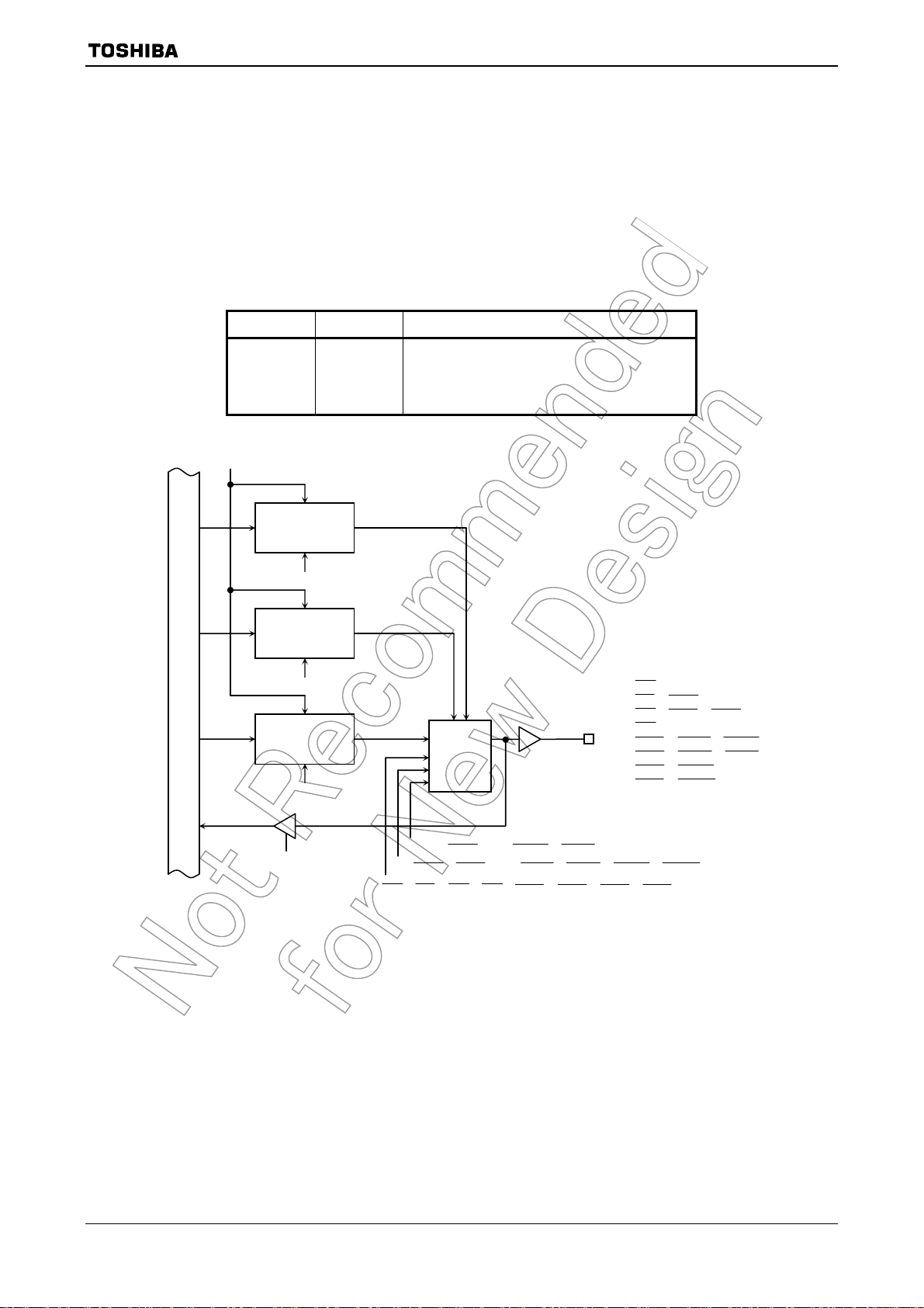
3.5.8 Port 8 (P80 to P87)
Ports 80 to 87 are 8-bit output ports. Resetting sets the output latch of P82 to “0” and the
output latches of P80 to P81, P83 to P87 to “1”.
Port 8 can also be set to function as an interface pin for external memory using function
register P8FC.
Writing “1” in the corresponding bit of P8FC and P8FC2 enables the respective functions.
Resetting <P80F> to <P87F> of P8FC to “0” and P8FC2 to “0”, sets all bits to output
ports.
AM1 AM0 Function Setting after Reset is Released
Reset
Internal data bus
Port 82 Initial State
0 0 Don’t use this setting
0 1 “0” Output port
1 0 “0” Output port
1 1 “1” Output port
Function
control 2
P8FC2 write
Function
contol
P8FC write
Ouptut latch
P8 write
Selector
P80 ( CS0 )
P81 (
CS1 , SDCS )
P82 (
CS2 , CSZA , SDCS )
P83 (
CS3 )
P84 (
CSZB , WRUL , CE0ND )
P85 (
CSZC , WRUU , CE1ND )
CSZD , SRULB )
P86 (
P87 (
CSZE , SRUUB )
TMP92CH21
P8 read
“1”, “1”, SDCS , “1”, CE0ND , CE1ND , “1”, “1”,
“1”, SDCS , CSZA , “1”, WRUL , WRUU , SRULB , SRUUB
CS0 , CS1 , CS2, CS3, CSZB , CSZC , CSZD , CSZE
Figure 3.5.16 Port 8
92CH21-82
2009-06-19

Register
Port 8
(0020H)
Reset State 1 1 1 1 1 0/1 Note2 1 1
7 6 5 4 3 2 1 0
Bit symbol P87 P86 P85 P84 P83 P82 P81 P80 P8
Read/Write R/W
TMP92CH21
Port 8 Function Register
(0023H)
Reset State 0 0 0 0 0 0 0 0
Function 0: Port
7 6 5 4 3 2 1 0
Bit symbol P87F P86F P85F P84F P83F P82F P81F P80F P8FC
Read/Write W
1:
CSZE
0:
1:
Port
CSZD
Refer to
following
table
Refer to
following
table
0:
1:
Port
Refer to
following
3CS
table
0:
1:
Port
1CS
0:
1:
Port
0CS
Port 8 Function Register 2
(0021H)
Reset State 0 0 0 0 0 0 0 0
Function 0: <P87F>
7 6 5 4 3 2 1 0
Bit symbol P87F2 P86F2 P85F2 P84F2 P83F2 P82F2 P81F2 P80F2 P8FC2
Read/Write W
1:
SRUUB
0: <P86F>
1: SRULB
Refer to
following
table
Refer to
following
table
Always write
“0”
Refer to
table below
0: <P81F>
1:
SDCS
Always write
“0”
Port 8 Drive Register
(0088H)
Reset State 1 1 1 1 1 1 1 1
Function Input/Output buffer drive register for standby mode
7 6 5 4 3 2 1 0
Bit symbol P87D P86D P85D P84D P83D P82D P81D P80D P8DR
Read/Write R/W
P85 Setting
<P85F>
<P85F2>
0 Output port CSZC output
1 WRUU output ND1CE output
0 1
Note 1: Read-modify-write is prohibited for P8FC and P8FC2.
Note 2: It is set to “0” or “1” by AM pin setting.
Note 3: In MULTI16 or MULTI32 mode, do not write “1” to P8<P82> register before setting P82 pin to
because, on reset, P82 pin outputs “0” as
P84 Setting
<P84F>
<P84F2>
0 Output port CSZB output
1 WRUL output ND0CE output
0 1
CE for program memory.
P82 Setting
<P82F>
<P82F2>
0 Output port 2CS output
1 CSZA output SDCS output
0 1
2CS or CSZA
Figure 3.5.17 Register for Port 8
92CH21-83
2009-06-19

3.5.9 Port 9 (P90 to P97)
P90 to P94 are 5-bit general-purpose I/O ports. I/O can be set on a bit basis using the
control register. Resetting sets P90 to P94 to input port and all bits of output latch to“1”.
P95 is 1-bit general-purpose output port and P96 to P97 are 2-bit general-purpose input
ports. P90 to P92 function as SIO or I
P96 to P97 as input pins for external interruption (INT4, INT5). In addition, P95 functions
as the output pin for a low frequency oscillator, P96 to P97 as PX and PY pins for a touch
screen interface.
Setting the corresponding bits of P9CR and P9FC enables the respective functions.
Resetting resets the P9FC to “0”, and sets all bits except P95 to input ports.
(1) Port 90 (TXD0, I2SCKO), Port91 (RXD0, I2SDO), Port 92 (SCLK0,
Ports 90 to 92 are general-purpose I/O ports. They also function as either SIO0 or I
Each pin is detailed below.
SIO mode
P90 TXD0
P91 RXD0
P92 SCLK0
Internal data bus
TXD0, I2SCKO output
(SIO0 module)
(Data output)
(Data input)
(Clock input or
output)
Reset
Direction control
P9CR write
Function control
P9FC write
S
Output latch
P9 write
P9 read
2
S, P93 to 95 as output pins for an LCD controller and
UART, IrDA mode
(SIO0 module)
TXD0
(Data output)
RXD0
(Data input)
A
Selector
B
Selector
0CTS
S
S
B
A
(Clear to send)
2
I
S mode
2
S module)
(I
I2SCKO
(Clock output)
I2SDO
(Data output)
I2SWS
(Word select
output)
Open-drain enable
P9FC2<P90F2>
TMP92CH21
CTS0 I2SWS)
SIO mode
(I2S module)
I2SCKO
(Clock output)
I2SDO
(Data output)
(No use)
P90 (TXD0, I2SCKO)
2
S.
Figure 3.5.18 P90
92CH21-84
2009-06-19

TMP92CH21
Reset
Direction control
P9CR write
Function control
Internal data bus
SCLK0,I2SWS output
P9FC write
S
Output latch
P9 write
I2SDO output
P9 read
S
A
Selector
B
S
B
Selector
A
(to Port F1) P91RXD0 input
(to Port F2) P92SCLK0 input
P91 (RXD0, I2SDO)
P92 (SCLK0,
0CTS , I2SWS)
Figure 3.5.19 P91 and P92
(2) P93 (LGOE0), P94 (LGOE1)
Reset
Direction control
P9CR write
Function control
Internal data bus
P9FC write
S
Output latch
P9 write
LGOE0, LGOE1
P9 read
S
A
Selector
B
S
Selector
P93(LGOE0),
P94(LGOE1)
B
A
Figure 3.5.20 Port 93 and 94
92CH21-85
2009-06-19

y
TMP92CH21
(3) P95 (CLK32KO, LGOE2)
Reset
Direction control
P9CR write
Function control
Internal data bus
P9FC write
Output latch
P9 write
LGOE2
fs
S
A
Selector
B
C
P95 (LGOE2, CLK32KO)
P9 read
Figure 3.5.21 Port 95
(4) P96 (INT4, PX), P97 (INT5, PY)
Reset
Internal data bus
Function control
P9FC write
TSICR0<PXEN>
<
TSICR0<TSI7>
AVCC
>
Switch for TSI
Typ.20
Ω
P9 read
TSICR1<DBC7>
P96 (INT4, PX)
P97 (INT5, PY)
Only for P96
INT4
INT5
Rising/Falling
edge detection
IIMC<I4EDGE,
I5EDGE>
S
A
Selector
B
TSICR0<TWIEN, TSI7>
TSICR0<PXEN>
TSICR0<TSI7>
De-bounce
circuit
Pull-down resistor
t
p.200kΩ
Figure 3.5.22 Port 96, 97
92CH21-86
2009-06-19

Register
Port 9
(0024H)
Reset State Data from external port 0 Data from external port (Output latch register is set to “1”)
7 6 5 4 3 2 1 0
Bit symbol P97 P96 P95 P94 P93 P92 P91 P90 P9
Read/Write R R/W
TMP92CH21
Port 9 Function Register
(0026H)
Reset State 0 0 0 0 0 0
Function Refer to following table
7 6 5 4 3 2 1 0
Bit symbol P95C P94C P93C P92C P91C P90C P9FC
Read/Write W
Port 9 Function Register
(0027H)
Reset State 0 0 0 0 0 0 0 0
Function 0: Input port
P92 Setting
<P92C>
<P92F>
0
1 I2SWS output SCLK0 output
P95 Setting
<P95C>
<P95F>
0 Output port CLK3 2KO output
1 LGOE2 output (Reserved)
7 6 5 4 3 2 1 0
Bit symbol P97F P96F P95F P94F P93F P92F P91F P90F P9FC
Read/Write W
1: INT5
0 1
Input port
SCLK0, 0CTS input
0 1
Output port
0: Input port
1: INT4
P91 Setting
<P91C>
<P91F>
P94 Setting
<P94C>
<P94F>
0 1
0
1 I2SDO output (Reserved)
0 Input port Output port
1 LGOE1 output (Reserved)
Input port
RXD0 input
0 1
Output port
Refer to following table
P90 Setting
<P90C>
<P90F>
0
1 I2SCKO output TXD0 output
P93 Setting
<P93C>
<P93F>
0 Input port Output port
1 LGOE0 output (Reserved)
0 1
Input port Output port
0 1
Port 9 Function Register 2
(0025H)
Reset State 0
Function 0:CMOS
7 6 5 4 3 2 1 0
Bit symbol P90F2 P9FC2
Read/Write W
1:Opendrain
Port 9 Drive Register
(0089H)
Reset State 1 1 1 1 1 1 1 1
Function Output/Input buffer drive register for standby mode
Note: Read-modify-write is prohibited for P9CR, P9FC and P9FC2.
7 6 5 4 3 2 1 0
Bit symbol P97D P96D P95D P94D P93D P92D P91D P90D P9DR
Read/Write R/W
Figure 3.5.23 Register for Port 9
92CH21-87
2009-06-19

3.5.10 Port A (PA0 to PA7)
Ports A0 to A7 are 8-bit input ports with pull-up resistor. In addition to functioning as
general-purpose I/O ports, ports A0 to A7 can also, as a keyboard interface, operate a
key-on wakeup function. The various functions can each be enabled by writing a “1” to the
corresponding bit of the port A function register (PAFC).
Resetting resets all bits of the register PAFC to “0” and sets all pins to be input port.
TMP92CH21
PAFC write
PA read
PACR write
PA0 to PA7
8-input OR
Reset
PAFC
Reset
PACR
LD8 to LD11
Pull-up resistor
PA0 (KI0)
PA1 (KI1)
PA2 (KI2)
PA3 (KI3, LD8)
PA4 (KI4, LD9)
PA5 (KI5, LD10)
PA6 (KI6, LD11)
PA7 (KI7)
Only for PA3 to PA6
INTKEY
Edge
detection
Internal data bus
Figure 3.5.24 Port A
When PAFC = “1”, if the input of any of KI0 to KI7 pins fall down, an INTKEY interrupt
is generated. An INTKEY interrupt can be used to release all HALT modes.
92CH21-88
2009-06-19

TMP92CH21
Port A Register
7 6 5 4 3 2 1 0
PA
(0028H)
Bit symbol PA7 PA6 PA5 PA4 PA3 PA2 PA1 PA0
Read/Write R/W
Reset State Data from external port
Port A Function Register
7 6 5 4 3 2 1 0
PAFC
(002BH)
Bit symbol PA7F PA6F PA5F PA4F PA3F PA2F PA1F PA0F
Read/Write W
Reset State 0 0 0 0 0 0 0 0
Function 0: Key input disable 1: Key input enable
Port A Control Register
7 6 5 4 3 2 1 0
PACR
(002AH)
Bit symbol PA6C PA5C PA4C PA3C
Read/Write W
Reset State 0 0 0 0
Function 0: Input port or Key input
1: LD11 to LD8 output
Port A Drive register
7 6 5 4 3 2 1 0
PADR
(008AH)
Bit symbol PA7D PA6D PA5D PA4D PA3D PA2D PA1D PA0D
Read/Write W
Reset State 1 1 1 1 1 1 1 1
Function Input/Output buffer drive register for standby mode
Note: Read-modify-write is prohibited for PACR and PAFC.
Figure 3.5.25 Register for Port A
92CH21-89
2009-06-19

3.5.11 Port C (PC0 to PC3, PC6 to PC7)
PC0 to PC3, PC6 and PC7 are 6-bit general-purpose I/O ports. Each bit can be set
individually for input or output. Resetting sets port C to an input port.
In addition to functioning as a general-purpose I/O port, port C can also function as an
output pin for timers (TA1OUT, TA3OUT and TB0OUT0), input pin for external
interruption (INT0 to INT3), output pin for memory (
output pin for LCD driver (LDIV, LCP1). These settings are made using the function
register PCFC. The edge select for external interruption is determined by the IIMC register
in the interruption controller.
(1) PC0 (INT0, TA1OUT)
Internal data bus
TA1OUT
Reset
Direction control
PCCR write
Function control
PCFC write
Output latch
PC write
PC read
INT0
TMP92CH21
CSZF
), output pin for key (KO8) and
S
S
A
Selector
B
S
B
Selector
A
Level/edge select
and
Rising/falling select
IIMC<I0LE, I0EDGE>
PC0 (INT0,
TA1OUT)
Figure 3.5.26 Port C0
92CH21-90
2009-06-19

(2) PC1 (INT1, TA3OUT), PC2 (INT2, TB0OUT0), PC3 (INT3, TB0OUT1)
TMP92CH21
Reset
Direction control
PCCR write
Function control
Internal data bus
PCFC write
S
Output latch
PC write
TA3OUT
TB0OUT0
PC read
INT1
to
INT3
S
A
Selector
B
S
B
Selector
A
Rising/falling
edge detection
PC1 (INT1, TA3OUT)
PC2 (INT2, TB0OUT0)
PC3 (INT3)
IIMC<I1EDGE,
I2EDGE,
I3EDGE >
Figure 3.5.27 Port C1, C2, C3
92CH21-91
2009-06-19

TMP92CH21
(3) PC6 (KO8, LDIV)
Reset
Direction control
PCCR write
Internal data bus
Figure 3.5.28 Port C6
Function control
PCFC write
S
Output latch
PC write
LDIV
PC read
S
A
Selector
B
S
Selector
PC6 (KO8, LDIV)
Open drain
possible
B
A
(4) PC7 (
CSZF , LCP1)
Reset
Direction control
PCCR write
Funtcion control
Internal data bus
S
Output latch
PC write
PC read
CSZF
LCP1
S
A
Selector
B
C
S
Selector
CSZF , LCP1)
PC7 (
B
A
Figure 3.5.29 Port C7
92CH21-92
2009-06-19

TMP92CH21
Port C Register
(0030H)
Reset State Data from external port
7 6 5 4 3 2 1 0
Bit symbol PC7 PC6 PC3 PC2 PC1 PC0 PC
Read/Write R/W R/W
Data from external port
(Output latch register is
set to “1”)
(Output latch register is set to “1”)
Port C Control Register
(0032H)
Reset State 0 0 0 0 0 0
Function Refer to following table Refer to following table
7 6 5 4 3 2 1 0
Bit symbol PC7C PC6C PC3C PC2C PC1C PC0C PCCR
Read/Write W W
Port C Function Register
(0033H)
Reset State 0 0 0 0 0 0
Function Refer to following table Refer to following table
PC2 Setting
<PC2C>
<PC2F>
0 Input port Output port
1 INT2 TB0OUT
PC7 Setting
<PC7C>
<PC7F>
0 Input port Output port
1 CSZF Output LCP1 Output
7 6 5 4 3 2 1 0
Bit symbol PC7F PC6F PC3F PC2F PC1F PC0F PCFC
Read/Write W W
PC1 Setting
0 1
0 1
<PC1F>
PC6 Setting
<PC6F>
<PC1C>
0 1
0 Input port Output port
1 INT1 TA3OUT
<PC6C>
0 1
0 Input port Output port
1
KO8
(Open drain)
LDIV Output
PC0 Setting
<PC0C>
<PC0F>
0 Input port Output port
1 INT0 TA1OUT
PC3 Setting
<PC3C>
<PC3F>
0 Input port Output port
1 INT3 (Reserved)
0 1
0 1
Port C Drive Register
PCDR
(008CH)
7 6 5 4 3 2 1 0
Bit symbol PC7D PC6D PC3D PC2D PC1D PC0D
Read/Write R/W R/W
Reset State 1 1 1 1 1 1
Function Input/Output buffer drive
register for standby mode
Note: Read-modify-write is prohibited for the registers PCCR and PCFC.
Input/Output buffer drive register for standby mode
Figure 3.5.30 Register for Port C
92CH21-93
2009-06-19

3.5.12 Port F (PF0 to PF2, PF7)
Ports F0 to F2 are 3-bit general-purpose I/O ports. Each bit can be set individually for
input or output. Resetting sets PF0 to PF2 to be input ports. It also sets all bits of the
output latch register to “1”. In addition to functioning as general-purpose I/O port pins, PF0
to PF2 can also function as the I/O for serial channels 0 and 1. A pin can be enabled for I/O
by writing a “1” to the corresponding bit of the port F function register (PFFC).
Port F7 is a 1-bit general-purpose output port. In addition to functioning as a
general-purpose output port , PF7 can also function as the SDCLK output. Resetting sets
PF7 to be an SDCLK output port.
(1) Port F0 (TXD0, TXD1), F1 (RXD0, RXD1), F2 (SCLK0,
Ports F0 to F2 are general-purpose I/O ports. They also function as either SIO0 or
SIO1. Each pin is detailed below.
SIO mode
(SIO0 module)
PF0
PF1
PF2
(Data output)
(Clock input or output)
TXD0
RXD0
(Data input)
SCLK0
UART, IrDA mode
(SIO0 module)
TXD0
(Data output)
RXD0
(Data input)
0CTS
(Clear to send)
CTS0 SCLK1,CTS1 )
SIO mode
(SIO1 module)
TXD1
(Data output)
RXD1
(Data input)
SCLK1
(Clock input or output)
TMP92CH21
UART mode
(SIO1 module)
TXD1
(Data output)
RXD1
(Data input)
1CTS
(Clear to send)
Reset
Direction control
PFCR write
Function control
Internal data bus
PFFC write
S
Output latch
PF write
TXD0
TXD1
PF read
S
Selector
S
Selector
PF0 (TXD0, TXD1)
Open drain
set possible
PFFC2<PF0F2>
B
A
Figure 3.5.31 Port F0
92CH21-94
2009-06-19

TMP92CH21
Reset
Direction control
Internal data bus
PFCR write
S
Output latch
PF write
PF read
RXD0
RXD1
Selector
PFFC<PF1F>
S
A
Selector
B
PF1 (RXD0,RXD1)
S
B
A
P91RXD0 input
Figure 3.5.32 Port F1
Reset
Direction control
Internal data bus
PFCR write
S
Output latch
PF write
Function control
SCLK0 output
SCLK1 output
Selector
S
PF2 (SCLK0,
SCLK1,
0CTS ,
1CTS )
SCLK0 input, 0CTS input
SCLK1 input,
PFFC write
PF read
1CTS input
S
Selector
S
B
Selector
A
A
B
P92SCLK0 input
Figure 3.5.33 Port F2
92CH21-95
2009-06-19

Reset
Function control
PFFC write
Internal data bus
S
Output latch
PF write
PF read
SDCLK
S
A
Selector
B
PF7 (SDCLK)
TMP92CH21
Figure 3.5.34 Port F7
92CH21-96
2009-06-19
TMP92CH21
Port F Register
(003CH)
Reset State
7 6 5 4 3 2 1 0
Bit symbol PF7 PF2 PF1 PF0 PF
Read/Write R/W R/W
1
External data
(Output latch register is set to “1”)
Port F Control Register
(003EH)
Reset State 0 0 0
Function Refer to following table
7 6 5 4 3 2 1 0
Bit symbol PF2C PF1C PF0C PFCR
Read/Write W
Port F Functon Register
(003FH)
Reset State 1 0 0 0
Function 0: Output
7 6 5 4 3 2 1 0
Bit symbol PF7F PF2F PF1F PF0F PFFC
Read/Write W W
Refer to
following
table
1: SDCLK
Refer to
following
table
RXD0 pin
selection
0: Port F1
1: Port 91
PF2 Setting
<PF2C>
<PF2F>
Input port or
SCLK1, 1CTS input or
0
SCLK0, 0CTS input
From PF2 pin at <PF2> = 0
From P92 pin at <PF2> = 1
1 SCLK1 output
0 1
Output
port
SCLK0
output
PF1 Setting
<PF1C>
<PF1F>
0
1
0 1
Input port or
RXD0/RXD1 input
Output
port
PF0 Setting
<PF0C>
<PF0F>
0 Input port Output port
1 TXD1 output TXD0 output
0 1
Port F Functon Register 2
(003DH)
Reset State 0
Function Output buffer
7 6 5 4 3 2 1 0
Bit symbol PF0F2 PFFC2
Read/Write W
0: CMOS
1: Open drain
Port F Drive Register
PFDR
(008FH)
7 6 5 4 3 2 1 0
Bit symbol PF7D PF2D PF1D PF0D
Read/Write R/W R/W
Reset State 1 1 1 1
Function Input/Output
buffer drive
register for
standby
mode
Note: Read-modify-write is prohibited for the registers PFCR, PFFC and PFFC2.
Input/Output buffer drive register for
standby mode
Figure 3.5.35 Register for Port F
92CH21-97
2009-06-19

3.5.13 Port G (PG0 to PG3)
PG0 to PG3 are 4-bit input ports and can also be used as the analog input pins for the
internal AD converter. PG3 can also be used as the ADTRG pin for the AD converter.
PG2 and PG3 can also be used as the MX and MY pins for a touch screen interface.
TMP92CH21
Internal data bus
Port G read
AD read
Conversion
result
register
AD
converter
Channel
selector
PG0 (AN0),
PG1 (AN1),
PG2 (AN2, MX),
PG3 (AN3, MY,
ADTRG )
ADTRG
(only for PG3)
(Only for PG2, PG3)
TSICR0<MXEN, MYEN>
Switch for TSI
Ω
typ. 20
TSICR0<TSI7>
Figure 3.5.36 Port G
Port G Register
(0040H)
Reset State Data from external port
7 6 5 4 3 2 1 0
Bit symbol PG2 PG2 PG1 PG0 PG
Read/Write R
Note: The input channel selection of the AD converter and the permission for ADTRG input are set by AD converter mode
register ADMOD1.
Port G Drive Register
(0090H)
Reset State 1 1
Function Input/Output buffer drive
7 6 5 4 3 2 1 0
Bit symbol PG3D PG2D PGDR
Read/Write R/W
register for standby mode
Figure 3.5.37 Register for Port G
92CH21-98
2009-06-19
 Loading...