


TOSHIBA Original CMOS 16-Bit Microcontroller
TLCS-900/L1 Series
TMP91FY42FG
Semiconductor Company

Preface
Thank you very much for making use of Toshiba microcomputer LSIs.
Before use this LSI, refer the section, “Points of Note and Restrictions”.
Especially, take care below cautions.

1. Outline and Features
TMP91FY42F is a high-speed 16-bit microcontroller designed for the control of various mid- to
large-scale equipment.
TMP91FY42FG comes in a 100-pin flat package.
Listed below are the features.
(1) High-speed 16-bit CPU (900/L1 CPU)
• Instruction mnemonics are upward-compatible with TLCS-90/900
• General-purpose registers and register banks
• 16 Mbytes of linear address space
• 16-bit multiplication and division instructions; bit transfer and arithmetic instructions
• Micro DMA: 4-channels (593 ns/2 bytes at 27 MHz)
(2) Minimum instruction execution time: 148 ns (at 27 MHz)
TMP91FY42
CMOS 16-Bit Microcontrollers
TMP91FY42FG
RESTRICTIONS ON PRODUCT USE
• The information contained herein is subject to change without notice. 021023_D
• TOSHIBA is continually working to improve the quality and reliabil ity of its products. Nevertheless, semiconductor
devices in general can malfunction or fail due to their inherent electrical sensitivity an d vulnerability to physical
stress. It is the responsibility of the buyer, when utilizing TOSHIBA products, to comply with the standards of safety
in making a safe design for the entire system, and to avoid situations in which a malfunction or failure of such
TOSHIBA products could cause loss of human life, bodily injury or damage to property.
In developing your designs, please ensure that TOSHIBA products are used within specified operating ranges as
set forth in the most recent TOSHIBA products specifications. Also, please keep in mind the precautions and
conditions set forth in the “Handling Guide for Semiconductor Devices,” or “TOSHIBA Semiconductor Reliability
Handbook” etc.
• The TOSHIBA products listed in this document are intended for usage in general electronics applications (computer,
personal equipment, office equipment, measuring equipment, industrial robotics, domestic appliances, etc.). These
TOSHIBA products are neither intended nor warranted for usage in equipment that requires extraordinarily high
quality and/or reliability or a malfunction or failure of which may cause loss of human life or bodily injury
(“Unintended Usage”). Unintended Usage include atomic energy control instruments, airplane or spaceship
instruments, transportation instruments, traffic signal instruments, combustion control instruments, medical
instruments, all types of safety devices, etc. Unintended Usage of TOSHIBA products listed in this document shall
be made at the customer’s own risk.
• The products described in this document shall not be used or embedded to any downstream products of which
manufacture, use and/or sale are prohibited under any applicable laws and regulations. 060106_Q
021023_A
021023_B
060925EBP
• The information contained herein is presented only as a guide for the applications of our products. No responsibility
is assumed by TOSHIBA for any infringements of patents or other rights of the third parties which may result from its
use. No license is granted by implication or otherwise under an y patent or patent rights of TOSHIBA or others.
021023_C
• The products described in this document are subject to foreign exchange and foreign trade control laws. 060925_E
• For a discussion of how the reliability of microcontrollers can be predicted, please refer to Section 1.3 of the chapter
entitled Quality and Reliability Assurance/Handling Precautions. 030619_S
This product uses the Super Flash® technology under the license of Silicon Storage Technology,Inc.
Super Flash® is a registered trademark of Silicon Storage Technology,Inc.
91FY42-1 2006-11-08

TMP91FY42
(3) Built-in RAM: 16 Kbytes
Built-in ROM: 256 Kbytes Flash memory
4 Kbytes mask ROM (used for booting)
(4) External memory expansion
• Expandable up to 16 Mbytes (shared program/data area)
• Can simultaneously support 8-/16-bit width external data bus
… Dynamic data bus sizing
(5) 8-bit timers: 8 channels
(6) 16-bit timer/event counter: 2 channels
(7) General-purpose serial interface: 2 channels
• UART/ Synchronous mode: 2 channels
• IrDA ver1.0 (115.2 kbps) supported: 1 channel
(8) Serial bus interface: 1 channel
2
C bus mode/clock synchronous Select mode
• I
(9) 10-bit AD converter (built-in sample hold circuit) : 8 channels
(10) Watchdog timer
(11) Special timer for clock
(12) Chip Select/Wait controller: 4 channels
(13) Interrupts: 45 interrupts
• 9 CPU interrupts: Software interrupt instruction and illegal instruction
• 26 internal interrupts:
Seven selectable priority levels
• 10 external interrupts:
(14) Input/Output ports: 81 pins
(15) Standby function
Three HALT modes: IDLE2 (programmable), IDLE1, STOP
(16) Clock controller
• Clock Gear function: Select a high-frequency clock (fc to fc/16)
• Special timer for CLOCK (fs = 32.768 kHz)
(17) Operating voltage
• V
• V
= 2.7 V to 3.6 V (fc max = 27 MHz, flash memory read operation)
CC
= 3.0 V to 3.6 V (fc max = 27 MHz, flash memory erase/program operations)
CC
(18) Package
• 100-pin LQFP: LQFP100-P-1414-0.50F
Note: This LSI does not build in Clock doubler (DFM.)
91FY42-2 2006-11-08
(
(
(
TMP91FY42
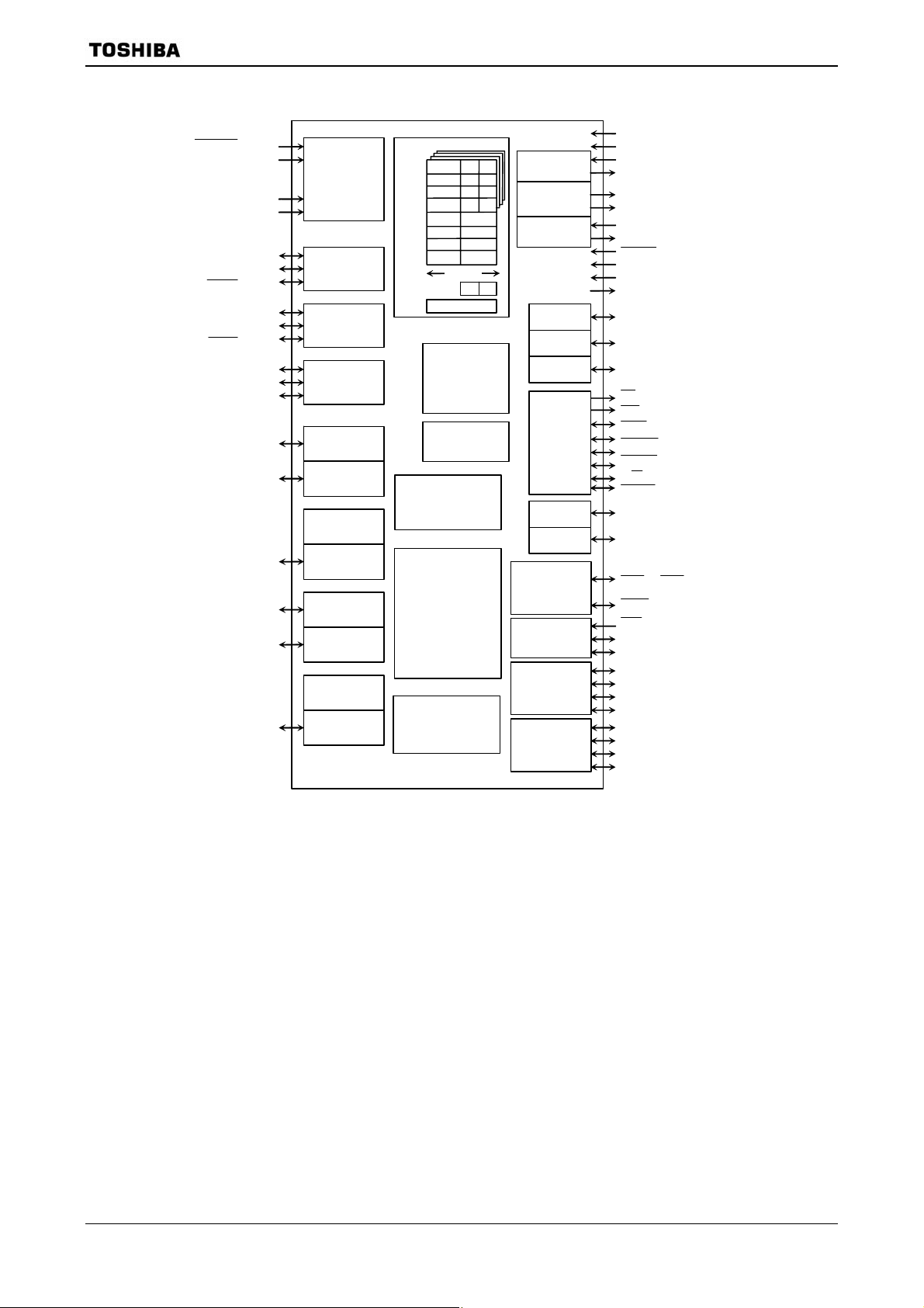
ADTRG (P53)
(P50 to P57)
AVCC, AVSS
VREFH, VREFL
RXD0 (P91)
SCLK0/
RXD1 (P94)
SCLK1/
CTS1 (P95)
SO/SDA (P61)
SI / SCL (P62)
TA0IN (P70)
TA1OUT (P71)
TA3OUT (P72)
TA4IN (P73)
TA5OUT (P74)
TA7OUT (P75)
AN0 to AN7
TXD0 (P90)
0CTS (P92)
TXD1 (P93)
SCK (P60)
10-Bit 8CH
AD
Converter
SIO/UART/IrDA
(SIO0)
SIO/UART
(SIO1)
Serial Bus
Interface
SBI)
8-Bit Timer
(TMRA0)
8-Bit Timer
(TMRA1)
8-Bit Timer
(TMRA2)
8-Bit Timer
(TMRA3)
8-Bit Timer
(TMRA4)
8-Bit Timer
(TMRA5)
8-Bit Timer
(TMRA6)
8-Bit Timer
(TMRA7)
CPU (TLCS-900/L1)
XWA
XBC
XDE
XHL
XIX
XIY
XIZ
XSP
16-KB RAM
W A
B C
D E
H L
IX
IY
IZ
SP
32 bits
PC
Watchdog
Timer (WDT)
Special timer
for CLOCK
256-KB FLASH
2
PROM
E
4-KB BOOT ROM
FSR
H-OSC
Clock Gear
Clock doubler
L-OSC
Port 0
Port 1
Port 2
Port 3
Port 6
Port A
CS/WAIT
Controller
(4-BLOCK)
Interrupt
Controller
16-Bit Timer
(TMRB0)
16-Bit Timer
(TMRB1)
DVCC [3]
DVSS [3]
X1
X2
EMU0
EMU1
XT1 (P96)
XT2 (P97)
RESET
AM0
AM1
ALE
(P00 to P07)
AD0 to AD7
(P10 to P17)
AD8/A8 to AD15/A15
(P20 to P27)
A0/A16 to A7/A23
RD (P30)
WR (P31)
HWR (P32)
BUSRQ (P34)
BUSAK (P35)
WR/ (P36)
BOOT
SCOUT(P64), P65, P66
PA4 to PA7
(P40 to P43)
CS0 to CS3
WAIT
NMI
INT0 (P64)
INT1 to INT4
(PA0 to PA3)
TB0IN0/INT5 (P80)
TB0IN1/INT6 (P81)
TB0OUT0 (P82)
TB0OUT1 (P83)
TB1IN0/INT7 (P84)
TB1IN1/INT8 (P85)
TB1OUT0 (P86)
TB1OUT1 (P87)
P37)
P33)
( ): Initial function after reset
Figure 1.1 TMP91FY42F Block Diagram
91FY42-3 2006-11-08
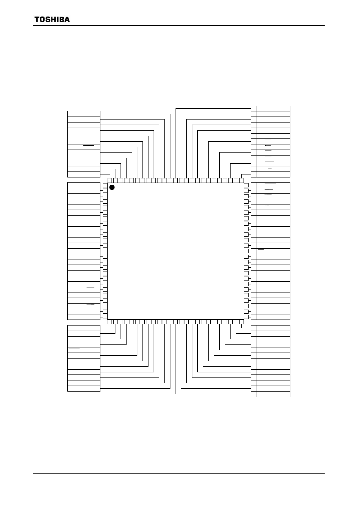
2. Pin Assignment and Pin Functions
The assignment of input/output pins for the TMP91FY42, their names and functions are as
follows:
2.1 Pin Assignment Diagram
Figure 2.1.1 shows the pin assignment of the TMP91FY42.
DVCC 89
P66 90
DVSS 91
P50/AN0 92
P51/AN1 93
P52/AN2 94
P53/AN3/ADTRG 95
P54/AN4 96
P55/AN5 97
P56/AN6 98
P57/AN7 99
VREFH 100
VREFL 1
AVSS 2
AVCC 3
P70/TA0IN 4
P71/TA1OUT 5
P72/TA3OUT 6
P73/TA4IN 7
P74/TA5OUT 8
P75/TA7OUT 9
P80/TB0IN0/INT5 10
P81/TB0IN1/INT6 11
P82/TB0OUT0 12
P83/TB0OUT1 13
P84/TB1IN0/INT7 14
P85/TB1IN1/INT8 15
P86/TB1OUT0 16
P87/TB1OUT1 17
P90/TXD0 18
P91/RXD0 19
P92/SCLK0/CTS0 20
P93/TXD1 21
P94/RXD1 22
P95/SCLK1/CTS1 23
AM0 24
DVCC 25
X2 26
DVSS 27
X1 28
AM1 29
RESET 30
P96/XT1 31
P97/XT2 32
EMU0 33
EMU1 34
PA0/INT1 35
PA1/INT2 36
PA2/INT3 37
Top view
QFP100
TMP91FY42
88 P65
87 P64/SCOUT
86 P63/INT0
85 P62/SI/SCL
84 P61/SO/SDA
83 P60/SCK
82 P43/CS3
81 P42/CS2
80 P41/CS1
79 P40/CS0
78 P37/BOOT
77 P36/R/W
76 P35/BUSAK
75 P34/BUSRQ
74 P33/WAIT
73 P32/HWR
72 P31/WR
71 P30/RD
70 P27/A7/A23
69 P26/A6/A22
68 P25/A5/A21
67 P24/A4/A20
66 P23/A3/A19
65 P22/A2/A18
64 DVCC
63 NMI
62 DVSS
61 P21/A1/A17
60 P20/A0/A16
59 P17/AD15/A15
58 P16/AD14/A14
57 P15/AD13/A13
56 P14/AD12/A12
55 P13/AD11/A11
54 P12/AD10/A10
53 P11/AD9/A9
52 P10/AD8/A8
51 P07/AD7
50 P06/AD6
49 P05/AD5
48 P04/AD4
47 P03/AD3
46 P02/AD2
45 P01/AD1
44 P00/AD0
43 ALE
42 PA7
41 PA6
40 PA5
39 PA4
38 PA3/INT4
Figure 2.1.1 Pin assignment diagram (100-pin LQFP)
91FY42-4 2006-11-08

TMP91FY42
2.2 Pin Names and Functions
The names of the input/output pins and their functions are described below.
Table 2.2.1 Pin names and functions.
Table 2.2.1 Pin names and functions (1/3)
Pin Name
P00∼P07
AD0∼AD7
P10∼P17
AD8∼AD15
A8∼A15
P20∼P27
A0∼A7
A16∼A23
P30
RD
P31
WR
P32
HWR
P33
WAIT
P34
BUSRQ
P35
BUSAK
P36
W/R
P37
BOOT
P40
CS0
P41
CS1
P42
CS2
P43
CS3
P50∼P57
∼AN7
AN0
ADTRG
Number
of Pins
8 I/O
8 I/O
8 I/O
1 Output
1 Output
1 I/O
1 I/O
1 I/O
1 I/O
1 I/O
1 I/O
1 I/O
1 I/O
1 I/O
1 I/O
8 Input
I/O Functions
Port 0: I/O port that allows I/O to be selected at the bit level
I/O
Address and data (lower): Bits 0 to 7 of address and data bus
Port 1: I/O port that allows I/O to be selected at the bit level
I/O
Address and data (upper): Bits 8 to 15 for address and data bus
Output
Output
Output
Output
Output
Output
Output
Output
Output
Output
Output
Output
Address: Bits 8 to 15 of address bus
Port 2: I/O port that allows I/O to be selected at the bit level
Address: Bits 0 to 7 of address bus
Address: Bits 16 to 23 of address bus
Port 30: Output port
Read: Strobe signal for reading external memory
This port output RD signal also case of reading internal-area by setting P3
<P30> = 0 and P3FC <P30F> = 1.
Port 31: Output port
Write: Strobe signal for writing data to pins AD0 to AD7
Port 32: I/O port (with pull-up resistor)
High Write: Strobe signal for writing data to pins AD8 to AD15
Port 33: I/O port (with pull-up resistor)
Input
Wait: Pin used to request CPU bus wait
((1+N) WAIT mode)
Port 34: I/O port (with pull-up resistor)
Input
Bus Request: Signal used to request Bus Release
Port 35: I/O port (with pull-up resistor)
Bus Acknowledge: Signal used to acknowledge Bus Release
Port 36: I/O port (with pull-up resistor)
Read/Write: 1 represents Read or Dummy cycle; 0 represents Write cycle.
Port 36: I/O port (with pull-up resistor)
Input
This pin sets single boot mode.
When released reset, Single boot mode is started at P37
Port 40: I/O port (with pull-up resistor)
Chip Select 0: Outputs 0 when address is within specified address area
Port 41: I/O port (with pull-up resistor)
Chip Select 1: Outputs 0 if address is within specified address area
Port 42: I/O port (with pull-up resistor)
Chip Select 2: Outputs 0 if address is within specified address area
Port 43: I/O port (with pull-up resistor)
Chip Select 3: Outputs 0 if address is within specified address area
Port 5: Pin used to input port
Input
Analog input: Pin used to input to AD converter
Input
AD Trigger: Signal used to request start of AD converter (Shared with53 pin)
=Low level.
91FY42-5 2006-11-08

TMP91FY42
Table 2.2.1 Pin names and functions (2/3)
Pin Name
P60
SCK
P61
SO
SDA
P62
SI
SCL
P63
INT0
P64
SCOUT
P65 1 I/O Port 65 I/O port
P66 1 I/O Port 66 I/O port
P70
TA0IN
P71
TA1OUT
P72
TA3OUT
P73
TA4IN
P74
TA5OUT
P75
TA7OUT
P80
TB0IN0
INT5
P81
TB0IN1
INT6
P82
TB0OUT0
P83
TB0OUT1
P84
TB1IN0
INT7
P85
TB1IN1
INT8
P86
TB1OUT0
P87
TB1OUT1
Number
of Pins
1 I/O
1 I/O
1 I/O
1 I/O
1 I/O
1 I/O
1 I/O
1 I/O
1 I/O
1 I/O
1 I/O
1 I/O
1 I/O
1 I/O
1 I/O
1 I/O
1 I/O
1 I/O
1 I/O
I/O Functions
Port 60: I/O port
I/O
Serial bus interface clock in SIO Mode
Port 61: I/O port
Output
Output
Output
Output
Output
Output
Output
Output
Output
Output
Serial bus interface send data at SIO mode
I/O
Serial bus interface send/recive data at I
Open-drain output mode by programmable
Port 62: I/O port
Input
Serial bus interface recive data at SIO mode
I/O
Serial bus interface clock I/O data at I
Open-drain output mode by programmable
Port 63: I/O port
Input
Interrupt Request Pin 0: Interrupt request pin with
rising edge / falling edge
Port 64: I/O port
System Clock Output: Outputs f
Port 70I/O port
Input
8bitt timer 0 input:: Timer 0 input
Port 71I/O port
8-bit timer 1 output: Timer 0 or Timer 1 output
Port 72I/O port 8bit
8-bit timer 3 output: Timer 2 or Timer 3 output
Port 73: I/O port
Input
8-bit timer 4 input: Timer 4 input
Port 74: I/O port
8-bit timer 5 output: Timer 4 or Timer 5 output
Port 75: I/O port
88-bit timer 7 output: Timer 6 or Timer 7 output
Port 80: I/O port
Input
16bit timer 0 input 0: 16bit Timer 0 count / capture trigger input
Input
Interrupt Request Pin 5: Interrupt request pin with programmable rising edge
/ falling edge.
Port 81: I/O port
Input
16bit timer 0 input 1: 16bit Timer 0 count / capture trigger input
Input
Interrupt Request Pin 6: Interrupt request on rising edge
Port 82: I/O port
16bit timer 0 output 0: 16bit Timer 0 output
Port 83: I/O port
16bit timer 0 output 1: 16bit Timer 0 output
Port 84: I/O port
Input
16bit timer 1 input 0: 16bit Timer 1 count / capture trigger input
Input
Interrupt Request Pin 7: Interrupt request pin with programmable rising edge
/ falling edge.
Port 85: I/O port
Input
16bit timer 1 input 1: 16bit Timer 1 count / capture trigger input
Input
Interrupt Request Pin 8: Interrupt request on rising edge
Port 86: I/O port
16bit timer 1 output 0: 16bit Timer 1 output 16bit
Port 87: I/O port
16bit timer 1 output 1: 16bit Timer 1 output 16bit 16bit
2
or fs clock.
FPH
2
C bus mode
C bus mode
programmable level /
91FY42-6 2006-11-08

TMP91FY42
Table 2.2.1 Pin names and functions (3/3)
Pin Name
P90
TXD0
P91
RXD0
P92
SCLK0
0CTS
P93
TXD1
P94
RXD1
P95
SCLK1
CTS1
P96
XT1
P97
XT2
PA0∼PA3
INT1
∼INT4
PA4∼PA7 4 I/O Ports A4 to A7: I/O ports
ALE 1 Output Address Latch Enable
NMI
AM0∼1
EMU0 1 Output Open pin
EMU1 1 Output Open pin
RESET
VREFH 1 Input Pin for reference voltage input to AD converter (H)
VREFL 1 Input Pin for reference voltage input to AD converter (L)
AVCC 1 Power supply pin for AD converter
AVSS 1 GND pin for AD converter (0 V)
X1/X2 2 I/O High-frequency oscillator connection pins
DVCC 3 Power supply pins (All DVCC pins should be connected with the power supply pin.)
DVSS 3 GND pins (0 V) (All DVSS pins should be connected with the power supply pin.)
Number
of Pins
1 I/O
1 I/O
1 I/O
1 I/O
1 I/O
1 I/O
1 I/O
1 I/O
4 I/O
1 Input Non-Maskable Interrupt Request Pin: Interrupt request pin with programmable
2 Input
1 Input Reset: initializes TMP91FY42. (With pull-up resistor)
I/O Functions
Port 90: I/O port
Output
Output
Output
Serial Send Data 0 (programmable open-drain)
Port 91: I/O port
Input
Serial Receive Data 0
Port 92: I/O port
I/O
Serial Clock I/O 0
Input
Serial Data Send Enable 0 (Clear to Send)
Port 93: I/O port
Serial Send Data 1 (programmable open-drain)
Port 94: I/O port (with pull-up resistor)
Input
Serial Receive Data 1
Port 95: I/O port (with pull-up resistor)
I/O
Serial Clock I/O 1
Input
Serial Data Send Enable 1 (Clear to Send)
Port 96: I/O port (open-drain output)
Input
Low-frequency oscillator connection pin
Port 97: I/O port (open-drain output)
Low-frequency oscillator connection pin
Ports A0 to A3: I/O ports
Input
Interrupt Request Pins 1 to 4: Interrupt request pins with programmable rising
edge / falling edge.
Can be disabled to reduce noise.
falling edge or both edge.
Operation mode:
Fixed to AM1
= 1, AM0 = 1
Note: An external DMA controller cann ot access the device’s built-in memory or built-in I/O devices using
the
BUSRQ
and
BUSAK
signal.
91FY42-7 2006-11-08

3. Operation
This following describes block by block the functions and operation of the TMP91FY42.
Notes and restrictions for eatch book are outlined in 7 “Points of Note and Restrictions” at the
end of this manual.
3.1 CPU
The TMP91FY42 incorporates a high-performance 16-bit CPU (The 900/L1 CPU). For CPU
operation, see the “TLCS-900/L1 CPU”.
The following describe the unique function of the CPU used in the TMP91FY42; these
functions are not covered in the TLCS-900/L1 CPU section.
3.1.1 Reset
When resetting the TMP91FY42 microcontroller, ensure that the power supply voltage is
within the operating voltage range, and that the internal high-frequency oscillator has
stabilized. Then hold the
27MHz).
Thus, when turn on the switch, be set to the power supply voltage is within the operating
voltage range, and that the internal high-frequency oscillator has stabilized. Then hold the
RESET input to low level at least for 10 system clocks.
Clock gear is initialized 1/16 mode by reset operation. It means that the system clock
mode f
SYS
When the reset is accept, the CPU:
• Sets as follows the program counter (PC) in accordance with the reset vector stored
at address FFFF00H to FFFF02H:
TMP91FY42
RESET
is set to fc/32 (= fc/16 × 1/2).
PC<7:0> ← Value at FFFF00H address
input to low level for at least 10 system clocks (12μs at
PC<15:8> ← Value at FFFF01H address
PC<23:16> ← Value at FFFF02H address
• Sets the stack pointer (XSP) to 100H.
• Sets bits <IFF2:0> of the status register (SR) to 111 (Sets the interrupt level mark
register to level 7).
• Sets the <MAX> bit of the status register to 1 (MAX mode).
(Note: As this product does not support MIN mode, do not write a 0 to the <MAX>.)
• Clears bits <RFP2:0> of the status register to 000 (Sets the register bank to 0).
When reset is released,the CPU starts executing instructions in accordance with the
program counter settings. CPU internal registers not mentioned above do not change
when the reset is released.
When the reset is accepted, the CPU sets internal I/O, ports, and other pins as
follows.
• Initializes the internal I/O registers.
• Sets the port pins, including the pins that also act as internal I/O, to
general-purpose input or output port mode.
• Sets ALE pin to “High-Z"
Note: The CPU internal register (except to PC, SR, XSP) and internal RAM data do not
change by resetting.
Figure 3.1.1 is a reset timing of the TMP91FY42.
91FY42-8 2006-11-08

TMP91FY42
Read
(After reset is released, startting 0
wait read cycle)
Write
Sampling
(P32 imput mode)
(P20~P27 imput mode)
(P40~P43 imput mode)
Sampling
FPH
f
RESET
A16~A23
(P36 imput mode)
R/W
CS0∼CS3
(P00~P07, P10~P17 imput mode)
(P30 output mode)
Address
Address
ALE
AD0~AD15
RD
(P00~P07, P10~P17 imput mode)
Address
Data-out
Address
AD0~AD15
(P31 output mode)
WR
(Output mode)
(Imput mode)
(Imput mode)
: Pull-up (Internal)
: High-Z
HWR
P30∼P31
P32~P37, P40~P43
P00~P07, P10~P17,
P20~P27, P60~P66,
P70~P75, P80~P87,
P90~P97, PA0~PA7
Figure 3.1.1 TMP91FY42 Reset Timing Example
91FY42-9 2006-11-08

3.1.2 Outline of Operation Modes
There are single-chip and single-boot modes. Which mode is selected depends on the device’s
pin state after a reset.
• Single-chip mode: The device normally operations in this mode. After a reset, the device starts
executing the internal memory program.
• Single-boot mode: This mode is used to rewrite the internal flash memory by serial transfer
(UART).
After a reset, internal boot program starts up, executing an on-board rewrite
program.
Table 3.1.1 Operation Mode Setup Table
TMP91FY42
Operation Mode
Mode Setup Input Pin
RESET BOOT (P37)
Single-chip mode H
Single-boot mode
L
AM0 AM1
H H
91FY42-10 2006-11-08

3.2 Memory Map
Figure 3.2.1 is a memory map of the TMP91FY42.
000000H
000100H
Internal I/O
(4 Kbytes)
TMP91FY42
Direct area
(n)
001000H
005000H
010000H
FC0000H
Internal R A M
(16 Kbyte)
External memory
256 Kbyte
Internal ROM
64 Kbyte area
(nn)
16 Mbyte area
(R)
(−R)
(R+)
(R + R8/16)
(R + d8/16)
(nnn)
FFFF00H
FFFFFFH
Vector table (256 byte)
( = Internal area)
Figure 3.2.1 Memory Map
91FY42-11 2006-11-08

3.3 Triple Clock Function and Standby Function
TMP91FY42 contains (1) Clock gear, (2) Standby controller, and (3) Noise-reducing circuit. It
is used for low-power, low-noise systems.
This chapter is organized as follows:
• 3.3.1 Block Diagram of System Clock
• 3.3.2 SFRs
• 3.3.3 System Clock Controller
• 3.3.4 Prescaler Clock Controller
• 3.3.5 Noise Reduction Circuits
• 3.3.6 Standby Controller
TMP91FY42
91FY42-12 2006-11-08
TMP91FY42
The clock operating modes are as follows: (a) Single clock mode (X1, X2 pins only), (b) Dual
clock mode (X1, X2, XT1 and XT2 pins).
Figure 3.3.1 shows a transition figure.
IDLE2 mode
(I/O operate)
IDLE1 mode
(Operate only oscillator)
IDLE2 mode
(I/O operate)
IDLE1 mode
(Operate only oscillator)
IDLE2 mode
(I/O operate)
IDLE1 mode
(Operate only oscillator)
Instruction
Interrupt
Instruction
Interrupt
(a) Single clock mode transition figure
Instruction
Interrupt
Instruction
Interrupt
Instruction
Interrupt
Instruction
Interrupt
(b) Dual clock mode transition fiigure
Reset
/32)
(f
OSCH
Release reset
NORMAL mode
/gear value/2)
(f
OSCH
Reset
/32)
(f
OSCH
Release reset
NORMAL mode
/gear value/2)
(f
OSCH
SLOW mode
(fs/2)
Instruction
Instruction
Interrupt
Instruction
Interrupt
STOP mode
(Stops all circuits)
STOP mode
(Stops all circuits)
Figure 3.3.1 System Clock Block Diagram
The clock frequency input from the X1 and X2 pins is called fc and the clock frequency input
from the XT1 and XT2 pins is called fs. The clock frequency selected by SYSCR1<SYSCK> is
called the system clock f
one cycle of f
is defined to as one state.
SYS
. The system clock f
FPH
is defined as the divided clock of f
SYS
FPH
, and
TMP91FY42 does not built-in Clock Doubler (DFM).
91FY42-13 2006-11-08

3.3.1 Block Diagram of System Clock
SYSCR0<WUEF>
SYSCR2<WUPTM1:0>
Warm-up timer (High-/low-frequencyoscillator)
SYSCR0
<XTEN, RXTEN>
f
OSCH
fs
XT1
XT2
X1
X2
Low-frequency
oscillator
SYSCR0
<XEN, RXEN>
High-frequency
oscillator
fc
fc/2
÷2 ÷16 ÷4 ÷8
Clock gear
TMP91FY42
SYSCR0
<PRCK1:0>
fc/4
fc/8
fc/16
SYSCR1<GEAR2:0>
fc/16
f
FPH
SYSCR1<SYSCK>
÷2 ÷4
÷2
φT
φT0
fs
f
FPH
f
SYS
f
SYS
φT0
f
FPH
φT
TMRA01 toTMRA67
Prescaler
TMRB0 to TMRB1
Prescaler
SIO0~SIO1
Prescaler
SBI
Prescaler
Special timer for CLOCK
fs
Binary counter
SYSCR2<SCOSEL>
CPU
ROM
RAM
Interrupt
controller
CS/WAIT
controller
ADC
WDT
I/O ports
SCOUT
Figure 3.3.2 Block Diagram of System Clock
Note: TMP91FY42 does not built-in Clock Doubler (DFM).
91FY42-14 2006-11-08
3.3.2 SFRs
SYSCR0
(00E0H)
SYSCR1
(00E1H)
SYSCR2
(00E2H)
Bit symbol XEN XTEN RXEN RXTEN RSYSCK WUEF PRCK1 PRCK0
Read/Write R/W
After reset 1 1 1 0 0 0 0 0
Function
7 6 5 4 3 2 1 0
Bit symbol SYSCK GEAR2 GEAR1 GEAR0
Read/Write R/W
After reset 0 1 0 0
Function
7 6 5 4 3 2 1 0
Bit symbol SCOSEL WUPTM1 WUPTM0 HALTM1 HALTM0 DRVE
Read/Write R/W R/W
After reset 0 1 0 1 1 0
Function Selects
Note 1: SYSCR1<bit7:4>,SYSCR2<bit7,1> are read as undefined value.
Note 2:In case of using built-in SBI circuit, it must set SYSCR0<PRCK1:0> to 00.
TMP91FY42
7 6 5 4 3 2 1 0
Highfrequency
oscillator (fc)
0: Stop
1: Oscillation
Lowfrequency
oscillator (fs)
0: Stop
1: Oscillation
(Note 1)
SCOUT
0: fs
1: f
FPH
Highfrequency
oscillator (fc)
after release
of STOP
mode
0: Stop
1: Oscillation
Warm-up timer
00: Reserved
8
01: 2
/inputted frequency
14
10:2
/inputted frequency
16
11:2
/inputted frequency
Lowfrequency
oscillator (fs)
after release
of STOP
mode
0: Stop
1: Oscillation
Select
Selects clock
after release
of STOP
mode
0: fc
1: fs
system clock
0: fc
1: fs
HALT mode
00: Reserved
01: STOP mode
10: IDLE1 mode
11: IDLE2 mode
Warm-up
timer
0: Write
don’t
care
1: Write
start
timer
0: Read
end
warm up
1: Read do
not end
warm up
Select gear value of high frequency (fc)
000: fc
001: fc/2
010: fc/4
011: fc/8
100: fc/16
101: (Reserved)
110: (Reserved)
111: (Reserved)
Select prescaler clock
00: f
(Note 2)
FPH
01: Reserved
10: fc/16
11: Reserved
Pin state
control in
STOP/IDLE1
mode
0: I/O off
1: Remains
the state
before
halt
Figure 3.3.3 SFR for System Clock
91FY42-15 2006-11-08

TMP91FY42
DFMCR0
(00E8H)
Bit symbol ACT1 ACT10 DLUPFG DLUPTM
Read/Write R/W R R/W
After reset 0 0 0 0
Function
7 6 5 4 3 2 1 0
Always write “0”
DFMCR1
(00E9H)
Bit symbol – – – – – – – –
Read/Write R/W
After reset 0 0 0 1 0 0 1 1
Function
7 6 5 4 3 2 1 0
Don’t access this register
Figure 3.3.4 SFR for DFM
Note: TMP91FY42 does not built-in Clock Doubler (DFM).
7 6 5 4 3 2 1 0
EMCCR0
(00E3H)
EMCCR1
(00E4H)
Bit symbol PROTECT – – – ALEEN EXTIN DRVOSCH DRVOSCL
Read/Write R R/W
After reset 0 0 1 0 0 0 1 1
Function
Bit symbol
Read/Write
After reset
Function
Note1: When restarting the oscillator from the stop oscil latio n sta te (e .g. r estar ting the o scillato r in STO P mo de), set
Protect flag
0: OFF
1: ON
EMCCR0<DRVOSCH>, <DRVOSCL>
Always
write “0”
Always
write “1”
Writing 1FH turns protections off.
Writing any value other than 1FH turns protection on.
=”1”..
Always
write “0”
0: ALE output
disable
1: ALE output
enable
1: fc external
clock
fc oscillator
driver ability
1: Normal
0: Weak
fs oscillator
driver ability
1: Normal
0: Weak
Figure 3.3.5 SFR for Noise Reducing
91FY42-16 2006-11-08

3.3.3 System Clock Controller
TMP91FY42
The system clock controller generates the system clock signal (f
) for the CPU core and
SYS
internal I/O. It contains two oscillation circuits and a clock gear circuit for high-frequency
(fc) operation. The register SYSCR1<SYSCK> changes the system clock to either fc or fs,
SYSCR0<XEN> and SYSCR0<XTEN> control enabling and disabling of each oscillator,
and SYSCR1<GEAR0:2> sets the high-frequency clock gear to either 1, 2, 4, 8 or 16 (fc, fc/2,
fc/4, fc/8 or fc/16). These functions can reduce the power consumption of the equipment in
which the device is installed.
The combination of settings <XEN> = 1, <XTEN> = 0, <SYSCK> = 0 and <GEAR0:2> =
100 will cause the system clock (f
For example, f
is set to 0.84 MHz when the 27-MHz oscillator is connected to the X1
SYS
) to be set to fc/32 (fc/16 × 1/2) after a reset.
SYS
and X2 pins.
(1) Switching from NORMAL mode to SLOW mode
When the resonator is connected to the X1 and X2 pins, or to the XT1 and XT2 pins,
the warm-up timer can be used to change the operation frequency after stable
oscillation has been attained.
The warm-up time can be selected using SYSCR2<WUPTM0:1>.
This warm-up timer can be programmed to start and stop as shown in the following
examples 1 and 2.
Table 3.3.1 shows the warm-up times.
Note 1: When using an oscillator (Other than a resonator) with stable oscillation, a
warm-up timer is not needed.
Note 2: The warm-up timer is operated by an oscillation clock. Hence, there may be some
variation in warm-up time.
Note 2: Note on using low-frequency oscillation circuit
To connect the low-frequency resonator to port 96, 97, it is necessary to set the
following to reduce the power consumption.
(connecting with resonators)
P9CR<P96C:97C> = 11, P9<P96:97> = 00
(connection with oscillators)
P9CR<P96C:97C> = 11, P9<P96:97> = 10
Table 3.3.1 Warm-up Tim es
Warm-up Time
SYSCR2
<WUPTM1:0>
01 (28/frequency) 9.0 [μs] 7.8 [ms]
10 (214/frequency) 0.607 [ms] 500 [ms]
11 (216/frequency) 2.427 [ms] 2000 [ms]
Change to
NORMAL Mode
Change to
SLOW Mode
at f
OSCH
fs
= 32.768 kHz
= 27 MHz,
91FY42-17 2006-11-08

Example 1: Setting the clock
Changing from high frequency (fc) to low frequency (fs).
SYSCR0 EQU 00E0H
SYSCR1 EQU 00E1H
SYSCR2 EQU 00E2H
LD (SYSCR2),
SET 6, (SYSCR0) ; Enables low-frequency oscillation.
SET 2, (SYSCR0) ; Clears and starts warm-up timer.
WUP: BIT 2, (SYSCR0) ;
JR NZ, WUP ;
SET 3, (SYSCR1) ; Changes f
RES 7, (SYSCR0) ; Disables high-frequency oscillation.
X: Don’t care,
−: No change
−X11− − X −B ; Sets warm-up time to 2
TMP91FY42
Detects stopping of warm-up timer.
from fc to fs.
SYS
<XEN>
X1, X2 pins
<XTEN>
XT1, XT2 pins
16
/fs.
Warm-up timer
End of warm-up timer
<SYSCK>
System clock f
SYS
Counts up by f
Enables
low frequency
SYS
Clears and starts
warm-up timer
Counts up by fs
fc
fs
Chages f
from fc to fs
End of warm-up timer
Disables
SYS
high frequency
91FY42-18 2006-11-08

Example 2: Setting the clock
Changing from low frequency (fs) to high frequency (fc).
SYSCR0 EQU 00E0H
SYSCR1 EQU 00E1H
SYSCR2 EQU 00E2H
LD (SYSCR2),
SET 7, (SYSCR0) ; Enables high-frequency oscillation.
SET 2, (SYSCR0) ; Clears and starts warm-up timer.
WUP: BIT 2, (SYSCR0) ;
JR NZ, WUP ;
RES 3, (SYSCR1) ; Changes f
RES 6, (SYSCR0) ; Disables low-frequency oscillation.
X: Don’t care,
−: No change
−X10− − − −B ; Sets warm-up time to 2
TMP91FY42
14
/fc.
Detects stopping of warm-up timer.
from fs to fc.
SYS
<XEN>
X1, X2 pins
<XTEN>
XT1, XT2 pins
Warm-up timer
End of warm-up timer
<SYSCK>
System clock f
SYS
Counts up by f
Enables
high frequency
SYS
Clears and starts
warm-up timer
Counts up by f
End of warm-up
timer
OSCH
Chages f
from fs to fc
fcfs
SYS
Disables
low frequency
91FY42-19 2006-11-08

(2) Clock gear controller
TMP91FY42
When the high-frequency clock fc is selected by setting SYSCR1<SYSCK> = 0, f
FPH
is set according to the contents of the clock gear select register SYSCR1<GEAR2:0> to
either fc, fc/2, fc/4, fc/8 or fc/16. Using the clock gear to select a lower value of f
FPH
reduces power consumption.
Example 3: Changing to a high-frequency gear
SYSCR1 EQU 00E1H
LD (SYSCR1), XXXX0000B ; Changes f
X: Don’t care
SYS
to fc/2.
(High-speed clock gear changing)
To change the clock gear, write the register value to the SYSCR1<GEAR2:0> register. It is
necessary the warm-up time until changing after writing the register value.
There is the possibility that the instruction next to the clock gear changing instruction is
executed by the clock gear before changing. To execute the instruction next to the clock gear
switching instruction by the clock gear after changing,input the dummy instruction as follows
(Instruction to execute the write cycle).
(Example)
SYSCR1 EQU 00E1H
LD (SYSCR1), XXXX0001B ; Changes f
LD (DUMMY), 00H ; Dummy instruction.
Instruction to be executed after clock gear has changed.
SYS
to fc/4.
(3) Internal colck pin output function
P64/SCOUT pin outputs the internal clocks f
FPH
or fs.
The port 6 coutrol register P6CR<P64C> = 1, P6FC<P64F> = 1 specifies the SCOUT
output pin. The selection of output clock is set by SYSCR2<SCOSEL>.
Table 3.3.2 shows pin states in ther respective operation modes which is under
condition that P64/SCOUT pin is specifies as SCOUT output.
Table 3.3.2 SCOUT Pin States in the Operation Modes
Operation Mode
SCOUT
<SCOSEL> = “0” Outputs fs clock
<SCOSEL> = “1” Output f
NORMAL,
SLOW
clock
FPH
IDLE2 IDLE1 STOP
HALT Mode
Fixed to “0” or
“1”
91FY42-20 2006-11-08

3.3.4 Prescaler Clock Controller
For the internal I/O (TMRA01 to TMRA67, TMRB0 to TMRB1, SIO0 to SIO1,SBI) there
is a prescaler which can divide the clock.
The φT clock input to the prescaler is either the clock f
divided by 2. The setting of the SYSCR0<PRCK0:1> register determines which clock signal
is input. When it’s used internal SBI circuit, <PRCK1:0> register must be set to 00.
3.3.5 Noise Reduction Circuits
Noise reduction circuits are built in, allowing implementation of the following features.
(1) Reduced drivability for high-frequency oscillator
(2) Reduced drivability for low-frequency oscillator
(3) Single drive for high-frequency oscillator]
(4) Disables Output for ALE-pin
(4) Runaway provision with SFR protection register
The above functions are performed by making the appropriate settings in the EMCCR0
to EMCCR1 registers.
TMP91FY42
divided by 2 or the clock fc/16
FPH
(1) Reduced drivability for high-frequency oscillator
(Purpose)
Reduces noise and power for oscillator when a resonator is used.
(Block diagram)
f
C1
Resonator
C2
X1 pin
Enable oscillation (STOP + EMCCR0<EXTIN>)
EMCCR0<DRVOSCH>
X2 pin
OSCH
(Setting method)
The drivability of the oscillator is reduced by writing 0 to EMCCR0<DRVOSCH>
register. By reset, <DRVOSCH> is initialized to 1 and the oscillator starts oscillation
by normal drivability when the power supply is on. The case of V
≤ 2.7 V, it is
CC
impossible to use selecting function of drivability of High-frequency oscillator.
Do not write “0” to EMCCR0<DRVOSCH>.
91FY42-21 2006-11-08

TMP91FY42
(2) Reduced drivability for low-frequency oscillator
(Purpose)
Reduces noise and power for oscillator when a resonator is used.
(Block diagram)
C1
Resonator
C2
XT1 pin
Enable oscillation
EMCCR0<DRVOSCL>
fs
XT2 pin
(Setting method)
The drivability of the oscillator is reduced by writing 0 to the EMCCR0<DRVOSCL>
register. By reset, <DRVOSCL> is initialized to 1.
(3) Single drive for high-frequency oscillator
(Purpose)
Not need twin-drive and protect mistake operation by inputted noise to X2 pin when
the external oscillator is used.
(Block diagram)
f
X1 pin
Enable oscillation (STOP + EMCCR0<EXTIN>)
OSCH
EMCCR0<DRVOSCH>
X2 pin
(Setting method)
The oscillator is disabled and starts operation as buffer by writing 1 to
EMCCR0<EXTIN> register. X2 pin is always outputted 1.
By reset, <EXTIN> is initialized to 0.
Note: Do not write EMCCR0<EXTIN> = “1” when using external resonator.
91FY42-22 2006-11-08

A
TMP91FY42
(4) Disables Output for ALE-pin
(Purpose)
Disables output ALE pulse for reducing noise when CPU does not access to external
area.
(Block diagram)
EMCCR0<ALEEN>
Internal ALE
LE pin
(Setting method)
ALE pin is set to high-impedance by writing “0” to EMCCR0<ALEEN> register. By
reset, <ALEEN> is initialized to “0”. Write “1” to <ALEEN> before access when CPU
will access to external area.
(4) Runaway provision with SFR protection registers
(Purpose)
Provision in runaway of program by noise mixing.
Write operation to specified SFR is prohibited so that provision program in runaway
prevents that it is it in the state which is fetch impossibility by stopping of clock,
memory control register (CS/WAIT controller) is changed.
Specified SFR list
1. CS/WAIT controller
B0CS, B1CS, B2CS, B3CS, BEXCS,
MSAR0, MSAR1, MSAR2, MSAR3,
MAMR0, MAMR1, MAMR2, MAMR3
2. Clock gear (Only EMCCR1 is available to write).
SYSCR0, SYSCR1, SYSCR2, EMCCR0
4. (DFM)
DFMCR0
(Block diagram)
To EMCCR1
Write except “1FH
Write ”1FH”
Protect register
EMCCR0<PROTECT>
S Q
R
Write signal to SFR
Write signal to the SFR which is disables
Write signal to the othre SFR
(Setting method)
The protect-status is ON by writing except “1FH” Codes to EMCCR1 register, and
CPU is disabled to write-operation to the specific-SFR.
The protect-status is OFF by writing “1FH” code to EMCCR1.The protect-status is
set to EMCCR0<PROTECT>register.
It is initialized to OFF by resetting.
91FY42-23 2006-11-08

3.3.6 Standby Controller
(1) HALT modes
When the HALT instruction is executed, the operating mode switches to IDLE2,
IDLE1 or STOP mode, depending on the contents of the SYSCR2<HALTM1:0>
register.
The subsequent actions performed in each mode are as follows:
a. IDLE2: Only the CPU halts.
The internal I/O is available to select operation during IDLE2 mode by
setting the following register.
Table 3.3.3 shows the registers of setting operation during IDLE2 mode.
Table 3.3.3 SFR Setting Operation during IDLE2 Mode
TMRA01 TA01RUN<I2TA01>
TMRA23 TA23RUN<I2TA23>
TMRA45 TA45RUN<I2TA45>
TMRA67 TA67RUN<I2TA67>
TMRB0 TB0RUN<I2TB0>
TMRB1 TB1RUN<I2TB1>
SIO0 SC0MOD1<I2S0>
SIO1 SC1MOD1<I2S1>
SBI SBI0BR0<I2SBI0>
AD converter ADMOD1<I2AD>
WDT WDMOD<I2WDT>
TMP91FY42
Internal I/O SFR
b. IDLE1: Only the oscillator and the Special timer for CLOCK continue to
operate.
c. STOP: All internal circuits stop operating.
The operation of each of the different HALT modes is described in
Table 3.3.4.
Table 3.3.4 I/O Operation during HALT Modes
HALT Mode IDLE2 IDLE1 STOP
SYSCR2<HALTM1:0> 11 10 01
CPU Stop
I/O ports Keep the state when the HALT instruction was
TMRA01~TMRA67,
TMRB0~TMRB1
SIO0~SIO1, SBI
Block
AD converter
WDT
Special timer for CLOCK Operational available
Interrupt controller Operate
Available to select
operation block
executed.
See Table 3.3.7,
Table 3.3.8
Stop
91FY42-24 2006-11-08

TMP91FY42
(2) How to release the HALT mode
These halt states can be released by resetting or requesting an interrupt. The halt
release sources are determined by the combination between the states of interrupt
mask register <IFF2:0> and the HALT modes. The details for releasing the halt status
are shown in
Table 3.3.5.
Released by requesting an interrupt
The operating released from the HALT mode depends on the interrupt enabled
status. When the interrupt request level set before executing the halt instruction
exceeds the value of interrupt mask register,the interrupt due to the source is
processed after releasing the HALT mode, and CPU status executing an
instruction that follows the halt instruction. When the interrupt request level set
before executing the halt instruction is less than the value of the interrupt mask
register, releasing the HALT mode is not executed (in non-maskable interrupts,
interrupt processing is processed after releasing the HALT mode regardless of the
value of the mask register). However only for INT0 to INT4 and INTRTC, even if
the interrupt request level set before executing the halt instruction is less than
the value of the interrupt mask register, releasing the the HALT mode is executed.
In this case, interrupt processing, and CPU starts executing the instruction next
to the HALT instruction, but the interrupt request flag is held at 1.
Note: Usually, interrupts can release all halt status. However, the interrupts (
NMI,
INT0 to INT4, INTRTC) which can release the HALT mode may not be able to
do so if they are input during the period CPU is shifting to the HALT mode (for
about 5 clocks of f
) with IDLE1 or STOP mode (IDLE2 is not applicable to
FPH
this case). (In this case, an interrupt request is kept on hold internally.)
If another interrupt is generated after it has shifted to the HALT mode
completely, halt status can be released without difficulty. The priority of this
interrupt is compared with that of the interrupt kept on hold internally, and the
interrupt with higher priority is handled first followed by the other interrupt.
• Releasing by resetting
Releasing all halt status is executed by resetting.
When the stop mode is released by reset, it is necessry enough resetting time
(See
Table 3.3.6) to set the operation of the oscillator to be stable.
When releasing the HALT mode by resetting, the internal RAM data keeps the
state before the HALT instruction is executed. However the other settings
contents are initialized. (Releasing due to interrupts keeps the state before the
HALT instruction is executed.)
91FY42-25 2006-11-08

TMP91FY42
Table 3.3.5 Source of Halt State Clearance and Halt Clearance Operation
Status of Received Interrupt
Interrupt Enabled
(Interrupt level) ≥ (Interrupt mask)
Interrupt Disabled
(Interrupt level) < (Interrupt mask)
HALT mode IDLE2 IDLE1 STOP IDLE2 IDLE1 STOP
NMI ♦ ♦ ♦*1 − − −
INTWD ♦ × × − − −
INT0∼INT4 (Note 1) ♦ ♦ ♦*1 ○ ○ ○*1
INTRTC ♦ ♦ × ○ ○ ×
INT5∼INT8 ♦ (Note2) × × × × ×
INTTA0∼INTTA7 ♦ × × × × ×
INTTB00, INTTB01, INTTB10,
Interrupt
INTTB11,INTTBOF0, INTTBOF1
INTRX0∼INTRX1,
INTTX0
∼INTTX1
Source of halt state clearance
INTSBI ♦ × × × × ×
INTAD ♦ × × × × ×
RESET Initialize LSI.
♦
♦
× × × × ×
× × × × ×
♦: After clearing the HALT mode, CPU starts interrupt processing.
○: After clearing the HALT mode, CPU resumes executing starting from instruction following the HALT
instruction.
×: It can not be used to release the HALT mode .
−: The priority level (Interrupt request level) of non-maskable interrupts is fixed to 7, the highest priority
level. There is not this combination type.
*1: Releasing the HALT mode is executed after passing the warm-up time.
Note1: When the HALT mode is cleared by an INT0 interrupt of the level mode in the interrupt enabled
status, hold level H until starting interrupt processing. If level L is set before holding level L,
interrupt processing is correctly started.
Note2: When the external interrupts INT5 to INT8 are used during IDLE2 mode, set to 1 for
TB0RUN<I2TB0> and TB1RUN<I2TB1>.
(Example releasing IDLE1 mode)
An INT0 interrupt clears the halt state when the device is in IDLE1 mode.
Address
8200H LD (P6FC), 08H ; Sets P63 to INT0.
8203H LD (IIMC), 00H ; Selects INT0 interrupt rising edge.
8206H LD (INTE0AD), 06H ; Sets INT0 interrupt level to 6.
8209H EI 5 ; Sets interrupt level to 5 for CPU.
820BH LD (SYSCR2), 88H ; Sets HALT mode to IDLE1 mode.
820EH HALT ; Halts CPU.
INT0 INT0 interrupt routine
RETI
820FH LD XX, XX
91FY42-26 2006-11-08

(3) Operation
a. IDLE2 mode
In IDLE2 mode only specific internal I/O operations, as designated by the
IDLE2 setting register, can take place. Instruction execution by the CPU stops.
Figure 3.3.6 illustrates an example of the timing for clearance of the IDLE2
mode halt state by an interrupt.
TMP91FY42
AD0~AD15
Interrupt for
X1
A0~A23
ALE
RD
WR
release
Address
Data Data
Address Address
IDLE2
mode
Figure 3.3.6 Timing Chart for IDLE2 Mode Halt State Cleared by Interrupt
b. IDLE1 mode
In IDLE1 mode, only the internal oscillator and the Special timer for CLOCK
continue to operate. The system clock in the MCU stops.
In the halt state, the interrupt request is sampled asynchronously with the
system clock; however, clearance of the halt state (e.g., restart of operation) is
synchronous with it.
Figure 3.3.7 illustrates the timing for clearance of the IDLE1 mode halt state by
an interrupt.
X1
A0∼A23
ALE
AD0∼AD15
RD
WR
Interrupt for
release
Data Data Address Address
IDLE1 mode
Figure 3.3.7 Timing Chart for IDLE1 Mode Halt State Cleared by Interrupt
91FY42-27 2006-11-08

r
TMP91FY42
c. STOP mode
When STOP mode is selected, all internal circuits stop, including the internal
oscillator pin status in STOP mode depends on the settings in the
SYSCR2<DRVE> register.
Table 3.3.7, Table 3.3.8 summarizes the state of these
pins in STOP mode.
After STOP mode has been cleared system clock output starts when the
warm-up time has elapsed, in order to allow oscillation to stabilize. After STOP
mode has been cleared, either NORMAL mode or SLOW mode can be selected
using the SYSCR0<RSYSCK> register. Therefore, <RSYSCK>, <RXEN> and
<RXTEN> must be set see the sample warm-up times in
Table 3.3.6.
Figure 3.3.8 illustrates the timing for clearance of the STOP mode halt state by
an interrupt.
X1
Warm-up
timer
A0∼A23
ALE
AD0∼AD15
RD
WR
Interrupt fo
release
Data Data Address Address
STOP
mode
Figure 3.3.8 Timing Chart for STOP Mode Halt State Cleared by Interrupt
Table 3.3.6 Sample Warm-up Times after Clearance of STOP Mode
at f
SYSCR0
<RSYSCK>
0 (fc) 9.0 μs 0.607 ms 2.427 ms
1 (fs) 7.8 ms 500 ms 2000 ms
8
) 10 (214) 11 (216)
01 (2
SYSCR2<WUPTM1:0>
= 27 MHz, fs = 32.768 kHz
OSCH
91FY42-28 2006-11-08

TMP91FY42
• (Setting example)
• The STOP mode is entered when the low frequency operates, and high frequency operates
after releasing due to NMI.
Address
SYSCR0 EQU 00E0H
SYSCR1 EQU 00E1H
SYSCR2 EQU 00E2H
8FFDH LD (SYSCR1), 08H ; f
9000H LD (SYSCR2), −X1001X1B ; Sets warm-up time to 2
9002H LD (SYSCR0), 011000 − −B ; Operates high-frequency after released.
9005H HALT
9006H LD XX, XX RETI
NMI
SYS
= fs/2.
14
/f
.
OSCH
Clears and starts hit
warm-up timer
(High frequency)
End
NMI interrupts routine
• −: No change
91FY42-29 2006-11-08

TMP91FY42
Table 3.3.7 Input buffer state table
Input Buffer State
When the CPU is
operating
When
Used as
function
Pin
ON upon
external
read
– – – –
ON
– – – –
ON ON ON
ON ON ON OFF
ON ON ON OFF
– – – –
ON
– –
ON ON ON ON
–
When
Used as
Input Port
ON
ON upon
port read
OFF
ON
–
,
Input
Function
Name
WAIT
BUSRQ
–
ADTRG
– – – – –
–
For
oscillator
For port OFF OFF
– ON – ON – ON –
During
Reset
OFF
OFF
ON
OFF
ON ON ON
0CTS
1CTS
OFF
ON
OFF
ON ON
Port
Name
P00-07 AD0-AD7
P10-17 AD8-AD15
P20-27 –
P32 –
P33
P34
P35-P37 – *1
P40-43 –
P50-52,
P54-57
P53
P60 SCK
P61 SDA
P62 SCL,SI
P63 INT0
P64-66 – – – – –
P70 TA0IN
P73 TA4IN
P71-72,
P74-75
P80 INT5,TB0IN0
P81 INT6,TB0IN1
P84 INT7,TB1IN0
P85 INT8,TB1IN1
P82-83,
P86-87
P90,P93 –
P91 RXD0
P92 SCLK0,
P94 RXD1
P95 SCLK1,
P96 XT1
P97 –
PA0 INT1
PA1 INT2
PA2 INT3
PA3 INT4
PA4-A7 –
,
NMI
RESET
AM0,AM1
In HALT mode
(IDLE2)
When
Used as
function
Pin
OFF OFF OFF
ON ON
ON
–
When
Used as
Input Port
OFF
ON ON
OFF OFF
OFF OFF
ON
OFF
When
Used as
function
Pin
OFF
OFF
In HALT mode (STOP)
<DRVE>=1 <DRVE>=0
When
Used as
function
Pin
OFF
ON *2
OFF
ON ON
OFF
–
–
When
Used as
Input Port
OFF
OFF
ON
–
–
When
Used as
Input Port
OFF
ON
ON
OFF
*1
*1
*1
*1
*2
X1 –
ON: The buffer is always turned on. A current flow
OFF: The buffer is always turned off. *2: AIN input does not cause a current to flow through the buffer.
–: No applicable
the input buffer if the input pin is not driven.
– – OFF – OFF –
*1: Port having a pull-up/pull-down resistor.
91FY42-30 2006-11-08

TMP91FY42
Table 3.3.8 Output buffer state table
Input Buffer State
Port
Name
P00-07 AD0-AD7
P10-17
P20-27
P30
P31
P32
P33-34,37 – – – – – *1
P35
P36 R/W *1
P40
P41
P42
P43
P60 SCK
P61 SDA,SO
P62 SCL
P63,65-66 – – – – –
P64 SCOUT ON ON ON OFF
P70,73 – – – – –
P71 TA1OUT
P72 TA3OUT
P74 TA5OUT
P75 TA7OUT
P80-81,
P84-85
P82 TB0OUT0
P83 TB0OUT1
P86 TB1OUT0
P87 TB1OUT1
P90 TXD0
P91,94 – – – – –
P92 SCLK0
P93 TXD1
P95 SCLK1
P96 – ON –
P97 XT2
PA0-A7 – –
ALE –
X2 – ON
Output
Function
Name
AD8-AD15
A8-A15
A0-A7
A16-A23
RD
WR
HWR
BUSAK
0CS
1CS
2CS
3CS
– – – – –
For
oscillator
For port ON OFF OFF
During
Reset
OFF
ON
*1
*1
*1
*1
*1
OFF
OFF ON OFF ON OFF OFF
OFF
ON: The buffer is always turned on. When the bus
When the CPU is
operating
When
Used as
function
Pin
ON upon
external
write
ON ON ON
ON ON ON OFF
ON ON ON OFF
ON ON ON OFF
ON ON ON OFF
ON
When
Used as
output
Port
ON
ON
– ON –
In HALT mode
(IDLE2)
When
Used as
function
Pin
OFF OFF
–
–
When
Used as
output
Port
ON
ON
When
Used as
function
Pin
OFF OFF
ON ON
Output “H”
level
*1: Port having a pull-up/pull-down resistor
In HALT mode (STOP)
<DRVE>=1 <DRVE>=0
–
–
When
Used as
output Port
ON
ON
–
When
Used as
function
Output “H”
Pin
OFF
–
–
level
When
Used as
output
Port
OFF
–
is released, however, output buffers for some
pins are turned off.
OFF: The buffer is always turned off.
–
: Not applicable
*1
91FY42-31 2006-11-08

3.4 Interrupts
Interrupts are controlled by the CPU interrupt mask register SR<IFF2:0> and by the built-
in interrupt controller.
The TMP91FY42 has a total of 45 interrupts divided into the following five types:
• Interrupts generated by CPU: 9 sources
(Software interrupts, illegal instruction interrupt)
• Internal interrupts: 26 sources
• Interrupts on external pins (
A (Fixed) individual interrupt vector number is assigned to each interrupt.
One of six (Variable) priority level can be assigned to each maskable interrupt.
The priority level of non-maskable interrupts are fixed at 7 as the highest level.
When an interrupt is generated, the interrupt controller sends the piority of that interrupt
to the CPU. If multiple interrupts are generated simultaneously, the interrupt controller
sends the interrupt with the highest priority to the CPU. (The highest priority is level 7 using
for non-maskable interrupts.)
The CPU compares the priority level of the interrupt with the value of the CPU interrupt
mask register <IFF2:0>. If the priority level of the interrupt is higher than the value of the
interrupt mask register, the CPU accepts the interrupt.
The interrupt mask register <IFF2:0> value can be updated using the value of the EI
instruction (EI num sets <IFF2:0> data to num).
TMP91FY42
NMI
and INT0 to INT8): 10 sources
For example, specifying EI 3 enables the maskable interrupts which priority level set in the
interrupt controller is 3 or higher, and also non-maskable interrupts.
Operationally, the DI instruction (<IFF2:0> = 7) is identical to the EI7 instruction. DI
instruction is used to disable maskable interrupts because of the priority level of maskable
interrupts is 1 to 6. The EI instruction is vaild immediately after execution.
In addition to the above general-purpose interrupt processing mode, TLCS-900/L1 has a
micro DMA interrupt processing mode as well. The CPU can transfer the data (1/2/4 bytes)
automatically in micro DMA mode, therefore this mode is used for speed-up interrupt
processing, such as transferring data to the internal or external peripheral I/O. Moreover,
TMP91FY42 has software start function for micro DMA processing request by the software
not by the hardware interrupt.
Figure 3.4.1 shows the overall interrupt processing flow.
91FY42-32 2006-11-08

General-purpose
interrupt
processing
Interrupt processing
Interrupt specified
by micro DMA
start vector?
No
Interrupt vector value V
read
Interrupt request F/F clear
PUSH PC
PUSH SR
SR<IFF2:0> ←
Level of
accepted
interrupt + 1
INTNEST ← INTNEST + 1
PC ← (FFFF00H + V)
Interrupt processing
program
RETI instruction
POP SR
POP PC
INTNEST ← INTNEST − 1
End
Yes
Clear interrupt request flag
TMP91FY42
Micro DMA soft start
request
Data transfer by
micro DMA
Count ← Count − 1
Count = 0
No
Micro DMA processing
Yes
Clear vector register
generating micro DMA
transfer and interrupt
(INTTC0 to INTTC3)
Figure 3.4.1 Overall Interrupt Processing Flow
91FY42-33 2006-11-08

3.4.1 General-purpose Interrupt Processing
When the CPU accepts an interrupt, it usually performs the following sequence of
operations. That is also the same as TLCS-900/L and TLCS-900/H.
(1) The CPU reads the interrupt vector from the interrupt controller.
If the same level interrupts occur simultaneously, the interrupt controller generates
an interrupt vector in accordance with the default priority and clears the interrupt
request.
(The default priority is already fixed for each interrupt: The smaller vector value has
the higher priority level.)
(2) The CPU pushes the value of program counter (PC) and status register (SR) onto the
stack area (Indicated by XSP).
(3) The CPU sets the value which is the priority level of the accepted interrupt plus 1
(+1) to the interrupt mask register <IFF2:0>. However, if the priority level of the
accepted interrupt is 7, the register’s value is set to 7.
(4) The CPU increases the interrupt nesting counter INTNEST by 1 (+1).
(5) The CPU jumps to the address indicated by the data at address FFFF00H + interrupt
vector and starts the interrupt processing routine.
(6) The above processing time is 18-states (1.33 μs at 27 MHz) as the best case (16 bits
data bus width and 0 waits).
When the CPU compled the interrupt processing, use the RETI instruction to
return to the main routine. RETI restores the contents of program counter (PC) and
status register (SR) from the stack and decreases the interrupt nesting counter
INTNEST by 1 (−1).
TMP91FY42
Non-maskable interrupts cannot be disabled by a user program. Maskable
interrupts, however, can be enabled or disabled by a user program. A program can set
the priority level for each interrupt source. (A priority level setting of 0 or 7 will
disable an interrupt request.)
If an interrupt request which has a priority level equal to or greater than the value
of the CPU interrupt mask register <IFF2:0> comes out, the CPU accepts its
interrupt. Then, the CPU interrupt mask register <IFF2:0> is set to the value of the
priority level for the accepted interrupt plus 1 (+1).
Therefore, if an interrupt is generated with a higher level than the current
interrupt during its processing, the CPU accepts the later interrupt and goes to the
nesting status of interrupt processing.
Moreover, if the CPU receives another interrupt request while performing the said
(1) to (5) processing steps of the current interrupt, the latest interrupt request is
sampled immediately after execution of the first instruction of the current interrupt
processing routine. Specifying DI as the start instruction disables maskable interrupt
nesting.
A reset initializes the interrupt mask register <IFF2:0> to 111, disabling all
maskable interrupts.
Table 3.4.1 shows the TMP91FY42 interrupt vectors and micro DMA start vectors.
The address FFFF00H to FFFFFFH (256 bytes) is assigned for the interrupt vector
area.
91FY42-34 2006-11-08
TMP91FY42
Table 3.4.1 TMP91FY42 Interrupt Vectors Table
Default
Priority
1 Reset or “SWI 0” instruction 0000H FFFF00H
2 “SWI 1” instruction 0004H FFFF04H
3 INTUNDEF: Illegal instruction or “SWI 2” instruction 0008H FFFF08H
4 “SWI 3” instruction 000CH FFFF0CH
5 “SWI 4” instruction 0010H FFFF10H
6 “SWI 5” instruction 0014H FFFF14H
7 “SWI 6” instruction 0018H FFFF18H
8 “SWI 7” instruction 001CH FFFF1CH
9
10
−
11 INT0 pin 0028H FFFF28H 0AH
12 INT1 pin 002CH FFFF2CH 0BH
13 INT2 pin 0030H FFFF30H 0CH
14 INT3 pin 0034H FFFF34H 0DH
15 INT4 pin 0038H FFFF38H 0EH
16 INT5pin 003CH FFFF3CH 0FH
17 INT6 pin 0040H FFFF40H 10H
18 INT7 pin 0044H FFFF44H 11H
19 INT8 pin 0048H FFFF48H 12H
20 INTTA0: 8-bit timer 0 004CH FFFF4CH 13H
21 INTTA1: 8-bit timer 1 0050H FFFF50H 14H
22 INTTA2: 8-bit timer 2 0054H FFFF54H 15H
23 INTTA3: 8-bit timer 3 0058H FFFF58H 16H
24 INTTA4: 8-bit timer 4 005CH FFFF5CH 17H
25 INTTA5: 8-bit timer 5 0060H FFFF60H 18H
26 INTTA6: 8-bit timer 6 0064H FFFF64H 19H
27 INTTA7: 8-bit timer 7 0068H FFFF68H 1AH
28 INTTB00: 16-bit timer 0 (TB0RG0) 006CH FFFF6CH 1BH
29 INTTB01: 16-bit timer 0 (TB0RG1) 0070H FFFF70H 1CH
30 INTTB10: 16-bit timer 1 (TB0RG0) 0074H FFFF74H 1DH
31 INTTB11: 16-bit timer 1 (TB0RG1) 0078H FFFF78H 1EH
32 INTTBOF0: 16-bit timer 0 (Over-flow) 007CH FFFF7CH 1FH
33 INTTBOF1: 16-bit timer 1 (Over-flow) 0080H FFFF80H 20H
34 INTRX0: Serial reception (Channel 0) 0084H FFFF84H 21H
35 INTTX0: Serial transmission (Channel 0) 0088H FFFF88H 22H
36 INTRX1: Serial reception (Channel 1) 008CH FFFF8CH 23H
37 INTTX1: Serial transmission (Channel 1) 0090H FFFF90H 24H
38 INTSBI: SBI interrupt 0094H FFFF94H 25H
39 INTRTC: Special timer for clock 0098H FFFF98H 26H
40 INTAD: AD conversion end 009CH FFFF9CH 27H
41 INTTC0: Micro DMA end (Channel 0) 00A0H FFFFA0H
42 INTTC1: Micro DMA end (Channel 1) 00A4H FFFFA4H
43 INTTC2: Micro DMA end (Channel 2) 00A8H FFFFA8H
44 INTTC3: Micro DMA end (Channel 3) 00ACH FFFFACH
Type
Non maskable
Maskable
Interrupt Source and Source of Micro DMA
Request
NMI
pin
INTWD: Watchdog timer 0024H FFFF24H
Micro DMA (MDMA)
(Reserved)
:
(Reserved)
Vector
Value (V)
0020H FFFF20H
− − −
00B0H
:
00FCH
Vector
Reference
Address
FFFFB0H
:
FFFFFCH
Micro DMA
Start Vector
−
−
−
−
−
−
−
−
−
−
−
−
−
−
−
:
−
91FY42-35 2006-11-08

3.4.2 Micro DMA Processing
In addition to general-purpose interrupt processing, the TMP91FY42 supprots a micro
DMA function. Interrupt requests set by micro DMA perform micro DMA processing at
the highest priority level (Level 6) among maskable interrupts, regardless of the priority
level of the particular interrupt source. Micro. The micro DMA has 4 channels and is
possible continuous transmission by specifing the say later burst mode.
Because the micro DMA function has been implemented with the cooperative operation
of CPU, when CPU goes to a standby mode by HALT instruction, the requirement of
micro DMA will be ignored (Pending).
(1) Micro DMA operation
When an interrupt request specified by the micro DMA start vector register is
generated, the micro DMA triggers a micro DMA request to the CPU at interrupt
priority level 6 and starts processing the request in spite of any interrupt source’s
level. The micro DMA is ignored on <IFF2:0> = 7.
The 4 micro DMA channels allow micro DMA processing to be set for up to 4 types
of interrupts at any one time. When micro DMA is accepted, the interrupt request
flip-flop assigned to that channel is cleared.
The data are automatically transferred once (1/2/4 bytes) from the transfer source
address to the transfer destination address set in the control register, and the
transfer counter is decreased by 1 (−1).
If the decreased result is 0, the micro DMA transfer end interrupt (INTTC0 to
INTTC3) passes from the CPU to the interrupt controller. In addition, the micro DMA
start vector register DMAnV is cleared to 0, the next micro DMA is disabled and
micro DMA processing completes. If the decreased result is other than 0, the micro
DMA processing completes if it isn’t specified the say later burst mode. In this case,
the micro DMA transfer end interrupt (INTTC0 to INTTC3) aren’t generated.
If an interrupt request is triggered for the interrupt source in use during the
interval between the clearing of the micro DMA start vector and the next setting,
general-purpose interrupt processing executes at the interrupt level set. Therefore, if
only using the interrupt for starting the micro DMA (Not using the interrupts as a
general-purpose interrupt: Level 1 to 6), first set the interrupt level to 0 (Interrupt
requests disabled).
If using micro DMA and general-purpose interrupts together, first set the level of
the interrupt used to start micro DMA processing lower than all the other interrupt
levels. In this case, the cause of general interrupt is limited to the edge interrupt.
(Note)
TMP91FY42
The priority of the micro DMA transfer end interrupt (INTTC0 to INTTC3) is
defined by the interrupt level and the default priority as the same as the other
maskable interrupt.
Note: If the priority level of micro DMA is set higher than that of other interrupts, CPU operates as follows.
In case INTxxx interrupt is generated first and then INTyyy interrupt is generated between checking
“Interrupt specified by micro DMA start vector” (in the
setting below. The vector shifts to that of INTyyy at the time.
This is because the priority level of INTyyy is higher than that of INTxxx.
In the interrupt routine, CPU reads the vector of INTyyy because cheking of micro DMA has finished.
And INTyyy is generated regardless of transfer counter of micro DMA.
INTxxx: level 1 without micro DMA
INTyyy: level 6 with micro DMA
Figure 3.4.1) and reading interrupt vector with
91FY42-36 2006-11-08

TMP91FY42
If a micro DMA request is set for more than one channel at the same time, the
priority is not based on the interrupt priority level but on the channel number. The
smaller channel number has the higher priority (Channel 0 (High) > Channel 3 (Low)).
While the register for setting the transfer source/transfer destination addresses is a
32-bit control register, this register can only effectively output 24-bit addresses.
Accordingly, micro DMA can access 16 Mbytes (The upper 8 bits of the 32 bits are not
valid).
Three micro DMA transfer modes are supported: 1-byte transfer, 2-byte (One word)
transfer, and 4-byte transfer. After a transfer in any mode, the transfer
source/destination addresses are increased, decreased, or remain unchanged.
This simplifies the transfer of data from I/O to memory, from memory to I/O, and
from I/O to I/O. For details of the transfer modes, see 3.4.2 (4) “Detailed description of
the transfer mode register”. As the transfer counter is a 16-bit counter, micro DMA
processing can be set for up to 65536 times per interrupt source. (The micro DMA
processing count is maximized when the transfer counter initial value is set to
0000H.)
Micro DMA processing can be started by the 30 interrupts shown in the micro DMA
start vectors of
Table 3.4.1 and by the micro DMA soft start, making a total of 31
interrupts.
Figure 3.4.2 shows the word transfer micro DMA cycle in transfer destination
address INC mode (except for counter mode, the same as for other modes).
(The conditions for this cycle are based on an external 16-bit bus, 0 waits, transfer
source/transfer destination addresses both even-numberd values.)
A0 to A23
RD
1 state
DM1 DM2 DM3 DM4 DM5 DM6 DM7 DM8
X1
(Note 1) (Note 2)
Transfer source address
Transfer destination
address
WR /HWR
D0 to D15
Output Input
Figure 3.4.2 Timing for Micro DMA Cycle
States 1 to 3: Instruction fetch cycle (gets next address code).
If 3 bytes and more instruction codes are inserted in the instruction queue buffer, this cycle
becomes a dummy cycle.
States 4 to 5: Micro DMA read cycle
State 6: Dummy cycle (The address bus remains un changed from state 5)
States 7 to 8: Micro DMA write cycle
Note 1: If the source address area is an 8-bit bus, it is increased by two states.
If the source address area is a 16-bit bus and the address starts from an odd number, it is increased by
two states.
Note 2: If the destination address area is an 8-bit bus, it is increased by two states.
If the destination address area is a 16-bit bus and the address starts from an odd number, it is increased
by two states.
91FY42-37 2006-11-08

TMP91FY42
(2) Soft start function
In addition to starting the micro DMA function by interrupts, TMP91FY42 includes
a micro DMA software start function that starts micro DMA on the generation of the
write cycle to the DMAR register.
Writing “1” to each bit of DMAR register causes micro DMA once (If write “0” to
each bit, micro DMA doesn’t operate). At the end of transfer, the corresponding bit of
the DMAR register which support the end channel are automatically cleared to “0”.
Only one-channel can be set for DMA request at once. (Do not write “1” to plural
bits.)
When writing again “1” to the DMAR register, check whether the bit is “0” before
writing “1”. If read “1”, micro DMA transfer isn’t started yet.
When a burst is specified by DMAB register, data is continuously transferred until
the value in the micro DMA transfer counter is “0” after start up of the micro DMA. If
execute soft start during micro DMA transfer by interrupt source, micro DMA
transfer counter doesn’t change. Don’t use Read-modify-write instruction to avoid
writing to other bits by mistake.
Symbol Name Address 7 6 5 4 3 2 1 0
DMAR3 DMAR2 DMAR1 DMAR0
R/W
0 0 0 0
DMA request
DMAR
DMA
request
register
89H
(Prohibit
RMW)
(3) Transfer control registers
The transfer source address and the transfer destination address are set in the
following registers in CPU. Data setting for these registers is done by an LDC cr, r
instruction.
Channel 0
DMAS0 DMA source address register 0 : Only use LSB 24 bits
DMAD0 DMA destination address register 0 : Only use LSB 24 bits
DMAC0 DMA counter register 0 : 1 to 65536
DMAM0 DMA mode register 0
Channel 3
DMAS3 DMA source address register 3
DMAD3 DMA destination address register 3
DMAC3 DMA counter register 3
DMAM3 DMA mode register 3
32 bits
8 bits
16 bits
91FY42-38 2006-11-08

DMAM0 to
DMAM3
(4) Detailed description of the transfer mode register
8 bits
0 0 0 Mode
Note: When setting a value in this register, write 0 to the upper 3 bits.
TMP91FY42
000
000 00 Byte transfer 8 states 593 ns
(Fixed)
01 Word transfer 12 states 889 ns
10 4-byte transfer
001 00 Byte transfer 8 states 593 ns
01 Word transfer 12 states 889 ns
10 4-byte transfer
010 00 Byte transfer 8 states 593 ns
01 Word transfer 12 states 889 ns
10 4-byte transfer
011 00 Byte transfer 8 states 593 ns
01 Word transfer 12 states 889 ns
10 4-byte transfer
100 00 Byte transfer 8 states 593 ns
01 Word transfer 12 states 889 ns
10 4-byte transfer
101 00 Counter mode
Number of
Transfer Bytes
Transfer destination address INC mode
............................................. I/O to memory
(DMADn+) ← (DMASn)
DMACn ← DMACn − 1
If DMACn = 0, then INTTCn is generated.
Transfer destination address DEC mode
............................................. I/O to memory
(DMADn−) ← (DMASn)
DMACn ← DMACn − 1
If DMACn = 0, then INTTCn is generated.
Transfer source address INC mode
............................................. Memory to I/O
(DMADn) ← (DMASn+)
DMACn ← DMACn − 1
If DMACn = 0, then INTTCn is generated.
Transfer source address DEC mode
............................................. Memory to I/O
(DMADn) ← (DMASn−)
DMACn ← DMACn − 1
If DMACn = 0, then INTTCn is generated.
Fixed address mode
...................................................... I/O to I/O
(DMADn) ← (DMASn−)
DMACn ← DMACn − 1
If DMACn = 0, then INTTCn is generated.
................... for counting number of times interrupt is generated
DMASn ← DMASn + 1
DMACn ← DMACn − 1
If DMACn = 0, then INTTCn is generated.
Mode Description
Number of
Execution States
5 states 370 ns
Minimum
Execution Time
at fc = 27 MHz
Note 1: “n” is the corresponding micro DMA channels 0 to 3
DMADn+/DMASn+: Post-increment (Increment register value after transfer)
DMADn−/DMASn−: Post-decrement (Decrement register value after transfer)
The I/Os in the table mean fixed address and the memory means increment (INC) or decrement
(DEC) addresses.
Note 2: Execution time is under the condition of:
16-bit bus width (Both translation and destination address area)/0 waits/fc = 27 MHz/selected
high-frequency mode (fc × 1)
Note 3: Do not use an undefined code for the transfer mode register except for the defined codes listed in
the above table.
91FY42-39 2006-11-08

3.4.3 Interrupt Controller Operation
The block diagram in Figure 3.4.3 shows the interrupt circuits. The left-hand side of the
diagram shows the interrupt controller circuit. The right-hand side shows the CPU
interrupt request signal circuit and the halt release circuit.
For each of the 45 interrupt channels there is an interrupt request flag (Consisting of a
flip-flop), an interrupt priority setting register and a micro DMA start vector register. The
interrupt request flag latches interrupt requests from the peripherals. The flag is cleared
to zero in the following cases:
• when reset occurs
• when the CPU reads the channel vector after accepted its interrupt
• when executing an instruction that clears the interrupt (Write DMA start vector to
INTCLR register)
• when the CPU receives a micro DMA request (when micro DMA is set)
• when the micro DMA burst transfer is terminated
An interrupt priority can be set independently for each interrupt source by writing the
priority to the interrupt priority setting register (e.g., INTE0AD or INTE12). 6 interrupt
priorities levels (1 to 6) are provided. Setting an interrupt source’s priority level to 0 (or 7)
disables interrupt requests from that source. The priority of non-maskable interrupts
(NMI pin interrupts and watchdog timer interrupts) is fixed at 7. If interrupt request with
the same level are generated at the same time, the default priority (The interrupt with
the lowest priority or, in other words, the interrupt with the lowest vector value) is used
to determine which interrupt request is accepted first.
The 3rd and 7th bits of the interrupt priority setting register indicate the state of the
interrupt request flag and thus whether an interrupt request for a given channel has
occurred.
The interrupt controller sends the interrupt request with the highest priority among
the simulateous interrupts and its vector address to the CPU. The CPU compares the
priority value <IFF2:0> in the status register by the interrupt request signal with the
priority value set;if the latter is higher, the interrupt is accepted. Then the CPU sets a
value higher than the priority value by 1 (+1) in the CPU SR<IFF2:0>. Interrupt request
where the priority value equals or is higher than the set value are accepted
simultaneously during the previous interrupt routine.
TMP91FY42
When interrupt processing is completed (after execution of the RETI instruction), the
CPU restores the priority value saved in the stack before the interrupt was generated to
the CPU SR<IFF2:0>.
The interrupt controller also has registers (4 channels) used to store the micro DMA
start vector. Writing the start vector of the interrupt source for the micro DMA processing
(See
Table 3.4.1), enables the corresponding interrupt to be processed by micro DMA
processing. The values must be set in the micro DMA parameter register (e.g., DMAS and
DMAD) prior to the micro DMA processing.
91FY42-40 2006-11-08

r
2
r
r
r
r
r
A
r
A
1
TMP91FY42
During
IDLE1
During
STOP
HALT release
NMI
Micro DMA request
Micro DMA channel
specification
2
if IFF = 7 then 0
CPU
RESET
Interrupt
mask F/F
to 7
EI1
IFF2:0
DI
3
Interrupt request
signal
Interrupt
level detect
3
RESET
INT0, 1, 2, 3, 4, RTC
if INTRQ2 to 0 ≥
IFF 2 to 0 then 1.
D0
D1
D2
D3
D4
D5
D6
D7
Interrupt controlle
1
Interrupt request
signal to CPU
V = 20H
V = 24H
Decode
INTRQ2 to 0
3
Priority encode
Y1
Y2
A B C
B
C
Highest
priority
interrupt
2 3 4 5 6
7
6
1
6
Y3
Y4
Y5
Y6
level select
Dn + 3
Interrupt vector
read
vector
Interrupt
generator
7
32
V = 28H
V = 2CH
V = 30H
V = 34H
V = 38H
V = 3CH
V = 40H
V = 44H
V = 48H
V = 4CH
Interrupt request F/F
V = 9CH
V = A0H
V = A4H
V = A8H
4 input OR
4
V = ACH
Soft start
34
S
Selecto
6
0 1 2
B
DMA0V
DMA1V
3
Micro DMA channel
priority encode
DMA2V
DMA3V
S
Q
R
Interrupt request F/F
interrupt
vector read
RESET
CLR
D Q
Interrupt
Priority setting registe
Dn
Dn + 1
request F/F
Dn + 2
S Q
R
Reset
Interrupt vector read
Micro DMA acknowledge
D5
D4
D Q
D3
D2
CLR
D1
D0
INTTC0
RESET
Micro DMA start vector setting registe
NMI
INTWD
INT0
INT1
INT2
INT3
INT4
INT5
INT6
INT7
INT8
INTTA0
INTAD
INTTC0
INTTC1
INTTC2
INTTC3
Micro DMA
counter 0
interrupt
Figure 3.4.3 Block Diagram of Interrupt Controller
91FY42-41 2006-11-08

(1) Interrupt level setting registers
TMP91FY42
Symbol
INTE0AD
INTE12
INTE34
INTE56
INTE78
INTETA01
INTETA23
INTETA45
INTETA67
Name Address 7 6 5 4 3 2 1 0
INT0 &
INTAD
enable
INT1 &
INT2
enable
INT3&
INT4
enable
INT5 &
INT6
enable
INT7 &
INT8
enable
INTTA0 &
INTTA1
enable
INTTA2 &
INTTA3
enable
INTTA4 &
INTTA5
enable
INTTA6 &
INTTA7
enable
90H
91H
92H
93H
94H
95H
96H
97H
98H
IADC IADM2 IADM1 IADM0 I0C I0M2 I0M1 I0M0
R R/W R R/W
0 0 0 0 0 0 0 0
I2C I2M2 I2M1 I2M0 I1C I1M2 I1M1 I1M0
R R/W R R/W
0 0 0 0 0 0 0 0
I4C I4M2 I4M1 I4M0 I3C I3M2 I3M1 I3M0
R R/W R R/W
0 0 0 0 0 0 0 0
I6C I6M2 I6M1 I6M0 I5C I5M2 I5M1 I5M0
R R/W R R/W
0 0 0 0 0 0 0 0
I8C I8M2 I8M1 I8M0 I7C I7M2 I7M1 I7M0
R R/W R R/W
0 0 0 0 0 0 0 0
ITA1C ITA1M2 ITA1M1 ITA1M0 ITA0C ITA0M2 ITA0M1 ITA0M0
R R/W R R/W
0 0 0 0 0 0 0 0
ITA3C ITA3M2 ITA3M1 ITA3M0 ITA2C ITA2M2 ITA2M1 ITA2M0
R R/W R R/W
0 0 0 0 0 0 0 0
ITA5C ITA5M2 ITA5M1 ITA5M0 ITA4C ITA4M2 ITA4M1 ITA4M0
R R/W R R/W
0 0 0 0 0 0 0 0
ITA7C ITA7M2 ITA7M1 ITA7M0 ITA6C ITA6M2 ITA6M1 ITA6M0
R R/W R R/W
0 0 0 0 0 0 0 0
INTAD INT0
INTTA1 (TMRA1) INTTA0 (TMRA0)
INTTA3 (TMRA3) INTTA2 (TMRA2)
INTTA5 (TMRA5) INTTA4 (TMRA4)
INTTA7 (TMRA7) INTTA6 (TMRA6)
Interrupt request flag
lxxM2 lxxM1 lxxM0 Function (Write)
0 0 0 Disables interrupt requests
0 0 1 Sets interrupt priority level to 1
0 1 0 Sets interrupt priority level to 2
0 1 1 Sets interrupt priority level to 3
1 0 0 Sets interrupt priority level to 4
1 0 1 Sets interrupt priority level to 5
1 1 0 Sets interrupt priority level to 6
1 1 1 Disables interrupt requests
INT2 INT1
INT4 INT3
INT6 INT5
INT8 INT7
91FY42-42 2006-11-08

Symbol Name Address
INTTB00
INTETB0
INTETB1
INTETB01V
INTES0
INTES1
INTES2RTC
INTETC01
INTETC23
&
INTTB01
enable
INTTB10
&
INTTB11
enable
INTTBOF0 &
INTTBOF1
enable
(Over flow)
INTRX0 &
INTTX0
enable
INTRX1 &
INTTX1
enable
INTSBI &
RTC
enable
INTTC0 &
INTTC1
enable
INTTC2 &
INTTC3
enable
99H
9AH
9BH
9CH
9DH
9EH
A0H
A1H
7 6 5 4 3 2 1 0
INTTB01 (TMRB0) INTTB00 (TMRB0)
ITB01C
R R/W R R/W
0 0 0 0 0 0 0 0
ITB11C
R R/W R R/W
0 0 0 0 0 0 0 0
ITF1C ITF1M2 ITF1M1 ITF1M0 ITF0C ITF0M2 ITF0M1 ITF0M0
R R/W R R/W
0 0 0 0 0 0 0 0
ITX0C ITX0M2 ITX0M1 ITX0M0 IRX0C IRX0M2 IRX0M1 IRX0M0
R R/W R R/W
0 0 0 0 0 0 0 0
ITXT1C ITX1M2 ITX1M1 ITX1M0 IRX1C IRX1M2 IRX1M1 IRX1M0
R R/W R R/W
0 0 0 0 0 0 0 0
IRTCC IRTCM2 IRTCM1 IRTCM0 ISBIC ISBIM2 ISBIM1 ISBIM0
R R/W R R/W
0 0 0 0 0 0 0 0
ITC1C ITC1M2 ITC1M1 ITC1M0 ITC0C ITC0M2 ITC0M1 ITC0M0
R R/W R R/W
0 0 0 0 0 0 0 0
ITC3C ITC3M2 ITC3M1 ITC3M0 ITC2C ITC2M2 ITC2M1 ITC2M0
R R/W R R/W
0 0 0 0 0 0 0 0
ITB01M2 ITB01M1 ITB01M0
INTTB11 (TMRB1) INTTB10 (TMRB1)
ITB11M2 ITB11M1 ITB11M0
INTTBOF1 (TMRB1 Over-flow) INTTBOF0 (TMRB0 Over-flow)
INTTX0 INTRX0
INTTX1 INTRX1
INTRTC INTSBI
INTTC1 INTTC0
INTTC3 INTTC2
Interrupt request flag
lxxM2 lxxM1 lxxM0 Function (Write)
0 0 0 Disables interrupt requests
0 0 1 Sets interrupt priority level to 1
0 1 0 Sets interrupt priority level to 2
0 1 1 Sets interrupt priority level to 3
1 0 0 Sets interrupt priority level to 4
1 0 1 Sets interrupt priority level to 5
1 1 0 Sets interrupt priority level to 6
1 1 1 Disables interrupt requests
TMP91FY42
ITB00C
ITB10C
ITB00M2 ITB00M1 ITB00M0
ITB10M2 ITB10M1 ITB10M0
91FY42-43 2006-11-08

(2) External interrupt control
TMP91FY42
Symbol
IIMC
Name Address 7 6 5 4 3 2 1 0
−
Interrupt
input
mode
control
8CH
(Prohibit
RMW)
0 0 0 0 0 0 0 0
Always
write 0
INT0 level enable
0 edge detect INT
1 H level INT
NMI rising edge enable
0 INT request generation at falling edge
1 INT request generation at rising/falling edge
(3) Interrupt request flag clear register
The interrupt request flag is cleared by writing the appropriate micro DMA start
vector, as given in
For example, to clear the interrupt flag INT0, perform the following register
operation after execution of the DI instruction.
INTCLR ← 0AH: Clears interrupt request flag INT0.
Symbol
INTCLR
Name Address 7 6 5 4 3 2 1 0
Interrupt
clear
control
88H
(Prohibit
RMW)
CLRV5 CLRV4 CLRV3 CLRV2 CLRV1 CLRV0
W
0 0 0 0 0 0
Interrupt vector
(4) Micro DMA start vector registers
This register assigns micro DMA processing to which interrupt source. The
interrupt source with a micro DMA start vector that matches the vector set in this
register is assigned as the micro DMA start source.
When the micro DMA transfer counter value reaches zero, the micro DMA transfer
end interrupt corresponding to the channel is sent to the interrupt controller, the
micro DMA start vector register is cleared, and the micro DMA start source for the
channel is cleared. Therefore, to continue micro DMA processing, set the micro DMA
start vector register again during the processing of the micro DMA transfer end
interrupt.
If the same vector is set in the micro DMA start vector registers of more than one
channel, the channel with the lowest number has a higher priority.
I4EDGE
INT4EDGE
0: Rising
1: Falling
I3EDGE I2EDGE I1EDGE I0EDGE I0LE NMIREE
W
INT3EDGE
0: Rising
1: Falling
INT2EDGE
0: Rising
1: Falling
INT1EDGE
0: Rising
1: Falling
Table 3.4.1, to the register INTCLR.
INT0EDGE
0: Rising
1: Falling
INT0 mode
0: Edge
1: Level
1: Operates
even on
rising/
falling
edge of
NMI
Accordingly, if the same vector is set in the micro DMA start vector registers of two
channels, the interrupt generated in the channel with the lower number is executed
until micro DMA transfer is complete. If the micro DMA start vector for this channel
is not set again, the next micro DMA is started for the channel with the higher
number (Micro DMA chaining).
91FY42-44 2006-11-08

TMP91FY42
Symbol Name Address 7 6 5 4 3 2 1 0
DMA0V5 DMA0V4 DMA0V3 DMA0V2 DMA0V1 DMA0V0
0 0 0 0 0 0
DMA1V5 DMA1V4 DMA1V3 DMA1V2 DMA1V1 DMA1V0
0 0 0 0 0 0
DMA2V5 DMA2V4 DMA2V3 DMA2V2 DMA2V1 DMA2V0
0 0 0 0 0 0
DMA3V5 DMA3V4 DMA3V3 DMA3V2 DMA3V1 DMA3V0
0 0 0 0 0 0
R/W
DMA0 start vector
R/W
DMA1 start vector
R/W
DMA2 start vector
R/W
DMA3 start vector
DMA0V
DMA1V
DMA2V
DMA3V
DMA0
start
vector
DMA1
start
vector
DMA2
start
vector
DMA3
start
vector
80H
81H
82H
83H
(5) Micro DMA burst specification
Specifying the micro DMA burst continues the micro DMA transfer until the
transfer counter register reaches zero after micro DMA start. Setting a bit which
corresponds to the micro DMA channel of the DMAB registers mentioned below to 1
specifies a burst.
Symbol Name Address 7 6 5 4 3 2 1 0
DMAR3 DMAR2 DMAR1 DMAR0
0 0 0 0
DMAB3 DMAB2 DMAB1 DMAB0
0 0 0 0
1. DMA burst request
R/W
1: DMA software request
R/W
DMAR
DMAB
DMA
software
request
register
DMA
burst
register
89H
(Prohibit
RMW)
8AH
91FY42-45 2006-11-08

TMP91FY42
(6) Attention point
The instruction execution unit and the bus interface unit of this CPU operate
independently. Therefore, immediately before an interrupt is generated, if the CPU
fetches an instruction that clears the corresponding interrupt request flag, the CPU
may execute the instruction that clears the interrupt request flag (Note) between
accepting and reading the interrupt vector. In this case, the CPU reads the default
vector 0008H and reads the interrupt vector address FFFF08H.
To avoid the avobe plogram, place instructions that clear interrupt request flags
after a DI instruction. And in the case of setting an interrupt enable again by EI
instruction after the execution of clearing instruction, execute EI instruction after
clearing and more than 1-instructions (e.g., “NOP” × 1 times).
In the case of changing the value of the interrupt mask register <IFF2:0> by
execution of POP SR instruction, disable an interrupt by DI instruction before
execution of POP SR instruction.
In addition, take care as the following 2 circuits are exceptional and demand special
attention.
INT0 Level Mode
INTRX The interrupt request flip-flop can only be cleared by a reset or by
In level mode INT0 is not an edge-triggered interrupt. Hence, in level
mode the interrupt request flip-flop for INT0 does not function. The
peripheral interrupt request passes through the S input of the flip-flop
and becomes the Q output. If the interrupt input mode is changed
from edge mode to level mode, the interrupt request flag is cleared
automatically.
If the CPU enters the interrupt response sequence as a result of
INT0 going from 0 to 1, INT0 must then be held at 1 until the
interrupt response sequence has been completed. If INT0 is set to
level mode so as to release a halt state, INT0 must be held at 1 from
the time INT0 changes from 0 to 1 until the halt state is released.
(Hence, it is necessary to ensure that input noise is not interpreted
as a 0, causing INT0 to revert to 0 before the halt state has been
released.)
When the mode changes from level mode to edge mode, interrupt
request flags which were set in level mode will not be cleared.
Interrupt request flags must be cleared using the following
sequence.
DI
LD (IIMC), 00H; Switches interrupt input mode from level
mode to edge mode.
LD (INTCLR), 0AH; Clears interrupt request flag.
NOP ; Wait EI instruction
EI
reading the serial channel receive buffer. It cannot be cleared by
writing INTCLR register.
Note: The following instructions or pin input state changes are equivalent to instructions that
clear the interrupt request flag.
INT0: Instructions which switch to level mode after an interrupt request has been
generated in edge mode.
The pin input change from high to low after interrupt request has been
generated in level mode. (H → L)
INTRX: Instruction which read the receive buffer
91FY42-46 2006-11-08
TMP91FY42
3.5 Port Functions
The TMP91FY42 features 81-bit settings which relate to the various I/O ports.
As well as general-purpose I/O port functionality, the port pins also have I/O functions which
relate to the built-in CPU and internal I/Os.
3.5.2 list I/O registers and their specifications.
Table 3.5.1 Port Functions (1/2)
Port Name Pin Name
Port 0 P00∼P07 8 I/O − Bit AD0 to AD7
Port 1 P10∼P17 8 I/O − Bit AD8 to AD15/A8 to A15
Port 2 P20∼P27 8 I/O − Bit A16 to A23/A0 to A7
Port 3 P30 1 Output − Bit
P31 1 Output − Bit WR
P32 1 I/O PU Bit HWR
P33 1 I/O PU Bit WAIT
P34 1 I/O PU Bit BUSRQ
P35 1 I/O PU Bit BUSAK
P36 1 I/O PU Bit W/R
P37 1 I/O PU Bit
Port 4 P40 1 I/O PU Bit CS0
P41 1 I/O PU Bit CS1
P42 1 I/O PU Bit CS2
P43 1 I/O PU Bit CS3
Port 5 P50 to P57 8 Input − (Fixed) AN0 to AN7, ADTRG (P53)
Port 6 P60 1 I/O − Bit SCK
P61 1 I/O − Bit SO/SDA
P62 1 I/O − Bit SI/SCL
P63 1 I/O − Bit INT0
P64 1 I/O − Bit SCOUT
P65 1 I/O − Bit
P66 1 I/O − Bit
Port 7 P70 1 I/O − Bit TA0IN
P71 1 I/O − Bit TA1OUT
P72 1 I/O − Bit TA3OUT
P73 1 I/O − Bit TA4IN
P74 1 I/O − Bit TA5OUT
P75 1 I/O − Bit TA7OUT
Port 8 P80 1 I/O − Bit TB0IN0/INT5
P81 1 I/O − Bit TB0IN1/INT6
P82 1 I/O − Bit TB0OUT0
P83 1 I/O − Bit TB0OUT1
P84 1 I/O − Bit TB1IN0/INT7
P85 1 I/O − Bit TB1IN1/INT8
P86 1 I/O − Bit TB1OUT0
P87 1 I/O − Bit TB1OUT1
Port 9 P90 1 I/O − Bit TXD0
P91 1 I/O − Bit RXD0
P92 1 I/O − Bit SCLK0/CTS0
P93 1 I/O − Bit TXD1
P94 1 I/O − Bit RXD1
P95 1 I/O − Bit SCLK1/CTS1
P96 1 I/O − Bit XT1
P97 1 I/O − Bit XT2
Port A PA0 to PA3 4 I/O − Bit INT1 to INT4
PA4 to PA7 4 I/O − Bit
Number of
Pins
Direction R
Table 3.5.1 list the functions of each port pin. Table
(R: PU = with programmable pull-up resistor)
Direction
Setting Unit
Pin Name for Built-in
Function
91FY42-47 2006-11-08

Table 3.5.2 I/O Registers and Specifications (1/3)
Port Pin Name Specification
Port 0 P00 to P07
Port 1 P10 to P17
Port 2 P20 to P27
Port 3
P30
P32 to P37
P32 HWR output × 1 1
P35 BUSAK output × 1 1
P36
Port 4
P40 to P43
P40 CS0 output × 1 1
P41 CS1 output × 1 1
P42 CS2 output × 1 1
P43
Port 5
P53
Port 6
P60 to P66
P61
P62
P63 INT0 input
P64 SCOUT output
Input port
Output port
AD0 to AD7 bus (Note 1)
Input port
Output port
AD8 to AD15 bus (Note 1)
A8 to A15
Input port
Output port
A0 to A7 output
A16 to A23 output
Output port ● × 0
Outputs RD only when
accessing external space
Always
RD output 0
Output port ● × 0 P31
Outputs
WR only when
accessing external space
Input port (without PU) 0 0 0
Input port (with PU) ● 1 0 0
Output port × 1 0
WAIT input (without PU) 0 0 P33
WAIT input (with PU) 1 0
BUSRQ input (without PU) 0 0 1 P34
BUSRQ input (with PU) 1 0 1
W/R output × 1 1
Input port (without PU) 0 0 0
Input port (with PU) ● 1 0 0
Output port × 1 0
CS3 output × 1 1
Input port ● × P50 to P57
AN0 to AN7 input ×
ADTRG input ×
Input port
Output port
SCK input
SCK output
SDA input
SDA output (Note 2)
SO output
SI input
SCL input
SCL output (Note 2)
TMP91FY42
After
reset
●
●
●
●
I/O Register
Pn PnCR PnFC
×
×
0
None
1
× ×
×
×
×
×
×
×
×
×
1 1
0 0
1 0
0 1
1 1
0 0
1 0
0 1
1 1
None
1
×
None
1
None
None
×
×
×
×
×
×
×
×
×
×
×
×
0 0
1 0
0 0 P60
1 1
0 0
1 1
1 1
0 0
0 0
1 1
0 1
1 1
91FY42-48 2006-11-08
TMP91FY42
Table 3.5.3 I/O Registers and Specifications (2/3)
Port Pin Name Specification
Port 7
P70 TA0IN input × 0
P71 TA1OUT output × 1 1
P72 TA3OUT output × 1 1
P73 TA4IN input × 0
P74 TA5OUT output × 1 1
P75 TA7OUT output × 1 1
Port 8
P80 TB0IN0, INT5 input × 0 1
P81 TB0IN1, INT6 input × 0 1
P82 TB0OUT0 output × 1 1
P83 TB0OUT1 output × 1 1
P84 TB1IN0, INT7 input × 0 1
P85 TB1IN1, INT8 input × 0 1
P86 TB1OUT0 output × 1 1
P87 TB1OUT1 output × 1 1
Port 9
P90 TXD0 output × 1 1
P91 RXD0 input × 0
P92
P93 TXD1 output × 1 1
P94 RXD1 input × 0
P95
P96 to P97
Port A
PA0 INT1 input × 0 1
PA1 INT2 input × 0 1
PA2 INT3 input × 0 1
PA3 INT4 input × 0 1
X: Don’t care
Note 1: There is not port settting for changing AD0 to AD7 pins. It function is changed automatically by accsessing
external area.
Note 2: When P61/P62 are used as SDA/SCL open-drain outputs, P60DE<ODEP62:61> is used to set the
open-drain output mode.
Note 3: In case using P96 to P97 as Output port, it is open-drain output buffer.
Input port ● × 0 0 P70 to P75
Output port × 1 0
Input port ● × 0 0 P80 to P87
Output port × 1 0
Input port ● × 0 0 P90 to P95
Output port × 1 0
SCLK0 input × 0 0
SCLK0 output × 1 1
CTS0 input × 0 0
SCLK1 input × 0 0
SCLK1 output × 1 1
CTS1 input × 0 0
Input port × 0
Output port (Note 3) ● × 1
XT1 to XT2 × 0
Input port ● × 0 0 PA0 to PA7
Output port × 1 0
After
reset
I/O Register
Pn PnCR PnFC
None
None
None
None
None
91FY42-49 2006-11-08

TMP91FY42
• Note about bus release and programmable pull-up I/O port pins
When the bus is released (e.g., when
A23, and the control signals (
RD, WR, HWR
BUSAK = 0), the output buffers for AD0 to AD15, A0 to
, W/R and
CS0
to
) are off and are set to
CS3
high-impedance.
However, the output of built-in programmable pull-up resistors are kept before the bus is
released. These programmable pull-up resistors can be selected ON/OFF by programmable
when they are used as the input ports.
When they are used as output ports, they cannot be turned ON/OFF in software.
Table 3.5.4 shows the pin states after the bus has been released.
Table 3.5.4 Pin states (after bus release)
Pin Name
The Pin State (when the bus is released)
Port Mode Function Mode
P00~P07
(AD0~AD7)
P10~P17
(AD8~AD15/A8~A15)
P20~P27 (A16~A23)
P30 (RD )
WR )
P31 (
P32 (HWR )
P37
P36 (R/ W )
CS0 )
P40 (
CS1 )
P41 (
CS2 )
P42 (
CS3 )
P43 (
The state is not changed. (Don’t
become to high-impedance (HZ)).
↑
↑ ↑
↑
↑ ↑
Become high-impedance (HZ).
First sets all bits to high then sets them to
High-impedance (HZ).
Output buffer is OFF. The programmable pull up
resistor is ON irrespective of the output.
91FY42-50 2006-11-08
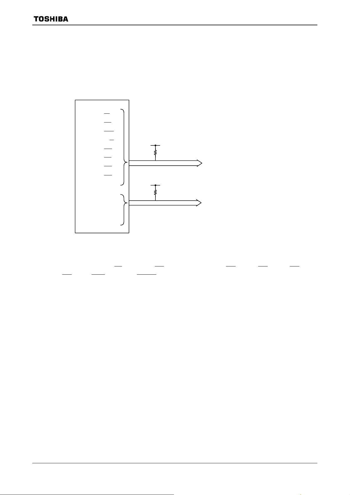
A
TMP91FY42
Figure 3.5.1 shows an example external interface circuit when the bus release function is
used.
When the bus is released, neither the internal memory nor the internal I/O can be accessed.
However, the internal I/O continues to operate. As a result, the watchdog timer also continues
to run. Therefore, the bus release time must be taken into account and care must be taken when
setting the detection time for the WDT.
P30 (RD)
WR
HWR
W/R
CS0 )
CS1 )
CS2 )
CS3
)
)
)
System control bus
)
P31 (
P32 (
P36 (
P40 (
P41 (
P42 (
P43 (
P20 (A16)
∼
P27 (A23)
ddress bus (A23∼A16)
Figure 3.5.1 Interface Circuit Example (Using bus release function)
The above circuit is necessary to set the signal level when the bus is released.
A reset sets P30 (
(
CS3 ) P32 ( HWR ) and P35 (
) and P31 (
RD
BUSAK
) to output, and P40 (
WR
CS0
) to input with pull-up resistor.
), P41 ( CS1 ), P42 ( CS2 ), P43
91FY42-51 2006-11-08
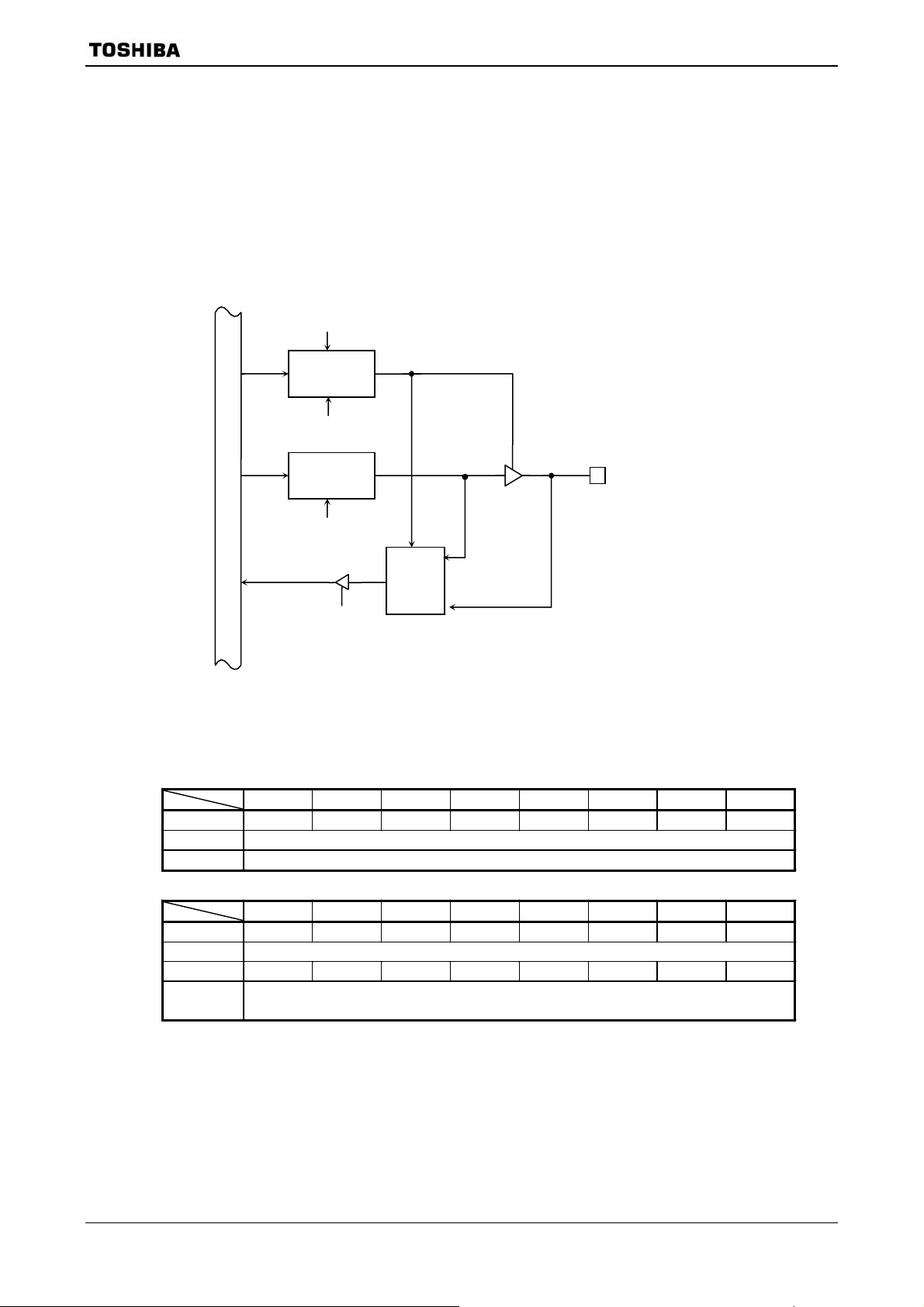
A
3.5.1 Port 0 (P00 to P07)
Port 0 is an 8-bit general-purpose I/O port. Each bit can be set individually for input or
output using the control register P0CR. Resetting resets all bits of the output latch P0, the
control register P0CR to 0 and sets port 0 to input mode. In addition to functioning as a
general-purpose I/O port, port 0 can also function as an Address data bus (AD0 to AD7).
When external memory is accesed, the port automatically functions as the Address data
bus (AD0 to AD7) and all bits of P0CR are cleared to 0.
TMP91FY42
Reset
Direction
control
(on bit basis)
Internal data bus
P0CR write
Output
latch
P0 write
P0 read
S
Selector
B
Output buffer
Port 0
P00∼P07
(AD0∼AD7)
Figure 3.5.2 Port 0
P0
P0
(0000H)
(0000H)
P0CR
(0002H)
Port 0 Register
7 6 5 4 3 2 1 0
Bit symbol P07 P06 P05 P04 P03 P02 P01 P00
Read/Write R/W
After reset Data from external port (Output latch register is cleared to 0.)
Port 0 Control Register
7 6 5 4 3 2 1 0
Bit symbol P07C P06C P05C P04C P03C P02C P01C P00C
Read/Write W
After reset 0 0 0 0 0 0 0 0
Function Port 0 input/output settings
0: Input 1:Output
Note 1: Read-modify-write is prohibited for P0CR.
Note 2: When accessing external, P0CR is AD0 to AD7 and it is cleared to 0.
Figure 3.5.3 Register for Port 0
91FY42-52 2006-11-08

A
3.5.2 Port 1 (P10 to P17)
Port 1 is an 8-bit general-purpose I/O port. Each bit can be set individually for input or
output using the control register P1CR and the function register P1FC. Resetting resets all
bits of the output latch P1, the control register P1CR and the function register P1FC to 0
and sets port 1 to input mode.
In addition to functioning as a general-purpose I/O port, port 1 can also function as an
Address data bus (AD8 to AD15) and Address bus (A8 to A15).
Reset
TMP91FY42
Direction control
(on bit basis)
P1CR write
Internal data bus
Function control
(on bit basis)
P1FC write
Output
latch
P1 write
P1 read
S
Selector
B
Output buffer
Port 1
P10∼P17
(AD8∼AD15/A8∼A15)
Figure 3.5.4 Port 1
91FY42-53 2006-11-08

P0
P1
(0000H)
(0001H)
P1CR
(0004H)
P1FC
(0005H)
Port 1 Register
TMP91FY42
7 6 5 4 3 2 1 0
Bit symbol P17 P16 P15 P14 P13 P12 P11 P10
Read/Write R/W
After reset Data from external port (Output latch register is cleared to 0.)
Port 1 Control Register
7 6 5 4 3 2 1 0
Bit symbol P17C P16C P15C P14C P13C P12C P11C P10C
Read/Write W
After reset 0 0 0 0 0 0 0 0
Function Port 1 function settings
Port 1 Function Register
7 6 5 4 3 2 1 0
Bit symbol P17F P16F P15F P14F P13F P12F P11F P10F
Read/Write W
After reset 0 0 0 0 0 0 0 0
Function Port 1 function settings
Port 1 function settings
Note 1: Read-modify-write is prohibited for P1CR
and P1FC.
Note 2: <P1xF> is bit x in register P1FC; <P1xC>,
in register P1CR.
P1FC<P1xF>
P1CR<P1xC>
0 Input port
1 Output port
Figure 3.5.5 Register for Port 1
0 1
Data bus
(AD15 to AD8)
Address bus
(A15 to A8)
91FY42-54 2006-11-08
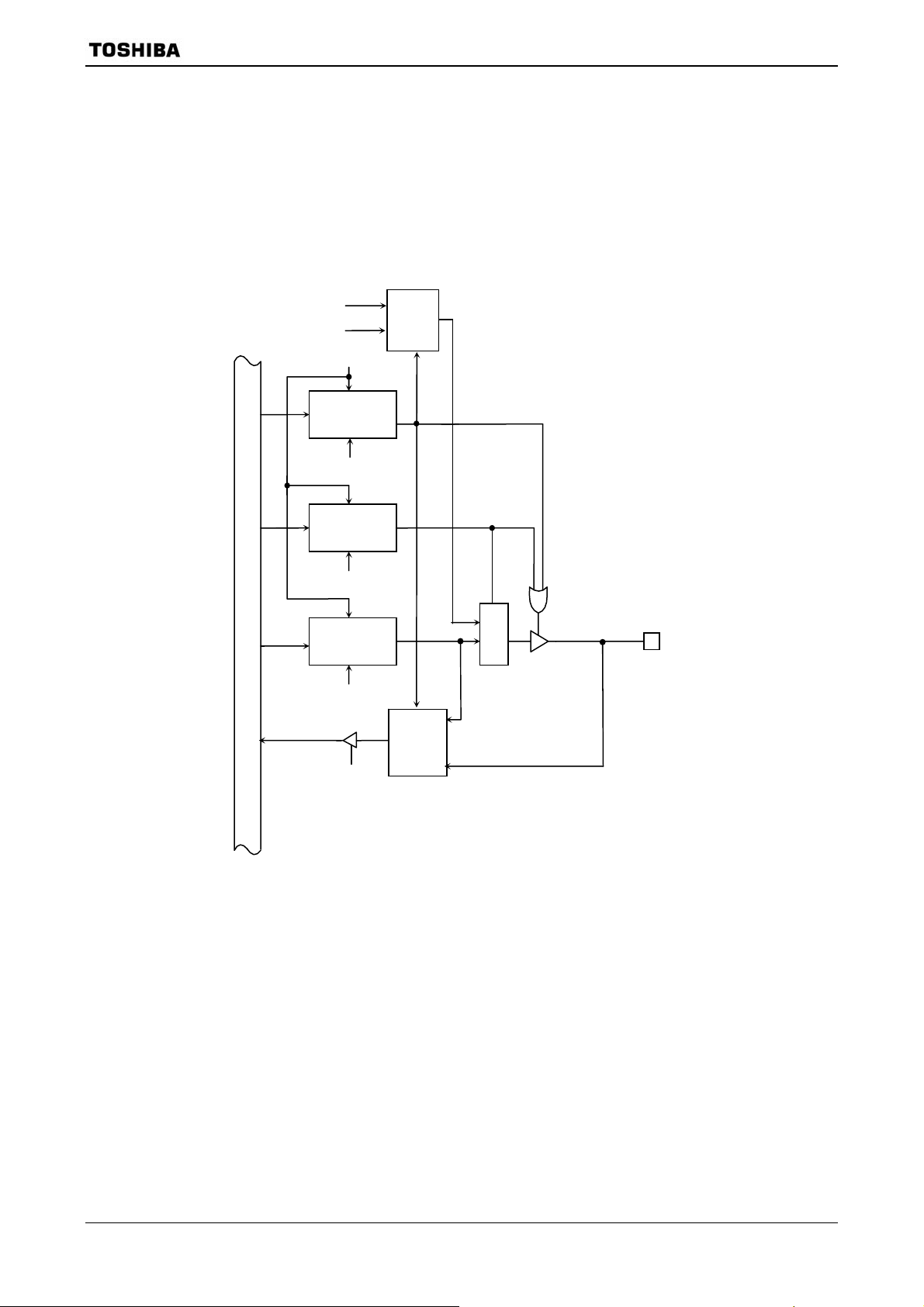
A
A
A
3.5.3 Port 2 (P20 to P27)
Port 2 is an 8-bit general-purpose I/O port. Each bit can be set individually for input or
output using the control register P2CR and the function register P2FC. In addition to
functioning as a general-purpose I/O port, port 2 can also function as an address bus (A0 to
A7) and (A16 to A23).
TMP91FY42
Internal data bus
A16∼A23
A0∼A7
Direction
(on bit basis)
P2CR write
(on bit basis)
P2FC write
P2 write
P2 read
Reset
control
Function
control
Output
latch
B
Selector
S
S
Selector
S
B
Selector
Output buffer
B
Port 2
P20∼P27
(A0∼A7/A16∼A23)
Figure 3.5.6 Port 2
91FY42-55 2006-11-08

P0
P2
(0000H)
(0006H)
P2CR
(0008H)
P2FC
(0009H)
Port 2 Register
TMP91FY42
7 6 5 4 3 2 1 0
Bit symbol P27 P26 P25 P24 P23 P22 P21 P20
Read/Write R/W
After reset Data from external port (Output latch register is set to 1.)
Port 2 Control Register
7 6 5 4 3 2 1 0
Bit symbol P27C P26C P25C P24C P23C P22C P21C P20C
Read/Write W
After reset 0 0 0 0 0 0 0 0
Function Port 2 function settings
Port 2 Function Register
7 6 5 4 3 2 1 0
Bit symbol P27F P26F P25F P24F P23F P22F P21F P20F
Read/Write W
After reset 0 0 0 0 0 0 0 0
Function Port 2 function settings
Port 2 function settings
Note 1: Read-modify-write is prohibited for P2CR
and P2FC.
Note 2: <P2xF> is bit x in register P2FC; <P2xC>,
in register P2CR. To set as an address bus
A23 to A16, set P2FC after setting P2CR.
P2CR<P2xC>
P2FC<P2xF>
0 1
0 Input port
1 Output port
Figure 3.5.7 Register for Port 2
Address bus
(A7 to A0)
Address bus
(A16 to A23)
91FY42-56 2006-11-08

3.5.4 Port 3 (P30 to P37)
Port 3 is an 8-bit general-purpose I/O port. I/O can be set on a bit basis, but note that P30
and P31 are used for output only. I/O is set using control register P3CR and function
register P3FC. Resetting set all bits of output latch P3 to “1”, and control register P3CR
(Bits 0 and 1 are unused), and function register P3FC to “0”. Resetting also outputs 1 frim
P30 and P31, sets P32 to P37 to input mode, and connects a pull-up resistor.
In addition to functioning as a general-purpose I/O port, Port 3 also functions as an I/O
for the CPU’s control/status signal.
When P30 pin is defined as
latch register <P30> to 0 outputs the
P30 pin even when the internal address area is accessed.
If the output latch register <P30> remains 1, the
the external address area is accessed.
TMP91FY42
signal output mode (<P30F> = 1), clearing the output
RD
strobe (used for the pseudo static RAM) from the
RD
strobe signal is output only when
RD
91FY42-57 2006-11-08

A
TMP91FY42
Reset
Function control
(on bit basis)
P3FC write
S
Output
Internal data bus
latch
P3 write
A
B
RD , WR
S
Selector
Output buffer
P30(RD )
P31(
WR )
P3 read
Reset
Direction control
(on bit basis)
P3CR write
Function control
(on bit basis)
P3FC write
Internal data bus
S
Output
latch
P3 write
A
B
HWR , BUSAK , R/ W
S
B
Selector
P3 read
S
Selector
Output buffer
P-ch
Programable
Pull-up
P32(HWR )
P35(
P36(R/
P37
BUSAK )
W )
Figure 3.5.8 Port 3 (P30, P31, P32, P35, P36, P37)
91FY42-58 2006-11-08

A
A
TMP91FY42
Reset
Internal data bus
Direction control
(on bit basis)
P3CR write
S
Output
latch
P3 write
P3 read
S
Selector
Programable
P-ch
Pull-up
P33 ( WAIT )
Output buffer
B
Internal
WAIT
Reset
Direction control
(on bit basis)
P3CR write
Function control
(on bit basis)
P3FC write
Internal data bus
S
Output
latch
P3 write
P3 read
S
Selector
B
P-ch
Programable
Pull-up
P34 (BUSRQ )
Internal
BUSRQ
Figure 3.5.9 Port 3 (P33, P34)
91FY42-59 2006-11-08

P3
(0007H)
P3CR
(000AH)
Port 3 register
TMP91FY42
7 6 5 4 3 2 1 0
Bit symbol P37 P36 P35 P34 P33 P32 P31 P30
Read/Write R/W
After reset Data from external port (Output latch register is set to 1.) 1 1
Function 0 (Output latch register) : Pull-up resistor OFF
1 (Output latch register): Pull-up resistor ON
Port 3 Control register
7 6 5 4 3 2 1 0
Bit symbol P37C P36C P35C P34C P33C P32C
Read/Write W
After reset 0 0 0 0 0 0
Function 0: Input 1: Output
Port 3 Function register
7 6 5 4 3 2 1 0
P3FC
(000BH)
Bit symbol
Read/Write W W
After reset 0 0 0 0 0 0 0
Function Always
−
write “0”
P36F P35F P34F P32F P31F P30F
0: Port
1:
0: Port
1:
BUSAK
WR/
0: Port
1:
BUSRQ
BUSRQ setting
P3FC<P34F> 1
P3CR<P34C> 0
BUSAK setting
P3FC<P35F> 1
P3CR<P35C> 1
WR/ setting
P3FC<P36F> 1
P3CR<P36C> 1
Note 1: Read-modify-write is prohibited for registers P3CR and P3FC.
Note 2: When port P3 is used in the input mode, P3 register controls the built-in
pull-up resistor. Read-modify-write is prohibited in the input mode or the
I/O mode. Setting the built-in pull-up resistor may be depended on the
states of the input pin.
Note 3: When P33/
and Chip Select/ WAIT control register <BnW2:0> to “010”.
pin is used as a
WAIT
pin, set P3CR<P33C> to “0”
WAIT
0: Port
1:
HWR
0: Port
1: WR
P30 (RD) function setting
<P30>
<P30F>
“0” output “1” output
0
Always
RD
1
(for pseudo
SRAM
P31 ( WR ) function setting
<P31>
<P31F>
“0” output “1” output
0
WR
1
access
HWR setting
P3FC<P32F> 1
P3CR<P32C> 1
I/O setting
0 Input
1 Output
0: Port
1: RD
0 1
output
RD
output
0 1
output only for external
only for
external
access
Figure 3.5.10 Register for Port 3
91FY42-60 2006-11-08

A
3.5.5 Port 4 (P40∼P43)
Port 4 is a 4-bit general-purpose I/O port. Each bit can be set individually for input or
output using the control register P4CR and function register P4FC. Resetting, set P40 to
P43 of output register to “1”, the control register P4CR and function register P4FC reset to
“0” and sets port 4 to input mode with pull-up resistor.
In addition to functioning as a general-purpose I/O port, port 4 can also function as chip
select output signal (
Internal data bus
CS0 to CS3 ).
Reset
Direction
control
(on bit
basis)
P4CR write
Function
control
(on bit basis)
P4FC write
S
Output latch
P4 write
P4 read
S
A
B
Selector
CS0 , CS1, CS2 , CS3
S
B
Selector
TMP91FY42
Programmable
pull up
P-ch
P40 ( CS0 ),
Output buffer
P41 (
P42 (
P43 (
CS1),
CS2 ),
CS3 )
Figure 3.5.11 Port4
91FY42-61 2006-11-08

P4
(000CH)
P4CR
(000EH)
P4FC
(000FH)
TMP91FY42
Port 4 Register
7 6 5 4 3 2 1 0
Bit symbol P43 P42 P41 P40
Read/Write R/W
After reset Data from external port
(Output latch register is set to “1”)
Function 0 (Output latch register): Pull-up resistor OFF
1 (Output latch register): Pull-up resistor ON
Port 4 Control Register
7 6 5 4 3 2 1 0
Bit symbol P43C P42C P41C P40C
Read/Write W
0 0 0 0 After reset
0: Input 1: Output
Input/Output setting
0 Input
1 Output
Port 4 Function Register
7 6 5 4 3 2 1 0
Bit symbol P43F P42F P41F P40F
Read/Write W
After reset 0 0 0 0
Function 0: Port 1: CS
0 Port (P40)
1 CS0
0 Port (P41)
1 CS1
Note 1: Read-modify-write instructions are prohibited for registers, P4CR and P4FC.
Note 2: When port 4 is used in Input mode, the P4 register controls the internal pull-up resistor. Read-modify-write
instruction is prohibited in Input mode or I/O mode. Setting the internal pull-up resistor may be depend on the
states of the input pin.
Note 3: When output chip select signal (
register P4FC to “1”.
Note 4: Output latch register is set to “1”, and pull-up resistor is connected.
CS0 to CS3 ), set bit of control register P4 CR to “1” after set bit of function
0 Port (P42)
1 CS2
0 Port (P43)
1 CS3
Figure 3.5.12 Register for Port 4
91FY42-62 2006-11-08
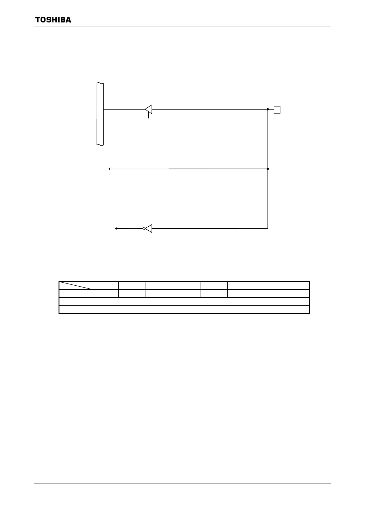
A
A
3.5.6 Port 5 (P50 to P57)
Port 5 is an 8-bit input port and can also be used as the analog input pin for the AD
converter. P53 can also be used as AD trigger input pin for AD converter.
TMP91FY42
P5
(000DH)
Internal data bus
Port 5 read
Port 5
P50∼P57
(AN0∼AN7)
nalog
input
DTRG
(P53 only)
Figure 3.5.13 Port 5
Port 5 Register
7 6 5 4 3 2 1 0
Bit symbol P57 P56 P55 P54 P53 P52 P51 P50
Read/Write R
After reset Data from external port
Figure 3.5.14 Register for Port 5
Note: The input channel selection of AD converter and the permission of AD trigger input of P53 set
by AD converter mode register ADMOD1.
91FY42-63 2006-11-08

A
3.5.7 Port 6 (P60 to P66)
Port 6 are 7-bit general-purpose I/O ports. Resetting set to input port. All bits of output
latch register P6 are set to “1”.
In addition to functioning as an I/O port, port 6 can also function as input or output
function of serial bus interface. This function enable each function by writing “1” to
applicable bit of Port 6 function register P6FC.
Resetting, P6CR and P6FC reset to “0”, all bit set input port.
(1) Port 60 (SCK)
In addition to functioning as an I/O port, port 60 can also function as clock SCK I/O
port in SIO mode of serial bus interface.
Reset
Direction
control
basis)
(on bit
P6CR write
TMP91FY42
Internal data bus
SCK output
Function
control
(on bit basis)
P6FC write
S
Output latch
P6 write
P6 read
A
Selector
B
Selector
Figure 3.5.15 Port 60
S
P60 (SCK)
S
B
SCK input
91FY42-64 2006-11-08

A
TMP91FY42
(2) Port 61 (SO/SDA)
In addition to functioning as an I/O port, port 61 can also function as data SDA I/O
2
port in I
C mode or data SO output pin in SIO mode of serial bus interface.
Reset
Direction
control
(on bit basis)
P6CR write
Function
control
(on bit basis)
P6FC write
S
Internal data bus
SO output
SDA output
Output latch
P6 write
S
A
Selector
B
P61 (SO/SDA)
Open-drain
possible:
ODE<ODE61>
SDA input
Selector
P6 read
Figure 3.5.16 Port 61
S
B
91FY42-65 2006-11-08

A
TMP91FY42
(3) Port 62 (SI/SCL)
In addition to functioning as an I/O port, port 62 can also function as data receiving
2
pin in SIO mode or clock SCL I/O pin in I
C bus mode of serial bus interface.
Reset
Direction
control
(on bit basis)
P6CR write
Function
control
(on bit basis)
P6FC write
S
Internal data bus
Output latch
P6 write
SCL output
S
A
Selector
B
P62 (SI/SCL)
Open-drain
possible:
ODE<ODE62>
S
B
Selector
P6 read
SI input
SCL input
Figure 3.5.17 Port 62
91FY42-66 2006-11-08

A
TMP91FY42
(4) Port 63 (INT0)
In addition to functioning as an I/O port, port 63 can also function as INT0 input pin
of external interrupt.
Reset
Direction
control
(on bit basis)
P6CR write
Function
control
(on bit basis)
P6FC write
Internal data bus
INT0
S
Output latch
P6 write
P6 read
S
B
Selector
Select level/edge
&
Select rising/falling
IIMC<I0LE, I0EDGE>
P63 (INT0)
Figure 3.5.18 Port 63
91FY42-67 2006-11-08

A
A
A
TMP91FY42
(5) Port 64 (SCOUT)
In addition to functioning as an I/O port, port 64 can also function as SCOUT output
pin for outputs internal clock.
Reset
Directin control
(on bit basis)
P6CR write
Functin control
(on bit basis)
P6FC
S
Selector
B
P64 (SCOUT)
Internal data bus
fs clock
f
clock
FPH
Output latch
P6 write
Selector
P6 read
Selector
B
S
SYSCR2<SCOSEL>
S
S
B
A
Figure 3.5.19 Port 64
(6) Port 65, 66
Port 65 and 66 functions as input or output ports.
Reset
Direction
control
(on bit basis)
P6CR write
S
Output latch
S
Internal data bus
P6 write
P6 read
B
Selector
P65
P66
Figure 3.5.20 ポート 65, 66
91FY42-68 2006-11-08

P6
(0012H)
P6CR
(0014H)
P6FC
(0015H)
TMP91FY42
Port 6 Registers
7 6 5 4 3 2 1 0
Bit symbol P66 P65 P64 P63 P62 P61 P60
Read/Write R/W
After reset Data from external port (Output latch register is set to “1”)
Port 6 Control Register
7 6 5 4 3 2 1 0
Bit symbol P66C P65C P64C P63C P62C P61C P60C
Read/Write W
After reset 0 0 0 0 0 0 0
Function 0: Input 1: Output
Port6 I/O setting
0 Input
1 Output
Port 6 Function Register
7 6 5 4 3 2 1 0
Bit symbol P64F P63F P62F P61F P60F
Read/Write W
After reset 0 0 0 0 0
Function 0: Port
1: SCOUT
output
Note: Read-modify-write instructions are prohibited for registers P6CR and P6FC.
0: Port
1: INT0
input
0: Port
1: SCL
output
0: Port
SDA/SO
1:
output
0: Port
1: SCK
output
P60 SCK output setting
P6FC<P60F> 1
P6CR<P60C> 1
P61 SDA/SO output setting
P6FC<P61F> 1
P6CR<P61C> 1
P62 SCL output setting
P6FC<P62F> 1
P6CR<P62C> 1
P63 INT0 input setting
P6FC<P63F> 1
P6CR<P63C> 0
P64 SCOUT output setting
P6FC<P64F> 1
P6CR<P64C> 0
91FY42-69 2006-11-08

ODE
(002FH)
TMP91FY42
Open-drain Output Setting Register
7 6 5 4 3 2 1 0
Bit symbol ODE62 ODE61 ODE93 ODE90
Read/Write R/W
After reset 0 0 0 0
Function
0: Tri-state
1:Open
-drain
0: Tri-state
1:Open
-drain
0: Tri-state
1:Open
-drain
0: Tri-state
1:Open
-drain
Port61 Open-drain output
0 Tri-state output
1 Open-drain output
Port62 Open-drain output
0 Tri-state output
1 Open-drain output
Figure 3.5.21 Register for Port 6
91FY42-70 2006-11-08
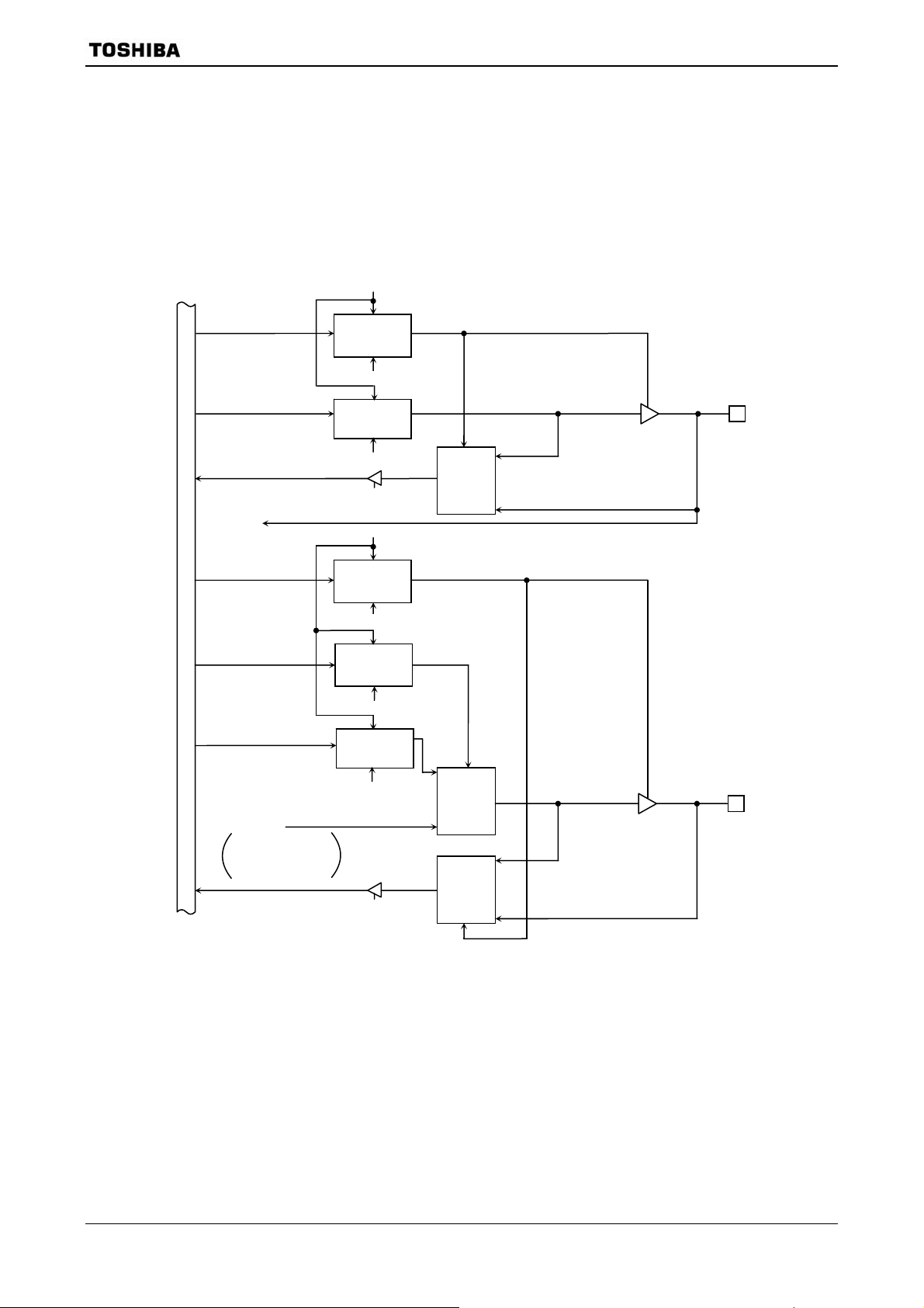
A
A
(
)
(
)
(
)
3.5.8 Port 7 (P70 to P75)
Port 7 is a 6-bit general-purpose I/O port. Resetting set to input port.
In addition to functioning as a I/O port, port 70 and 73 can also function as clock input
pin TA0IN, TA4IN of 8-bit timer 0, 4 and port 71, 72, 74 and 75 can also function 8-bit timer
output pin TA1OUT, TA3OUT, TA5OUT and TA7OUT. This timer output function enable
each function by writing “1” to applicable bit of Port 7 function register P7FC.
Resetting, P7CR and P7FC reset to “0”, all bit set input port.
TA0IN
TA4IN
Internal data bus
Timer F/F OUT
TA1OUT: TMRA01
TA3OUT: TMRA23
TA5OUT: TMRA45
TA7OUT: TMRA67
Reset
Direction
control
on bit basis
P7CR write
S
Output latch
P7 write
P7 read
Reset
Direction
control
on bit basis
P7CR write
Function
control
on bit basis
P7FC write
S
Output latch
P7 write
P7 read
S
Selector
ABS
Selector
Selector
S
TMP91FY42
P70 (TA0IN)
P73 (TA4IN)
B
P71 (TA1OUT)
P72 (TA3OUT)
P74 (TA5OUT)
P75 (TA7OUT)
B
Figure 3.5.22 Port 7
91FY42-71 2006-11-08

P7
(0013H)
P7CR
(0016H)
P7FC
(0017H)
TMP91FY42
Port 7 Register
7 6 5 4 3 2 1 0
Bit symbol P75 P74 P73 P72 P71 P70
Read/Write R/W
After reset Data from external port (Output latch register is set to “1”.)
Port 7 Control Register
7 6 5 4 3 2 1 0
Bit symbol P75C P74C P73C P72C P71C P70C
Read/Write W
After reset 0 0 0 0 0 0
Function 0: Input 1: Output
Port 7 I/O setting
0 Input
1 Output
Port 7 Function Register
7 6 5 4 3 2 1 0
Bit symbol P75F P74F P72F P71F
Read/Write W W
After reset 0 0 0 0
Function 0: Port
TA7OUT
1:
Note 1: Read-Modify-Write instructions are prohibited for the registers P7CR and P7FC.
Note 2: P70/TA0IN and P73/TA4IN pin does not have a register changing Port/Function.
For example, when it is used as an input port, the input signal is inputted to 8-bit timer.
0: Port
TA5OUT
1:
0: Port
TA3OUT
1:
0: Port
TA1OUT
1:
P71 timer out 1 output setting
P7FC<P71F> 1
P7CR<P71C> 1
P72 timer out 3 output setting
P7FC<P72F> 1
P7CR<P72C> 1
P74 timer out 5 output setting
P7FC<P74F> 1
P7CR<P74C> 1
P75 timer out 7 output setting
P7FC<P75F> 1
P7CR<P75C> 1
Figure 3.5.23 Register for Port 7
91FY42-72 2006-11-08

A
A
(
)
(
)
(
)
(
)
3.5.9 Port 8 (P80 to P87)
Port 8 is an 8-bit general-purpose I/O port. Resetting set to input port. All bits of output
latch register P8 are set to “1”.
In addition to functioning as an I/O port, port 8 can also function as clock input of 16-bit
timer, output of 16-bit timer F/F and input function of INT5 to INT8. This function enable
each function by writing “1” to applicable bit of port 8 function register P8FC.
Resetting, P8CR and P8FC reset to “0”, all bits set input port.
(1) P80 to P87
TB0IN0, INT5
TB0IN1, INT6
TB1IN0, INT7
TB1IN1, INT8
Internal data bus
Timer F/F OUT
TB0OUT0: TMRB0
TB0OUT1:TMRB0
TB1OUT0: TMRB1
TB1OUT1: TMRB1
Reset
Direction
control
on bit basis
P8CR write
Function
control
on bit basis
P8FC write
S
Output latch
P8 write
P8 read
Reset
Direction
control
on bit basis
P8CR write
Function
control
on bit basis
P8FC write
S
Output latch
P8 write
P8 read
Selector
ABS
Selector
Selector
S
TMP91FY42
P80
(TB0IN0/INT5)
BS
B
P81
(TB0IN1/INT6)
P84
(TB1IN0/INT7)
P85
(TB1N1/INT8)
P82
(TB0OUT0)
P83
(TB0OUT1)
P86
(TB1OUT0)
P87
(TB1OUT1)
Figure 3.5.24 Port 8 (P80 to P87)
91FY42-73 2006-11-08

P8
(0018H)
P8CR
(001AH)
P8FC
(001BH)
TMP91FY42
Port 8 Register
7 6 5 4 3 2 1 0
Bit symbol P87 P86 P85 P84 P83 P82 P81 P80
Read/Write R/W
After reset Data from external port (Output latch register is set to “1”.)
Port 8 Control Register
7 6 5 4 3 2 1 0
Bit symbol P87C P86C P85C P84C P83C P82C P81C P80C
Read/Write W
After reset 0 0 0 0 0 0 0 0
Function 0: Input 1: Output
Port 8 I/O setting
0 Input
1 Output
Port 8 Function Register
7 6 5 4 3 2 1 0
Bit symbol P87F P86F P85F P84F P83F P82F P81F P80F
Read/Write W
After reset 0 0 0 0 0 0 0 0
Function 0: Port
1: TB1OUT1
Note: Read-modify-write instructions are prohibited for registers P8CR and P8FC.
0: Port
1: TB1OUT0
0: Port
1: TB1IN1
INT8 input
0: Port
1: TB1IN0
INT7 input
0: Port
1: TB0OUT1
0: Port
1: TB0OUT0
0: Port
1: TB0IN1
INT6 input
P82 TB0OUT0 output setting
P8FC<P82F> 1
P8CR<P82C> 1
P83 TB0OUT1 output setting
P8FC<P83F> 1
P8CR<P83C> 1
P86 TB1OUT0 output setting
P8FC<P86F> 1
P8CR<P86C> 1
P87 TB1OUT1 output setting
P8FC<P87F> 1
P8CR<P87C> 1
0: Port
1: TB0IN0
INT5 input
Figure 3.5.25 Register for Port 8
91FY42-74 2006-11-08

3.5.10 Port 9 (P90 to P97)
Ports 90 to 95
Ports 90 to 95 are a 6-bit general-purpose I/O port. Resetting set to input port. All
bits of output latch register are set to “1”.
In addition to functioning as a I/O port, port 90 to 95 can also function as I/O of SIO0,
SIO1. This function enable each function by writing “1” to applicable bit of port 9
function register P9FC.
Resetting, P9CR and P9FC reset to “0”, all bits set input port.
Ports 96 to 97
Ports 96 to 97 are a 2-bit general-purpose I/O port. Case of output port, this is open
drain output. Resetting, output latch register and control register set to “1”, and set to
“High-Z” (High impedance).
In addition to functioning as a I/O port, ports 96 to 97 can also function as
low-frequency oscilator connection pin (XT1 and XT2) during using low speed clock
function. Therefore, dual clock function can use by setting of system clock control
registers SYSCR0 and SYSCR1.
(1) Ports 90 and 93 (TXD0 and TXD1)
In addition to functioning as an I/O port, Ports 90 and 93 can also function as TXD
output pin of serial channel.
TMP91FY42
And P90 and P93 have a programmable open-drain function which can be controlled
by the ODE<ODE90, 93> register.
Reset
Direction
control
(on bit basis)
P9CR write
Function
control
(on bit basis)
P9FC write
Internal data bus
S
Output latch
P9 write
TXD0,
P9 read
ABS
Selector
Selector
P90 (TXD0)
Open-drain
Possible
BS
A
ODE<ODE90, 93>
P93 (TXD1)
Figure 3.5.26 Ports 90 and 93
91FY42-75 2006-11-08

A
A
(2) Ports 91 and 94 (RXD0 and RXD1)
In addition to functioning as an I/O port, ports 91 and 94 can also function as RXD
input pin of serial channel.
Reset
Direction
control
(on bit basis)
P9CR write
TMP91FY42
S
Output latch
Internal data bus
P9 write
P9 read
RXD0,
BS
Selector
P91 (RXD0)
P94 (RXD1)
Figure 3.5.27 Ports 91 and 94
(3) Ports 92 and 95 (
In addition to functioning as an I/O port, ports 92 and 95 can also function as
CTS0 /SCLK0, CTS1 /SCLK1)
CTS
input pin or SCLK I/O pin of serial channel.
Reset
Direction
control
P9CR write
Function
control
(on bit basis)
P9FC write
Internal data bus
SCLK0, 1
output
CTS0 , CTS1
SCLK0, SCLK1 input
Output latch
P9 write
S
P9 read
ABS
Selector
Selector
P92 (SCLK0/ CTS0 )
P95 (SCLK1/
BS
CTS1)
Figure 3.5.28 Port 92, 95
91FY42-76 2006-11-08

)
TMP91FY42
(4) Ports 96 (XT1) and 97 (XT2)
In addition to functioning as an I/O port, ports 96 and 97 can also function as low
frequency oscillator connection pins.
Reset
S
Direction
control
P9CR write
S
Output latch
Output buffer
P9 write
S
B
Selector
P9 read
Internal data bus
Direction
control
(on bit basis)
A
S
(Open-drain
output)
Low-frequency oscillation enable
P96 (XT1)
(ON at 1)
P9CR write
S
Output latch
Output buffer
P9 write
P9 read
Selector
S
B
A
(Open-drain
output)
Figure 3.5.29 Ports 96 and 97
P97 (XT2
Low-frequency clock
91FY42-77 2006-11-08
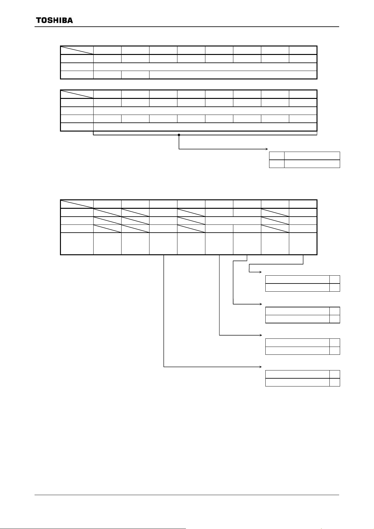
P9
(0019H)
P9CR
(001CH)
P9FC
(001DH)
TMP91FY42
Port 9 Registers
7 6 5 4 3 2 1 0
Bit symbol P97 P96 P95 P94 P93 P92 P91 P90
Read/Write R/W
After reset 1 1 Data from external port (Output latch register is set to “1”.)
Port 9 Control Register
7 6 5 4 3 2 1 0
Bit symbol P97C P96C P95C P94C P93C P92C P91C P90C
Read/Write W
After reset 1 1 0 0 0 0 0 0
Function 0: Input 1: Output
Port9 I/O setting
0 Input
1 Output
Note: Ports 96 and 97 are open-drain output pins.
Port 9 Function Register
7 6 5 4 3 2 1 0
Bit symbol P95F P93F P92F P90F
Read/Write W W W
After reset 0 0 0 0
Function 0: Port
1: SCLK1
output
Note 1: Read-modify-write instructions are prohibited for the registers P9CR and P9FC.
Note 2: When set TXD pin to open-drain output, write “1” to bit0 of ODE register (for TXD 0 pin), or bit1 (for TXD1 pin) .
P91/RXD0 and P94/RXD1 pin does not have a register changing Port/Function.
For example, when it is also used as an input port, the input signal is inputted to SIO as serial receiving data.
Note 3: Low frequency oscillation circuit
To connect a low frequency resonator to ports 96 and 97, it is necessary to set a following procedure to reduce
the consumption power supply.
(Case of resonator connection)
P9CR<P96C, P97C> = “11”, P9<P96:97> = “00”
(Case of oscillator connection)
P9CR<P96C, P97C> = “11”, P9<P96:97> = “10”
0: Port
1: TXD1
0: Port
1: SCLK0
output
0: Port
1: TXD0
P90 TXD0 output setting
P9FC<P90F> 1
P9CR<P90C> 1
P92 SCLK0 output setting
P9FC<P92F> 1
P9CR<P92C> 1
P93 TXD1 output setting
P9FC<P93F> 1
P9CR<P93C> 1
P95 SCLK1 output setting
P9FC<P95F> 1
P9CR<P95C> 1
91FY42-78 2006-11-08

ODE
(002FH)
TMP91FY42
Open-drain Output Setting Register
7 6 5 4 3 2 1 0
Bit symbol ODE62 ODE61 ODE93 ODE90
Read/Write R/W
After reset 0 0 0 0
Function
0: Tri-state
1:Open
-drain
0: Tri-state
1:Open
-drain
0: Tri-state
1:Open
-drain
0: Tri-state
1:Open
-drain
Port90 Open-drain output
0 Tri-state output
1 Open-drain output
Port93 Open-drain output
0 Tri-state output
1 Open-drain output
Figure 3.5.30 Register for Port 9
91FY42-79 2006-11-08
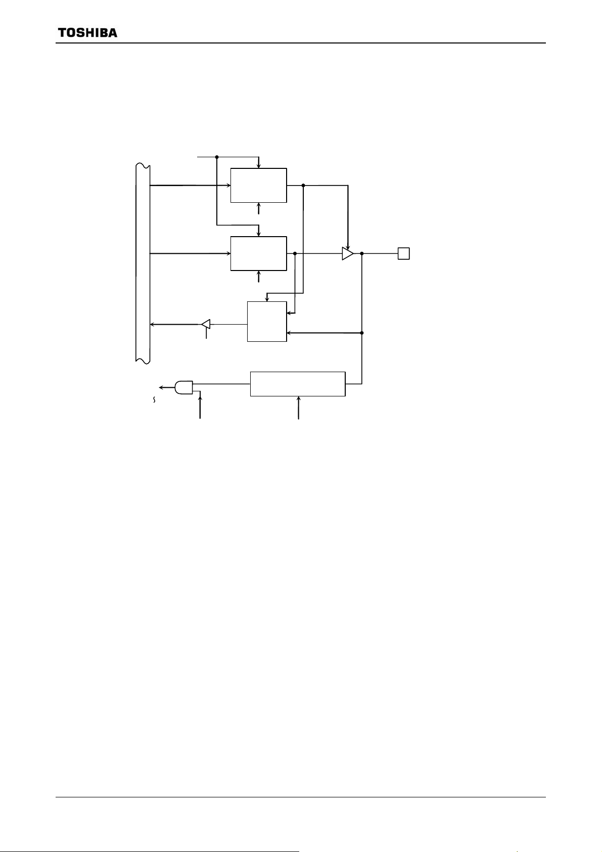
3.5.11 Port A (PA0∼PA7)
Port A is an 8-bit general-purpose I/O port. I/Os can be set on a bit basis by control
register PACR. After reset, PACR is reset to 0 and port A is set to an input port. Port A0 o
A3 can also function as inputs for INT1 to INT4.
Internal data bus
Reset
PA read
Direction
control
(on bit basis)
PACR write
S
Output latch
PA write
S
Selector
TMP91FY42
PA0∼PA3
(INT1∼INT4)
B
A
INT1
~
INT4
PAFC<PA0F,PA1F,PA2F,PA3F> IIMC< I1EDGE, I2EDGE, I3EDGE, I4EDGE>
Rising/Falling edge
detection
Figure 3.5.31 Port A0∼A3
91FY42-80 2006-11-08
Reset
R
irection contro
(on bit basis)
PACR write
S
Output latch
TMP91FY42
PA4∼PA7
Internal data bus
PA read
PA write
S
Selector
B
A
Figure 3.5.32 Port A4∼A7
91FY42-81 2006-11-08
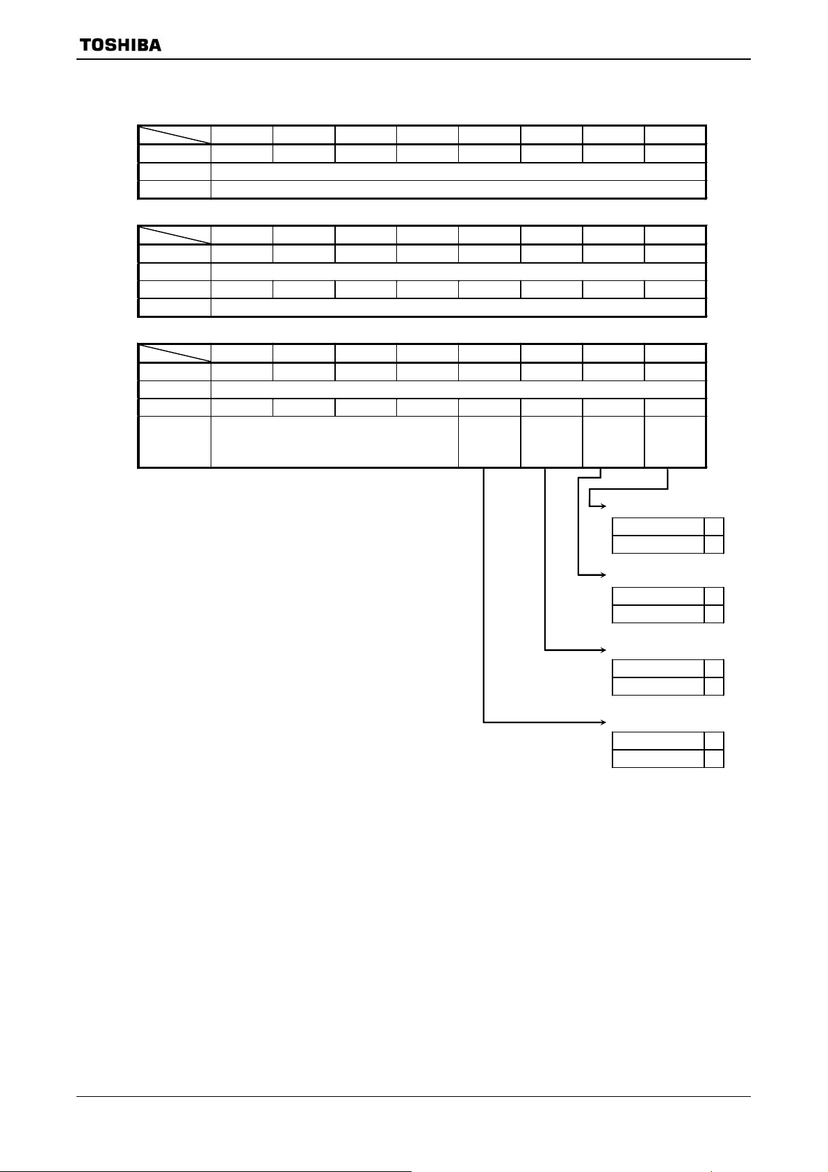
PA
(001EH)
PACR
(0020H)
PAFC
(0021H)
Port A register
TMP91FY42
7 6 5 4 3 2 1 0
Bit symbol PA7 PA6 PA5 PA4 PA3 PA2 PA1 PA0
Read/Write R/W
After reset Dat a from external port (Output latch register is set to “1”)
Port A control register
7 6 5 4 3 2 1 0
Bit symbol PA7C PA6C PA5C PA4C PA3C PA2C PA1C PA0C
Read/Write W
After reset 0 0 0 0 0 0 0 0
Function 0: Input 1: Output
Port A function register
7 6 5 4 3 2 1 0
Bit symbol
Read/Write W
After reset 0 0 0 0 0 0 0 0
Function
− − − −
Always write “0”
PA3F PA2F PA2F PA0F
0: Port
1: INT4
input
0: Port
1: INT3
input
0: Port
1: INT2
input
0: Port
1: INT1
input
PA0 INT1 input setting
PAFC<PA0F> 1
PACR<PA0C> 0
PA1 INT2 input setting
PAFC<PA1F>> 1
PACR<PA1C> 0
PA2 INT3 input setting
PAFC<PA2F> 1
PACR<PA2C> 0
PA3 INT4 input setting
PAFC<PA3F> 1
PACR<PA3C> 0
Note: Read-modify-write is prohibited for registers PACR and PAFC.
Figure 3.5.33 Register for Port A
91FY42-82 2006-11-08

3.6 Chip Select/Wait Controller
On the TM91FY42, four user-specifiable address areas (CS0 to CS3) can be set. The data
bus width and the number of waits can be set independently for each address area (CS0 to
CS3 and others).
The pins
output pins for the areas CS0 to CS3. When the CPU specifies an address in one of these areas,
the corresponding
(in ROM or SRAM). However, in order for the chip select signal to be output, the port 4
function register P4FC must be set. TMP91FY42 supports connection of external ROM and
SRAM.
The areas CS0 to CS3 are defined by the values in the memory start address registers
MSAR0 to MSAR3 and the memory address mask registers MAMR0 to MAMR3.
The chip select/wait control registers B0CS to B3CS and BEXCS should be used to specify
the master enable/disable status the data bus width and the number of waits for each address
area.
The input pin controlling these states is the bus wait request pin (
CS0
to
(which can also function as port pins P40 to P43) are the respective
CS3
CS0 to CS3 pin outputs the chip select signal for the specified address area
TMP91FY42
WAIT ).
3.6.1 Specifying an Address Area
The CS0 to CS3 address areas are specified using the start address registers (MSAR0 to
MSAR3) and memory address mask registers (MAMR0 to MAMR3).
At each bus cycle, a compare operation is performed to determine if the address on the
specified a location in the CS0 to CS3 area. If the result of the comparison is a match, this
indicates an access to the corresponding CS area. In this case, the
outputs the chip select signal and the bus cycle operates in accordance with the settings in
chip select/wait control register B0CS to B3CS. (See 3.6.2 “Chip Select/Wait Control
Registers”.)
CS0 to CS3 pin
91FY42-83 2006-11-08

MSAR0
(00C8H)
MSAR2
(00CCH)
Address
000000H
FFFFFFH
(1) Memory start address registers
Figure 3.6.1 shows the memory start address registers. The memory start address
registers MSAR0 to MSAR3 set the start addresses for the CS0 to CS3 areas. Set the
upper 8 bits (A23 to A16) of the start address in <S23:16>. The lower 16 bits of the
start address (A15 to A0) are permanently set to 0. Accordingly, the start address can
only be set in 64-Kbyte increments, starting from 000000H.
relationship between the start address and the start address register value.
Memory Start Address Registers (for areas CS0 to CS3)
7 6 5 4 3 2 1 0
MSAR1
(00CAH)
MSAR3
(00CEH)
Bit symbol S23 S22 S21 S20 S19 S18 S17 S16
Read/Write R/W
After reset 1 1 1 1 1 1 1 1
Function Determines A23 to A16 of start address.
Figure 3.6.1 Memory Start Address Register
Start address Value in start address register (MSAR0 to MSAR3)
64 Kbytes
000000H ...................... 00H
010000H ...................... 01H
020000H ...................... 02H
030000H ...................... 03H
040000H ...................... 04H
050000H ...................... 05H
060000H ...................... 06H
to to
FF0000H ...................... FFH
TMP91FY42
Figure 3.6.2 shows the
Sets start addresses for areas CS0 to CS3.
Figure 3.6.2 Relationship between Start Address and Start Address Register Value
91FY42-84 2006-11-08
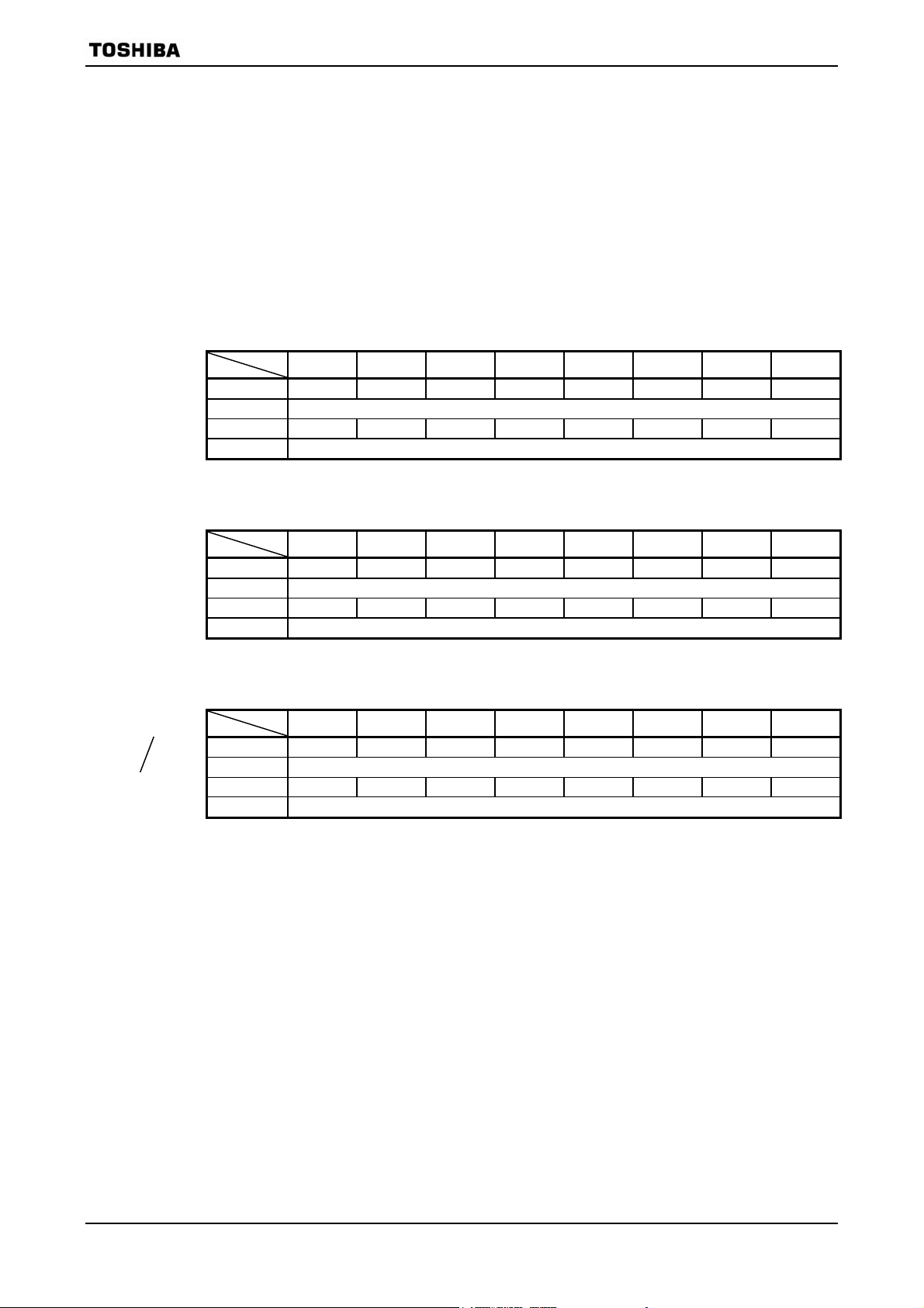
TMP91FY42
(2) Memory address mask registers
Figure 3.6.3 shows the memory address mask registers. Memory address mask
registers MAMR0 to MAMR3 are used to set the size of the CS0 to CS3 areas by
specifying a mask for each bit of the start address set in memory start address
registers MAMR0 to MAMR3. The compare operation used to determine if an address
is in the CS0 to CS3 areas is only performed for bus address bits corresponding to bits
set to 0 in these registers. Also, the address bits that can be masked by MAMR0 to
MAMR3 differ between CS0 to CS3 areas. Accordingly, the size that can be each area
is different.
Memory Address Mask Register (for CS0 area)
7 6 5 4 3 2 1 0
MAMR0
(00C9H)
Bit symbol V20 V19 V18 V17 V16 V15 V14 to V9 V8
Read/Write R/W
After reset 1 1 1 1 1 1 1 1
Function Sets size of CS0 area 0: Used for address compare
Range of possible settings for CS0 area size: 256 bytes to 2 Mbytes
Memory Address Mask Register (CS1)
7 6 5 4 3 2 1 0
MAMR1
(00CBH)
Bit symbol V21 V20 V19 V18 V17 V16 V15 to V9 V8
Read/Write R/W
After reset 1 1 1 1 1 1 1 1
Function Sets size of CS1 area 0: Used for address compare
Range of possible settings for CS1 area size: 256 bytes to 4 Mbytes.
Memory Address Mask Register (CS2, CS3)
7 6 5 4 3 2 1 0
MAMR2
(00CDH)
MAMR3
(00CFH)
Bit symbol V22 V21 V20 V19 V18 V17 V16 V15
Read/Write R/W
After reset 1 1 1 1 1 1 1 1
Function Sets size of CS2 or CS3 area 0: Used for address compare
Range of possible settings for CS2 and CS3 area sizes: 32 Kbytes to 8 Mbytes.
Figure 3.6.3 Memory Addr ess Mask Registers
91FY42-85 2006-11-08
MSAR0
MSMR0
TMP91FY42
(3) Setting memory start addresses and address areas
Figure 3.6.4 show an example of specifying a 64-Kbyte address area starting from
010000H using the CS0 areas.
Set 01H in memory start address register MSAR0<S23:16> (Corresponding to the
upper 8 bits of the start address). Next, calculate the difference between the start
address and the anticipated end address (01FFFFH). Bits 20 to 8 of the result
correspond to the mask value to be set for the CS0 area. Setting this value in memory
address mask register MAMR0<V20:8> sets the area size This example sets 07H in
MAMR0 to specify a 64-Kbyte area.
0 0 0 0 0 0 0 1 1 1 1 1 1 1 1 1 1 1 1 1 1 1 1 1
0 1 F F F F
S23 S22 S21 S20 S19 S18 S17 S16
0 0 0 0 0 0 0 1
0 1 H
0 0 0 0 0 0 0 0 1 1 1 1 1 1 1 1 1 1 1 1 1 1 1 1
0 7 H
V20 V19 V18 V17 V16 V15 V14 to V9 V8
Setting of 07H specifies a 64-Kbyte area.
Memory
end
H
address
Memory
start
address
Memory address
mask register
setting
CS0 area
size
(64 Kbytes)
Figure 3.6.4 Example Showing How to Set the CS0 Area
After a reset, MSAR0 to MSAR3 and MAMR0 to MAMR3 are set to FFH.
B0CS<B0E>, B1CS<B1E> and B3CS<B3E> are reset to 0. This disabling the CS0,
CS1 and CS3 areas. However, as B2CS<B2M> to 0 and B2CS<B2E> to 1, CS2 is
enabled from 000FE0H to 000FFFH to 003000H to FFFFFFH in TMP91FY42. Also,
the bus width and number of waits specified in BEXCS are used for accessing
addresses outside the specified CS0 to CS3 area. (See 3.6.2 “Chip Select/Wait Control
Registers”.)
91FY42-86 2006-11-08

TMP91FY42
(4) Address area size specification
Table 3.6.1 shows the relationship between CS area and area size. “Δ” indicates
areas that cannot be set by memory start address register and address mask register
combinations. When setting an area size using a combination indicated by “Δ”, set the
start address mask register in the desired steps starting from 000000H.
If the CS2 area is set to 16-Mbytes or if two or more areas overlap, the smaller CS
area number has the higher priority.
Example: To set the area size for CS0 to 128 Kbytes:
a. Valid start addresses
000000H
020000H
040000H
060000H
128 Kbytes
128 Kbytes
128 Kbytes
Any of these addresses may be set as the start address.
b. Invalid start addresses
000000H
010000H
030000H
64 Kbytes
128 Kbytes
128 Kbytes
This is not an integer multiple of the desired area size
setting. Hence, none of these addresses can be set as
the start address.
050000H
Table 3.6.1 Valid Area Sizes for Each CS Area
Size (Bytes)
256 512 32 K 64 K 128 K 256 K 512 K 1 M 2 M 4 M 8 M
CS Area
CS0
CS1
CS2
CS3
○ ○ ○ ○
○ ○
○ ○
○ ○
○
Δ Δ Δ Δ Δ
Δ Δ Δ Δ Δ Δ
Δ Δ Δ Δ Δ Δ Δ
Δ Δ Δ Δ Δ Δ Δ
Note: “Δ” indicates areas that cannot be set by memory start address register and address mask
register combinations.
91FY42-87 2006-11-08

3.6.2 Chip Select/Wait Control Registers
Figure 3.6.5 lists the chip select/wait control registers.
The master enable/disable, chip select output waveform, data bus width and number of
wait states for each address area (CS0 to CS3 and others) are set in their respective chip
select/wait control registers, B0CS to B3CS and BEXCS.
TMP91FY42
91FY42-88 2006-11-08

TMP91FY42
B0CS
(00C0H)
Readmodifywrite
instructions
are
prohibited.
B1CS
(00C1H)
Readmodifywrite
instructions
are
prohibited.
B2CS
(00C2H)
Readmodifywrite
instructions
are
prohibited.
B3CS
(00C3H)
Readmodifywrite
instructions
are
prohibited.
BEXCS
(00C7H)
Readmodifywrite
instructions
are
prohibited.
7 6 5 4 3 2 1 0
Bit symbol B0E B0OM1 B0OM0 B0BUS B0W2 B0W1 B0W0
Read/Write W W
After reset 0 0 0 0 0 0 0
Function 0: Disable
1: Enable
Chip select output
waveform selection
00: For ROM/SRAM
01:
10: Don’t care
Data bus
width
0: 16 bits
1: 8 bits
Number of waits
000: 2 waits 100: Reserved
001: 1 wait 101: 3 waits
010: (1 + N) waits 110: 4 waits
011: 0 waits 111: 8 waits
11:
Bit symbol B1E B1OM1 B1OM0 B1BUS B1W2 B1W1 B1W0
Read/Write W W
After reset 0 0 0 0 0 0 0
Function 0: Disable
1: Enable
Chip select output
waveform selection
00: For ROM/SRAM
01:
10: Don’t care
Data bus
width
0: 16 bits
1: 8 bits
Number of waits
000: 2 waits 100: Reserved
001: 1 wait 101: 3 waits
010: (1 + N) waits 110: 4 waits
011: 0 waits 111: 8 waits
11:
Bit symbol B2E B2M B2OM1 B2OM0 B2BUS B2W2 B2W1 B2W0
Read/Write W
After reset 1 0 0 0 0 0 0 0
Functions 0: Disable
1: Enable
CS2 area
selection
0: 16-Mbyte
area
1: CS area
Chip select output
waveform selection
00: For ROM/SRAM
01:
10: Don’t care
Data bus
width
0: 16 bits
1: 8 bits
Number of waits
000: 2 waits 100: Reserved
001: 1 wait 101: 3 waits
010: (1 + N) waits 110: 4 waits
011: 0 waits 111: 8 waits
11:
Bit symbol B3E B3OM1 B3OM0 B3BUS B3W2 B3W1 B3W0
Read/Write W W
After reset 0 0 0 0 0 0 0
Functions 0: Disable
1: Enable
Chip select output
waveform selection
00: For ROM/SRAM
01:
10: Don’t care
Data bus
width
0: 16 bits
1: 8 bits
Number of waits
000: 2 waits 100: Reserved
001: 1 wait 101: 3 waits
010: (1 + N) waits 110: 4 waits
011: 0 waits 111: 8 waits
11:
Bit symbol BEXBUS BEXW2 BEXW1 BEXW0
Read/Write W
After reset 0 0 0 0
Functions Data bus
width
0: 16 bits
1: 8 bits
Number of waits
000: 2 waits 100: Reserved
001: 1 wait 101: 3 waits
010: (1 + N) waits 110: 4 waits
011: 0 waits 111: 8 waits
Master enable bit
0 Enable
1 Disable
CS2 area selection
0 16-Mbyte area
1 Specified address area
Chip select output
waveform selection
00 For ROM/SRAM
01
1011Don’t care
Number of address area waits
(See 3.6.2, (3) Wait control.)
Data bus width selection
0 16-bit data bus
1 8-bit data bus
Figure 3.6.5 Chip Select/Wait Control Registers
91FY42-89 2006-11-08

TMP91FY42
(1) Master enable bits
Bit 7 (<B0E>, <B1E>, <B2E> or <B3E>) of a chip select/wait control register is the
master bit which is used to enable or disable settings for the corresponding address
area. Writing 1 to this bit enables the settings. Reset disables (Sets to 0) <B0E>,
<B1E> and <B3E>, and enabled (Sets to 1) <B2E>. This enables area CS2 only.
(2) Data bus width selection
Bit 3 (<B0BUS>, <B1BUS>, <B2BUS>, <B3BUS> or <BEXBUS>) of a chip
select/wait control register specifies the width of the data bus. This bit should be set
to 0 when memory is to be accessed using a 16-bit data bus and to 1 when an 8-bit
data bus is to be used.
This process of changing the data bus width according to the address being
accessed is known as dynamic bus sizing. For details of this bus operation see
3.6.2.
Table 3.6.2 Dynamic Bus Sizing
Table
Operand Data
Bus Width
8 bits
16 bits
32 bits
Operand Start
Address
(Even number)
2n + 1
(Odd number)
2n + 0
(Even number)
2n + 1
(Odd number)
2n + 0
(Even number)
2n + 1
(Odd number)
Memory Data
Bus Width
8 bits 2n + 0 xxxxx b7 to b0 2n + 0
16 bits 2n + 0 xxxxx b7 to b0
8 bits 2n + 1 xxxxx b7 to b0
16 bits 2n + 1 b7 to b0 xxxxx
16 bits 2n + 0 b15 to b8 b7 to b0
16 bits
8 bits
16 bits
8 bits
16 bits
CPU Address
D15 to D8 D7 to D0
2n + 0 xxxxx b7 to b0 8 bits
2n + 1 xxxxx b15 to b8
2n + 1 xxxxx b7 to b0 8 bits
2n + 2 xxxxx b15 to b8
2n + 1 b7 to b0 xxxxx
2n + 2 xxxxx b15 to b8
2n + 0 xxxxx b7 to b0
2n + 1 xxxxx b15 to b8
2n + 2 xxxxx b23 to b16
2n + 3 xxxxx b31 to b24
2n + 0 b15 to b8 b7 to b0
2n + 2 b31 to b24 b23 to b16
2n + 1 xxxxx b7 to b0
2n + 2 xxxxx b15 to b8
2n + 3 xxxxx b23 to b16
2n + 4 xxxxx b31 to b24
2n + 1 b7 to b0 xxxxx
2n + 2 b23 to b16 b15 to b8
2n + 4 xxxxx b31 to b24
CPU Data
Note: xxxxx indicates that the input data from these bits are ignored during a read. During a write,
indicates that the bus for these bits goes too high impedance; also, that the write strobe signal
for the bus remains inactive.
91FY42-90 2006-11-08

TMP91FY42
(3) Wait control
Bits 0 to 2 (<B0W0:2>, <B1W0:2>, <B2W0:2>, <B3W0:2>, <BEXW0:2>) of a chip
select/wait control register specify the number of waits that are to be inserted when
the corresponding memory area is accessed.
The following types of wait operation can be specified using these bits. Bit settings
other than those listed in the table should not be made.
Table 3.6.3 Wait Operation Settings
<BxW2:0> Number of Waits Wait Operation
000 2
001 1
010 (1 + N)
011 0
100 Reserved Invalid setting
101 3
110 4
111 8
A reset sets these bits to 000 (2 waits).
Inserts a wait of 2 states, irrespective of the
Inserts a wait of 1 state, irrespective of the
Samples the state of the
WAIT pin is low, the waits continue and the bus cycle is extended
the
until the pin goes high.
Ends the bus cycle without a wait, regardless of the
Inserts a wait of 3 states, irrespective of the
Inserts a wait of 4 states, irrespective of the
Inserts a wait of 8 states, irrespective of the
WAIT pin after inserting a wait of 1 state. If
WAIT pin state.
WAIT pin state.
WAIT pin state.
WAIT pin state.
WAIT pin state.
WAIT pin state.
(4) Bus width and wait control for an area other than CS0 to CS3
The chip select/wait control register BEXCS controls the bus width and number of
waits when memory locations which are not in one of the four user-specified address
areas (CS0 to CS3) are accessed. The BEXCS register settings are always enabled for
areas other than CS0 to CS3.
(5) Selecting 16-Mbyte area/specified address area
Setting B2CS<B2M> (Bit 6 of the chip select/wait control register for CS2) to 0
designates the 16-Mbyte area (005000H∼FBFFFFH) as the CS2 area. Setting
B2CS<B2M> to 1 designates the address area specified by the start address register
MSAR2 and the address mask register MAMR2 as CS2 (e.g., if B2CS<B2M> = 1, CS2
is specified in the same manner as CS0, CS1 and CS3 are).
A reset clears this bit to 0, specifying CS2 as a 16-Mbyte address area.
91FY42-91 2006-11-08

TMP91FY42
(6) Procedure for setting chip select/wait control
When using the chip select/wait control function, set the registers in the following
order:
1. Set the memory start address registers MSAR0 to MSAR3.
Set the start addresses for CS0 to CS3.
2. Set the memory address mask registers MAMR0 to MAMR3.
Set the sizes of CS0 to CS3.
3. Set the chip select/wait control registers B0CS to B3CS.
Set the chip select output waveform, data bus width, number of waits and
master enable/disable status for
CS0
to
CS3
.
The CS0 to CS3 pins can also function as pins P40 to P43. To output a chip
select signal using one of these pins, set the corresponding bit in the port 4
function register P6FC to 1.
If a CS0 to CS3 address is specified which is actually an internal I/O and RAM
area address, the CPU accesses the internal address area and no chip select
signal is output on any of the
CS0
to
CS3
pins.
Setting example:
In this example CS0 is set to be the 64-Kbyte area 010000H to 01FFFFH. The bus
width is set to 16 bits and the number of waits is set to 0.
MSAR0 = 01H Start address: 010000H
MAMR0 = 07H Address area: 64 Kbytes
B0CS = 83H ROM/SRAM, 16-bit data bus, 0 waits, CS0 area settings enabled.
91FY42-92 2006-11-08

3.6.3 Connecting External Memory
Figure 3.6.6 shows an example of how to connect external memory to the TMP91FY42.
In this example the ROM is connected using a 16-bit bus. The RAM and I/O are
connected using an 8-bit bus.
74AC573
TMP91FY42
CS0
CS1
CS2
ALE
AD8
AD15
AD0
AD7
~
~
D Q
LE
D Q
LE
CS
OE
Upper byte
ROM
TMP91FY42
Address bus
CS
Lower byte
OE
ROM
CS
OE
8 bit width
RAM
WE
CS
OE
8 bit width
I/O
WE
RD
WR
Figure 3.6.6 Example of External Memory Connection
(ROM uses 16-bit bus; RAM and I/O use 8-bit bus.)
A reset clears all bits of the port 4 control register P4CR and the port 4 function
register P4FC to 0 and disables output of the CS signal. To output the CS signal, the
appropriate bit must be set to 1.
91FY42-93 2006-11-08
3.7 8-Bit Timers (TMRA)
The TMP91FY42 features 8 channel (TMRA0 to TMRA7) built-in 8-bit timers.
These timers are paired into 4 modules: TMRA01, TMRA23, TMRA45 and TMRA67. Each
module consists of 8 channels and can operate in any of the following 4 operating modes.
• 8-bit interval timer mode
• 16-bit interval timer mode
• 8-bit programmable square wave pulse generation output mode (PPG: Variable duty cycle
with variable period)
• 8-bit pulse width modulation output mode (PWM: Variable duty cycle with constant
period)
Figure 3.7.1 to Figure 3.7.3 show block diagrams for TMRA01, TMRA23, TMRA45 and
TMRA67.
Each channel consists of an 8-bit up counter, an 8-bit comparator and an 8-bit timer register.
In addition, a timer flip-flop and a prescaler are provided for each pair of channels.
TMP91FY42
The operation mode and timer flip-flop condition are controlled by 5-byte registers.
We call control registers SFRs: Special function registers.
Each of the four modules (TMRA01, TMRA23, TMRA45 and TMRA67) can be operated
independently. All modules operate in the same manner; hence only the operation of TMRA01
is explained here.
The contents of this chapter are as follows.
3.7.1 Block Diagrams
3.7.2 Operation of Each Circuit
3.7.3 SFRs
3.7.4 Operation in Each Mode
(1) 8-bit timer mode
(2) 16-bit timer mode
(3) 8-bit PPG (Programmable pulse generation) output mode
(4) 8-bit PWM (Pulse width modulation) output mode
(5) Settings for each mode
Table 3.7.1 Registers and Pins for Each Module
Module TMRA01 TMRA23 TMRA45 TMRA67
External
pin
SFR
(Address)
Input pin for
external clock
Output pin for timer
flip-flop
Timer run register TA01RUN (0100H) TA23RUN (0108H) TA45RUN (0110H) TA67RUN (0118H)
Timer register
Timer mode
register
Timer flip-flop
control register
TA0IN
(shared with P70)
TA1OUT
(shared with P71)
TA0REG (0102H)
TA1REG (0103H)
TA01MOD (0104H) TA23MOD (010CH) TA45MOD (0114H) TA67MOD (011CH)
TA1FFCR (0105H)
None
TA3OUT
(shared with P72)
TA2REG (010AH)
TA3REG (010BH)
TA3FFCR
(010DH)
TA4IN
(shared with P73)
TA5OUT
(shared with P74)
TA4REG (0112H)
TA5REG (0113H)
TA5FFCR (0115H)
None
TA7OUT
(shared with P75)
TA6REG (011AH)
TA7REG (011BH)
TA7FFCR
(011DH)
91FY42-94 2006-11-08
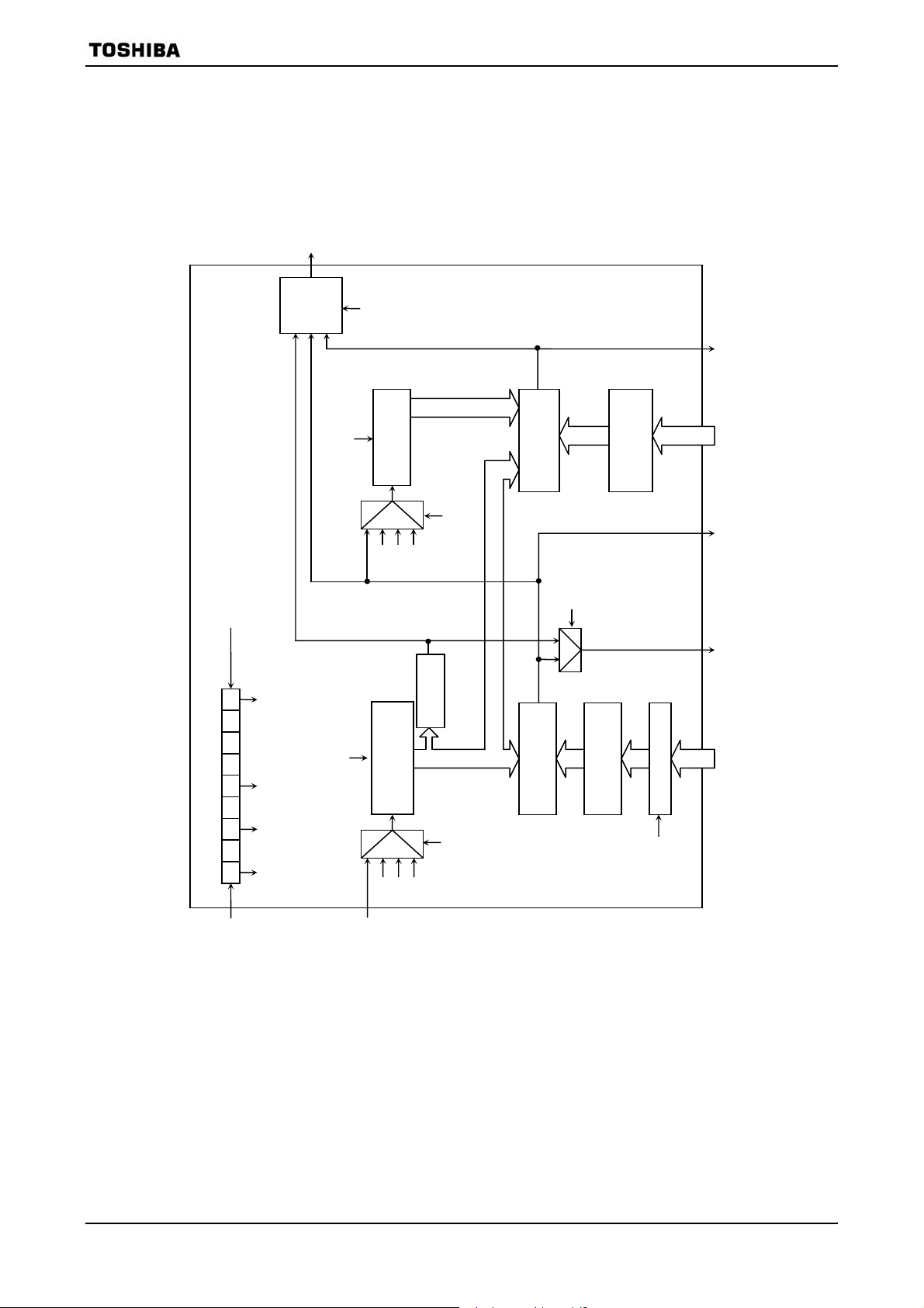
r
3.7.1 Block Diagrams
TA01RUN
<TA01PRUN>
Run/clear Prescaler
512 256 128
64 32 16 8 4 2
Prescale
clock: φT0
φT16 φT256
φT1 φT4
Timer
Timer flip-flop
flip-flop
output: TA1OUT
TA1FF
TA01RUN<TA1RUN>
Selector
TA01RUN<TA0RUN>
Selector
External input
TA1FFCR
φT1
clock: TA0IN
8-bit up counter
φT1
8-bit up counter
(UC1)
φT16
φT256
(UC0)
φT4
φT16
n
Overflow
2
TA01MOD
<TA1CLK1:0>
TA01MOD
<PWM01:00>
TA01MOD
<TA0CLK1:0>
TMP91FY42
TMRA1
interrupt output:
Match
detect
8-bit comparator
TA0TRG
Match
detect
8-bit comparator
(CP1)
TA01MOD
<TA01M1:0>
(CP0)
8-bit timer
TA0REG
8-bit timer register
register
Register buffer 0
TA01RUN
<TA0RDE>
INTTA1
Internal bus
TMRA0
match output:
TA0TRG
TMRA0
interrupt output:
INTTA0
Internal bus
Figure 3.7.1 TMRA01 Block Diagram
91FY42-95 2006-11-08
r
TMP91FY42
Timer flip-flop
output:
TA3OUT
Timer
TA3FF
flip-flop
TA3FFCR
TMRA3
interrup output:
Match
detect
INTTA3
TA23RUN<TA3RUN>>
8-bit up counter
(UC3)
8-bit comparator
(CP3)
TA3REG
8-bit timer register
Internal bus
Selector
φT1
φT16
TA23RUN
<TA23PRUN>
φT256
TA23MOD
<TA3CLK1:0>
TA2TRG
TA23MOD
<TA23M1:0>
TMRA2
match output:
TA2TRG
n
(UC2)
Overflow
2
TA23MOD
<PWM21:20>
TMRA2
interrupt output:
Match
detect
(CP2)
8-bit comparator
TA2REG
8-bit timer register
Register buffer 2
INTTA2
Internal bus
Run/clear Prescale
512 256 128
64 32 16 8 4 2
Prescaler
8-bit up counter
TA23RUN<TA2RUN>
φT1 φT4 φT16 φT256
Selector
φT1
φT4
φT16
TA23MOD
<TA2CLK1:0>
TA23RUN
<TA2RDE>
clock: φT0
Figure 3.7.2 TMRA23 Block Diagram
91FY42-96 2006-11-08
TMP91FY42
Timer flip-flop
output:
TA5OUT
Timer
flip-flop
TA5FF
TA5FFCR
TMRA5
interrup output:
Match
detect
INTTA5
8-bit up counter
φT1
(UC5)
φT16
φT256
n
2
TA45MOD
<TA5CLK1:0>
Overflow
TA45MOD
<PWM21:20>
TA4TRG
Match
(CP5)
8-bit comparator
detect
TA45MOD
<TA45M1:0>
TA5REG
8-bit timer register
Internal bus
TMRA4
match output:
TA4TRG
TMRA4
interrupt output:
INTTA4
TA45RUN<TA5RUN>>
Selector
TA45RUN
<TA45PRUN>
Run/clear Prescaler
512
256 128
64 32 16 8 4 2
Prescaler
T4 φT16 φT256
TA45RUN<TA4RUN>
(UC4)
8-bit up counter
8-bit comparator
(CP4)
TA4REG
8-bit timer register
Register buffer 2
Internal bus
T1
Selector
φT1
φT4
φT16
TA45MOD
<TA4CLK1:0>
TA45RUN
<TA4RDE>
clock: φT0
External input
clock: TA4IN
Figure 3.7.3 TMRA45 Block Diagram
91FY42-97 2006-11-08

r
r
Timer flip-flop
output:
TA7OUT
TMP91FY42
Timer
flip-flop
TA7FF
TA7FFCR
TMRA7
interrup output:
Match
detect
INTTA7
TA67RUN<TA7RUN>>
8-bit up counter
(UC7)
8-bit comparator
(CP7)
TA7REG
8-bit timer register
Internal bus
Selector
φT1
φT16
TA67RUN
<TA67PRUN>
φT256
TA67MOD
<TA7CLK1:0>
TA6TRG
TA67MOD
<TA67M1:0>
TMRA6
match output:
TA6TRG
n
(UC6)
Overflow
2
TA67MOD
<PWM21:20>
TMRA6
interrupt output:
Match
detect
(CP6)
8-bit comparator
TA6REG
8-bit timer register
Register buffer 2
INTTA6
Internal bus
Run/clear Prescale
512 256 128
64 32 16 8 4 2
Prescaler
TA67RUN<TA6RUN>
8-bit up counter
φT1 φT4 φT16 φT256
Selecto
φT1
φT4
φT16
TA67MOD
<TA6CLK1:0>
TA67RUN
<TA6RDE>
clock: φT0
Figure 3.7.4 TMRA67 Block Diagram
91FY42-98 2006-11-08
 Loading...