

TOSHIBA Photocoupler GaAℓAs IRED + Photo IC
A
TLP705
Plasma Display Panel.
Industrial Inverter
IGBT/Power MOS FET Gate Drive
TLP705 consists of a GaAℓAs light emitting diode and a integrated
photodetector.
This unit is 6-lead SDIP package. TLP705 is 50% smaller than 8pin DIP
and has suited the safety standard reinforced insulation class.
So mounting area in safety standard required equipment can be reduced.
TLP705 is suitable for gate driving circuit of IGBT or power MOS FET.
Especially TLP705 is capable of “direct” gate drive of lowr Power IGBTs.
• Peak output current
• Operating frequency
• Guaranteed performance over temperature : −40 to 100°C
• Supply current
• Power supply voltage
• Threshold input current
/ t
• Switching time (t
pLH
) : 200 ns (max)
pHL
• Common mode transient immunity
• Isolation voltage
• UL Recognized
• Construction Mechanical Rating
Creepage Distance
Clearance
Insulation Thickness
7.62-mm pitch
standard type
7.0 mm (min)
7.0 mm (min)
0.4 mm (min)
: ±0.45 A (max)
: 250kHz (max)
: 3mA (max)
: 10 to 20 V
: I
= 8 mA (max)
FLH
:±10 kV/µs(min)
: 5000 Vrms(min)
:UL1577, File No.E67349
10.16-mm pitch
TLPXXXF type
8.0 mm (min)
8.0 mm (min)
0.4 mm (min)
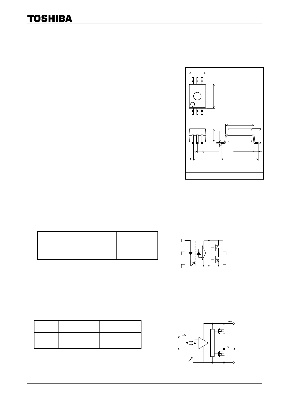
Pin Configuration (Top View)
4.58±0.25
6 5 4
1 2 3
0.4±0.1
TOSHIBA11 -5J1
Weight:0.26 g (typ.)
1
2
TLP705
Unit in mm
6.8±0.25
−0.25
+0.15
3.65
1.27±0.2 1.25±0.25
+0.10
−0.05
0.25±
7.62±0.25
9.7±0.3
6
5
+0.25
11- 5J 1
−0.20
4.0
• Option (D4)
TÜV approved
: EN60747-5-2
Certificate No. R50033433
Maximum operating insulation voltage
: 890 Vpk
Highest permissible over voltage : 8000 Vpk
( Note ) When a EN60747-5-2 approved type is needed,
please designate the “Option(D4)”
Truth Table
Input LED
H ON ON OFF H
L
OFF OFF ON L
Tr1 Tr2 Output
1
3
SHIELD
Schematic
I
F
1+
V
F
3−
SHIELD
0.1 µF bypass capacitor must be connected
between pins 6 and 4. (See Note 6.)
(Tr1)
(Tr2)
ICC
6
V
CC
I
O
5
V
O
4
GND
2006-01-17
TLP705
Maximum Ratings
Forward current IF 20 mA
Forward current derating (Ta ≥ 85°C) ∆IF/∆Ta −0.54 mA/°C
Peak transient forward current (Note 1) IFP 1 A
LED
Reverse voltage VR 5 V
Junction temperature Tj 125 °C
“H” peak output current (Note 2) I
“L” peak output current (Note 2) I
Output voltage VO 25 V
Detector
Supply voltage VCC 25 V
Junction temperature Tj 125 °C
Operating frequency (Note 3) f 250 kHz
Storage temperature range T
Operating temperature range T
Lead soldering temperature (10 s) (Note 4) T
Isolation voltage (AC, 1 minute, R.H. ≤ 60%) (Note 5) BVS 5000 Vrm s
(Ta = 25°C)
Characteristics Symbol Rating Unit
−0.45 A
OPH
0.45 A
OPL
−55 to 125 °C
stg
−40 to 100 °C
opr
260 °C
sol
Note 1: Pulse width PW ≤ 1µs, 300 pps
Note 2: Exponential waveform pulse width PW ≤ 10 µs , f ≤15 kHz
Note 3: Exponential waveform IOPH ≤-0.25 A (≤80 ns) , IOPL ≤+0.25 A (≤80 ns) ,Ta =100 °C
Note 4: It is effective soldering area of Lead .
Note 5: Device considerd a two terminal device: pins 1, 2 and 3 shorted together, and pins 4, 5 and 6 shorted
together.
Note 6: A ceramic capacitor(0.1 µF) should be connected from pin 6 to pin 4 to stabilize the operation of the high
gain linear amplifier. Failure to provide the bypassing may impair the switching property.
The total lead length between capacitor and coupler should not exceed 1 cm.
Recommended Operating Conditions
Characteristics Symbol Min Typ. Max Unit
Input current, ON (Note 7) I
Input voltage, OFF V
Supply voltage VCC 10 ⎯ 20 V
Peak output current I
Operating temperature T
Note 7: Input signal rise time (fall time) < 0.5 µs.
Note 8: If the rising slope of the supply voltage (VCC) for the detector is steep,stable operation
of the internal circuits cannot be guaranteed.
Be sure to set 3.0V/µs or less for a rising slope of the VCC.
10 ⎯ 15 mA
F (ON)
0 ⎯ 0.8 V
F (OFF)
/ I
OPH
OPL
- 40 ⎯ 100 °C
opr
⎯ ⎯ ± 0.15 A
2
2006-01-17
 Loading...