


TCK321G, TCK322G, and TCK323 Load Switch ICs for 2-to-1 Power Multiplexing
1
© 2021
Application Note
TCK321G, TCK322G, and TCK323
Load Switch ICs for 2-to-1 Power Multiplexing
Application Note
Outline:
This application note describes the TCK321G, TCK322G, and TCK323 two-input, one-output load switch
ICs incorporating a multiplexer for selecting between two input power lines.
The power multiplexing function of load switch ICs is ideal for the power management of battery chargers
for mobile devices (e.g., smartphones and tablets) having two charging ports.
Toshiba Electronic Devices & Storage Corporation
2021-02-02

TCK321G, TCK322G, and TCK323 Load Switch ICs for 2-to-1 Power Multiplexing
2
© 2021
Application Note
Table of Contents
Outline: ............................................................................................................................................... 1
Table of Contents ................................................................................................................................ 2
1. Introduction ..................................................................................................................................... 6
2. Application examples for the TCK32*G ........................................................................................... 6
3. Differences among the TCK321G, TCK322G, and TCK323G ......................................................... 7
4. Block diagram of the TCK32*G and descriptions of internal blocks ................................................. 8
4.1. Overvoltage lockout (OVLO) circuit [Figure 4.1(1)] ............................................................................. 8
4.2. Undervoltage lockout (UVLO) circuit [Figure 4.1(2)] ......................................................................... 10
4.3. Inrush current limiting (slew rate control) circuit [Figure 4.1(3)] ........................................................ 11
4.4. Charge pump circuit [Figure 4.1(4)] ................................................................................................... 12
4.5. Reverse current blocking circuit [Figure 4.1(5)] ................................................................................. 12
4.6. Thermal shutdown (TSD) circuit [Figure 4.1(6)] ................................................................................ 13
4.7. FLAG output circuit [Figure 4.1(7)] .................................................................................................... 14
4.8. Other circuit in the TCK32*G ............................................................................................................. 15
4.8.1. Break-before-make circuit ...................................................................................................................15
5. Internal circuits at the control input pins ........................................................................................ 15
5.1. Internal circuit at the CNT pin ............................................................................................................ 15
5.2. Internal circuit at the V
pin ............................................................................................................. 15
SEL
6. Control modes of the TCK32*G ..................................................................................................... 16
6.1. Off Mode ............................................................................................................................................ 16
6.2. Auto Selection mode .......................................................................................................................... 16
6.2.1. Timing diagram of the TCK321G and TCK322G in Auto Selection mode ..........................................17
6.2.2. Timing chart of the TCK323G in Auto Selection mode .......................................................................20
6.3. Manual Selection mode ..................................................................................................................... 22
7. Definitions of the AC characteristics of the TCK32*G .................................................................... 26
7.1. Hold time (t
7.2. V
selection delay time (t
IN
7.3. Break-before-make time (t
7.4. V
7.5. V
OVP off-time (t
OUT
off-time (CNT) (t
OUT
) .................................................................................................................................... 26
HD
) ............................................................................................................ 26
SEL
)........................................................................................................... 26
BBM
) .................................................................................................................... 27
OVP
) .................................................................................................................. 27
OFF
7.6. V
rise time (tr) and V
OUT
fall time (tf) ............................................................................................. 28
OUT
8. Calculating the power dissipation and junction temperature of an IC ............................................. 28
9. Usage considerations .................................................................................................................... 30
9.1. External capacitors ............................................................................................................................ 30
9.2. Board assembly ................................................................................................................................. 30
9.3. Protection circuits ............................................................................................................................... 30
9.4. Power dissipation ............................................................................................................................... 30
10. Conclusion .................................................................................................................................. 31
2021-02-02
Toshiba Electronic Devices & Storage Corporation

TCK321G, TCK322G, and TCK323 Load Switch ICs for 2-to-1 Power Multiplexing
3
© 2021
Application Note
RESTRICTIONS ON PRODUCT USE .............................................................................................. 32
2021-02-02
Toshiba Electronic Devices & Storage Corporation

TCK321G, TCK322G, and TCK323 Load Switch ICs for 2-to-1 Power Multiplexing
4
© 2021
Application Note
List of Figures
Figure 2.1 Example of a multiplexer circuit using the TCK321G, TCK322G and TCK323G ......................... 6
Figure 2.2 Example of a multiplexer circuit composed of discrete devices ................................................... 7
Figure 2.3 Example of a multiplexer circuit composed of non-multiplexing load switch ICs ......................... 7
Figure 4.1 Block diagram of the TCK32*G ..................................................................................................... 8
Figure 4.2 Overvoltage lockout operation ...................................................................................................... 9
Figure 4.3 Example of operations when entering and exiting OVLO mode .................................................. 9
Figure 4.4 Undervoltage lockout operation .................................................................................................. 11
Figure 4.5 Output current waveform when inrush current is limited ............................................................ 12
Figure 4.6 Reverse blocking current (I
)-vs-output voltage (V
RB
) curve of the TCK32*G ........................ 12
OUT
Figure 4.7 Reverse current blocking operation during switching between two power supplies .................. 13
Figure 4.8 Thermal shutdown operation ...................................................................................................... 14
Figure 4.9 Equivalent circuit for the FLAG output ........................................................................................ 14
Figure 4.10 Break-before-make operation ................................................................................................... 15
Figure 5.1 Internal circuit at the CNT pin ..................................................................................................... 15
Figure 5.2 Internal circuit at the V
pin ...................................................................................................... 16
SEL
Figure 6.1 Control modes of the TCK32*G .................................................................................................. 16
Figure 6.2 Timing diagram of the TCK321G and TCK322G in Auto Selection mode ................................. 18
Figure 6.3 Timing diagram of the TCK323G in Auto Selection mode .......................................................... 21
Figure 6.4 Timing diagram of the TCK321G, TCK322G, and TCK323G in Manual Selection mode .......... 24
Figure 7.1 Example of a chattering waveform.............................................................................................. 26
Figure 7.2 Hold time ..................................................................................................................................... 26
Figure 7.3 Definitions of V
Figure 7.4 Definition of V
Figure 7.5 Definition of V
Figure 7.6 Definitions of V
selection time (t
IN
OVP off-time (t
OUT
off-time (t
OUT
rise time (tr) and V
OUT
OFF
) and break-before-make time (t
SEL
) ......................................................................................... 27
OVP
) ................................. 27
BBM
) .................................................................................................. 27
fall time (tf)................................................................. 28
OUT
Figure 8.1 Power dissipation (P
) vs. ambient temperature (Ta) ................................................................. 29
D
2021-02-02
Toshiba Electronic Devices & Storage Corporation

TCK321G, TCK322G, and TCK323 Load Switch ICs for 2-to-1 Power Multiplexing
5
© 2021
Application Note
List of Tables
Table 3.1 Functions available with and differences among the TCK321G, TCK322G, and TCK323G ........ 7
Table 4.1 Comparison of overvoltage lockout thresholds among the TCK32*G ......................................... 10
Table 4.2 Undervoltage lockout thresholds of the TCK32*G ....................................................................... 11
Table 6.1 Operations of the TCK321G, TCK322G, and TCK323G in Off mode ......................................... 16
Table 6.2 Operations of the TCK321G, TCK322G, and TCK323G in Auto Selection mode ....................... 17
Table 6.3 Operations of the TCK321G and TCK322G in Auto Selection mode .......................................... 19
Table 6.4 Operations of the TCK323G in Auto Selection mode .................................................................. 22
Table 6.5 Operations of the TCK321G, TCK322G, and TCK323G in Manual Selection mode .................. 23
Table 6.6 Operations of the TCK321G, TCK322G, and TCK323G in Manual Selection mode .................. 25
2021-02-02
Toshiba Electronic Devices & Storage Corporation
TCK321G, TCK322G, and TCK323 Load Switch ICs for 2-to-1 Power Multiplexing
6
© 2021
Click Here
Click Here
Click Here
Click Here
Click Here
Application Note
1. Introduction
A load switch IC for 2-to-1 power multiplexing (power multiplexer IC) selects between two input
power lines and forwards the selected input to the subsequent IC or circuitry. The TCK321G,
TCK322G, and TCK323G (hereinafter collectively referred to as the TCK32*G) are ideal for the power
management of high-current, high-voltage battery charging applications for smartphones, tablets,
and other mobile devices having two charging ports. The TCK32*G series incorporates inrush current
limiting (slew rate control), thermal shutdown, overvoltage lockout, undervoltage lockout, reverse
current blocking, and flag output functions. Fabricated with a high-voltage CMOS process, the
TCK32*G 2-to-1 power multiplexer ICs support an input voltage up to 36 V. In addition, the TCK32*G
series provides not only Manual Selection mode in which an input power line is selected via an
external control signal but also Auto Selection mode in which an input power line is automatically
selected according to input voltages. The Auto Selection mode eliminates the need for an external
control signal, enabling the TCK32*G series to operate on its own.
This application note describes the functions and operations of the TCK32*G. For details of the
protection functions and other features available with the TCK32*G, see their datasheets.
To download the datasheet for the TCK321G →
To download the datasheet for the TCK322G →
To download the datasheet for the TCK323G →
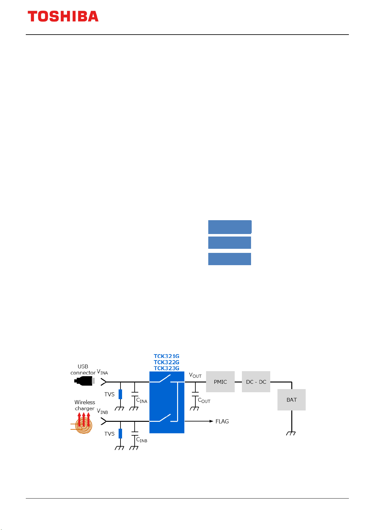
2. Application examples for the TCK32*G
Figure 2.1 shows an example of a multiplexer circuit using the TCK32*G, which selects between
two input power lines and forwards the selected input to the output. This circuit supplies either V
from a USB connector or V
from a wireless charger to a mobile device.
INB
INA
Figure 2.1 Example of a multiplexer circuit using the TCK321G, TCK322G and
TCK323G
2021-02-02
Toshiba Electronic Devices & Storage Corporation

TCK321G, TCK322G, and TCK323 Load Switch ICs for 2-to-1 Power Multiplexing
7
© 2021
Functions available with and differences among the TCK321G, TCK322G, and
(OVLO)
Thermal
Overcurrent
switch-off)
Application Note
Figure 2.2 and Figure 2.3 show equivalent multiplexer circuits using discrete devices and
non-multiplexing load switch ICs, respectively. The use of the TCK32*G, a dedicated power
multiplexer IC, helps reduce parts counts and therefore the system size.
Figure 2.2 Example of a multiplexer circuit
composed of discrete devices
Figure 2.3 Example of a multiplexer
circuit composed of non-multiplexing
load switch ICs
3. Differences among the TCK321G, TCK322G, and TCK323G
The TCK321G, TCK322G, and TCK323G differ in the input power line whose state is indicated by
the FLAG output in Auto Selection mode (V
V
state in the case of the TCK323G) as well as in overvoltage lockout threshold.
INB
Table 3.1
Overvoltage
Part
number
TCK321G 12.0 V
lockout
V
INA
(typ.)
V
12.0 V
(typ.)
Undervoltage
lockout (UVLO)
V
INB
2.6 V
(typ.)
INA
V
2.6 V
(typ.)
INB
state in the case of the TCK321G and TCK322G and
INA
TCK323G
Reverse
Inrush
current
limiting
shutdow
n (TSD)
–
protection
Break-be
fore-ma
ke
current
blocking
(at
FLAG output
(in Auto Selection
mode)
(V
Q
1
INA
) state
TCK322G 15.0 V
(typ.)
TCK323G 15.0 V
(typ.)
15.0 V
(typ.)
15.0 V
(typ.)
2.6 V
(typ.)
2.6 V
(typ.)
2.6 V
(typ.)
2.6 V
(typ.)
–
–
(V
1
2
(V
) state
INA
) state
INB
Q
Q
2021-02-02
Toshiba Electronic Devices & Storage Corporation
TCK321G, TCK322G, and TCK323 Load Switch ICs for 2-to-1 Power Multiplexing
8
© 2021
Application Note
4. Block diagram of the TCK32*G and descriptions of internal blocks
Figure 4.1 Block diagram of the TCK32*G
4.1. Overvoltage lockout (OVLO) circuit [Figure 4.1(1)]
When either V
V
outputs to protect the ICs and circuits connected to them. The OVLO circuit is tripped when V
OUT
or V
exceeds the overvoltage lockout rising threshold (V
INB
below the overvoltage lockout falling threshold (V
The OVLO circuit compares V
(V
) as shown in Figure 4.2. When V
REF
comparator output is toggled, then turning off the V
MOSFET for reference voltage (comparator input) selection turns on, then the reference voltage
switches to V
OVDET_r
toggled again, turning the V
INA
or V
exceeds a threshold, the overvoltage lockout (OVLO) circuit turns off the
INB
. When V
or V
INA
or V
INA
outputs back on.
OUT
with a voltage derived by dividing the reference voltage
INB
or V
INA
drops below V
INB
). Then, when V
OVL_RI
OLV_FA
exceeds the divided reference voltage (V
INB
), the V
outputs. At the same time, the N-channel
OUT
OVDET_r
output turns back on automatically.
OUT
again, the comparator output is
INA
or V
drops
INB
OVDET
), the
INA
2021-02-02
Toshiba Electronic Devices & Storage Corporation

TCK321G, TCK322G, and TCK323 Load Switch ICs for 2-to-1 Power Multiplexing
9
© 2021
IN
OUT
Entering OVLO mode
Exiting OVLO mode
Application Note
Figure 4.2 Overvoltage lockout operation
When recovering from overvoltage lockout, the OVLO circuit allows a hold time of 15 ms typical to
prevent a false output due to input chattering as shown in 4.3.
Test conditions: C
= 1 μF, C
= 1 μF, RL = 50 Ω
15 ms
Figure 4.3 Example of operations when entering and exiting OVLO mode
2021-02-02
Toshiba Electronic Devices & Storage Corporation
TCK321G, TCK322G, and TCK323 Load Switch ICs for 2-to-1 Power Multiplexing
10
© 2021
Ta = 25°C
Ta = 40 to 85°C
Min
Typ.
Max
Min
Max
threshold
threshold
threshold
threshold
threshold
threshold
Application Note
Table 4.1 Comparison of overvoltage lockout thresholds among the TCK32*G
Part
number
TCK321G
TCK322G
TCK323G
Characteristics Symbol Test Condition
Overvoltage lockout
V
(OVLO) rising
Overvoltage lockout
(OVLO) falling
Overvoltage lockout
(OVLO) rising
Overvoltage lockout
(OVLO) falling
Overvoltage lockout
(OVLO) rising
Overvoltage lockout
(OVLO) falling
– – 12.0 – 10.5 13.5 V
OVL_RI
V
V
V
V
V
– –
OVL_FA
– – 15.0 – 13.4 16.6 V
OVL_RI
– –
OVL_FA
– – 15.0 – 13.4 16.6 V
OVL_RI
– –
OVL_FA
V
OVL_RI
- 0.5
V
OVL_RI
- 0.5
V
OVL_RI
- 0.5
4.2. Undervoltage lockout (UVLO) circuit [Figure 4.1(2)]
– – V
–
– – V
–
– – V
–
Unit
When either V
connected to the V
prevent system malfunction. The UVLO circuit is tripped when either V
undervoltage lockout falling threshold voltage (V
or V
compares V
rises back above V
INB
INA
Figure 4.4. When V
output is toggled, then the V
INA
or V
or V
outputs, the undervoltage lockout (UVLO) circuit turns off the V
OUT
with a voltage derived by dividing the reference voltage (V
INB
or V
INA
drops below the minimum operating voltage of the ICs or circuits
INB
or V
INA
UVL_FA
, the V
UVL_RI
drops below the divided reference voltage (V
INB
outputs turn off. At the same time, the N-channel MOSFET for
OUT
outputs turn back on automatically. The UVLO circuit
OUT
). The UVLO circuit has hysteresis. When V
UVDET
reference voltage selection turns off, then the reference voltage switches to V
V
rises back above V
INB
UVDET_r
, the comparator is toggled again, turning the V
outputs to
OUT
drops below the
INB
) as shown in
REF
), the comparator
UVDET_r
OUT
. When V
outputs back on.
INA
INA
or
2021-02-02
Toshiba Electronic Devices & Storage Corporation

TCK321G, TCK322G, and TCK323 Load Switch ICs for 2-to-1 Power Multiplexing
11
© 2021
Ta = 25°C
Ta = -40 to 85°C
Min
Typ.
Max
Min
Max
Undervoltage lockout
threshold
Undervoltage lockout
threshold
Application Note
Figure 4.4 Undervoltage lockout operation
Table 4.2 Undervoltage lockout thresholds of the TCK32*G
Part
number
TCK321G
TCK322G
TCK323G
Characteristics Symbol Test Condition
(UVLO) rising
(UVLO) falling
V
– – 2.9 – 2.3 3.5 V
UVL_RI
V
– –
UVL_FA
V
UVL_RI
- 0.3
– – V
–
Unit
4.3. Inrush current limiting (slew rate control) circuit [Figure 4.1(3)]
Inrush current is limited by a slew rate control circuit. When a large capacitive load is connected to
the output MOSFET, its turning on at high speed causes a large current to flow to charge the load. At
this time, V
load switch IC, it may cause system instability or malfunction. To prevent this situation, the inrush
current limiting circuit turns on the output MOSFET at a low slew rate, and charging slowly the
drops instantaneously because of the impedance of board traces on the VDD side of a
IN
capacitive load. Thereby it ensures a stable system start-up.
2021-02-02
Toshiba Electronic Devices & Storage Corporation

TCK321G, TCK322G, and TCK323 Load Switch ICs for 2-to-1 Power Multiplexing
12
© 2021
Figure 4.5 Output current waveform when inrush current is limited
4.4. Charge pump circuit [Figure 4.1(4)]
Application Note
CL=1μF
CL=100μF
CL=1000μF
The charge pump circuit is a voltage booster that generates a voltage for driving the gate of the
N-channel MOSFET.
4.5. Reverse current blocking circuit [Figure 4.1(5)]
While the internal MOSFET switch is off, the reverse current blocking circuit prevents current
from flowing in the reverse direction from V
circuit is disabled while the MOSFET is on.
OUT
to V
INA
or V
when V
INB
INA
or V
INB
< V
OUT
. This
Figure 4.6 Reverse blocking current (IRB)-vs-output voltage (V
) curve of
OUT
the TCK32*G
2021-02-02
Toshiba Electronic Devices & Storage Corporation

TCK321G, TCK322G, and TCK323 Load Switch ICs for 2-to-1 Power Multiplexing
13
© 2021
Figure 4.7 Reverse current blocking operation during switching between two
power supplies
4.6. Thermal shutdown (TSD) circuit [Figure 4.1(6)]
The thermal shutdown (TSD) circuit monitors the junction temperature to protect the
Application Note
TCK32*G. When the junction temperature exceeds a threshold, the TSD circuit turns off the V
OUT
outputs to prevent the TCK32*G from degrading or being damaged permanently. The TSD circuit
detects the junction temperature by comparing a diode’s forward voltage (V
voltage (V
TCK32*G is operating properly, VF is higher than V
) that is hardly affected by temperature as shown in Figure 4.8(a). When the
TSD
. The diode’s forward voltage has a
TSD
) with a reference
F
temperature coefficient of roughly -2 mV/°C. When the junction temperature reaches 158°C
typical, V
At this point, the TSD circuit switches the reference voltage from V
drops below V
F
. This causes the comparator output to toggle, and the IC turned off.
TSD
TSD
to V
via the
TSD_r
comparator’s output signal. Once the TCK32*G turns off, its power consumption decreases
considerably, it causes the junction temperature to decrease. When a decrease of junction
temperature causes V
to rise above V
F
TSD_r
, the V
outputs turn back on automatically. The
OUT
TSD circuit has a hysteresis of 15°C typical, i.e., there is a temperature difference of 15°C
between the junction temperature at which TSD is tripped to turn off the V
outputs and the
OUT
junction temperature at which TSD is recovered.
2021-02-02
Toshiba Electronic Devices & Storage Corporation

TCK321G, TCK322G, and TCK323 Load Switch ICs for 2-to-1 Power Multiplexing
14
© 2021
Pull up resistor
To PMIC and MCU
Application Note
Figure 4.8 Thermal shutdown operation
4.7. FLAG output circuit [Figure 4.1(7)]
When the overvoltage or undervoltage lockout circuit is tripped, the FLAG output pin transitions
from Low to High to warn a power management IC (PMIC) and other external IC of a system fault.
Since the FLAG output has an open drain configuration, an external pull up resistor should be
connected to the FLAG output. Select a pull up resistor, the resistance value should be determined in
consideration of the sink current of the FLAG output and fully evaluate it with an actual board. (In the
datasheet, V
is specified as 0.4 V maximum when I
OL
SINK
= 1 mA.)
2021-02-02
Toshiba Electronic Devices & Storage Corporation
Figure 4.9 Equivalent circuit for the FLAG output

TCK321G, TCK322G, and TCK323 Load Switch ICs for 2-to-1 Power Multiplexing
15
© 2021
Application Note
4.8. Other circuit in the TCK32*G
4.8.1. Break-before-make circuit
The TCK32*G incorporates two switches. After the TCK32*G “breaks” one switch, the
break-before-make circuit keeps two switches off until it “makes” the other switch. This prevents two
voltage domains from being short-circuited during the changeover between two switches.
Figure 4.10 Break-before-make operation
5. Internal circuits at the control input pins
5.1. Internal circuit at the CNT pin
A pull-down resistor with a typical value of 500 kΩ is internally connected between the CNT and
GND pins.
Figure 5.1 Internal circuit at the CNT pin
5.2. Internal circuit at the V
A resistor with a typical value of 500 kΩ and a MOSFET for voltage conversion are internally
connected to the V
pin. This resistor is pulled up to an internal 3-V power supply(VOP).
SEL
SEL
pin
2021-02-02
Toshiba Electronic Devices & Storage Corporation

TCK321G, TCK322G, and TCK323 Load Switch ICs for 2-to-1 Power Multiplexing
16
© 2021
Independent of the voltages at
V
INA
and V
INB
Reverse current
blocking
V
: Valid
V
INB
: Valid
Application Note
(VOP)
Figure 5.2 Internal circuit at the V
SEL
pin
6. Control modes of the TCK32*G
The TCK32*G can be configured into Off, Auto Selection or Manual Selection mode via the Mode
Control (CNT) and Input Selector (V
characteristics. The following subsections describe the operation in each mode.
Figure 6.1 Control modes of the TCK32*G
6.1. Off Mode
Table 6.1 Operations of the TCK321G, TCK322G, and TCK323G in Off mode
) inputs while taking advantage of the break-before-make
SEL
When V
Input voltage
Output voltage Off (Disabled)
FLAG output Off (High-Z)
= Low and V
CNT
SEL
= Low
INA
6.2. Auto Selection mode
The TCK32*G is configured into Auto Selection mode when V
mode, the TCK32*G transfers the voltage at the V
inputs to the V
INA
are within the normal voltage range. However, the TCK32*G transfers the voltage at the V
to the V
outputs if V
OUT
is in the overvoltage or undervoltage lockout range. The FLAG output
INA
differs among the TCK321G, TCK322G, and TCK323G as shown below.
is Low and V
CNT
outputs if both V
OUT
is High. In this
SEL
INA
and V
inputs
INB
INB
2021-02-02
Toshiba Electronic Devices & Storage Corporation

TCK321G, TCK322G, and TCK323 Load Switch ICs for 2-to-1 Power Multiplexing
17
© 2021
When V
CNT
= Low and V
SEL
is High
range
range
range
range
On
(V
OUT=VINA
)
On
(V
OUT=VINA
)
On
(V
OUT=VINB
)
Off
(Disabled)
FLAG output
TCK321G: Indicates
the V
INA
state
On
(Low)
On
(Low)
Off
(High-Z)
Off
(High-Z)
TCK322G: Indicates
the V
INA
state
On
(Low)
On
(Low)
Off
(High-Z)
Off
(High-Z)
TCK323G: Indicates
the V
INB
state
Off
(High-Z)
Off
(High-Z)
On
(Low)
Off
(High-Z)
V
: Invalid
V
INB
: Valid
V
: Invalid
V
INB
: Valid
V
: Valid
V
INB
: Invalid
V
: Valid
V
INB
: Valid
Outside the operating voltage range: V
UVL_FA>VIN*
or V
IN*>VOVL_RI
Application Note
Table 6.2 Operations of the TCK321G, TCK322G, and TCK323G in Auto Selection
mode
V
Input voltage
Output voltage
: In the
INA
operating voltage
range
: In the
V
INB
operating voltage
V
: In the
INA
operating voltage
range
: Outside the
V
INB
operating voltage
V
: Outside the
INA
operating voltage
range
: In the
V
INB
operating voltage
V
: Outside the
INA
operating voltage
range
: Outside the
V
INB
operating voltage
Reverse current blocking
INA
In the operating voltage range: V
ULV_RI<VIN*<VOVL_RI
INA
INA
INA
6.2.1. Timing diagram of the TCK321G and TCK322G in Auto Selection mode
In the case of the TCK312G and TCK322G, the FLAG output indicates the V
Selection mode regardless of the V
state. The FLAG output remains Low while V
INB
state in Auto
INA
is in the normal
INA
voltage range, and is driven High when the overvoltage or undervoltage lockout circuit is tripped. See
Section 7.1 for a description of its hold time (t
HD
).
2021-02-02
Toshiba Electronic Devices & Storage Corporation

TCK321G, TCK322G, and TCK323 Load Switch ICs for 2-to-1 Power Multiplexing
18
© 2021
Application Note
Figure 6.2 Timing diagram of the TCK321G and TCK322G in Auto Selection mode
2021-02-02
Toshiba Electronic Devices & Storage Corporation

TCK321G, TCK322G, and TCK323 Load Switch ICs for 2-to-1 Power Multiplexing
19
© 2021
** V
OUT
turns on after break-before-make time (t
BBM
).
V
OUT
FLAG
Input voltage
selected
(a) L H L H
Off – Hz
–
(b) L H L L
Off – Hz
–
(c) L H L M
On
(*)
V
INB
Hz
–
(d) L H L H
Off – Hz
–
(e) L H L M
On
(*)
V
INB
Hz
–
(f) L H L L
Off – Hz
–
(g) L H H L
Off – Hz
–
(h) L H L L
Off – Hz
–
(i) L H M L
On
(*)
V
INA
Hz → Low
V
INA
(j) L H H L
Off
–
Low → Hz
V
INA
(k) L H M L
On
(*)
V
INA
Hz → Low
V
INA
(l) L H L L
Off
–
Low → Hz
V
INA
(m) L H L M
Off – Hz
–
(n) L H M M
On
(*)
V
INA
Hz→ Low
V
INA
(o) L H L M
On
(**)
V
INB
Low → Hz
V
INA
(p) L H M M
On
(**)
V
INA
Hz → Low
V
INA
(q) L H H M
On
(**)
V
INB
Low → Hz
V
INA
(r) L H M M
On
(**)
V
INA
Hz → Low
V
INA
(s) L H M H
On
V
INA
Low
V
INA
(t) L H M M
On
V
INA
Low
V
INA
(u) L H M L
On
V
INA
Low
V
INA
(v)
L
H → L L L
Off
–
Low → Hz
V
INA
Application Note
Table 6.3 Operations of the TCK321G and TCK322G in Auto Selection mode
* V
turns on after hold time (tHD).
OUT
Period V
CNT
V
SEL
V
INA
V
INB
V
OUT
output
FLAG output Input state indicated
2021-02-02
M: In the normal voltage range
Hz: High impedance
H: In the overvoltage lockout range
L: In the undervoltage lockout range
Toshiba Electronic Devices & Storage Corporation

TCK321G, TCK322G, and TCK323 Load Switch ICs for 2-to-1 Power Multiplexing
20
© 2021
6.2.2. Timing chart of the TCK323G in Auto Selection mode
Application Note
In the case of the TCK323G, the FLAG output indicates the V
regardless of the V
state. The FLAG output remains Low while V
INA
state in Auto Selection mode
INB
is in the normal voltage range,
INB
and is driven High when the overvoltage or undervoltage lockout circuit is tripped. See Section 7.1 for
a description of its hold time (t
HD
).
2021-02-02
Toshiba Electronic Devices & Storage Corporation

TCK321G, TCK322G, and TCK323 Load Switch ICs for 2-to-1 Power Multiplexing
21
© 2021
Application Note
Figure 6.3 Timing diagram of the TCK323G in Auto Selection mode
2021-02-02
Toshiba Electronic Devices & Storage Corporation

22
© 2021
* V
OUT
turns on after hold time (tHD).
** V
turns on after break-before-make time (t
).
V
OUT
FLAG
Input voltage
selected
(a) L H L H
Off – Hz
–
(b) L H L L
Off – Hz
–
(c) L H L M
On
(*)
V
INB
Hz → Low
V
INB
(d) L H L H
Off – Hz
–
(e) L H L M
On
(*)
V
INB
Hz → Low
V
INB
(f) L H L L
Off – Hz
–
(g) L H H L
Off – Hz
–
(h) L H L L
Off – Hz
–
(i) L H M L
On
(*)
V
INA
Hz
–
(j) L H H L
Off – Hz
–
(k) L H M L
On
(*)
V
INA
Hz
–
(l) L H L L
Off – Hz
–
(m) L H L M
Off – Hz
–
(n) L H M M
On
(*)
V
INA
Hz
–
(o) L H L M
On
(**)
V
INB
Hz → Low
V
INB
(p) L H M M
On
(**)
V
INA
Hz
–
(q) L H H M
On
(**)
V
INB
Hz → Low
(r) L H M M
On
(**)
V
INA
Low → Hz
V
INB
(s) L H M H
On
V
INA
Hz
–
(t) L H M M
On
V
INA
Hz
–
(u) L H M L
On
V
INA
Hz
–
(v)
L
H → L L L
Off – Hz
–
OUT
TCK321G, TCK322G, and TCK323 Load Switch ICs for 2-to-1 Power Multiplexing
Application Note
Table 6.4 Operations of the TCK323G in Auto Selection mode
BBM
Period V
CNT
V
SEL
V
INA
V
INB
V
OUT
output
FLAG output Input state indicated
M: In the normal voltage range
Hz: High impedance
H: In the overvoltage lockout range
L: In the undervoltage lockout range
6.3. Manual Selection mode
The TCK321G, TCK322G, and TCK323G operate identically in Manual Selection mode. In this mode,
either V
V
pin. V
SEL
is High, and both V
(V
CNT
TCK321G, TCK322G, and TCK323G are disabled, turning off the V
undervoltage lockout protection is tripped because of an abnormal V
output is driven Low to indicate it externally. See Section 7.1 for a description of its hold time (t
INA
or V
INA
can be selectively forwarded to the V
INB
is selected when the Mode Control signal (V
INA
and V
are in the normal range. V
INB
) is High and the Input Selector signal (V
outputs via a control signal applied to the
OUT
) is High, the Input Selector signal (V
CNT
is selected when the Mode Control signal
INB
) is Low. When both V
SEL
OUT
CNT
and V
are Low, the
SEL
outputs. When overvoltage or
INA
or V
condition, the FLAG
INB
SEL
HD
)
).
2021-02-02
Toshiba Electronic Devices & Storage Corporation

TCK321G, TCK322G, and TCK323 Load Switch ICs for 2-to-1 Power Multiplexing
23
© 2021
When
CNT
SEL
INA
range
range
range
range
On
(V
OUT=VINA
)
On
(V
OUT=VINA
)
Off
(Disabled)
Off
(Disabled)
FLAG output
Off
(High-Z)
On
(Low)
On
(Low)
On
(Low)
Off
(High-Z)
On
(Low)
On
(Low)
On
(Low)
Off
(High-Z)
On
(Low)
On
(Low)
On
(Low)
V
: Invalid
V
INB
: Valid
V
: Invalid
V
INB
: Valid
V
: Valid
V
INB
: Valid
V
: Valid
V
INB
: Valid
Outside the operating voltage range: V
UVL_FA>VIN*
or V
IN*>VOVL_RI
When
CNT
SEL
INB
is active
range
range
range
range
On
(V
OUT=VINB
)
Off
(Disabled)
On
(V
OUT=VINB
)
Off
(Disabled)
FLAG output
Off
(High-Z)
On
(Low)
On
(Low)
On
(Low)
Off
(High-Z)
On
(Low)
On
(Low)
On
(Low)
Off
(High-Z)
On
(Low)
On
(Low)
On
(Low)
V
: Valid
V
INB
: Invalid
V
: Valid
V
INB
: Valid
V
: Valid
V
INB
: Invalid
V
: Valid
V
INB
: Valid
UVL_FA>VIN*
IN*>VOVL_RI
Application Note
Table 6.5 Operations of the TCK321G, TCK322G, and TCK323G in Manual Selection
V
is High, V
Input voltage
Output voltage
TCK321G
TCK322G
TCK323G
is High, and V
V
: In the
INA
operating voltage
range
: In the
V
INB
operating voltage
mode
is active
V
INA
operating voltage
range
V
INB
operating voltage
: In the
: Outside the
V
: Outside the
INA
operating voltage
range
: In the
V
INB
operating voltage
V
: Outside the
INA
operating voltage
range
: Outside the
V
INB
operating voltage
Reverse current blocking
In the operating voltage range: V
V
is High, V
Input voltage
Output voltage
TCK321G
TCK322G
TCK323G
Reverse current blocking
INA
ULV_RI<VIN*<VOVL_RI
is Low, and V
V
: In the
INA
operating voltage
range
: In the
V
INB
operating voltage
INA
INA
V
: In the
INA
operating voltage
range
: Outside the
V
INB
operating voltage
INA
INA
V
: Outside the
INA
operating voltage
range
: In the
V
INB
operating voltage
INA
INA
V
: Outside the
INA
operating voltage
range
: Outside the
V
INB
operating voltage
INA
In the operating voltage range: V
Outside the operating voltage range: V
2021-02-02
Toshiba Electronic Devices & Storage Corporation
ULV_RI<VIN*<VOVL_RI
or V

TCK321G, TCK322G, and TCK323 Load Switch ICs for 2-to-1 Power Multiplexing
24
© 2021
Application Note
Figure 6.4 Timing diagram of the TCK321G, TCK322G, and TCK323G in Manual
Selection mode
2021-02-02
Toshiba Electronic Devices & Storage Corporation

TCK321G, TCK322G, and TCK323 Load Switch ICs for 2-to-1 Power Multiplexing
25
© 2021
* V
turns on after hold time (tHD).
*** V
OUT
turns on after break-before-make time (t
BBM
).
V
OUT
FLAG
Input voltage
selected
(a) L L L H
Off – Hz
–
(b) L L L M
Off – Hz
–
(c) L L L L
Off – Hz
–
(d) L L L M
Off – Hz
–
(e) L L M M
Off – Hz
–
(f) L L H M
Off – Hz
–
(g) L L M M
Off – Hz
–
(h) L L L M
Off – Hz
–
(i) L L M M
Off – Hz
–
(j) H H M M
On
(*)
V
INA
Hz
–
(k) H H H M
Off
–
Hz → Low
–
(l) H H M M
On
(*)
V
INA
Low → Hz
–
(m) H H L M
Off
–
Hz → Low
–
(n) H H M M
On
(*)
V
INA
Low → Hz
–
(o) H H M H
On
V
INA
Low
–
(p) H H M M
On
V
INA
Hz
–
(q) H H M L
On
V
INA
Low
–
(r) H H M M
On
V
INA
Hz
–
(s) H L M M
Off
(**)
–
Hz
–
(t) H L M M
On
(***)
V
INB
Hz
–
(u) H L H M
On
V
INB
Low
–
(v) H L M M
On
V
INB
Hz
–
(w) H L L M
On
V
INB
Low
–
(x) H L M M
On
V
INB
Hz
–
(y) H L M H
Off – Low
–
(z) H L M M
On
(*)
V
INB
Low → Hz
–
(aa) H L M L
Off
–
Hz → Low
–
(ab) H L M M
On
(*)
V
INB
Low → Hz
–
Application Note
Table 6.6 Operations of the TCK321G, TCK322G, and TCK323G in Manual Selection
mode
OUT
** V
turns off after VIN selection delay time (t
OUT
SEL
).
Period V
CNT
V
SEL
V
INA
V
INB
V
OUT
output
FLAG output Input state indicated
2021-02-02
M : In the normal voltage range
Hz : High impedance
H : In the overvoltage lockout range
L : In the undervoltage lockout range
Toshiba Electronic Devices & Storage Corporation

TCK321G, TCK322G, and TCK323 Load Switch ICs for 2-to-1 Power Multiplexing
26
© 2021
Time (s)
Voltage (V)
Application Note
7. Definitions of the AC characteristics of the TCK32*G
7.1. Hold time (tHD)
The hold time (tHD) is a delay time that is inserted to prevent a malfunction due to chatter caused
by the application of input voltage until the output is enabled. When the TCK32*G detects a voltage
between the undervoltage and overvoltage lockout thresholds, the V
outputs are enabled after a
OUT
predefined delay time (15 ms typical). This function makes it possible to set the output rise time
independent of the input voltage.
Figure 7.1 Example of a chattering
waveform
Figure 7.2 Hold time
7.2. VIN selection delay time (t
The VIN selection delay time is defined between the time from a time V
the output voltage drops to 90% of V
)
SEL
input pin toggles to a time
SEL
in Manual Selection mode as shown in Figure 7.3.
OUT
7.3. Break-before-make time (t
BBM
)
The break-before-make time is a period during the break-before-make function keeps off both the
MOSFETs connected to the V
INA
and V
The break-before-make time is defined as the time from 10% of V
V
of the rising output.
OUT
inputs when the TCK32*G switches between these inputs.
INB
of the falling output to 10% of
OUT
2021-02-02
Toshiba Electronic Devices & Storage Corporation

TCK321G, TCK322G, and TCK323 Load Switch ICs for 2-to-1 Power Multiplexing
27
© 2021
Application Note
Figure 7.3 Definitions of V
7.4. V
The V
OVP off-time (t
OUT
OVP off-time (t
OUT
the overvoltage lockout (V
V
OVLO_RI
.
selection time (t
IN
)
OVP
) is defined as a delay time from when the input voltage (V
OVP
OVLO_RI
) rising threshold to when the output voltage drops to 80% of
) and break-before-make time (t
SEL
) exceeds
IN*
BBM
)
Figure 7.4 Definition of V
7.5. V
The V
V
to when the output voltage drops to 80% of V
CNT
off-time (CNT) (t
OUT
off-time (t
OUT
OFF
)
OFF
) is defined as the time required from when the control voltage is 50% of
Figure 7.5 Definition of V
OVP off-time (t
OUT
.
OUT
off-time (t
OUT
OVP
OFF
)
)
2021-02-02
Toshiba Electronic Devices & Storage Corporation

TCK321G, TCK322G, and TCK323 Load Switch ICs for 2-to-1 Power Multiplexing
28
© 2021
(W)
OUT
:
ON
:
INA
INB
:
On-state quiescent
current
(W)
OUT
:
ON
:
INA
INB
:
Quiescent current of
V
INA
in the on state
Quiescent current of
V
INB
in the on state
Application Note
7.6. V
The V
V
. The V
OUT
of V
OUT
rise time (tr) and V
OUT
rise time (tr) is the time required for the output voltage to change from 10% to 90% of
OUT
fall time (tf) is the time required for the output voltage to change from 90% to 10%
OUT
fall time (tf)
OUT
.
Figure 7.6 Definitions of V
rise time (tr) and V
OUT
fall time (tf)
OUT
8. Calculating the power dissipation and junction temperature of an
IC
The power dissipation (PD) of an IC can be calculated by Equation 8-1. The term VIN × IQ is
negligible when it is much smaller than the term I
OUT
2
× Ron.
1) When V
2) When V
= V
INA
=
INA≠VINB
=
in Manual Selection mode:
INB
× + (
I
R
V
, V
I
ON:
+
Output current
On-resistance
Input voltage
in Auto Selection mode
× +
I
R
V
, V
I
Q(ON_VINA)
(_
Output current
On-resistance
Input voltage
:
)
×
)
×
(
+
)
(A)
(Ω)
(V)
(A)
(_
(A)
(Ω)
(V)
(A)
×
)
(8-1)
(8-2)
2021-02-02
Toshiba Electronic Devices & Storage Corporation
I
Q(ON_VINB)
:
(A)

TCK321G, TCK322G, and TCK323 Load Switch ICs for 2-to-1 Power Multiplexing
29
© 2021
= ×
+
25 °
150 ° 25 °
Power dissipation of the TCK32*G when it is mounted
on a board of the size specified in a datasheet
j
:
T
a
:
Board conditions
Material:
Glass epoxy (FR4)
Size:
40 mm × 40 mm (four Cu layers)
The junction temperature (Tj) can be calculated by Equation 8-3.
)
(
= ×
()
+
Application Note
= ×
P:
P
:
D
R
: Thermal resistance (°C/W)
th
T
IC power dissipation
Junction temperature
Ambient temperature (°C)
+
(°C)
(8-3)
(W)
(W)
(°C)
The permissible power dissipation of the TCK32*G is specified as an absolute maximum rating
when it is mounted on a board. Design PCB traces in such a manner as to allow a sufficient margin
relative to the expected maximum power dissipation during operation. The maximum power
dissipation should be adequately derated according to the ambient temperature, input voltage,
output current, and other conditions of an actual application.
Figure 8.1 Power dissipation (P
2021-02-02
Toshiba Electronic Devices & Storage Corporation
) vs. ambient temperature (Ta)
D

TCK321G, TCK322G, and TCK323 Load Switch ICs for 2-to-1 Power Multiplexing
30
© 2021
Application Note
9. Usage considerations
9.1. External capacitors
Connect external input and output capacitors to achieve the guaranteed performance and improve
the stability of a power supply. Connect capacitors of at least 1.0 μF as close as possible to the input
and output pins. The withstand voltage of these capacitors should be sufficiently higher than their
operating voltage.
9.2. Board assembly
In order to further stabilize output voltage, add an output capacitor as close as possible to the
TCK32*G and provide V
and GND traces as large as possible to reduce trace impedance.
IN
9.3. Protection circuits
The reverse current blocking, thermal shutdown, overvoltage lockout, and undervoltage lockout
circuits incorporated in the TCK321G, TCK322G, and TCK323G are not intended to guarantee that
they always remain below their absolute maximum ratings. Apply the above design considerations
and derate the absolute maximum rated values as described in the Toshiba Semiconductor Reliability
Handbook to ensure that none of the absolute maximum ratings will be exceeded under any
circumstances. It is recommended to add fail-safe and other safety features to an application system.
9.4. Power dissipation
Design PCB traces in such a manner that the IC temperature remains well below the maximum
rated temperature during operation even at the maximum power dissipation point. For PCB trace
design, input voltage, output current, ambient temperature, and other environmental conditions
should also be considered.
2021-02-02
Toshiba Electronic Devices & Storage Corporation

TCK321G, TCK322G, and TCK323 Load Switch ICs for 2-to-1 Power Multiplexing
31
© 2021
Click Here
Click Here
Click Here
Click Here
Application Note
10. Conclusion
This application note has discussed the basics of 2-to-1 power multiplexer ICs such as electrical
characteristics and protection features shown in the datasheet. The 2-to-1 power multiplexer ICs are
very effective for the power management of smartphones, tablets, wearable devices, and other
mobile devices having two charging ports. Toshiba provides a wide range of 2-to-1 power multiplexer
ICs, including low-on-resistance power multiplexer ICs that help reduce power loss and incorporate
various protection features. We hope that you have found this application note useful in considering
the use of Toshiba’s 2-to-1 power multiplexer ICs.
To perform a parametric search of 2-to-1 power multiplexer ICs →
To visit Toshiba’s load switch IC web page →
To visit an FAQ web page of load switch ICs →
To purchase load switch ICs →
■Company names, product names, and service names may be trademarks of their respective
companies.
2021-02-02
Toshiba Electronic Devices & Storage Corporation

TCK321G, TCK322G, and TCK323 Load Switch ICs for 2-to-1 Power Multiplexing
32
© 2021
https://toshiba.semicon-storage.com/
Application Note
RESTRICTIONS ON PRODUCT USE
Toshiba Corporation and its subsidiaries and affiliates are collectively referred to as “TOSHIBA”.
Hardware, software and systems described in this document are collectively referred to as “Product”.
• TOSHIBA reserves the right to make changes to the information in this document and related Product without notice.
• This document and any information herein may not be reproduced without prior written permission from TOSHIBA. Even with
TOSHIBA's written permission, reproduction is permissible only if reproduction is without alteration/omission.
• Though TOSHIBA works continually to improve Product's quality and reliability, Product can malfunction or fail. Customers are
responsible for complying with safety standards and for providing adequate designs and safeguards for their hardware, software
and systems which minimize risk and avoid situations in which a malfunction or failure of Product could cause loss of human life,
bodily injury or damage to property, including data loss or corruption. Before customers use the Product, create designs including
the Product, or incorporate the Product into their own applications, customers must also refer to and comply with (a) the latest
versions of all relevant TOSHIBA information, including without limitation, this document, the specifications, the data sheets and
application notes for Product and the precautions and conditions set forth in the "TOSHIBA Semiconductor Reliability Handbook"
and (b) the instructions for the application with which the Product will be used with or for. Customers are solely responsible for all
aspects of their own product design or applications, including but not limited to (a) determining the appropriateness of the use of
this Product in such design or applications; (b) evaluating and determining the applicability of any information contained in this
document, or in charts, diagrams, programs, algorithms, sample application circuits, or any other referenced documents; and (c)
validating all operating parameters for such designs and applications. TOSHIBA ASSUMES NO LIABILITY FOR CUSTOMERS'
PRODUCT DESIGN OR APPLICATIONS.
• PRODUCT IS NEITHER INTENDED NOR WARRANTED FOR USE IN EQUIPMENTS OR SYSTEMS THAT REQUIRE
EXTRAORDINARILY HIGH LEVELS OF QUALITY AND/OR RELIABILITY, AND/OR A MALFUNCTION OR FAILURE OF
WHICH MAY CAUSE LOSS OF HUMAN LIFE, BODILY INJURY, SERIOUS PROPERTY DAMAGE AND/OR SERIOUS PUBLIC
IMPACT ("UNINTENDED USE"). Except for specific applications as expressly stated in this document, Unintended Use includes,
without limitation, equipment used in nuclear facilities, equipment used in the aerospace industry, lifesaving and/or life supporting
medical equipment, equipment used for automobiles, trains, ships and other transportation, traffic signaling equipment,
equipment used to control combustions or explosions, safety devices, elevators and escalators, and devices related to power plant.
IF YOU USE PRODUCT FOR UNINTENDED USE, TOSHIBA ASSUMES NO LIABILITY FOR PRODUCT. For details, please
contact your TOSHIBA sales representative or contact us via our website.
• Do not disassemble, analyze, reverse-engineer, alter, modify, translate or copy Product, whether in whole or in part.
• Product shall not be used for or incorporated into any products or systems whose manufacture, use, or sale is prohibited under any
applicable laws or regulations.
• The information contained herein is presented only as guidance for Product use. No responsibility is assumed by TOSHIBA for any
infringement of patents or any other intellectual property rights of third parties that may result from the use of Product. No license
to any intellectual property right is granted by this document, whether express or implied, by estoppel or otherwise.
• ABSENT A WRITTEN SIGNED AGREEMENT, EXCEPT AS PROVIDED IN THE RELEVANT TERMS AND CONDITIONS OF SALE
FOR PRODUCT, AND TO THE MAXIMUM EXTENT ALLOWABLE BY LAW, TOSHIBA (1) ASSUMES NO LIABILITY
WHATSOEVER, INCLUDING WITHOUT LIMITATION, INDIRECT, CONSEQUENTIAL, SPECIAL, OR INCIDENTAL DAMAGES
OR LOSS, INCLUDING WITHOUT LIMITATION, LOSS OF PROFITS, LOSS OF OPPORTUNITIES, BUSINESS
INTERRUPTION AND LOSS OF DATA, AND (2) DISCLAIMS ANY AND ALL EXPRESS OR IMPLIED WARRANTIES AND
CONDITIONS RELATED TO SALE, USE OF PRODUCT, OR INFORMATION, INCLUDING WARRANTIES OR CONDITIONS OF
MERCHANTABILITY, FITNESS FOR A PARTICULAR PURPOSE, ACCURACY OF INFORMATION, OR NONINFRINGEMENT.
• Do not use or otherwise make available Product or related software or technology for any military purposes, including without
limitation, for the design, development, use, stockpiling or manufacturing of nuclear, chemical, or biological weapons or missile
technology products (mass destruction weapons). Product and related software and technology may be controlled under the
applicable export laws and regulations including, without limitation, the Japanese Foreign Exchange and Foreign Trade Law and
the U.S. Export Administration Regulations. Export and re-export of Product or related software or technology are strictly
prohibited except in compliance with all applicable export laws and regulations.
• Please contact your TOSHIBA sales representative for details as to environmental matters such as the RoHS compatibility of
Product. Please use Product in compliance with all applicable laws and regulations that regulate the inclusion or use of controlled
substances, including without limitation, the EU RoHS Directive. TOSHIBA ASSUMES NO LIABILITY FOR DAMAGES OR
LOSSES OCCURRING AS A RESULT OF NONCOMPLIANCE WITH APPLICABLE LAWS AND REGULATIONS.
2021-02-02
Toshiba Electronic Devices & Storage Corporation
 Loading...