

Page 1
TOSHIBA CMOS Digital Integrated Circuit Silicon Monolithic
TC9457F
Firmware Built In Digital Servo
The TC9457F is a firmware incorporating CD digital servo
system. In addition to an LCD/LED driver, 4-channel 6-bit AD
converters, and 2-wire/3-wire serial interface, it has a buzzer
function, interrupt function, and 8-bit timer/counter. The CPU
allows selection of the operating clock from three types of crystal
oscillators (16.9344 MHz, 4.5 MHz, and 75 kHz), making
interfacing with a CD easy. The CD digital servo incorporates
various functions and circuits required for CD systems. These
include sync separation protection and interpolation, EFM
demodulation, error correction, digital equalizer for servoing, and
a servo control circuit. Furthermore, it contains a 1-bit DA
converter, so that when combined with the digital servo head
amp TA2109F, it allows you to create a maintenance-free,
extremely simple CD player system.
Features
Weight: 1.6 g (typ.)
TC9457F
· CMOS−technology DTS microcontroller LSI incorporating a CD digital servo and LCD/LED driver
· Operating supply voltage:
When CD is operating, V
When CD is turned off, VDD = 2.7 to 5.5 V (CPU operating)
· Current consumption:
When CD is operating, I
When CD is turned off, I
When CD is turned off, IDD = 0.1 mA (using 75 kHz crystal; CPU operating)
· Operating temperature range: Ta = −40 to 85 °C
· Firmware
· Instruction execution time: 1.89/1.78/107 µs
· Crystal oscillator frequency: 16.9344 MHz/4.5 MHz/75 kHz
· AD converter: 6 bits, 4 channels
· LCD driver: 1/4 duty, 1/2 biased, maximum 72 segments
· LED driver: 4 digits × maximum 14 segments (shared with LCD driver in software)
· Timer/counter: 8 bits (timer clock selectable from INTR1, INTR2, instruction cycle, or 1 kHz)
· Serial interface: 3-wire/2-wire interface (data length: 4 or 8 bits)
· Buzzer: 0.625 to 3 kHz (8 types) ; 4 modes available-continuous, single, 10 Hz intermittent, and 10 Hz
intermittent at 1 Hz interval
· Interrupt: 1 external, 3 internal (CD subing synchronous, serial interface, 8 bits timer)
= 4.5 to 5.5 V (5.0 V typ.)
DD
= 55 mA (typ.)
DD
= 2 mA (typ.) (using 4.5 MHz crystal; CPU operating)
DD
1
2002-10-21
Page 2

· CD digital servo system
· Capable of decoding text data.
· Sure and reliable sync pattern detection, sync signal protection, and interpolation.
· Contains EFM demodulator circuit and subcode demodulator circuit.
· CIRC logical equations to provide high correction capability:
dual C1 correction and quadruple C2 correction.
· Supports variable-speed playback.
· Jitter absorbing capability of +6 frames.
· Contains 16 KB RAM.
· Contains Digital OUT circuit.
· Contains L/R independent digital attenuators.
· Audio output responds to bilingual function.
· Subcode Q data is free of read timing and can be output synchronously with audio data.
(LCD/OT pin switchable by a program)
· Contains data slice and analog PLL (using adjustment-free VOC) circuits.
· Loop gain, offset, and balance in focus and tracking servos can be automatically adjusted.
· Contains RF gain automatic adjusting circuit.
· Contains phase-correcting digital equalizer.
· Contains coefficient RAM for digital equalizer, thus supporting various types of pickup.
· Contains focus and tracking servo control circuit.
· Servo control is possible in every mode available, providing fast and stable search.
· Speed control method is adopted for lens and feed kick.
· Contains AFC and APC circuits for disc motor CLV servo.
· Contains defect and shock corrective circuit.
· Contains 8 times oversampling digital filter and 1-bit DA converter.
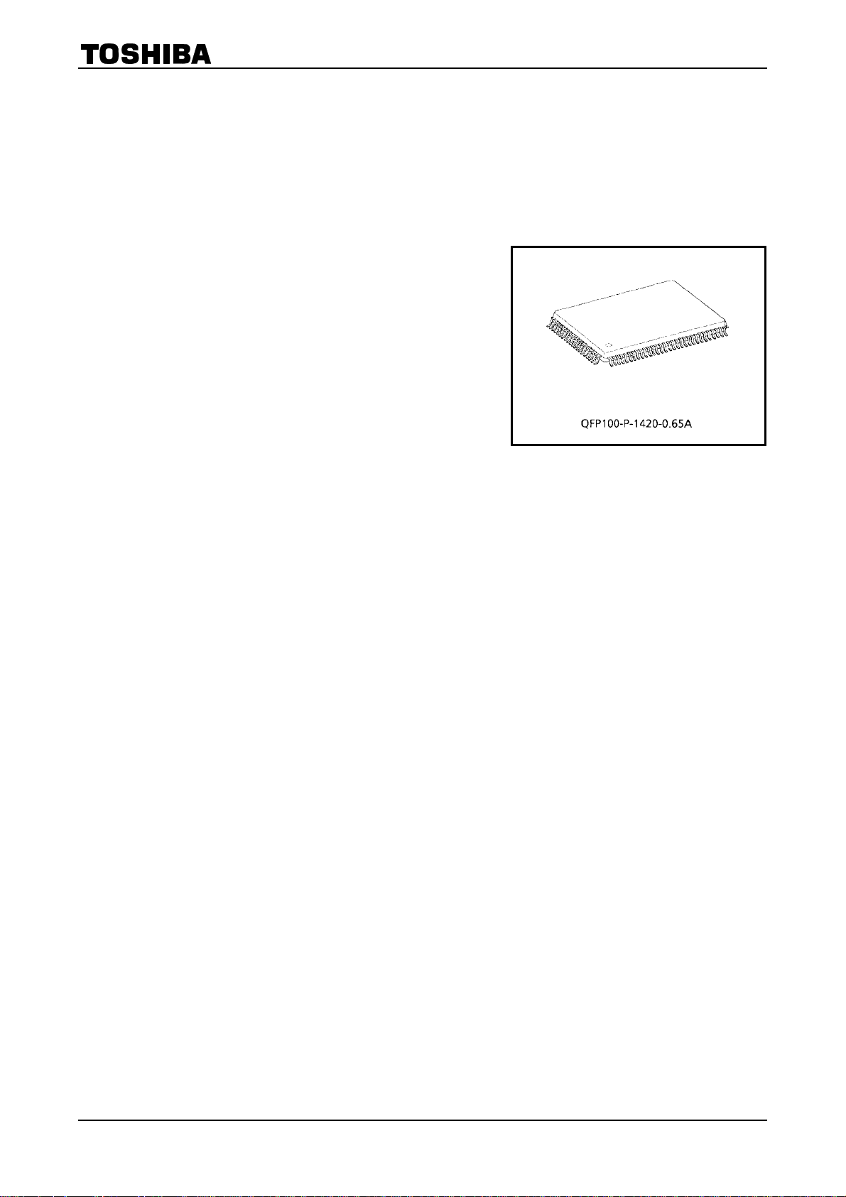
· 100 pin flat package.
TC9457F
2
2002-10-21
Page 3
TC9457F
2002-10-21
3
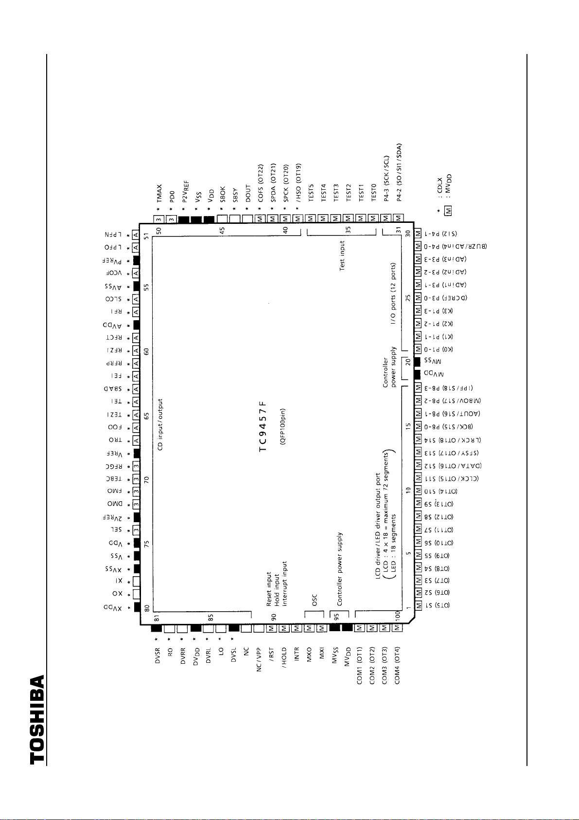
Pin Connection Diagram
Page 4
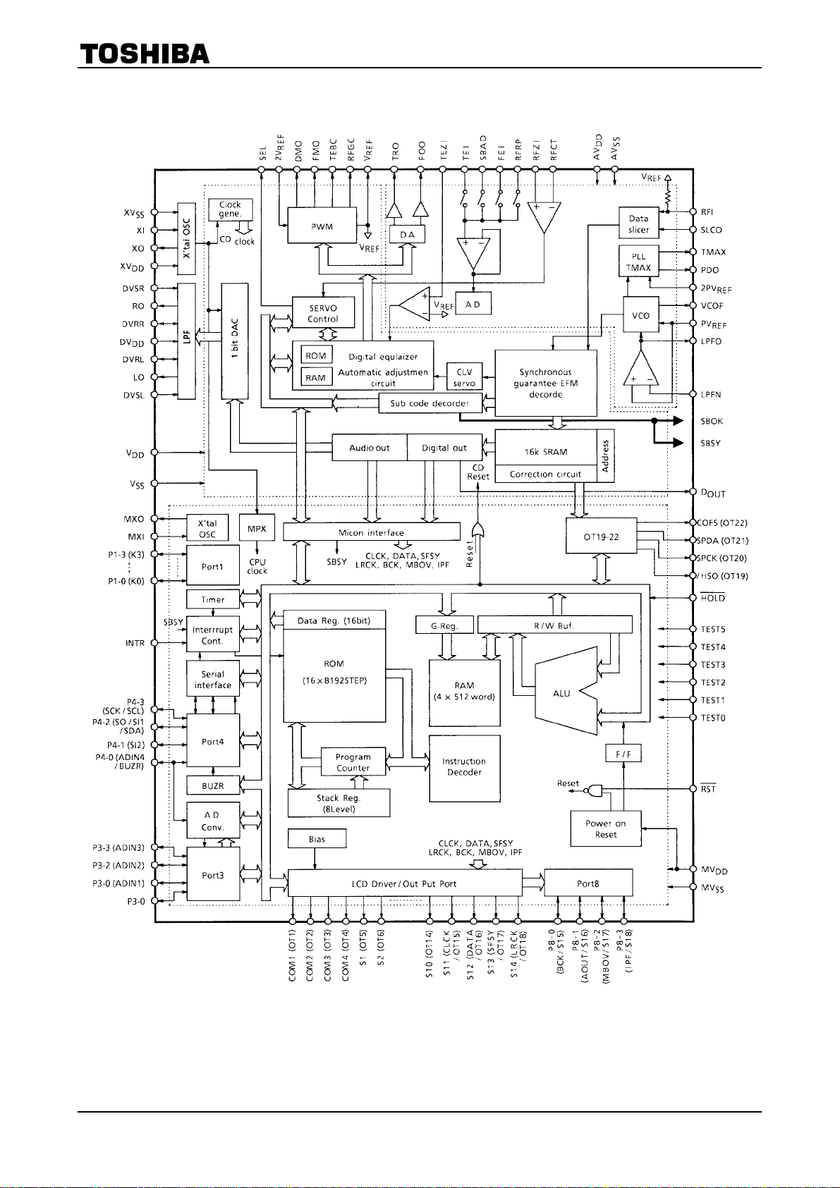
Block Diagram
TC9457F
4
2002-10-21
Page 5
Description Of Pin Function
Pin No. Symbol Pin Name Function And Operation Remarks
TC9457F
1~10
11
12
13
14
15
16
17
18
21~24
S1/OT5
~
S10/OT14
S11/OT15
/CLCK
S12/OT16
/DATA
S13/OT17
/SFSY
S14/OT18
/LRCK
S8-0/S15
/BCK
P8-1/S16
/AOUT
P8-2/S17
/MBOV
P8-3/S18
/IPF
P1-0~P1-3
/K0~K3
LCD segment
outputs
/Output ports
LCD segment
outputs
/Output ports
/CD signals
I/O ports
/LCD segment
outputs
/CD signals
I/O port 1
/Key input
ports
Segment signal outputs to the LCD panel.
Up to 72 segments in a matrix with COM1 to COM4 can
be displayed.
All of the S1 to S18 pins can be switched for output ports
by a program (Note 1). Also, the S15 to S18 pins each
can be switched for I/O ports individually. When set for I/O
ports, these pins become Nch open-drain outputs.
Furthermore, the S11 to S14 and the P8-0 to P8-3 pins
can be switched for use as CD signal (CLCK to IPF)
input/output pins by a program.
For CD signal output, set parameters OT for output and
LEDon = 1.
Furthermore, when set for output ports, the buffer
capability can be increased by setting the LEDon bit to 1,
so that it can be used as an LED driver. These pins
normally are used for LED segment outputs.
output ports can increment OT1 through OT18 by an
instruction, data in external RAM/ROM can be accessed
easily.
Note 1: After a system reset, the output port shared pins
4-bit CMOS I/O ports.
These ports can be set for input or output bit for bit by a
program.
These pins can be pulled up to V
program. Therefore, they can be used as key input pins.
Also, when they are set for I/O port input, a change of
state in this input can be used to clear the clock stop or
wait mode.
· CLCK : Subcodes P thru W data readout clock
input/output.
Selected between input and output by
a command.
· DATA : Subcodes P thru W data output.
· SFSY : Playback system frame sync
signal output.
· LRCK : Channel clock (44.1 kHz) output. It
outputs a low for L channel and a high
for R channel. Polarity can be inverted
by a command.
· BCK : Bit clock (1,4112 MHz) output.
· AOUT : Audio data output.
· MBOV : Buffer memory-over signal output.
It outputs a high when buffer overflows.
· IPF : Correction flag output. When AOUT is
C2 correction output, it outputs a high
indicating that
correction is impossible.
Since the
are set for LCD output and the I/O port shared
pins are set for I/O port input.
or down to GND by a
DD
―
―
―
―
―
―
―
―
―
―
5
2002-10-21
Page 6

TC9457F
Pin No. Symbol Pin Name Function And Operation Remarks
25
26~28
29
30
31
32
33~38
39~42
P3-0/DCREF
P3-1/ADIN1
~
P3-3/ADIN3
P4-0/ADIN4/
BUZR
P4-1/S12
P4-2/S0/SI1
/SDA
P4-3/SCK
/SCL
TEST0
~
TEST5
/HSO/OT19
SPCK/OT20
SPDA/OT21
COFS/OT22
I/O port 3
/AD analog
reference
voltage input
I/O port 3
/AD analog
voltage input
I/O port 4
/AD analog
voltage inputs
/Buzzer output
I/O port 4
/Serial data
input
/Serial data
input /output
/Serial clock
input /output
Test mode
control inputs
CD control
signal outputs
/output ports
5-bit CMOS I/O ports.
These ports can be set for input or output bit for bit by a
program.
The P3-0 to P4-0 pins serve dual purposes as analog
inputs for the internal 6-bit 4-channel AD converters.
The internal AD converters can complete conversion in 6
instruction cycles using a successive approximation
method. The required pins can be set for AD analog input
bit for bit by a program. P3-0 can be set for reference
voltage input, and the internal power supply (MV
be used for this reference voltage.
The P4-0 pin serves dual purposes as a buzzer output
pin.
The buzzer output can be selected from 8 frequencies,
0.625 to 3 kHz. Each selected frequency can be output in
one of four modes: continuous, single, 10 Hz intermittent,
and 10 Hz intermittent at 1 Hz interval.
Whether or not to use and how to control the AD converter
and buzzer all can be set by a program.
Note 2: If P3-0 is set for reference voltage input, note that
3-bit CMOS I/O ports.
These ports can be set for input or output bit for bit by a
program.
These pins serve dual purposes as input or output pins for
the serial interface circuit (SI0).
The SI0 is a 2-wire/3-wire compatible serial interface.
4 or 8 bits of serial data, beginning with the MSB or LSB,
are serially output from the SO/SDA pin at each clock
edge on the SCK/SCL pin, and the data on SI1 or SI2 pin
is serially input to the device. The serial clock (SCK/SCL)
allows selection between the internal (450/225/150/75
kHz) and external sources and a selection of the active
edge, rise or fall. Moreover, since the clock and data can
be output via Nch open-drain outputs, various device
controls and communication between controllers can be
greatly facilitated.
When an SI0 interrupt is enabled, an interrupt is
generated at completion of SI0 execution and the program
jumps to address 4. This is effective when high-speed
serial communication is desired.
All inputs to SI0 contain a Schmitt trigger circuit.
Whether or not to use SI0 and how to control it all can be
set by a program.
Test mode control input pins.
The test mode is selected when these pins are set high
and normal operation is selected when they are low.
These pins normally must be held low or left open (NC)
when used for this purpose. (Pulldown resistors are
built-in).
CD control output pins.
although normally in a high-impedance state, this
input during AD conversion becomes a 10 kΩ
load, typ. Therefore, pay careful attention to the
output impedance that is input to this pin.
) can
DD
· /HSO : Playback speed mode output.
High = normal speed;
Low = double speed.
· SPCK : Processor status signal readout
clock output (176.4 kHz)
· SPDA : Processor status signal output.
· COFS : Correction system frame clock output
(7.35 kHz).
These pins can be switched for output ports by a program.
―
―
―
―
43 DOUT Digital output pin. ―
44 SBSY
CD control
input/outputs
Subcode block sync output pin. It outputs a high at the S1
position when subcode sync is detected.
6
―
2002-10-21
Page 7

TC9457F
Pin No. Symbol Pin Name Function And Operation Remarks
45 SBOK
46, 75 VDD ―
47, 76 VSS
48 P2V
49 PDO
50 TMAX
51 LPFN Inverted input of low-pass filter amp. Analog input
52 LPFO Output of low-pass filter amp. Analog output
53 PVREF PLL block V
54 VCOF VCO filter pin. Analog output
55 AVSS Analog block ground pin. ―
56 SLCO DAC output pin for data slice level generation. Analog output
57 RFI RF signal input pin.
58 AVDD Analog block power supply pin. ―
59 RFCT RFRP signal center level input pin. Analog input (Zin = 50 kΩ)
60 RFZI RFRP zero-cross input pin. Analog input
61 RFRP RF ripple signal input pin. Analog input
62 FEI Focus error signal input pin.
63 SBAD Subbeam add signal input pin. Analog input
64 TEI
65 TEZI Tracking error zero-cross input pin. Analog input (Zin = 10 kΩ)
66 FOO Focus equalizer output pin.
67 TRO Tracking equalizer output pin.
68 V
69 RFGC
70 TEBC
71 FMO
72 DMO
73 2V
PLL block-2 V
REF
CD control
input/outputs
Analog reference power supply pin. ―
REF
REF
Subcode Q data CRCC determination result output pin. It
outputs a high when CRCC check is found OK.
CD unit's digital block power supply pins.
Normally, apply 5 V to VDD.
When not using a CD (CD off), this power supply can be
turned off, with only the controller power supply kept
active, so that the controller alone is operating. In this
case, the CDoff bit must be set to 1. When this bit is set to
1, pins 11 through 18 and pins 39 through 42 all are
changed for output ports if they have been set for CD
control signal input/output pins.
pin. ―
REF
This pin outputs a phase error between EFM and PLCK
signals.
TMAX detection result output pin. Selected by command
bit TMPS.
Longer than preset period : Outputs P2V
Shorter than preset period : Low level (V
Within preset period : High impedance.
pin. ―
REF
Tracking error input pin. This input is read when tracking
servo is on.
RF amplitude adjusting control signal output pin. It outputs
3-level PWM signals. (PWM carrier = 88.2 kHz)
Tracking balance control signal output pin. It outputs
3-level PWM signals.
(PWM carrier = 88.2 kHz)
Focus equalizer output pin. It outputs 3-level PWM
signals.
(PWM carrier = 88.2 kHz)
Disc equalizer output pin. It outputs 3-level PWM signals.
(PWM carrier = DSP block 88.2 kHz, synchronized to
PXO)
Analog reference power supply pin. (2 × V
.
REF
).
SS
) ―
REF
―
―
―
―
Analog input
(Zin : command select)
Analog input
Analog input
Analog output
to AVSS)
(2V
REF
Analog output
to AVSS)
(2V
REF
―
―
―
―
7
2002-10-21
Page 8

TC9457F
Pin No. Symbol Pin Name Function And Operation Remarks
74 SEL
77 XVSS ―
80 XVDD
78 XI ―
79 XO
81 DVSR R-channel DA converter unit ground pin. ―
82 RO R-channel data forward output pin. ―
83 DVRR R-channel reference voltage pin. ―
84 DVDD DA converter unit power supply pin. ―
85 DVRL L-channel reference voltage pin. ―
86 LO L-channel data forward output pin. ―
87 DVSL L-channel DA converter unit ground pin. ―
88, 89 NC
90 RESET Reset input
91 HOLD
CD control
input/outputs
Hold mode
control input
APC circuit on/off signal output pin. When laser is on, this
pin goes to a high-impedance state when UHS = low and
outputs a high when UHS = high.
CD's crystal oscillator power supply pins. Normally,
connect these pins to the power supply lines that are used
in common for the V
CD's crystal oscillator input/output pins. Normally, connect
16.9344 MHz here. This clock is used as the system clock
for the CD. After a system reset, it also is used as the
system clock on the controller side. Therefore, all of the
CD power supplies must be fed with power after a reset.
NC pins. Normally, connect these pins to ground or leave
them open. Pin 89 serves dual purposes as the V
2
an E
PROM product. Therefore, when this pin is left open,
it can be shared with an E
Device's system reset signal input pin.
The device remains reset while
when
RESET is released back high, the CD unit
becomes operational and the program starts from address
0. Normally, a system reset is asserted when a voltage of
2.7 V or more is applied to V
(power-on reset). Therefore, this pin must be pulled high
when used for this purpose.
This pin is used to input a signal that requests or clears
the hold mode.
Normally, use this pin for CD mode select signal input or
battery detection signal input.
There are two hold modes : clock stop mode (crystal
oscillator turned off) and a wait mode (CPU stopped).
These modes are entered by executing the CKSTP and
WAIT instructions, respectively.
The clock stop mode can be requested by a programmed
input: low level detection on
execution, and can be cleared by detecting a high on the
HOLD pin or a change of state in its input signal. When
the CKSTP instruction is executed, the clock generator
and the CPU stop operating and the device is placed in a
memory backup state. During this state, the device's
current consumption is reduced to 1µA or less. At the
same time, the display output and CMOS output ports are
automatically set low, and the Nch open-drain outputs are
turned off.
The wait mode is executed regardless of the input state
on the
HOLD pin, with the device's current consumption
reduced. In this mode, the user can choose to keep only
the crystal oscillator operating or have the CPU paused by
programming.
If the former is selected, all display outputs are set low
and other pins retain their state ; if the latter is selected, all
states are retained except that the CPU is temporarily
stopped.
This mode is cleared by a change of state in the
input.
and VSS pins.
DD
2
PROM product.
DD
HOLD pin or forced
pin of
pp
RESET is held low and
when it is at 0 V
HOLD
―
―
―
―
―
―
8
2002-10-21
Page 9

TC9457F
Pin No. Symbol Pin Name Function And Operation Remarks
External interrupt input pin.
When the interrupt facility is enabled and a pulse of 1.11
to 2.22 µs in duration is applied to this pin, an interrupt is
generated and the program jumps to address 1.
92 INTR
93 MXO ―
94 MXI
External
interrupt input
Controller's
crystal
oscillator pins
Input logic and the active edge (rise or fall) can be
selected for each interrupt input.
Also, the internal 8-bit timer clock can be chosen for this
interrupt input, in which case it is possible to count pulses
or generate an interrupt at a given pulse count
(address 3).
Since this pin is a Schmitt trigger type, it can be used as
an input port for receiving remote control signals, etc.
Crystal oscillator pins for the controller.
The oscillator clock is used as the timebase for the clock
facility or as the controller's system clock. Connect a
4.5 MHz or 75 kHz crystal resonator to the MXO and MXI
pins. Since these pins do not contain internal feedback
resistors, etc, an amp resistor or output resistor must be
added external to the chip.
· 75 kHz··· ROUT = 100 kΩ, Rf = 10 MΩ
Ci = Co = 15 pF (typ.)
· 4.5 MHz··· ROUT = 0 Ω, Rf = 1 MΩ
Ci = Co = 15 pF (typ.)
When using the clock generated by the CD unit's crystal
oscillator for clocking the entire device operation, fix the
MXI pin to the GND level.
Oscillation is stopped by executing a CKSTP instruction.
Select the crystal oscillator and control its operation by a
program.
Note 3: When after turning on the CD unit's power supply,
the controller system clock is switched from the
crystal oscillator on the controller side to that on
the CD side, provide an allowance time of several
10 ms for the CD unit's crystal oscillator to
stabilize after it is powered on. This is necessary
to prevent the controller from operating erratically.
―
―
Power supply pins.
Normally, apply a voltage of 4.5 to 5.5 V to V
19, 96 MVDD ―
Controller unit
power supply
pins
20, 95 MVSS
97 COM1/OT1 ―
98 COM2/OT2 ―
99 COM3/OT3 ―
100 COM4/OT4
LCD common
outputs
/Output ports
In a backup state (when the CKSTP instruction executed),
the device's current consumption is reduced to 1 µA or
less, allowing for the supply voltage to be lowered to
2.0 V.
The device is reset and the program starts from address 0
when a voltage of 2.7 V or more is applied to this pin
when it is at 0 V (power-on reset).
Note 4: For reason of this power-on reset, make sure the
device's power supply rise time is between 10 to
100 ms.
Common signal outputs to the LCD panel. Up to 72
segments in a matrix with S1 to S18 can be displayed.
Three voltage levels MV
are output for 83 Hz period at 2 ms intervals.
After a system reset and after deassertion of a clock stop
instruction, the V
bit is set to 0 before common signals are output.
These pins can be switched for output ports by a program
(Note1). In this case, the buffer capacity can be increased
by setting the LEDon bit to 1, so that it can be used as an
LED driver. These four pins normally are used for LED
digit outputs.
EE
, VEE (1/2 MVDD), and GND
DD
voltage is output and the DISP OFF
DD
.
―
―
9
2002-10-21
Page 10

TC9457F
Maximum Ratings
Characteristics Symbol Rating Unit
Power supply voltage VDD −0.3~6.0 V
Input voltage VIN −0.3~VDD + 0.3 V
Power dissipation PD 1400 mW
Operating temperature T
Storage temperature T
(Ta = 25°C)
−40~85 °C
opr
−65~150 °C
stg
Electrical Characteristics
2V
= P2V
REF
MVDD
Operating supply voltage
Memory retention voltage range MVHD ―
Operating supply current
Memory retention current MIHD ―
Crystal oscillation frequency
Crystal oscillation start time tst ―
(CPU unit power supply)
= 4.2 V, V
REF
Characteristics Symbol
(Ta = 25°C, VDD = MVDD = AVDD = DVDD = XVDD = 5 V,
REF
= PV
= 2.1 V, unless otherwise specified)
REF
Test
Circuit
MV
―
DD1
MV
―
DD2
―
MV
DD3
MV
―
DD1
MV
―
DD2
MV
―
DD3
―
MV
DD4
f MXT1 ―
f MXT2
―
When CPU and CD operating.
However,
MV
When CPU operating
(CD powered off, 4.5 MHz
crystal connected) (Note 5)
When CPU operating (CD
powered off, 75 kHz crystal
connected) (Note 5)
When crystal oscillator stopped
(CKSTP instruction executed)
(Note 5)
When CPU operating
(XI = 16.9344 MHz crystal
connected)
When CPU operating(MXI =
4.5 MHz crystal connected)
When CPU operating (MXI =
75 kHz crystal connected)
Standby mode (only crystal
oscillating, 4.5 MHz or 75 kHz
crystal connected)
When crystal oscillator stopped
(CKSTP instruction executed)
Rf = 1 MΩ, Rout = 0 Ω,
Ci = Co = 30 pF (Note 5, 6)
Rf = 10 MΩ, Rout = 100 kΩ,
Ci = Co = 15 pF,
MV
Crystal oscillation fmxt = 75
kHz
Test Condition Min Typ. Max Unit
≥ VDD (Note 5)
DD
= 2.7~5.5 V (Note 5, 6)
DD
4.5 5.0 5.5
4.5 5.0 5.5
2.7 5.0 5.5
2.0 ~ 5.5 V
― 1.0 2.0
― 2.0 4.0
― 0.75 2.0
― 0.5 15
― 0.1 1.0 µA
― 4.5 ― MHz
― 75 ― kHz
― ― 1.0 s
V
mA
Note 5: Guaranteed at V
DD
= MV
= 4.5 to 5.5 V and Ta = −40 to 85°C
DD
Note 6: Consider the crystal resonator used in your system when determining constants, etc.
10
2002-10-21
Page 11
TC9457F
VDD
(CD unit power supply)
Characteristics Symbol
Operating supply voltage V
Operating supply current I
Crystal oscillation frequency f
Note 5: Guaranteed at V
DD
= MV
Test
Circuit
― MV
DD
―
DD
―
XT
= 4.5 to 5.5 V and Ta = −40 to 85°C
DD
When 16.9344 MHz crystal
connected
Rout = 0 Ω, Ci = Co = 15 pF
(Note 5, 6)
Test Condition Min Typ. Max Unit
≥ VDD (Note 5) 4.5 5.0 5.5 V
DD
― 50 60 mA
― 16.9344 ― MHz
Note 6: Consider the crystal resonator used in your system when determining constants, etc.
LCD Common Output
Characteristics Symbol
High level
Output current
Low level
Output voltage 1/2 level VBS ― Nonloaded (when LCD output) 2.1 2.3 2.5 V
Segment Output
(COM1/OT1 to COM4/OT4)
Test
Circuit
I
―
OH2
I
―
OH5
I
―
OL2
―
I
OL5
(S1/OT4 to S10/OT14, S11/OT15 to P8-0/S14 to P8-3/S18)
Test Condition Min Typ. Max Unit
= 4.5 V (When LCD
V
OH
output, settings OT output,
LEDon = 0)
= 4.5 V (Settings OT
V
OH
output, LEDon = 1)
= 0.5 V (When LCD
V
OL
output, settings OT output,
LEDon = 0)
= 0.5 V (Settings OT
V
OL
output, LEDon = 1)
−0.1 −0.2 ―
−20 −40 ―
0.1 0.2 ―
4 10 ―
mA
Characteristics Symbol
I
OH1
High level
I
―
OH4
Output current
I
―
OL1
Low level
―
I
OL5
Input leakage current ILI ―
High level VIH ― (P8-0 to P8-3)
Input voltage
― (P8-0 to P8-3) 0 ~
Low level
V
IL
Test
Circuit
VOH = 4.5 V
(When LCD output, settings
―
OT output, LEDon = 0)
V
(Settings OT output,
LEDon = 1, I/O port)
V
(When LCD output, settings
OT output, LEDon = 0)
V
(Settings OT output,
LEDon = 1, I/O port)
V
(P8-0 to P8-3)
Test Condition Min Typ. Max Unit
= 4.5 V
OH
= 0.5 V
OL
= 0.5 V
OL
= 5.0 V, VIL = 0 V
IH
−0.05 −0.1 ―
−2 −4 ―
mA
0.05 0.1 ―
5 10 ―
― ― ±1.0 µA
MV
DD
× 0.8
~ MV
MV
× 0.2
DD
V
DD
11
2002-10-21
Page 12

TC9457F
I/O Ports
Output current
Input leakage current ILI ― VIH = 5.0 V, VIL = 0 V ― ― ±1.0 µA
Input voltage
Input pullup/down resistance R
(P1-0 to P4-3)
Characteristics Symbol
Test
Circuit
High level I
Low level
High level VIH ― ―
Low level V
― VOH = 4.5 V −1 −2 ―
OH3
I
―
OL3
I
― VOL = 0.5 V (P4-1, 2, 3 pin) 4 10 ―
OL5
― ― 0 ~
IL
―
IN1
V
(exclude P4-1, 2, 3 pin)
(P1-0 to P1-3) When pulldown,
pullup are set.
Test Condition Min Typ. Max Unit
= 0.5 V
OL
1.5 3.0 ―
MV
DD
× 0.8
25 50 120 kΩ
~ MV
MV
× 0.2
DD
DD
HOLD
Input leakage current ILI ― VIH = 5.0 V, V
Input voltage
, INTR Input Port,
Characteristics Symbol
High level V
Low level V
RESET
Input
Test
Circuit
― ―
IH3
― ― 0 ~
IL3
Test Condition Min Typ. Max Unit
= 0 V ― ― ±1.0 µA
IL
MV
DD
× 0.8
~ MV
MV
× 0.2
DD
DD
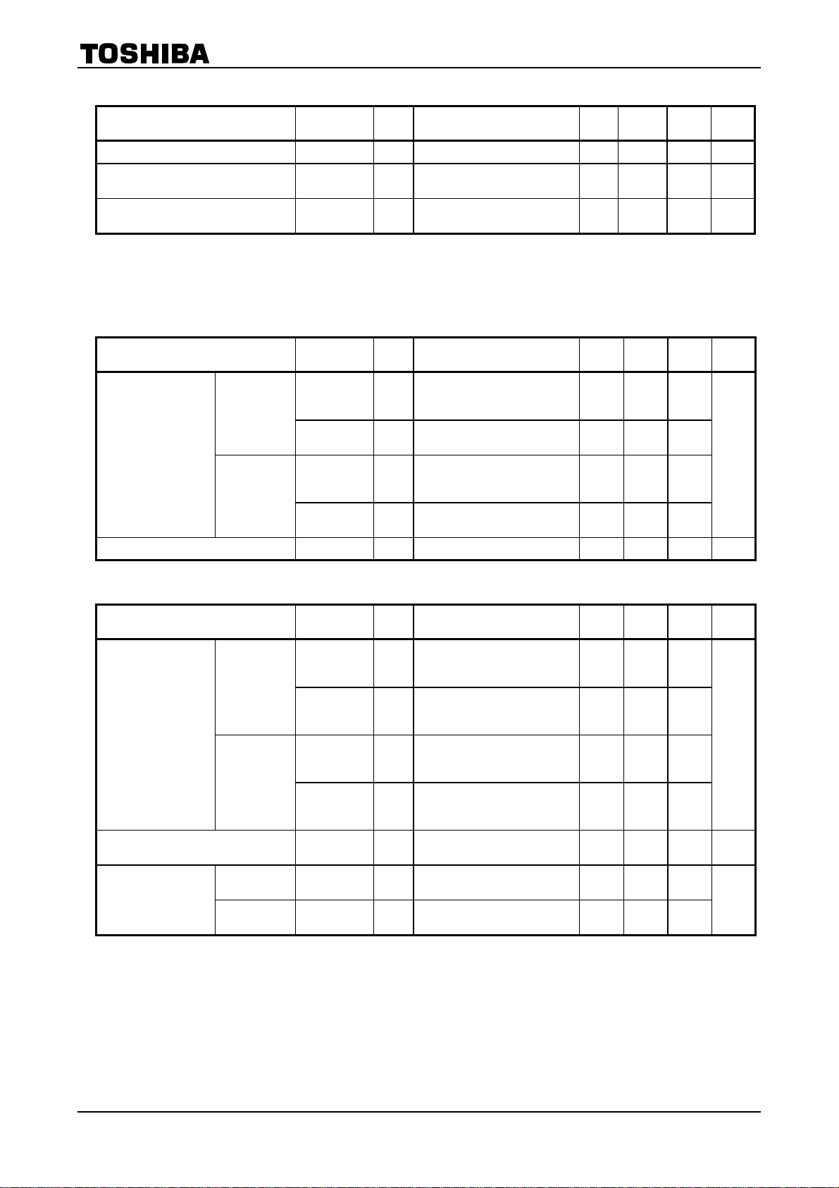
A/D Converter
Characteristics Symbol
Analog input voltage range VAD ― ADIN to AD
Resolution V
Overall conversion error ― ― ― ― ±0.5 ±4.0 LSB
Analog input leakage ILI ―
(AD
IN1
to AD
IN4
)
Test
Circuit
― ― ― 6 ― bit
RES
V
(AD
Test Condition Min Typ. Max Unit
0 ~ MV
IN4
= 5.0 V, V
IH
IN1
to AD
IN4
IL
= 0 V
)
― ― ±1.0 µA
DD
DATA, SFSY, LRCK, BCK, AOUT, MBOV, IPF Outputs and CLCK Input/Output
mA
V
V
V
Characteristics Symbol
High level I
Output current
Low level I
Input leakage current ILI ―
High level VIH ― (CLCK)
Input voltage
Low level V
―
OH4
―
OL5
― (CLCK) 0 ~
IL
Test
Circuit
= 4.5 V
V
OH
(Settings OT for output,
LEDon = 0)
= 0.5 V
V
OL
(Settings OT for output,
LEDon = 0)
= 5.0 V, VIL = 0 V
V
IH
(CLCK)
12
Test Condition Min Typ. Max Unit
−2.0 −4.0 ―
mA
5 10 ―
― ― ±1.0 µA
MV
DD
× 0.8
~ MV
MV
× 0.2
DD
V
DD
2002-10-21
Page 13

DOUT, SBSY, SBOK, SEL, HSO, SPCK, SPDA, COFS Outputs
TC9457F
Characteristics Symbol
Output voltage
High level I
Low level I
OH4
OL4
Test
Circuit
― VOH = 4.5 V −2 −4 ―
― VOL = 0.5 V 2 4 ―
Test Condition Min Typ. Max Unit
PDO, TMAX, RFGC, TEBC, DMO Outputs
Characteristics Symbol
Output voltage
High level I
Low level I
Propagation Delay Time
Characteristics Symbol
Propagation
delay time
High level t
Low level t
OH6
OL4
(AOUT, SPDA, DATA, SBSY, SBOK)
pLH
pHL
Test
Circuit
― VOH = 3.8 V −1.0 −2.0 ―
― VOL = 0.5 V 3.0 6.0 ―
Test
Circuit
― ― ― 10 ―
― ― ― 10 ―
Test Condition Min Typ. Max Unit
Test Condition Min Typ. Max Unit
1bit DA Converter
Characteristics Symbol
Noise distortion THD + N ―
S/N ratio S/N ― ― 90 98 ― dB
Dynamic range DR ―
Crosstalk CT ―
Analog output level DACout ―
Other
Test
Circuit
1 kHz sine-wave,
full-scale input
1 kHz sine-wave,
−60 dB input conversion
1 kHz sine-wave,
full-scale input
1 kHz sine-wave,
full-scale input
Test Condition Min Typ. Max Unit
― −85 −78 dB
85 90 ― dB
― −90 −85 dB
1200 1250 1300 mVrms
mA
mA
ns
Characteristics Symbol
Input pulldown resistance R
XI amp feedback resistance R
Test
Circuit
― (TEST0 to TEST5) ― 10 ― kΩ
IN2
― (XI−XO) 1 2 4 MΩ
fXT
13
Test Condition Min Typ. Max Unit
2002-10-21
Page 14

Package Dimensions
TC9457F
Weight: 1.6 g (typ.)
14
2002-10-21
Page 15

TC9457F
A
RESTRICTIONS ON PRODUCT USE
· TOSHIBA is continually working to improve the quality and reliability of its products. Nevertheless, semiconductor
devices in general can malfunction or fail due to their inherent electrical sensitivity and vulnerability to physical
stress. It is the responsibility of the buyer, when utilizing TOSHIBA products, to comply with the standards of
safety in making a safe design for the entire system, and to avoid situations in which a malfunction or failure of
such TOSHIBA products could cause loss of human life, bodily injury or damage to property.
In developing your designs, please ensure that TOSHIBA products are used within specified operating ranges as
set forth in the most recent TOSHIBA products specifications. Also, please keep in mind the precautions and
conditions set forth in the “Handling Guide for Semiconductor Devices,” or “TOSHIBA Semiconductor Reliability
Handbook” etc..
· The TOSHIBA products listed in this document are intended for usage in general electronics applications
(computer, personal equipment, office equipment, measuring equipment, industrial robotics, domestic appliances,
etc.). These TOSHIBA products are neither intended nor warranted for usage in equipment that requires
extraordinarily high quality and/or reliability or a malfunction or failure of which may cause loss of human life or
bodily injury (“Unintended Usage”). Unintended Usage include atomic energy control instruments, airplane or
spaceship instruments, transportation instruments, traffic signal instruments, combustion control instruments,
medical instruments, all types of safety devices, etc.. Unintended Usage of TOSHIBA products listed in this
document shall be made at the customer’s own risk.
· The products described in this document are subject to the foreign exchange and foreign trade laws.
· The information contained herein is presented only as a guide for the applications of our products. No
responsibility is assumed by TOSHIBA CORPORATION for any infringements of intellectual property or other
rights of the third parties which may result from its use. No license is granted by implication or otherwise under
any intellectual property or other rights of TOSHIBA CORPORATION or others.
000707EB
· The information contained herein is subject to change without notice.
15
2002-10-21
Page 16

This datasheet has been download from:
www.datasheetcatalog.com
Datasheets for electronics components.
 Loading...