

Page 1

SERVICE MANUAL
DOCUMENT CREATED IN JAPAN, SEPT., 2005
PORTABLE DVD PLAYER
SD-P1800
FILE NO. 810-200575
Rev.00
DIGITAL VIDEO
(USA)
Sep., 2005
Page 2
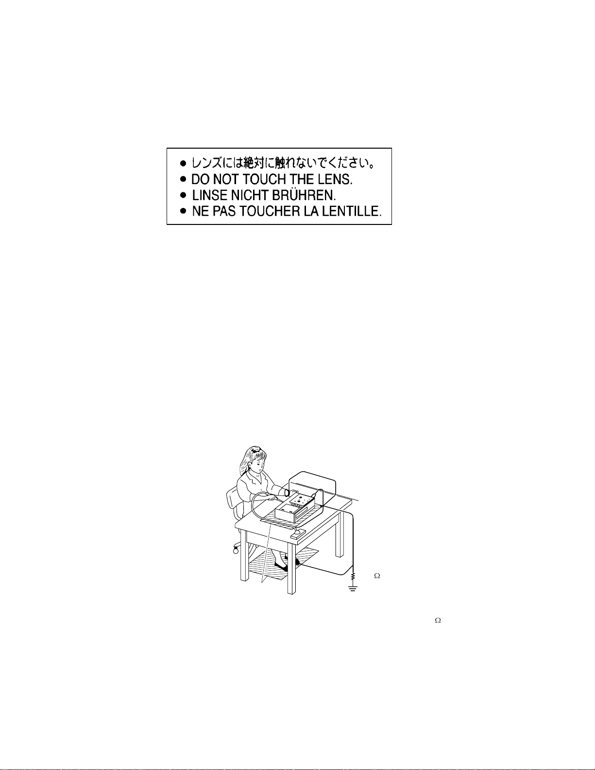
LASERBEAMCAUTIONLABEL
Whenthepowersupplyisbeingturnedon,youmaynotremovethislasercautionslabel.Ifitremoves,radiationoflaser
maybereceived.
PREPARATIONOFSERVICING
PickupHeadconsistsofalaserdiodethatisverysusceptibletoexternalstaticelectricity.
Althoughitoperatesproperlyafterreplacement,ifitwassubjecttoelectrostaticdischargeduringreplacement,
itslifemightbeshortened.Whenreplacing,useaconductivemat,solderingironwithgroundwire,etc.to
protectthelaserdiode
Andalso,theLSIandICaresameasabove.
fromdamagebystaticelectricity.
Solderingiron
withgroundwire
orceramictype
Conductivemat
Groundconductive
wriststrapforbody.
1M
Thegroundresistance
betweenthegroundline
andthegroundislessthan10
Page 3
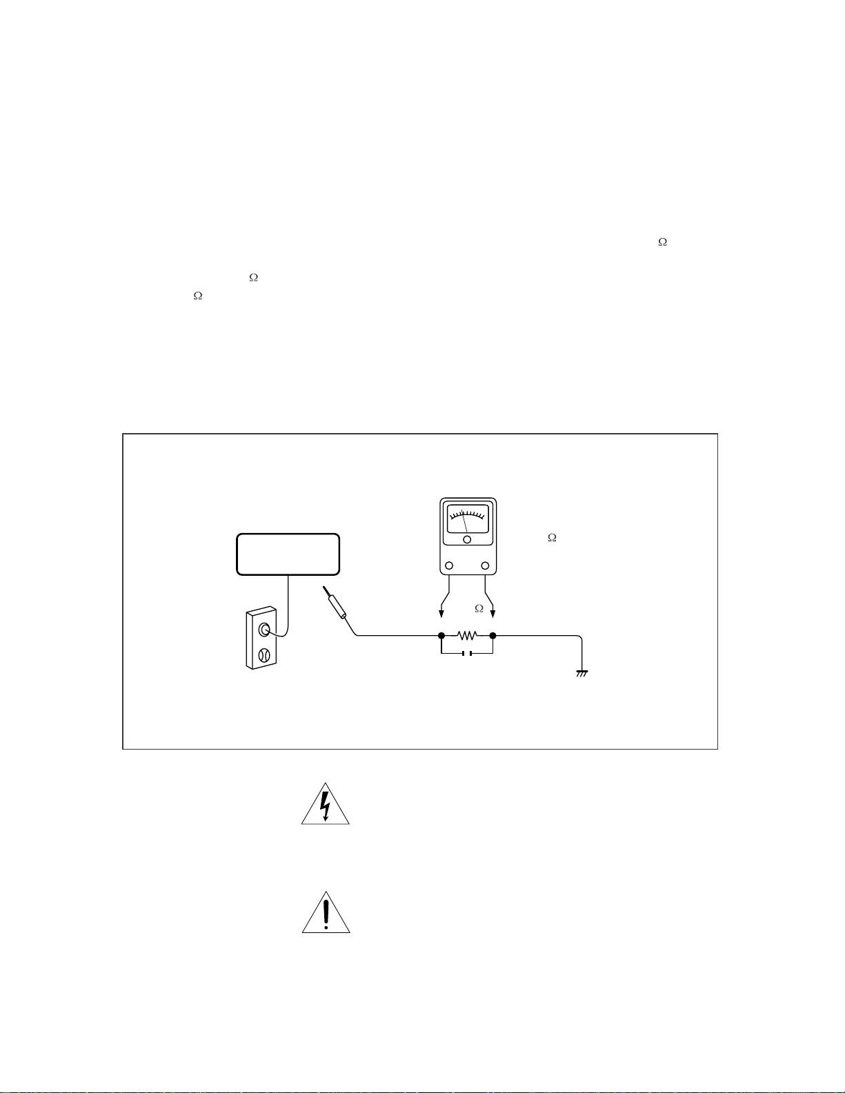
SAFTY NOTICE
LEAKAGE CURRENT CHECK
SAFTY PRECAUTIONS
Plug the AC line cord directly into a 120V AC outlet (do
not use an isolation transformer for this check). Use an
AC voltmeter, having 5000 per volt or more sensitivity.
Connect a 1500 10W resistor,paralleled by a 0.15uF
150V AC capacitor between a known good earth ground
(water pipe, conduit, etc.) and all exposed metal parts of
cabinet (antennas, handle bracket, metal cabinet
screwheads, metal overlays, control shafts, etc.).
READING SHOULD NOT EXCEED 0.3V
DVD VIDEO PLAYER
Measure the AC voltage across the 1500 resistor.
The test must be conducted with the AC switch on and
then repeated with the AC switch off. The AC voltage
indicated by the meter may not exceed 0.3V.A reading
exceeding 0.3V indicates that a dangerous potential
exists, the fault must be located and corrected.
Repeat the above test with the DVD VIDEO PLAYER
power plug reversed.
NEVER RETURN A DVD VIDEO PLAYER TO THE
CUSTOMER WITHOUT TAKING NECESSARY
CORRECTIVE ACTION.
AC VOLTMETER
(5000 per volt
or more sensitivity)
Good earth ground
1500
10W
such as a water pipe,
conduit, etc.
AC OUTLET
0.15uF 150V AC
Test all exposed metal.
Voltmeter Hook-up for Leakage Current Check
The lightning flash with arrowhead symbol, within an
equilateral triangle, is intended to alert the user to the
presence of uninsulated "dangerous voltage" within the
product's enclosure that may be of sufficient magnitude to
constitute a risk of electric shock to persons.
The exclamation point within an equilateral triangle is
intended to alert the user to the presence of important
operating and maintenance (servicing) instructions in the
literature accompanying the appliance.
Page 4
LCD
1
2
1 2 3 4 5 6 7 8 91011121314151617181920212223242526272829
TFT+17VNC3.3V
TFT GND
TFT-13VNCSTV1
V/D
CKV
OEV
OEV
OEV
STV2
VCOMS
TFT GND
VEE
STH2
L/R
CPH1
CPH1
CPH1
MODE
3.3V
OEH
LCD B
LCD G
1
2
1 2 3 4 5 6 7 8 91011121314151617181920212223242526272829
LCD R
VBS
30
STH1
VCOMS
30
BATTERY
123
BATT+TSGND
123
XS102
4
GND
4
XS5
XS6
1 2 3 4 5 6 7 8 9101112131415
HVHVBRIGHT
TFT on/off
GND
GND
SPR+
SPR-
SPL+
SPL-
GND
TFT+17V
GND
TFT-13V
GND
1 2 3 4 5 6 7 8 9101112131415
JS3
XS2
XS1
1 2 3 4 5 6 7 8 910111213141516171819
VCOMS
GND
TFT5V
TFT3.3V
GND
LCD G
LCD B
LCD R
GND
L/R
V/D
STV1
STV2
OEV
CKV
OEH
STH1
STH2
GND
1 2 3 4 5 6 7 8 910111213141516171819
JS5
MAIN PCB
INVERTER PCB
20
CPH1
20
XS1
1 2 3 4 5 6 7 8 91011121314151617181920212223
NC
DVDVCC
V20
GNDFE
CD/DVD SW
RFCDBA
1 2 3 4 5 6 7 8 91011121314151617181920212223
CDMD
DVDMDMDCDLD
GND
DVDLDNCAVCC
FCS-
TRK+
TRK-
24
FCS+
24
XS008
1 2 3 4 5
SP-
SP+
SL+
SL-
1 2 3 4 5
6
GND
LIMIT
6
1234567
KEYIN3
1234567
MECHANISM
KEYIN2
KEYIN1
KEYIN0
XS101
8
KEYOUT0
KEYOUT1
KEYOUT2
KEYOUT3
8
FUNCTION BUTTON PCB
Page 5
OSCILLATOR
OZ9930
DC 9V
HIGH VOLTAGE ASS'Y
TFT MONITOR
VIDEO OUT
COAXIAL OUT
AUDIO OUT
AUDIO AMP
(AZ4558)
PHONE OUT
SPEAKER LOUT
SPEAKER ROUT
SPEAKER AMP
TPA6011
27MHz
27MHz
27MHz
74HCU04
64M SDRAM
HY57V641620HGT-7
UPD5500
+5V
+3.3V
+1.8V
L
TFT POWER
+3.3V +5V +2.5V +16V -13V
L
R
AUDIO D/A
(PCM1753)
AUDIO +5V
R
AUDIO +/-5V
BATTERY
+5V
(VG202C)
(TPC8207)
(BQ2057C)
8M FlashROM
MX26LV800BTC-55
RF AMP & SERVO & DVD PROCESSOR
MPEG-2 DECODER & VIDEO ENCODER
MT1389SE
TC4W53
DV23(HD80)
OVERALL BLOCK DIAGRAM
PU mechanism
+5V
DRIVER +5V
DRIVER
(BA5888FP)
AC
110~240V
50/60Hz
DC / DC
Adapter
DC IN +9V
Page 6

1. Troubleshooting
1. No power when turned on.
2. The initial screen is not displayed on the LCD.
3. The DVD drive does not work.
4. The operation of the DVD player stops at initializing display.
5. Image output stops during the operation.
6. No sound or abnormal sound comes out from the speakers in the DVD player.
7. No image or sound comes out from the external output.
8. No sound comes out from the headphones.
9. No image or sound is output by external input.
10. The DVD drive does not operate with the battery.
1.1 No power when turned on.
When the power is turned on, and if the LED on the front panel does not light green, check
the following items and repair the defective parts.
(1) Check the power supply cable
If the cable is not the supplied one, replace it with the supplied cable and turn on the
power again.
If the power supply cable is good, the AC adapter may be defective.
If the LED does not light after replacing, check the following items.
(2) Check the AC adapter
If the AC adapter is not the supplied one, replace it with the supplied AC adapter and
turn on the power.
If the AC adapter is good, the main board may be defective.
If the LED does not light after replacing, check the following items.
(3) Replace the main board
Page 7

1.2 The initial screen is not displayed on the LCD.
If the initial screen is not displayed on the LCD, check the following items.
(1) Check the LED on the front
If the LED does not light, proceed to 1.1.
(2) Check the backlight
If the backlight does not light up, separate the DVD player into top assembly and
bottom assembly, and check the connector harness, and check the connectors for
defects.
If the connector harness is broken:
Replace the broken harness.
If the connector harness is not broken:
Remove the LCD cover and plate of the LCD unit and check the following:
zCheck the connector of the FL harness, replace the FL inverter or the LCD.
zIf the connectors are good, replace the FL inverter or the LCD.
(3) Check the lighting of LCD
If the LCD does not light, separate the DVD player into the top assembly and bottom
assembly, and check the LCD harness, and check the connectors on the main board.
If the connector is broken:
Replace the LCD harness or the main board.
If the connector is not broken:
Remove the LCD cover and plate of the LCD unit, and check the connection to the
harness of the LCD unit.
zIf a bad connection is found.
Connect the LCD harness to the LCD unit.
zOther than the above
Replace the LCD unit or the main board.
Page 8

1.3 The DVD drive does not work.
When the DVD drive does not work after the power is turned on, check the following items
and repair or replace the defective parts.
(1) Press the DISC cover switch and turn on the power. Then check whether or not
the optical pick-up lens of the DVD drive lights.
CAUTION: Visible laser radiation when open and interlock defeated. Do not stare into
Laser beam.
The optical pick-up lens lights dim:
It is caused by deterioration of the optical pick-up lens. Replace the DVD drive.
The optical pick-up lens does not light:
Check the connectors of the DVD-FFC. Also check the connection to the main
board and to the DVD drive.
zLoose connection is found.
Repair the connection, and then check the operation of the DVD drive again.
zThe DVD-FFC is broken.
Replace the DVD drive.
zOther than the above.
Replace the DVD drive or the main board.
(2) Insert a DVD disk and turn on the power
The DVD drive does not work:
The motor of the DVD drive or the main board is defective. Replace the DVD drive
or the main board.
The DVD drive works but the initializing operation of the optical pick-up lens
does not start (the optical pick-up lens operates twice), or abnormal noise
sound:
The DVD drive is defective. Replace the DVD drive.
1.4 The operation of the DVD player stops at initializing display.
If the DVD player does not work after the initializing screen is displayed, check the
indication on the screen. Then repair the defect according to it.
(1) Insert a DVD disk and close the DISC cover, and turn on the power. Then check
the LCD screen or use an external display.
zThe message “loading” is not displayed or the operation stops at the
message “Loading”.
Since the DVD drive or the main board is defective, check in the following order:
1) DVD drive
2) Main board
zThe message “CHECK DISK” is displayed.
Check the DVD disk for fingerprints, dirt, etc.
If the DVD disk is OK, then check the following items:
1) Check the DVD-FFC
If a loose connection, repair the connection.
If it is damaged, replace the DVD drive.
2) Other than above
For other cases, replace the unit in the following order:
zDVD drive (defective optical pick-up)
zMain board
Page 9

1.5 Image output stops during the operation.
If the image output from the media in the DVD player stops during the operation, replace
the DVD drive.
1.6 No sound or abnormal sound comes out from the speakers in the DVD player.
If no sound comes out from the speakers in the DVD player, check the following:
(1) Check for moving images on the LCD screen
Check whether or not the move of image stops in halfway. If it stops, replace the DVD
drive.
(2) Check the operation of the DVD driver.
Check whether or not the DVD drive works. If it stops, replace the DVD drive.
(3) Check the connection of the speakers in the DVD player.
Separate the DVD player into the top assembly and bottom assembly, and then check
the connections of the speaker harnesses to the inverter board and the inverter board
to the main board. If the connection is loose, repair connection. If the connector has
been connected firmly, replace the main board or speaker.
1.7 No image or sound comes out from the external output
If any image or sound is output from the TV connected by the external cable, replace the
main board.
NOTE: Before this test, make sure the drive works.
1.8 No sound comes out from the headphones.
If no sound comes out from the headphones, replace the main board.
1.9 No image or sound is output by the external input.
If any image or sound is output by external input, replace the main board.
1.10 The DVD drive does not operate with the battery.
(1) Check the operation with a good battery.
Install a good battery and make sure the LED lights up orange while the AC adapter is
connected. When the LED does not light up or blinks, check the connection of the
battery connector inside the DVD player. If the connection is loose, repair connection.
If the connector has been connected firmly, replace the main board.
(2) Other than the above, replace the battery.
NOTE:
zFor this check, use a battery which is not fully charged (because the LED does
not light when the battery is fully charged.)
zBefore this check, make sure other function work correctly.
Page 10

JS7
HSJ1594-010140
12345
FMC3
VD5
STZ6.2N
BU4052
10u/16v
100N
C181
+P5V
3
4
AUXSW
2
7
2
3
AUX
4
5 1
JS1
12345
6
R19
4K7
R4
10 K
HSJ1494-01-010
+P5V
VIDEO-IN
$$$285
3
C180
1U
VD17
STZ6.2N
R81
10
5
GND
GND1GND
Y
R79
L27
601H
10K
VD23
2DS601
R129
1K
C141
220U/6V
VR4
S-VIDEO OUT
2
C
4
C61
1U
C59
1U
VD14
STZ6.2N
47k
R18
N15
FMC3
5 1
C173
1U
JS4
2
HSJ1494-01-010
VD16
TC7S08
3
4
5 1
12345
6
+P5V
N1
TFT ON/OFF
+P5V
C168
1K
R96
R58
18K
R113
22
HP/LINE
100N
10
21
VOLUME
TFTSW
NC
R82
VD45
DTC144
R57 10K
19
20
SEMAX
SEDIFF
C176
470N
C175
AUDIO5V
R134
100K
10K
R98
VD31
ISS355
10K
R135
R130
100K
R46
10K
23
24
ROUT+
SE/BTL
PGND1ROUT-2PVDD3RHPIN4RLINEIN5RIN6VDD7LIN8LLINEIN9LHPIN10PVDD11LOUT-
BA05SFP-E2
VD21
18
AGND
470N
L26
601H
2DS601
C167
470N
17
C174
470N
VD13
3
OUT
IN
1
5V5
R78
$$$285
16
BYPASS
TC7S08
NC
GND
CO
R80
1K
FADE
JS8
123
7
HSJ1594-010060
STZ6.2N
VD25
L303
STZ6.2N
VD24
COX
R63
10K
VD18
C12
NC
601H
R305
75
STZ6.2N
C311
22P
C309
200P
VIDEO#
+P5V
R142
L17
601H
R137
4R7
L14
601H
R144
100N
10u/16v
C171
16
47k
R12
N16
C77
10U/16V
R143
1k
1k
R112
1k
+
10k
R102
C170 10U/16V
12
15
13
1Z
1Y1141Y2
VCC
2Y012Y122Z32Y342Y15E-6Vee7GND
10k
R92
+
R139 10k
C169
10U/16V
R114 1K
DV33
R141
R31
R87
R140
JS506
98542
7
GP1FD310TP
C44
100N
OPTICAL
1
23
4
5
N2
10u/16v
C76
10k
10k
AUX
33
10
S19S0
1Y3111Y0
8
C182
4R7
AUDIO-5V
R21
10K
4
5
2
VD4
STZ6.2N
10
15
14
LOUT+
SHUTDOWN
C166
JS9
DC-10-A
345
C83
10U/16V
R115
1K
C160
220U/6V
13
PGND
12
N4
TPA6011A4
1U
VD509
2SD601AR
R529
AUDIO-5v
R530
100
+
C509
47U/4V
R593 4R7
C574
100N
1
N501A
4558
4
C14
3
2
C518
390P
R515 10K
3.9K
R514
2
R513
5K6
+
C554
10U/16V
R517
10K
2N 2
C516
R516
100K
47U/4V
100
+P5V
R518 4R7
C523
100N
C504
10U/16V
R526
1K
+
C508
47U/4V
7
8
5
1345678910
L-MAIN
A
B
N501B
6
+
R-MAIN
4558
R521
R519
C555
VD510
2SD601AR
0
2SD601AR
D
0
R567
R110
VD407
KTA1298
R-
R+
C5
100U/16V
+
VD29
ISS355
R14
NC
R560
4K 7
VD521
ISS355
C510
47U/6V
+
R568
100K
+
AUDIO5V
SPEAKER-R
SPEAKER-L
C21
220U/6V
+P5V
E
F
L-
NC
R99
VD40
NC
R100
NC
R101
NC
A-MUTE
SD-P1800 MAIN CIRCUIT DIAGRAM (AUDIO)
L+
G
R527
1K
R108
4K7
C519
390P
R523
10K
3.9K
2N 2
C517
R522
100K
5K6
47U/4V
C65
R520
10K
+
AUDIO5V
VD34
R109
10K
100U/16V
C
Page 11

AUDIO-5V
Li ttl efu se
L31
601H
C130
100N
C049
10U/16V
L11
100UH
6v/220u
C020
C145
10U/16V
C156
16v/100u
#-5V
VD33
B240A
L33
220UH
D7
BD9303FP
C155
47N
1U
C154
R68
0
45
3
6
2
7
1
8
R2
47K
VD01
LED
510
1V8
C94
OUT
IN
GND
100U/4V
3
20
R17
D3
LM1117-1.8V
2
1
DV33 DV33
TO BATTERY
1234567
XS102
F004
0430005NR
2 1
C135
C125
R103
C165
100N
C142
16V/10u
C56
L18
CDH124-100MC
20
19
OUT
OUT1STAT12IN3IN4PG-5VCC6TTC7ISET18ISET29VSS
VD001
UPA1716G
VD32
DTA124
R104
100N
CB1
1K
100N
CB13
TS
16V/10u
100N
SLITE100MF
16V/10u
STAT2
18
PGND
17
PGND
MOLEX-53261-0790
SD-P1800 MAIN CIRCUIT DIAGRAM
(DVD POWER & CHARGE)
33K
R131
R133
100N
14
13
16
15
CE-
BAT
SNS
CELLS
R003
4K7
C105
10U/16V
C27
100N
10K
R132
R20
6K 2
C131
100N
11
12
TS
VTSB
D6
BQ24103
10
7K5
R124
7K5
R105
C132
220N
5V5
+P5V
CB88
C121
220U/6V
C321N
CB22
100N
CB21
100N
C011
100P
CB25
100N
N12
BA05
C001
100n
CB7
100N
C57
1N
C33
100P
C84
10U/16V
C2
16v/100u
C11
2
1
OUT
IN
16v/10u
R225
VD003
FM001
CB65100N
C7410N
GND
75
R3
R6
1K
C139
B240A
23
LV-R0484
C24 10U/16V
C05
6v/2200u
3
C10
100N
25
24
VCC
RT1ENB2COMP13FB1
51K
100N
C144
30P
R173
51K
1
4
C26
100U/4V
CB121
100N
AUDIO5V
2
OUT
GND
3
BA05
IN
1
L37
CDRH6D38-330MC
0.1U
C147
20
22
REG
SW121SW1
VREF5GND6FB27COMP28INV39FB310COMP311CDET
4
20K
1N
C149
1U
R118
15K
VD004
B240A
R16
NC
PVCC1
CB10
N8
23
BOOT1
R7
C143
100n
100N
C085
C1194
6v/220u
VD1
1U
FIN
SW1
R8
N3
BA033
3.8V
B240A
19
FIN
PGND
R177
20K
C151
1N
C207
30P
2 1
SSSS716603
VD9
DTC144
R281
10K
33
2
1
18
C153
R175
DV33
OUT
IN
1N
18K
C951N
C98100N
GND
L39
CDRH6D38-330MC
0.1U
C152
12
SW217SW2
CB120
100N
C101100P
3
CB108
VD2
16
15
PVCC2
BOOT2
12
R180
20K
R176
R182
56K
R179 27K
100N
B240A
C150
68K
R002
14
SW3
SS
13
30P
1K
R10
BATTERY
DV33
R223
1K5
CB23
100N
84
R219
47K
+P5V
R222
1K
5V5
HV
C55
100U/16V
C024
100N
C129
100N
C13
10U/16V
C28
100N
C162
10U/16V
L005
CDRH6D38-330MC
R004
100n
C136
10U/16V
R221
1K
C003
16v/100u
1
N11A
AZ358
+
-
3
2
R220
51K
C196
100N
2
F003
0430003WR
2 1
BRI
TYPE AND RATING
T3A/125V
VD6
IN5402
+P5V
HEC4801-010010
1345678910
JS101
CATION:REPLACE PUSE WITH SAME
A
B
C
D
E
F
G
Page 12

R56
DV33
SW3
ESE11SV1
10K
10K
CB34 0.1uF
C103
TFTSW
163
164
165
166
167
168
169
170
171
172
173
174
175
176
177
178
179
180
181
182
183
184
185
186
187
188
189
190
191
192
193
194
195
196
197
198
199
200
201
202
203
204
205
206
207
208
209
210
211
212
213
214
215
216
ESE11SV1
ACLK
INSW
ACLK
V18
R84
4.7k
162
ACLK
ALRCK
ASDATA0
ASDATA1
ASDATA2
ASDATA3
DVDD3
MC_DATA
SPDIF
DACVDDC
VREF
FS
DACVSSC
CVBS
DACVDDB
DACVSSB
DACVDDA
G
DACVSSA
B
R
APLLVDD3
APLLCAP
APLLVSS
ADACVDD3
AR
VCM
AL
ADACGND
RFGND18
RFVDD18
XTALO
XTALI
JITFO
JITFN
PLLVSS
IDACEXLP
PLLVDD3
LPFON
LPFIP
LPFIN
LPFOP
ADCVDD3
ADCVSS
RFVDD3
RFRPDC
RFRPAC
HRFZC
CRTPLP
RFGND
OSP
OSN
RFGC
IREF
AVDD3
DVDA
AGND
2
1
DVDA
SW2
R15
L20
601H
R454
DV33
DV33
R28
10k
R64 560
VIDEO#
G
VB
V18
XTALI
PLLVDD3
C110 47N
C109 47N
RFVDD3
0.1uF
C102 33N
C100 0.1uF
CB138 0.1uF
RFVDD3
C29
CB3
C117 390pF
L2
601H
L1
601H
10U
CB131
0.1uF
CB6
CB11
0.1uF
0.1uF
JITFNJITFO
R93 750k
0.1uF
CB133
0.1uF
C137
10U
C127
10U
DACVDD3
APLLVDD3
20pF
V1P4
ACVDD3
ALRCK
ASDADA
TFTREST
AUXSW
TFTSW
SPDIFOUT
DACVDD3
DACVDD3
DACVDD3
1N5
C411
APLLVDD3
ACVDD3
AR
A-MUTE
C6
10U
JITFO
JITFN
C123
10U
+
C111 47N
C39
C99 1N
R66 100k
R38 15k
RFVDD3
PLLVDD3
C18
10P
C17
100P
1N
C45
CB15
100N
C122
10U
L4
601H
ADACVDD3
C16
10U
C96
10U
CB12
CB14
0.1uF
0.1uF
C15 closed to Pin186
L13
601H
L12
601H
2
C40
10U
L9
601H
DV33
1345678910
DV33
LIMIT
GPIO3
MA4
156
155
DVDD18
MA
REST
4
4K7
SDA5SCL6NC7VDD
D001
MA11
MA9
MA8
MA7
MA6
MA5
154
153
152
150
149
151
148
RA4
RA5
RA6
RA7
RA8
RA9
DVDD3
B#
MC#
MD#
#SCL
#SDA
4K7
R55
INSW
BATTERY
ABCK
ABCK
161
160
159
158
157
ABCK
DVSS
GPIO5
GPIO4
DVDB3DVDC4DVDD
DVDRFIP6DVDRFIN7MA8MB9MC10MD11SA12SB13SC14SD15CDFON16CDFOP17TNI18TPI19MDI120MDI221LDO222LDO1
5
DVDB
DVDC
DVDD
C97 1uF
C48 NC
RFO
RFO
RA11
ISS355
VD12
C31
10uF/16V
+
4K7
R37
39K
R60
TXD
4K7
A01A12A23A3
8
CLK
R54 33
C92 20P
CKE
MA3
145
146
144
147
RA3
CKE
RCLK
DVSS
R61
24C02
DV33
CS#
RAS#
BA0
BA1
R53 33
R52 33
1 1
2 2
CS#
MA10
MA0
MA1
MA2
RAS#
143
135
142
141
140
137
136
138
134
139
BA1
BA0
RA2
RA1
RA0
RA10
DVDD3
RCS#
DVSS
CAS#
RAS#
3 3
133
DVDD18
CB96
RXD
CB114
CB142
CB118
WE#
CB122
RN6
33*4
DV33
4 4
CAS#
WE#
DQ10
DQ9
DQ8
DQM1
131
126
130
128
127
132
129
RD8
RD9
RD10
CAS#
DVSS
DQM1
RWE#
V1.7
MT1389D
V2REFO28SGND27VREFO30V2029TEO32FEO
RFLVL/RFON
CSO/RFOP25TEZISLV33OP_OUT34OP_INN35OP_INP36FOO42TRO41GPIO1
SVDD3
23
26
24
V20
V1P4
V2P8
E
F
MD
V2P8
V20
LDO2
LDO1
V1P4
FMO38DMO
31
37
OP-
OPO
OP+
OP-
OP+
FMO
OPO
#DMSD
0.1uF
0.1uF
0.1uF
0.1uF
0.1uF
CB126
0.1uF
V18
DQ15
DQ14
DQ13
DQ12
DQ11
DQ0
125
124
122
121
119
120
118
123
RD11
RD12
RD13
RD14
RD15
DVSS
DVDD3
FG/ADIN1
TROPENPWM39PWMOUT1/ADIN040GPIO2
GPIO044IOA247DVDD1848IOA349IOA450IOA5
43
45
46
TRO
FOD
ADIN
CB112
C120
C25
C116
CB5
CB89
CB119
CB90
DQ1
RD0
STBY
A2
0.1uF
1N
10U
0.1uF
0.1uF
0.1uF
0.1uF
0.1uF
DQ2
117
116
RD1
RD2
V18
DQ5
DQ4
DQ3
115
114
113
RD3
RD4
DVSS
51
A3A4A5A6A7
112
RD5
IOA6
52
DQ7
DQ6
111
110
RD6
IOA753HIGHA0
54
A8
RD7
DQM0
109
DQM0
DVDD3
INT0#
IR
PRST#
ICE
YUV_D3
UP3_5
UP3_4
UP3_1
UP3_0
UP1_7
DVSS
UP1_6
UP1_5
UP1_4
YUV_CLK
UP1_3
UP1_2
URD#
UWR#
IOA0
DVDD3
A17
AD7
DVDD18
ALE
IOA21
AD6
AD5
AD4
AD3
AD2
AD1
AD0
DVSS
IOOE#
IOA1
DVSS
IOCS#
IOA20
HIGHA1
HIGHA2
HIGHA3
HIGHA4
HIGHA5
HIGHA6
HIGHA7
DVDD3
A16
IOWR#
DVDD3
IOA19
DVSS
IOA18
ADACVDD3
V2P8
C66
10U
V2P8
+
CB69
0.1uF
ADIN
R168
OPO
0
C179
CB139
0.1uF
OP-
CB85
R138
0.1uF
C1
10UF/16V
10
+P5V
C177
2N2
R164
680K
0.1uF
R407
VCC1GND2RMC
10K
N406
HS0038B
3
R408
10
R9
IR
DV33
L16
601H
C52
C124
100P
1N
C58
CB146
100N
CB103
100N
CB111
100N
CB110
100N
U2
MT1389D
LQFP216/SMD
108
107
106
105
104
103
102
101
100
99
98
97
96
95
94
93
92
91
90
89
88
87
86
85
84
83
82
81
80
79
78
77
76
75
74
73
72
71
70
69
68
67
66
65
64
63
62
61
60
59
58
57
56
55
NC
10U/16V
+
CB109
100N
CB115
100N
CB145
100N
VSSQ
52
VSSQ
46
VSSQ
12
VSSQ
6
VCCQ
49
VCCQ
43
VCCQ
9
VCCQ
3
VCC
27
VCC
14
VCC
1
DQ15
53
DQ15
DQ14
51
DQ14
DQ13
50
DQ13
DQ12
48
DQ12
DQ11
47
DQ11
DQ10
45
DQ10
DQ9
44
DQ9
DQ8
42
DQ8
DQ7
13
DQ7
DQ6
11
DQ6
DQ5
10
DQ5
DQ4
8
DQ4
DQ3
7
DQ3
DQ2
5
DQ2
DQ1
4
DQ1
DQ0
2
DQ0
IR
REST
TXD
TXD
RXD
RXD
PWDN#
TFTON
#SDA
#SCL
A0
A17
D7
V18
PCE#
D6
D5
PWR#
D4
D3
R90
10K
D2
D1
D0
POE#
A1
PCE#
A20
A9
A10
A11
A12
A13
A14
A15
A16
PWR#
A19
A18
D7
D6
D5
D4
D3
D2
D1
D0A0
DV33
8
7
6
5
4
3
2
1
xs6
con8
VD8
ESDASV3SC6
VD7
ESDASV3SC6
VD43
ESDASV3SC6
VD44
ESDASV3SC6
ESMT M12L64164A
R67
10K
39
23
31
30
12
10
29
11
35
34
33
32
28
27
26
25
VSS
28
VSS
41
VSS
54
NC
40
NC
36
DQMH
39
DQM1
DQML
15
DQM0
WE
16
WE#
CAS
17
CAS#
RAS
18
RAS#
CS
19
CS#
CKE
37
CKE
CLK
38
CLK
BA1/A12
21
BA1
BA0/A13
20
BA0
A11
35
MA11
A10/AP
22
MA10
A9
34
MA9
A8
33
MA8
A7
32
MA7
A6
31
MA6
A5
30
MA5
A4
29
MA4
A3
26
MA3
A2
25
MA2
A1
24
MA1
SD-P1800 MAIN CIRCUIT DIAGRAM
A0
23
MA0
D004
(MAIN & SDRAM & FLASH)
DV33
L15
601H
C93
10U
C37
10U
CB94
100N
CB95
100N
N10
WE
VSS
9
PWR#
OE
VSS
VCC
VCC
NC
NC
D7
D6
D5
D4
D3
D2
D1
D0
24
POE#
CE
22
PCE#
A20
38
A20
A19
37
A19
A18
13
A18
A17
RY/BY
40
A17
A16
RESET
1
A16
A15
2
A15
A14
3
A14
A13
4
A13
A12
5
A12
A11
6
A11
A10
36
A10
A9
MX29LV008TTC-70
7
A9
A8
8
A8
A7
14
A7
A6
15
A6
A5
16
A5
A4
17
A4
A3
18
A3
A2
19
A2
A1
20
A1
A0
21
A
B
C
D
E
F
G
Page 13

STBY
TRO
VIP4
AR
FMO
CB77
100N
R41 15K
MOT_SPDL-
T-
T+
123
45
C23
100P
C38
10u/16V
C64
1N
RF3V3
L8
BGH2012B601LT
CB144
100N
C8
10U/16V
R35 4R7
+
C118 10U/16V
23
VD22
LDO2
1
KTA1298
D1
1
VD19
LDO1
KTA1298
C119 10U/16V
TC4W53
678
MD
+
R45 4R7
2 3
DV33
L21
BGH2012B601LT
+
C41
10uF/16V
C42
CB30
L22
BGH2012B601LT
+
10uF/16V
0.1uF
CB4
100N
C9
100P
C4
1N
2
+P5V
L02
BGH2012B601LT
1345678910
XS1
F+
24
T-
F+
T+
23T+22F-21
T-
R23 0
B#
MC#
MD#
DVDC
MA
DVDA
DVDD
DVDB
DMSD
RFO
R51 0R
R49 0R
R59 0R
R42 0R
C35 1U
OPU A
CDLD
DVDLD
MD
F-
19
17
16
20
15
18
13
14
NC
MD
GND
LD/DVD
LD/CD
VD/CD
VRDVD
A/A12B/B
VCC
C36 1U
C106 1U
C43 1U
OP+
9
OPU D
8
7
RF
OPU C
E
F
4
5
6
F
E
GND
CD/DVDSW
V20
CB67
0.1uF
CB68
0.1uF
1
2
3
NC
V20
LD/VCC
FPL0.5B-SMT-24
OPU B
11
D/D10C/C
R586
C457
R165
C178
C30
NC
15N
680K
220N
10u/16V
R36 10K
VC2
D003
BA5888FP
C49
CB78
100N
C34
C51 3 30pF
28
27
BIAS
STBY
VINFC1CFCERR1(OP2IN-)
2
FT-
330P
C53 1 50pF
C15
10U/16V
10U/16V
R39 20K
FOD
5V5
R40 18K
C54 150pF
TT+
25
26
VINTK
CTKERR1(OP1IN+)
CFCERR2(OP2IN+)
VINSL+4VINSL-(OP2OUT)
3
FT+
R47 20K
CB04
0.1uF
601H
L015
M5V
R48 20K
TT-
24
22
23
21
VINLD
PVCC2
PREGND
CTKERR2(OP1IN-)
VOSL(CLOSE)6VNFFC(OPEN)7VCC8PVCC1(LOAD-)9PGND(LOAD+)10VOSL-11VOSL+12VOFC-13VOFC+
5
FT
R166 10K
M5V
R169 20K
R444 10K
DMSD
#DMSD
C3
100U/16V
M5V
CB79
0.1uF
TT
20
19
18
VOLD-
PGND(VCC2)
VNFTK(OP1OUT)
DV33
R1
17
VOLD+
R162 1R0
10K
CB8
NC
53261-0690
R50 0R5
15
16
VOTK-
14
R43 0R5
F+
F-
R167
LIMIT
12345
VOTK+
R163
150K
150K
SL-
GND1
GND
SL+
6
30
29
SD-P1800 MAIN CIRCUIT DIAGRAM (OPU CONNECTOR & DRIVER)
OP+ OP-
XS008
A
B
C
D
E
F
G
Page 14

16 17
U3
123456789101112131415
R+
L-L+R-
+17V#
TFT-13V
DV33
L36
601H
C199 0.1uF
VD30
RB060L
VD35
RB060L
VDD25
C221
601H
47
330P
680P
0.1uF
DPLLVC25
96
AVDD
75
DVDD
60
VDD25
89
VDD25
78
VDD25
57
VDD25
46
VDD25
27
VD33
91
VD33
80
VDD33
56
VDD33
47
VDD33
35
VDD33
26
AVDD33
77
AVDD33R
69
AVDD33G
66
AVDD33B
63
AVDDR
23
AVDDR
17
AVDDG
15
AVDDG
9
AVDDB
7
AVDDB
1
N17
AC0/ACB06AC1/ACB15AC2/ACB24CVBS0/AY014CVBS1/AY113CVBS2/AY212CVBS3/ACR0
C91 470N
C252
470N
47
R241
R27
27
C104
390P
L3
601H
C90 NC
C89
680P
VD10
VIDEO-IN
L38
VDD25AVDD33
VDD33
R233
C244
R232
27
L44
601H
2
C243
R170
75
VB
1345678910
JS1
HV
BRI
TFT ON/OFF
C204 10u/16v
VDT081VDT182VDT283VDT384VDT485VDT586VDT687VDT7
CVBS4/ACR1
22
21
C253 470N
47
R234
R235 27
C249
330P
L43 2.7UH
C247
680P
75
R236
G
R123 47K
R218 47K
STZ6.2N
1 2
AVDD33
5 6
7 8
38
90
88
39
RL
UD
VCLK
UPD 5500
CVBS5/ACR220CBMID3CRMID19CGMID11IICA3/SDA29SCANB/SCL
12
12
R151 47K
12
1 2
1 2
RN7
33*4
1 2
3 4
RN1
33*4
5 6
7 8
STH1
50
41
49
45
44
43
42
GOE
STV140STV2
GCLK
LP/OEH
STH2/DE
STH1/HSO
POL/VCOM/HSO
XTALI92XTALO93XCLK2MC36RSTB28CPUINT/SCANST31PWM
30
12
12
R172 33
R174 33
#SDA
#SCL
R122
10K
C20
0.1uF
R217
10K
C188
0.1uF
C82
0.1uF
R150
10K
2122
1
VRVBVG
1 2
3 4
C257
R29
IOR
IOG
65
68
IOB
IOR
IOG
C50
C222
C223
1K
R160
TFTREST
12
R193
100P
100
R107
1K
R111
33
DVSS
61
GND
94
GND
79
GND
58
GND
55
GND
51
GND
48
GND
37
GND
25
DPLLGND
95
AVSS33R
70
AVSS
76
AVSS33G
67
AVSS33B
64
AVSSD
59
AGNDR
24
AGNDR
18
AGNDG
16
AGNDG
10
AGNDB
8
AGNDB
2
VBIVALID/XbusRD
32
FIELD/XbusWR
33
NC2
98
NC1
97
0.1uF
10U/16V
0.1uF
33
C200
20PF
1M
C201
20PF
R34
71
72
54
RSET
COMP
CPH1/LLCK152CPH2/LLCK253CPH3/LLCK3
VREFIN73VREFOUT74FIB1
VREF
99
100
CINT
12
G1
27MHZ
33
IOB
62
34
+
R24
+P5V
C01
100N
L34
8
VCC
AOUT1A-2A+3GND
0
VR5
50K
R229
R224
100
+17V#
R125
33
R127
20K
+7.5V BIAS
DV33
CB42
CB51
CB46
CB53
CB32
CB39
CB52
C81
10K
0.1uF
0.1uF
0.1uF
0.1uF
0.1uF
0.1uF
0.1uF
10U/16V
601H
C203
10U/16V
R192
22K
VR2
50K
C186
7
6
B-
BOUT
R156
R154
10K
33K
R159
C73
10U/16V
+
R128
12K
L42
601H
AVDD33
+7.5V
R116
1K
+7.5V
47U/16V
5
B+
N19
NJM3414
4
10K
10K
R155
CB50
0.1uF
R185
R152
10K
BIAS
C202
16V/10U
+7.5V
+7.5V
BIAS
C206
16V/10U
CB33
0.1uF
+7.5V
CB35
0.1uF
CB47
0.1uF
BIAS
CB37
0.1uF
CB36
0.1uF
CB56
0.1uF
CB60
0.1uF
+7.5V
CB55
0.1uF
CB54
0.1uF
1M
R183
220
R178
39K
CB49
0.1uF
CB45
0.1uF
R202
1M
C224
R197
220
R195
39K
CB44
0.1uF
CB62
0.1uF
R203
1M
C225
R200
220
R198
39K
+7.5V
CB61
0.1uF
VB
1uF
C190
VD36
23
1
+
VG
IOB
1uF
VD20
2SC2412
23
1
+
VR
IOG
1uF
VD41
2SC2412
23
1
+
IOR
SD-P1800 MAIN CIRCUIT DIAGRAM
(TFT DISPLAY)
C191
100pF
R184
51
2SC2412
R181
10K
C189
10U/16V
R191
75
C85
100pF
R126
51
R196
10K
C216
10U/16V
R216
75
C230
100pF
R201
51
R199
10K
C219
10U/16V
R215
75
SM20B-SURS-TF
201918171615141312111098765432
JS5
R153
R255
100U/16V
C163
100N
AVDD33
C22
100N
L35
601H
C205
10U/16V
CB43
0.1uF
CB58
0.1uF
CB38
0.1uF
CB59
0.1uF
CB48
0.1uF
VDD33
VDD25
CB57
0.1uF
A
B
C
D
E
F
G
Page 15

+P5V
CB18
R-MAIN
L10
C7
100N
C67
220U/6V
R94 47K
9
10
AOUTR
N408
SDIN1SCLK2LRCK3MCLK4VQ
R73
33
R72
33
ASDADA
601H
C19
5P1
10U/16V
L19
601H
+P5V
R69 4R7
CB16
VA
R71
ABCK
XTALI
100N
8
GND
33
R74
ALRCK
C148
5P1
7
AOUTL
33
ACLK
R85
R30 47K
1K
L-MAIN
6
FILT+
5
C158
C157
TFT ON/OFF
R44
R75
10K
FMC3
CB19
10K
4
51
2
3
N20
100N
FMC3
R5
R13
A-MUTE
33
10K
$$$285
4
51
2
3
N5
TFTON
+P5V
C69
10U/16V
+7.5V
CS4345
+7.5V
10U/16V
C164
CB17
100N
C68
10U/16V
C60
22P
TZCO3A200P
R11
1M
1N
G2
27MHZ
R121
3K 9
R214
33K
21
L23
C75
601H
100N
C80
VD27
VD46
XN4601
ISS355
100U/16V
L32
100UH
R206
120
R207
470
R120
20K
VD26
2SD1005
C238
330P
R213
33K
+P5V
TFT-13V
10u/16v
C184
L03
601H
R117
3K9
R119
1K
1
VD3
BAV99
3
C185
L30
100UH
R205
120
R204
470
R212
10
C236
100N
C183
100u/16v
10u/16v
C79
2
C237
100N
C78
100U/16V
1U
VD48
ISS355
VD47
XN4601
C86
R136
R210
R209
220K
VD42
2SC2412
330P
33K
R145
33K
+17V#
C239
10U/16V
C192
100N
L29
601H
20K
L24
14
13
12
6A
VCC
N414
1A11Y22A32Y43A53Y6GND
R32
33
11
10
5Y
6Y
5A
601H
9
8
4Y
4A
74HCU04
7
33
R33
2
C46
SPDIFOUT
R91
1345678910
A
220
R86
R70
OPTICAL
B
100N
601H
L25
330
COX
100
4N 7
R188
100K
C197
C198
100P
R189
39K
R190
39K
C88
1U
R149
68K
R148
39K
STZ6.2N
VD15
C
D
E
10
11
12
13
14
15
16
C234
100N
R211
C87
R147
8 9
7
6
5
4
N18
TL1453C
3
2
1
R187
39K
1U
39K
39K
R146
68K
F
C193
4N7
R186
100K
C195
100P
R208
10K
C231
200P
SD-P1800 MAIN CIRCUIT DIAGRAM (TFT POWER)
G
Page 16

12345678910111213141516171819
JS6
HV
BRIGHT
TFT ON/OFF
3
4
LV
HV
C1
18P/3KV
D2
BAV99
T6
R20
33
R18
C17
K12
F
C4
F1 1.5A
C5
C2
C9
2N2
C16
33
C11
R13
820K
10U/16V
N1
R21
10U/16V
10
10U/16V
10U/16V
R+
R-L-L+
XS5
BHS-2P
22N
N2
D2
5
D2
6
D1
7
D1
8
2N2
8
7
ISEN
VSEN
SST-CMP1CT2GDNA3DRV2
C6
470N
R15
10K
D3
C7
C01
DVD3V3
R14
6
VDDA
Q1
SM20B-SURS-TF
TFT+13V
BAV99
G2
S2
G1
S1
1M
C3
10N
C8
5
DRV1
4
NC
330P
2SB709
TFT-13V
4
3
2
1
10U/16V
TFT5V
R16
100K
21 22
20
321
R17
12
DTC144
Q2
SM20B-SURS-TF
21 22
12345678910111213141516171819
JS6
L/R
U/D
STV1
STV2
DEV
LCDG
LCDB
LCDR
VCOMS
R19
750
C10
100N
CKV
STH1
OEH
STH2
20
CHP1
CHP2
CHP3
TFT+13V
CB5
100N
3.3V
TFT-13V
STV1
U/D
CKV
DEV
STV2
VCOMS
VEE
STH2
L/R
CPH3
CPH1
3.3V
MODE
CPH2
C12
10U/16V
2K2
D1
RK7002
3
123456789
U3
101112131415161718192021222324252627282930
OEH
LCDG
LCDB
VBS
LCDR
VCOMS
STH1
R9
0
XS4
TFT5V
3K3
R8
R1
R6
0
C13
10U/16V
CB6
100N
CB10
100N
R7
4K7
L1
601
DVD3V3
NC
C14
CB8
L2
601
10U/16V
100N
C13
CB6
10U/16V
100N
SD-P1800 TH CIRCUIT DIAGRAM (INVERTER)
2
HV
TFT ON/OFF
BRIGHT CON
1345678910
A
B
C
3.3V MODE
D
VEE VBS
F
E
TFT-13V
F
G
Page 17

2
1345678910
SD-P1800 MAIN BOARD DIAGRAM (TOP)
A
B
C
D
E
F
G
Page 18

2
1345678910
SD-P1800 MAIN BOARD DIAGRAM (BOTTOM)
A
B
C
D
E
F
G
Page 19

2
1345678910
SD-P1800 TH BOARD DIAGRAM (INVERTER)
F
A
B
C
D
E
F
G
Page 20

SD-P1800 PACKING ASSEMBLY
26
25
29
28
30
31
32
27
Page 21

SD-P1800 CHASSIS ASSEMBLY
23
5
23
23
10
4
23
6
3
2
23
1
23
6
6
23
13
19
23
23
6
8
6
23
6
11
23
23
12
7
23
a
b
9
15
a
b
16
24
23
21
23
20
23
c
c
23
14
23
21
23
17
22
18
23
20
Page 22

PARTS LIST : SD-P1800(USA
)
Loc No. TOSHIBA Part No. Vender's Part No. Description
1 AH301512 eb40086
2 AH301513 eb40087
3 AH301433 ea6977b
4 AH301514 eb40088
5 AH301474 eb40053
6 AH301475 eb40074
7 AH301515 eb40089
8 AH301516 eb40095
9 AH301517 eb40096
10 AH301479 eb40066
11 AH301480 eb40049j
12 AH301518 eb40090
13 AH301519 eb40097
14 AH301463 e21986
15 AH301520 eb40091
16 AH301432 e22009
17 AH301497 eb40060
18 AH301521 eb40092
19 AH301502 eb40050j
20 AH301503 eb34725h
21 AH301504 eb40068
22 AH301505 eb34715h
23 AH301522 eb40094
24 AH301509 es12349
25 AH301126 es06054a
26 AH301442 es9014
27 AH301462 e11083n
28 AH301125 es8147
29 AH301124 es3468a
30 AH301123 es3581
31 AH301464 es4957
32 AH301511 es4975b
Top Cover Assy
Inverter cover ass'y
LCD unit
LCD Mask
Open close locker
LCD mask pad
Inverter Shield cover
Inverter with cover
Inverter harness
Hinge
Hinge cover
Sub cover ass'y
DVD Mecha ass'y
Main/Power Switch PC board
Function button ass'y
Function Switch PC board
Bottom shield
Bottom cover ass'y
Power switch knob
Bottom cover cushion (squere)
Bottom cover cushion (circle)
Battery connector cover
Screw kit
Rating label without serial No.
Remote Control
AC Adapter
Battery
Car adapter
AV cable
Power cord
Owner's manual (E+Fr)
Quick guide(Sp)
Note:
There is a rating label(24) applied on the bottom cover assy(18).
When the bottom cover is replaced with a new one, put a new rating label on the new bottom cover.
Transcribe the following items (SERIAL NO., MANUFACTURED etc.) described on the old rating
label to the new rating label by using a permanent marker.
Page 23

1 1, SHIBAURA 1 CHOME, MINATO KU, TOKYO 105 8001, JAPAN
 Loading...