

Page 1

FILE NO.016-9502
TECHNICAL TRAINING MANUAL
COLOUR TELEVISION
N5MM1 Chassis
MM20E45
Page 2

CONTENTS
SECTION I
OUTLINE
SECTION II
CHANNEL SELECTION CIRCUIT
SECTION III
RGB SIGNAL PROCESSING CIRCUIT
SECTION IV
CRT DRIVE CIRCUIT
SECTION V
MODE DISCRIMINATING CIRCUIT AND SYNC SIGNAL PROCESSING CIRCUIT
SECTION VI
SYNC SEPARATION CIRCUIT OF TV MODE
SECTION VII
HORIZONTAL AND VERTICAL OSCILLATION CIRCUIT
SECTION VIII
VERTICAL DEFLECTION CIRCUIT
SECTION IX
HORIZONTAL DEFLECTION CIRCUIT
SECTION X
PROTECTION CIRCUIT
SECTION XI
OSD STABILIZATION CIRCUIT
SECTION XII
PICTURE TUBE
SECTION XIII
POWER SUPPLY CIRCUIT
SECTION XIV
FAILURE DIAGNOSIS PROCEDURES
Page 3

SECTION I OUTLINE
1. OUTLINE OF N5MM1 CHASSIS
(MM20E45)
This model is a 20” color TV with 181 channel tuner and built
in VGA and Mac II capability. The hybrid design of this
model allows it to serve several purposes. Television
reception, a monitor running Multimedia, PC applications,
or for playback of video games. The 20” FST picture tube
features a stripe pitch 0.58mm, providing a favourable
comparisons to conventional designs which generally measure
0.75 to 0.9mm.
2. PC BOARD CONFIGURATION
(1) Power/V.C.D. PB5226
PB5226-1 Power
PB5226-2 V.C.D.
(2) Deflection PB5227
(3) Signal/Video PB5228
PB5228-1 Signal
PB5228-2 Video
PB5228-3 D-SUB
1-1
Page 4
Converter trans
Front keys
Power LED
Remote control
receiver
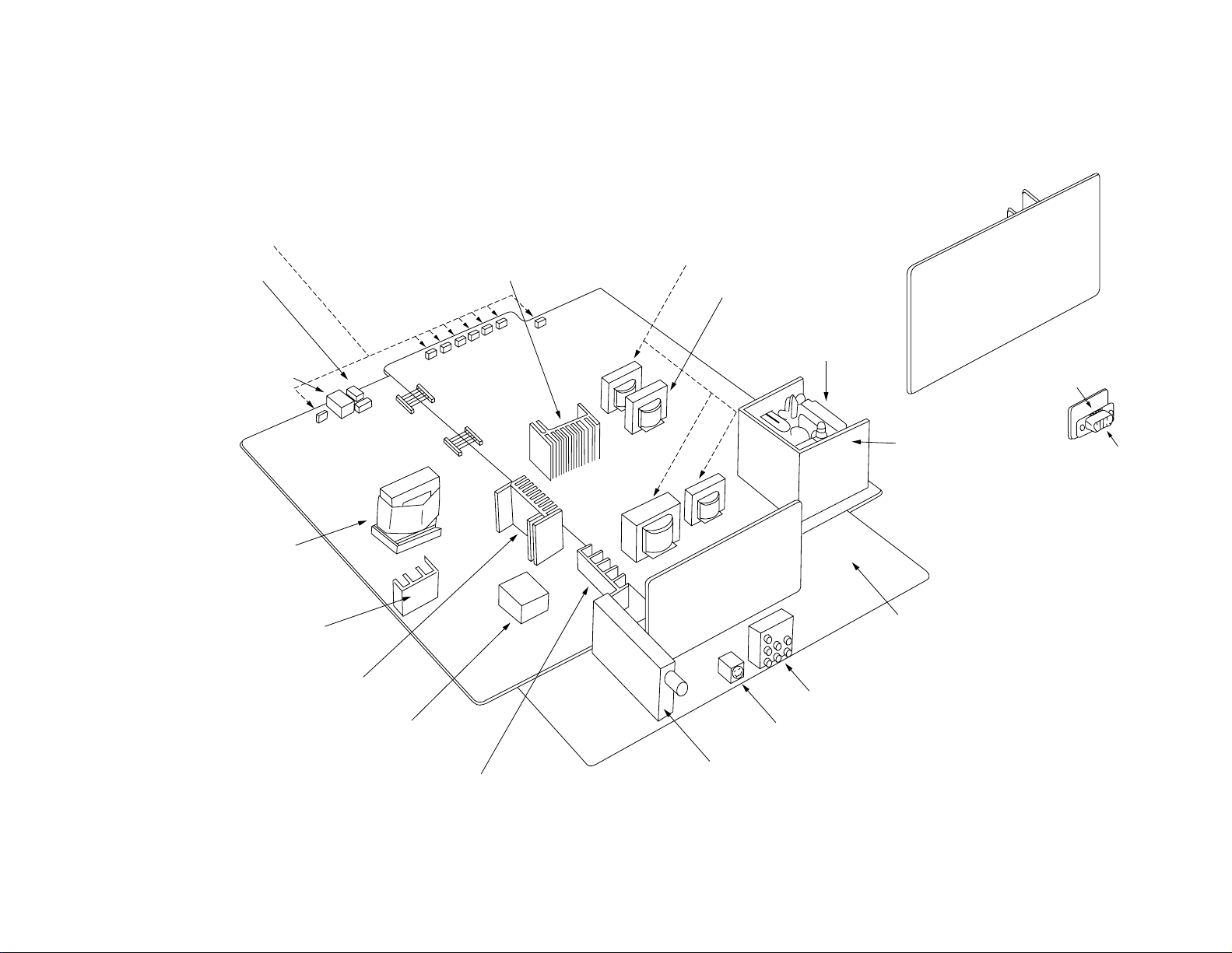
3. CONSTRUCTION OF CHASSIS
Choke coils
V out radiator
Choke trnas
Video unit
Flyback trans
D-sub unit
1-2
Power unit
Converter trans
Rectifier
Power radiator
Stand by trans
Sound out radiator
Def unit
V/C/D unit
Tuner
Jack board
S-VIDEO
H out radiator
Signal unit
D-sub connector
Page 5
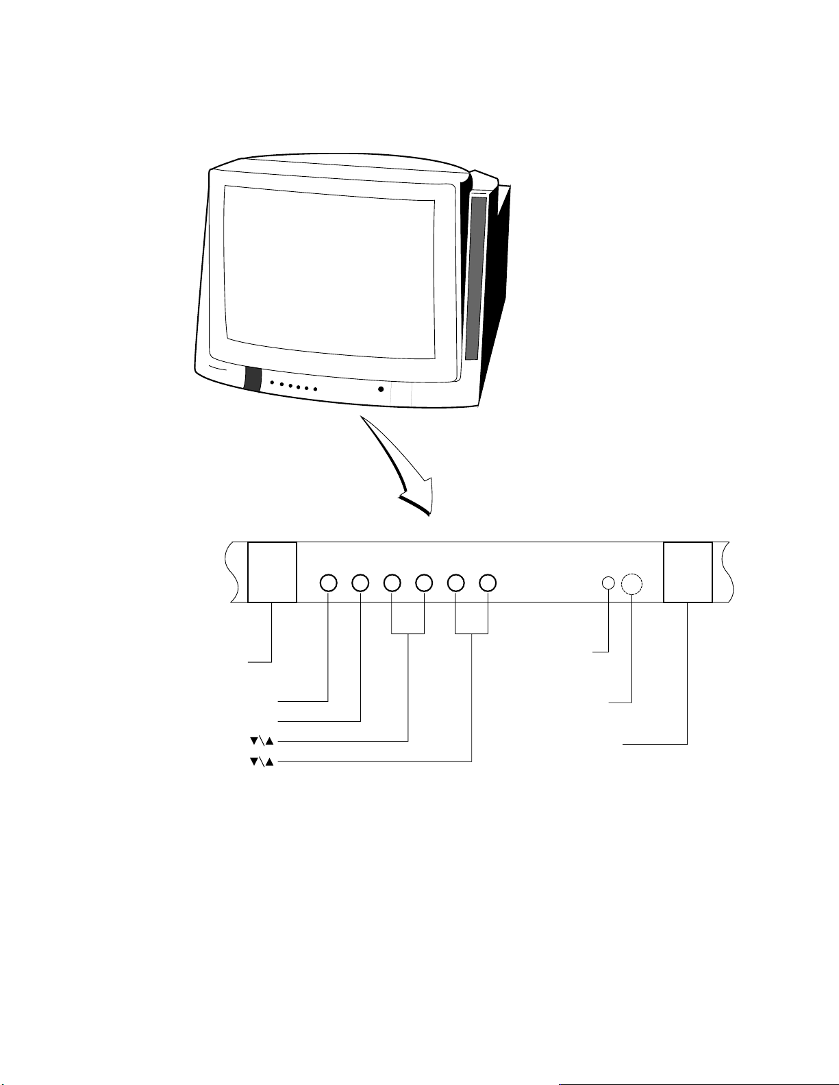
4. LOCATION OF CONTROLS
4-1 TV Set
RGB/
TV/VIDEO
button
MENU button
ADV button
VOLUME
CHANNEL
POWER indicator
REMOTE senser
POWER button
1-3
Page 6
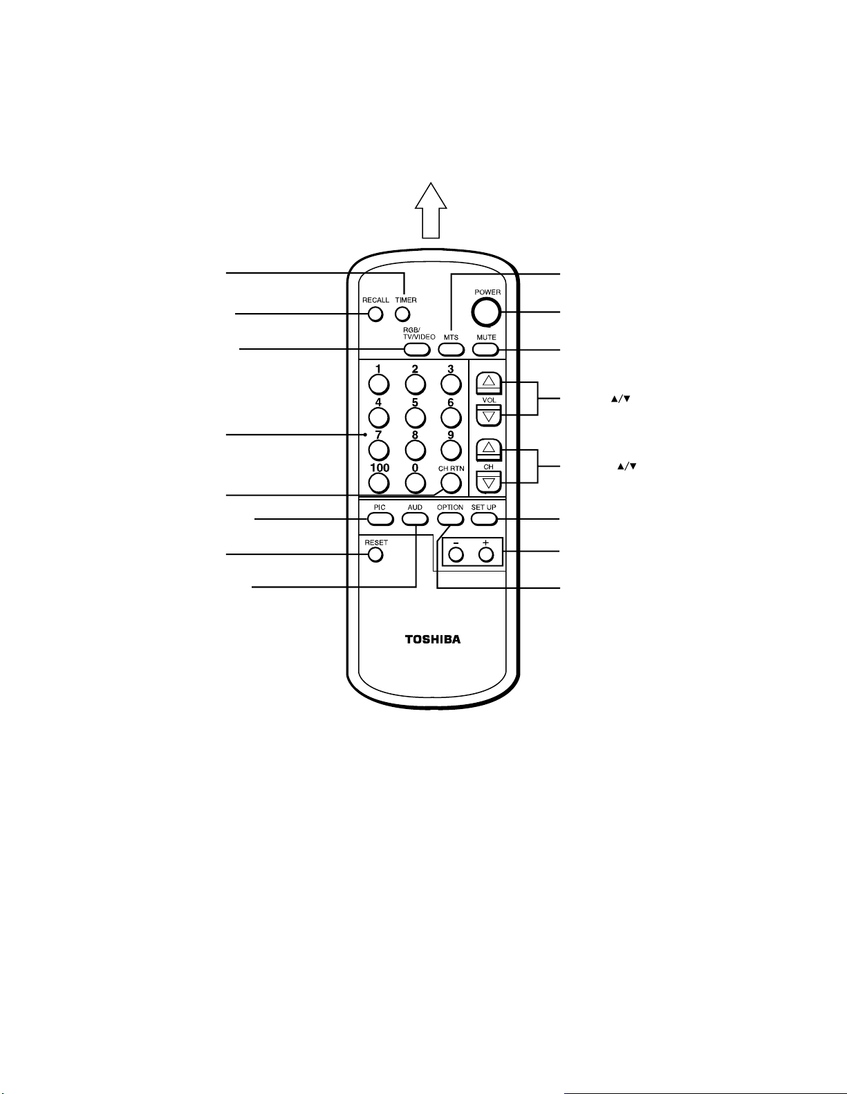
4-2 Remote Control
T
s
This Remote Control allows you to control the functions of your TV set from 16 feet (5m) away. The “*” marked function buttons
do not have duplicate locations on your TV set. They can be controlled only by the Remote Control.
Aim at the TV set
TIMER button*
RECALL button*
V/VIDEO button
Channel Number
buttons*
CH RTN (Channel Return)
button*
PIC (Picture)* button
RESET button*
AUD (Audio) button*
MTS button*
POWER button
MUTE button
VOLUME buttons
CHANNEL button
SET UP button*
-/+ buttons
OPTION button*
1-4
Page 7
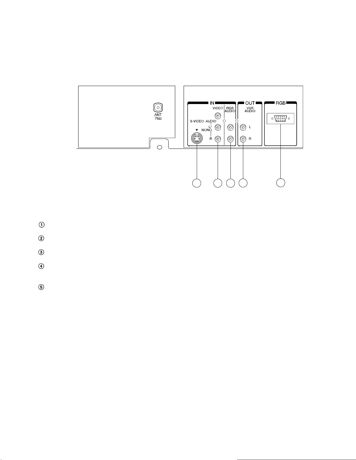
4-3 Monitor Panel
This TV set is equipped with RGB INPUT connector, RGB AUDIO INPUT jacks, S-VIDEO INPUT jack, VIDEO/AUDIO
INPUT jacks and VARIABLE AUDIO OUTPUT jacks of connecting your desired personal computer and video/audio
equipment.
TV Rear
3
4
5
2
1
RGB INPUT Connector – provide for direct connection of a personal computer.
RGB AUDIO INPUT Jacks – provide for direct connection of a personal computer with audio output terminals.
S-VIDEO INPUT Jack – provide for direct S-video connection from an S VHS VCR or a video disc player.
VIDEO/AUDIO INPUT Jacks – provide for direct connection of video devices (VCR, video disc player, camcorder, etc.)
with video/audio outputs.
VARIABLE AUDIO OUTPUT Jacks – feed volume-controlled stereo audio out from whatever displayed on the screen,
allows connection of audio amplifier and lets you adjust sound level with TV’s remote.
1-5
Page 8
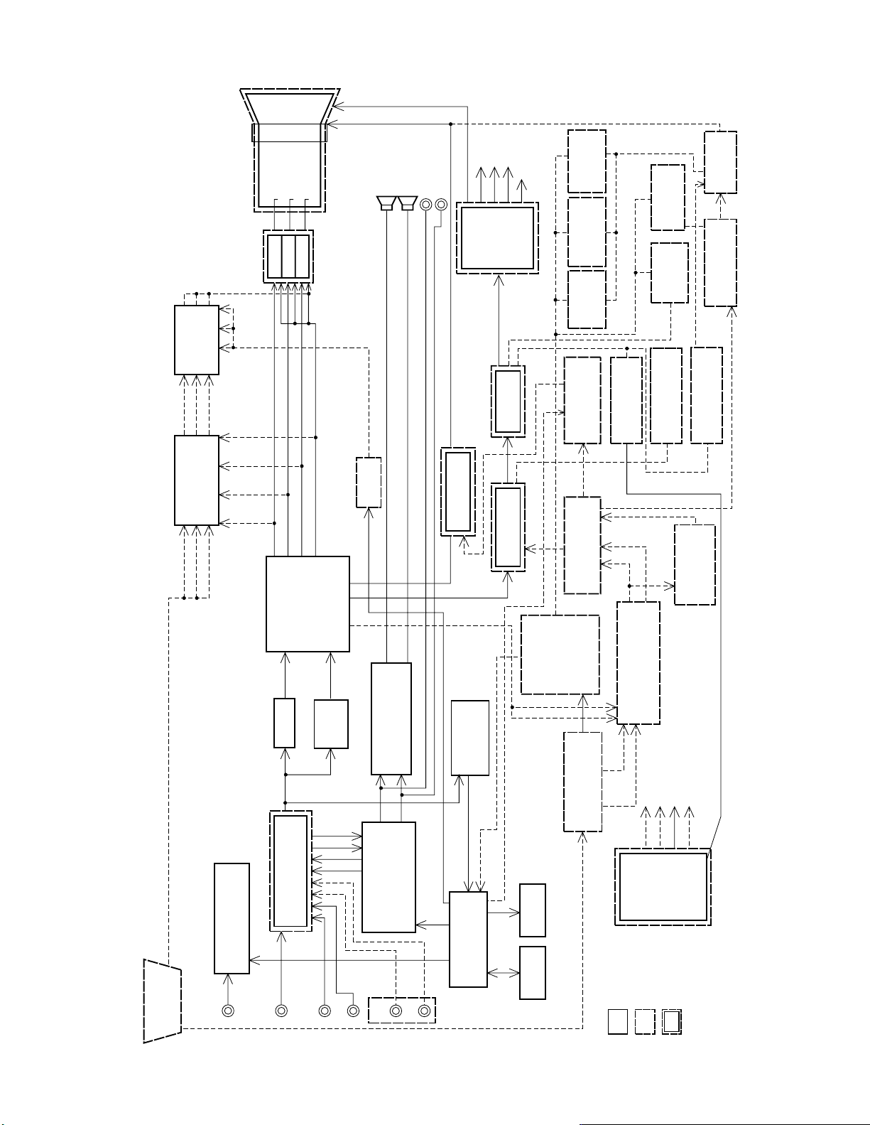
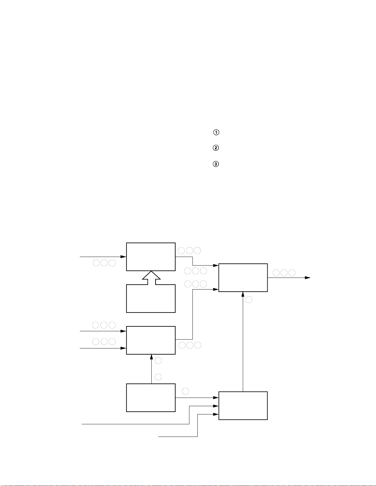
5. MM20E45 BLOCK DIAGRAM
EH
VAR. OUT
VIDEO
(VERT)
(+15V)
(HEATER)
capacitor
switching
Resonance
Drive
switching
output
Horizontal
Signal
switching
AN5862K
RGB
TA7730
Signal switching
RGB
FBT
G-output
B-output
R-output
output
Horizontal
OSD
LA7837
Vertical output
R-Y G-Y B-Y -Y
Horizontal drive
V/C/D
TA8801
Linear coil
switching
S-shape
capacitor
switching
DPC
TA8859AP
High voltage
control chopper
H
Horizontal/vertical
oscillation LA7860
V
capacitor
switching
Resonance
Drive
switching
F/V conversion
Horizontal drive
control chopper
Horizontal amplitude
IR9331
20VMMTV BLOCK DIAGRAM
D.L
TC4053BP
Signal switching
RGB
Tuner/IF module
RF
VIDEO
L
Band
pass
R
TA8200AH
Audio output
L
R
CXA1774S
Audio control
L
R
1-6
C. CAP slicer
Micro-computer
Mode distinction
TA75339AP
TC74HC86AP
TC4514P
TA75902
Synchronizing signal
process M52346SP
H.Sync
DAC
Memory
V.Sync
Syncon G
TC40538P
Synchronizing
signal switching
+15V
HEATER
Power unit
To be added
for MM
TV & MM
AUDIO
VERT.
+100V
Model change
( ) For MM
Page 9
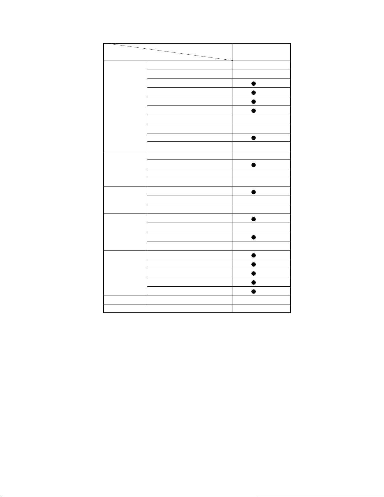
6. SPECIFICATIONS
SPECIFICATIONS
GENERAL
10 Local Keys 8key
11 Front Surround –
SOUND
PICTURE
OTHER
TERM
CABINET
12 Sub Bass System
13 Audio Output 5W x 2
14 Speaker Size & Nbr 80 x 120 x 2
15 Comb Filter (GLS)
16 Black Level Expand –
17 Horizontal Resolution 500
18 Parental-Ch Lock
19 Channel Caption –
20 Off Timer (180min)
21 Channel Search –
22 S-Video In-Term (1)
23 Audio, Video In-Term (1)
24 Variable Audio Out (RCA Jack)
25 RGB Audio (L, R)
26 Mini D-Sub 15pin
27 Rod-Ant/Adapter –/–
MODEL No.
1 Picture Tube D/T Invar
2 Channel Capacity 181ch
3 C. Caption
4 MTS with dbx
5 Bass, Treble, Balance
6 Sub Audio Program
7 Remote hand unit Regu.
8 Nbr of RMT Button 29key
9 LED Indicators (P)
MM20E45
NEW
1-7
Page 10
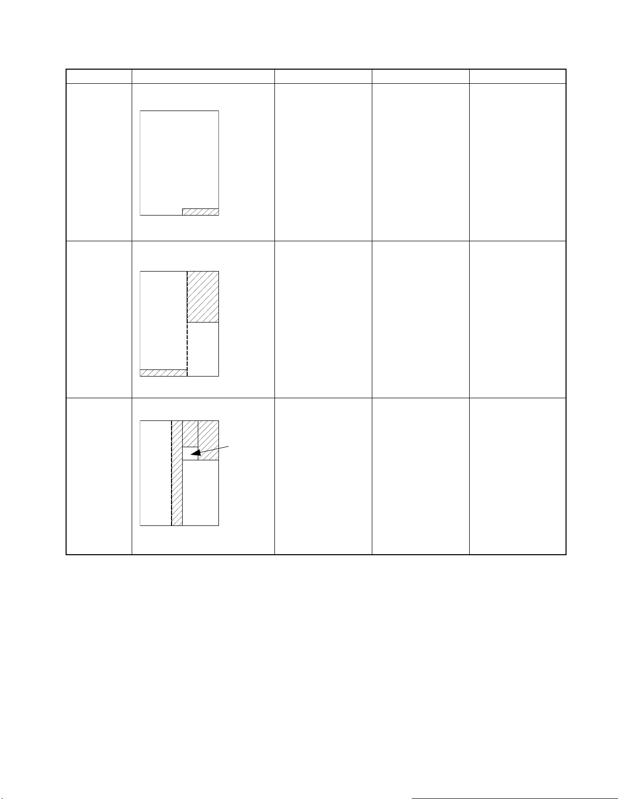
MM20E45 PC BOARD CONSTRUCTION
p
ITEM MM20E45 NEW MODEL CIRCUIT NOTE
DEF
PB5227
POWER/VCD
PB5226
249 x 330
249 x 330
POWER
dro
V/C/D
V-CUT LINE
Hole drawing: New
drop
Hole drawing: New
Hole drawing: New
Hole drawing: New
Def.
PB5227
(249.0 x 330.0)
Power/Audio
PB5226-1
(153.0 x 317.0)
Video/Chroma/Def
PB5226-2
(96.0 x 160.0)
Printed wiring board
part code
P/P-M/P:
23534680B
Printed wiring board
part code
P/P-M/P:
23534679B
SIGNAL/
VIDEO
PB5228
249 x 330
SIGNAL
VIDEO
-
drop
D-SUB
Hole drawing: New
Hole drawing: New
Signal
PB5228-1
(110.0 x 330.0)
Video (CRT/D)
PB5228-2
(119.0 x 210.0)
D-Sub
PB5228-3
(28.5 x 41.5)
Printed wiring board
part code
P/P: 23534681B
M/P: 23534681C
1-8
Page 11

SECTION II CHANNEL SELECTION CIRCUIT
1. OUTLINE OF CHANNEL SELECTION
SYSTEM
The channel selection circuit in the N5MM1 chassis employs
a bus system which performs a central control by connecting
a channel selection microcomputer to a control IC in each
circuit block through control lines called a bus.
In the bus system which controls each IC, the I2C-bus system
(two line bus system) promoted by Philips Co., Ltd. in the
Netherlands has been employed.
The ICs controlled by the I2C-bus control system are: ICG01
for audio system process, ICA02 for non-volatile memory,
H001 for main U/V tuners, IC302 for deflection distortion
corrections.
2. OPERATION OF THE CHANNEL
SELECTION CIRCUIT
2-1 Channel Selection Control Microcomputer
(ICA01 Toshiba TMP87CM34N-3101)
8 bit microcomputer, TLCS-870 series for TV receivers,
TMP87CM34N (42 pins, built-in CCD) developed by Toshiba
is employed. With this microcomputer each IC and circuit
shown below are controlled.
2-1-1 Non-volatile Memory IC
(ICA02 NEC µPD672CX)
(1) Memorizes data for video and audio signal adjustment
values, sound volume, woofer adjustment value, external
input status, etc.
(2) Memorizes adjustment data for white balance (RGB cut
off, GB drive), sub-brightness, sub color, sub-tint, etc.
(3) Memorizes deflection distortion correction value data
adjusted for each unit.
2-1-2 U/V Tuner Unit
(H001 Toshiba EL911L)
(1) A desired station can be received by transferring a
channel selection frequency data (division data) to the
I2C-bus type frequency synthesizer provided in the
tuner and by setting a band switch data which selects the
UHF or VHF band.
2-1-3 Deflection Distortion Correction IC
(IC302 Toshiba TA8859AP)
(1) Sets adjustment memory values for vertical amplitude,
linearity, horizontal amplitude, parabola, corner, pedestal
distortion, etc.
2-1-4 Audio System Process IC
(ICG01, SONY CXA1784S)
2-1
Page 12
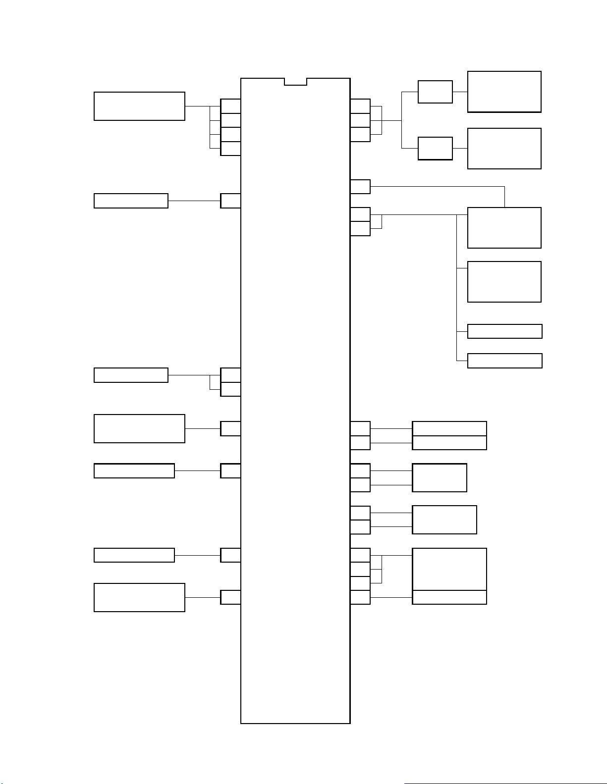
3. SYSTEM BLOCK DIAGRAM
VIDEO SIGNAL
PROCESS CIRCUIT
A/V DSP UNIT
25
24
23
22
10
QA01
TMP87CM34N-3101
Y
B
G
R
EXIT A
STB
CLK
DATA
AFT
SCL
SDA
37
38
DAC1
5
6
7
DAC2
9
PICTURE
CONTROL
AUDIO
CONTROL
TUNER/IF
MEMORY
µPD6272CX
QA02
KEY SWITCH
RGB MODE
DISCRIMINATION
RELAY DRIVE
SYNC SEPA.
REMOTE
CONTROLLER LIGHT
ERCEPTION UNIT
13
KEY A
14
KEY B
15 MODE
1
RELAY
35
SYNC
RMT
36
HD
VD
OSC1
OSC0
X1
X0
RST
HOLD
VDD
VSS
26
28
31
33
27
29
32
34
42
21
DPG
MTS
H. PULSE
V. PULSE
6.13 MHz
TRF1147T
8MHz CLOCK
TCR1056
RESET
CIRCUIT,
5V
GND
2-2
Page 13

3-1 Microcomputer Terminal Name and Operation Logic
Terminal No. Terminal name I/O control resistor
1 RELAY Positive logic
2 P.B
3
4 MUTE Positive logic
5 STB T BUS PERIOD
6 CLK T BUS CLOCK
7 DATA T BUS DATA
8 I-CSTOP Negative logic
9 AFT
10 EXTA TV: H VIDEO/RGB: L
11 SPKOFF Negative logic
12 LINE21
13 KEY1 Local key input 0~5V
14 KEY2 Local key input 0~5V
15 MODE RGB MODE input 0~5V
16
17 Y IN
18 B IN
19 G IN
20 R IN
21 VSS GND
22 R
23 G
24 B
25 Y
26 HD H sync pulse input
27 VD V sync pulse input
28 OSC1
29 OSC0
30 TEST For microcomputer shipping test. Fixed low level
31 X IN
32 X OUT
33 RESET Negative logic
34 STOP Negative logic
35 RMT Remote controller signal det. Negative logic
36 SYNC Sync pulse signal input
37 SCL I2C BUS CLOCK
38 SDA I2C BUS DATA
39 TC1 GND
40 CSIN
41 VIN
42 VDD Microcomputer power supply
Oscillation connection terminal for OSD circuit
6.13MHz TRF1147T
High frequency oscillation connection terminal
Part for caption
2-3
Page 14
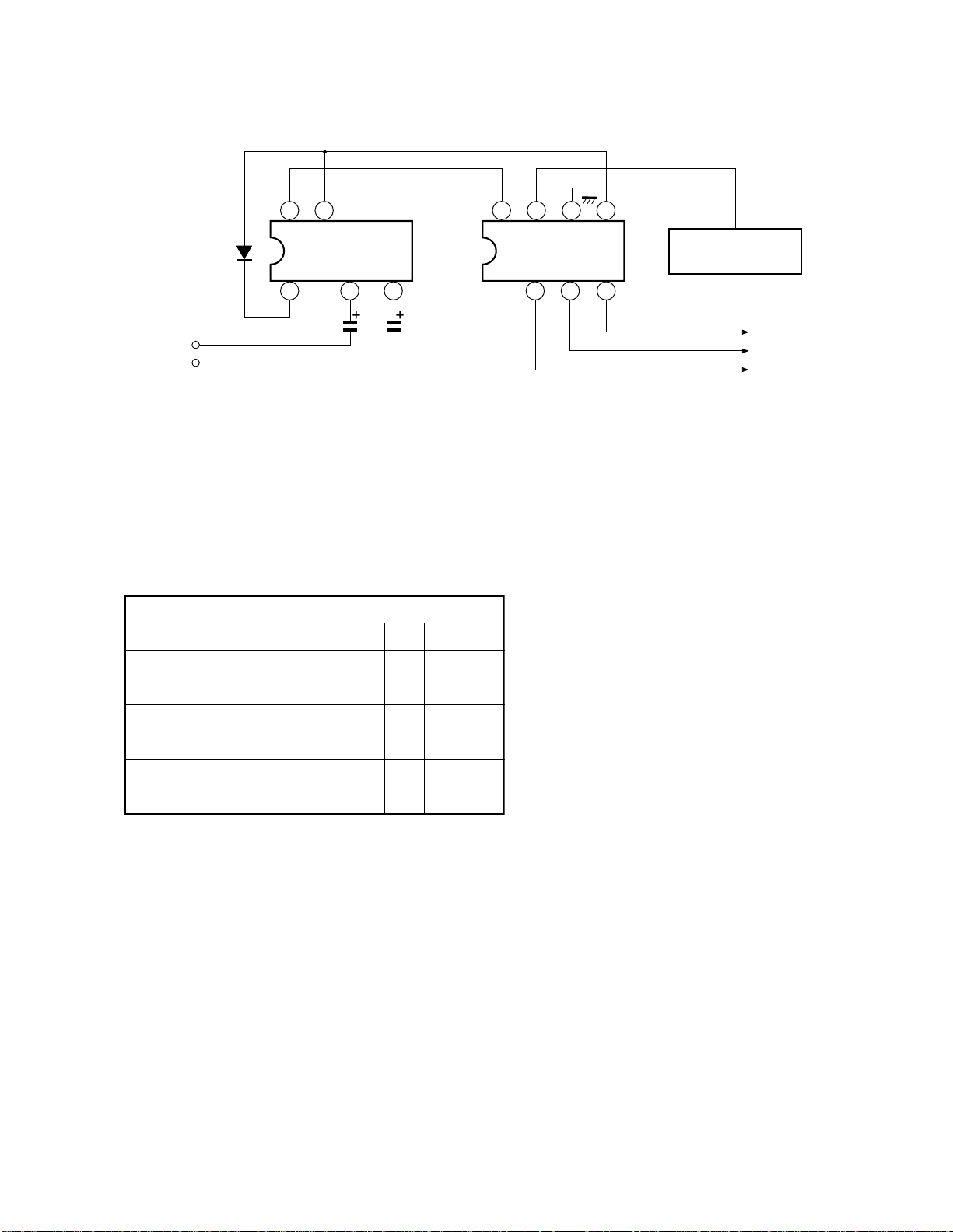
3-2 DAC Terminal Name and Operation Logic
(1) DAC (QX01)
Terminal No. Terminal name Function I/O Logic
1 VDD INTERFACE POWER SUPPLY
2 DAT T-BUS DATA INPUT TERMINAL I
3 CLK T-BUS CLOCK INPUT TERMINAL I
4 PRD T-BUS PERIOD INPUT TERMINAL I
5 RESET
6 SUB-ADDRESS CHANGEOVER TERMINAL O
7 RGB CONT RGB CONTRAST O 0~5V
8 VSS GND
9 SBS SUB BASS SYSTEM O ON: L OFF: H
(H at SPK OFF)
10 RGB BRT RGB BRIGHTNESS O 0~5V
11 TNT TINT O 0~5V
12 COLOR COLOR O 0~5V
13 SHARP SHARPNESS O 0~5V
14 BRT BRIGHTNESS O 0~5V
15 CONT CONTRAST O 0~5V
16 VCC POWER SUPPLY
(2) DAC (QX001)
Terminal No. Terminal name Function I/O Logic
1 VDD INTERFACE POWER SUPPLY
2 DAT T-BUS DATA INPUT TERMINAL I
3 CLK T-BUS CLOCK INPUT TERMINAL I
4 PRD T-BUS PERIOD INPUT TERMINAL I
5 RESET
6 SUB-ADDRESS CHANGEOVER TERMINAL O
7 TV/RGB TV/RGB SWITCH TERMINAL O TV: L RGB: H
(L at RGB NO SIG.)
8
9 MUTE VIDEO MUTE O NEGATIVE LOGIC
10 H-POS H-POSITION O 0~5V
11 H-SIZ H-SIZE O 0~5V
12 V-POS V-POSITION O 0~5V
13 TV/RGB TV/RGB SWITCH TERMINAL O TV: H RGB: L
14 NO SIG NON/YES SIGNAL OUTPUT O YES: H NON: L
15 SUB CONT SUB CONTRAST (TV) O 0~5V
16 VCC POWER SUPPLY
2-4
Page 15
3-3 Remote Control Code Assignment
Custom codes are 40H.
Key
No.
Data
code
Function
K1 00H 0
K2 01H 1
K3 02H 2
K4 03H 3
K5 04H 4
K6 05H 5
K7 06H 6
K8 07H 7
K9 08H 8
K10 09H 9
K11 0AH 100
K12 0BH
K13 0CH RESET
K14 0DH AUDIO
K15 0EH PIC
K16 0FH RGB/TV/VIDEO
K17 10H MUTE
K18 11H
K19 12H POWER
K20 13H MTS
K21 14H OPTION
K22 15H TIMER
K23 16H SET UP
K24 17H CH RTN
K25 18H
K26 19H CONTROL UP
K27 1AH VOL UP
K28 1BH CH UP
K29 1CH RECALL
K30 1DH CONTROL DN
K31 1EH VOL DN
K32 1FH CH DN
K33 40H
K34 41H
K35 42H
K36 43H
K37 44H
K38 45H
K39 46H
K40 47H
K41 48H
K42 49H
K43 4AH
K44 4BH
K45 4CH
K46 4DH
K47 4EH
K48 4FH
Continuity
Key
No.
Data
code
K49 50H
K50 51H
K51 52H
K52 53H
K53 54H
K54 55H
K55 56H
K56 57H
K57 58H EXIT
K58 59H
K59 5AH SET UP
K60 5BH OPTION
K61 5CH
K62 5DH
K63 5EH
K64 5FH
K88 97H
K109 CCH
K110 CDH
K111 CEH
K112 CFH
Function
Continuity
2-5
Page 16
3-4 Local Key Assignment
1. Detection method of Local Key
Detection method of Local Key in N4ES chassis is analogue way to detect what voltage appears at local key input terminals
(pins 13, 14) of Micom when the key is pressed.
By this method, key detections of a maximum of 7 keys can be done, using local key input terminal (pin 13). As seen in the Local
key circuit below, when one of key among S13-1 to S13-7 is pressed, the VIN which corresponds to the switch is applied to input
terminal (pin 13). Judgement of key-input is done by measuring what voltage VIN is at the pin. Voltage measuring and key
judgement are performed by A/D converter in Micom and by the software.
KEY No. Function
S13-1 POWER
S13-2 CH UP
S13-3 CH DN
S13-4 VOL UP
S13-5 VOL DN
S13-6 ADV
S13-7 MENU
S14-1 RGB/TV/VIDEO
LOCAL KEY Assignment table
33K
7.5K
7.5K
11K
16K
30K
68K
KEY1
33K
13 14
S13-1 S14-1
S13-2
S13-3
S13-4
S13-5
S13-6
S13-7
KEY2
2-6
Page 17
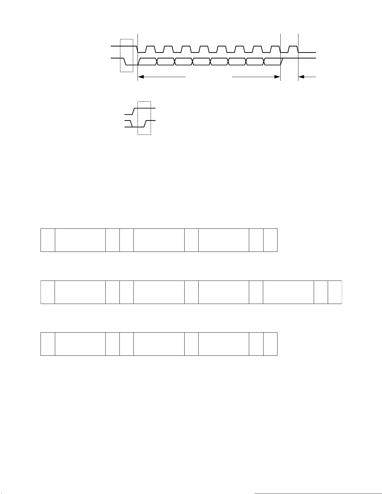
4. I2C BUS INTERFACE OPERATION TIMING
p
As an example of I2C Bus interface operation timings,
control for a memory IC will be shown below.
4-1 Write Mode (1 Byte)
DA
CL
Start bit issue
4-2 Read Mode
SDA
SCL
Start bit issue
1
0
15243
Slave address
R/W command input
Slave address
1
1
0
1
0
Slave address
R/W command input
R/W
2
1
A
0
A
6789
1
ACK signal
output
R/W
A
A
2
1
00
5243
789
6
ACK signal
output
ACK(OUT)
WA7WA6WA5WA4WA3WA2WA1WA
00
Word address
input
ACK(OUT)
WA7WA6WA5WA4WA3WA2WA1WA
Word address
input
Fig. 2-1
0
ININ
Start bit issue
ACK signal
input
ACK(OUT)
D7D6D5D4D3D2D1D
0
ACK signal
output
Word address
update
Stop bit issue
After completion of write operation
word address becomes the write
address +1 and held at that value.
R/W
ACK(OUT)
2
1
A
0
A
6789
1
1
00
15243
IN
Slave address
R/W command input
ACK signal
out
ut
0
INININ
Write data
input
D7D6D5D4D3D2D1D
ACK signal
output
OUT
Read data
output
ACK signal
input
ACK(OUT)
ACK(IN)
0
IN
Stop bit issue
Fig. 2-1
2-7
Page 18
4-2-1 Generation of Start/stop Status
SCL terminal
DA termianl
SCL terminal
SDA termianl
4-3 I2C Bus Data Format
(1) Memory IC
* Write mode
Start
condition
152637489
D7 D6 D5 D4 D3 D2 D1 D0
Data transmission
Acknowledge
signal
Stop
condition
Fig. 2-3
S
Slave address
8 bits
A0H (WRITE)
* Read mode
S
Slave address
8 bits
(2) DPC IC
S
Slave address
8 bits
8CH
RW AC
AC
RW
RW AC
Word address
8 bits
Word address
8 bits
Sub-address
8 bits
AC
AC
AC
Data 8 bits
Slave address
8 bits
Data 8 bits
AC ST
AC
AC ST
Data 8 bits
AC ST
2-8
Page 19

(3) U/V tuner unit
S
Slave address
8 bits
RW AC AC ST
FM
8 bits
AC
Main screen tuner: COH
FM: Variable divider control byte
FL: Variable divider control byte
CO: Charge pump sensitivity switching bit and test mode bit
BA: Band switching bit
FL
8 bits
AC AC
CO
8 bits
BA
8 bits
2-9
Page 20
5. SERVICE ADJUSTMENT MODE
1. Entering to Service Adjustment mode
Press MUTE key on the remote control unit once.
Press again the MUTE key, and keep pressing it.
Keep pressing the MUTE key, press MUTE key on TV set.
120H 8DH
Adjusting picture of NTSC mode
2. Switch-over of Service Adjustment mode
Every pressing of MENU key makes main address switch
over.
161H 1E2H 120H 114H
Address
161H Video section sub-adjustment
1E2H OSD horizontal starting position
120H Deflection section sub-adjustment
Adjustment contents
120H 8DH
RGB 350
Adjusting picture of RGB mode
4. Adjusting method of data
Pressing ADJUST UP/DOWN key on remote control
unit changes the data value ranging from 00H to FFH.
5. Cancellation method of Service mode
The operation of key that accompanies display of
other than from 1 to 4 makes the mode cancel.
During servicing in RGB mode, changing of the
mode of RGB causes cancellation.
Address, Data
Mode display of RGB
114H Multi-sound adjustment
3. Switch-over within Service Adjustment mode
Pressing of VOL UP key on remote control unit or on TV
set makes address switch over cyclically, and VOL DN
key switches over in reverse direction.
a) 161H 107H 163H 108H
b) 1E2H
c) 120H 121H 122H 123H 125H 126H
127H 128H 12AH 111H 112H
d) 114H 115H 116H 116H 117H 118H
119H
6. Other service function
MUTE key : Shipping-out preset
RECALL key: Initializing of memory
2-10
Page 21
ADDRESS OF SERVICE MODE
a) Video section sub-adjustment
Address
161H SUB BRIGHT
107H SUB COLOR
163H SUB TINT
108H SUB CONTRAST
c) Deflection section sub-adjustment
Address
120H PICTURE HEIGHT
121H V-LINEARITY
122H V-S CORRECTION
123H V-SHIFT
125H PICTURE WIDTH
126H E-W PARABOLA
127H E-W CORNER
Adjustment contents
Adjustment contents
b) OSD horizontal starting position
Address
1E2H OSD-H.POSI
d) Multi-sound adjustment
Address
114H ATT
115H STEREO VCO
116H SAPVCO (MSB)
116H SAPLPF (LSB)
117H FILTER
118H SPECTRAL
119H WIDEBAND
Adjustment contents
Adjustment contents
128H KEYSTONE
12AH V-CORRECTION
111H HORIZ POSITION
112H VERT POSITION
2-11
Page 22
SECTION III RGB SIGNAL PROCESSING CIRCUIT
1. OUTLINE
The signal flow is explained as follows. RGB signal is input
to D-SUB 15P and is processed to be output at CRT Drive
circuit.
2. OPERATION AND FLOW OF RGB
SIGNAL
Fig. 1 shows flow chart of RGB signal.
3. CIRCUIT OPERATION
(1) RGB signal input at D-SUB 15P is supplied to pins 2, 6,
10 of RGB signal processing IC M52327SP respectively.
(2) The signal which is input to RGB signal processing IC,
is processed in four steps ; 1) Amplification, 2) Contrast
control, 3) Brightness control, 4) Black level clamp.
After that, the signal is output at pins 28, 24, 20 and then
is input to pins 1, 2, 3 of Signal switching IC AN5862K.
(3) In TV reception, R-Y, G-Y and B-Y outputs of IC501
TA8801AN are selected by IC216 AN5862K and ICR03
AN5862K, and are output at pins 5, 6, 8 of ICR03
AN5862K.
(4) TV/RGB switching pulse output from ICX001
TB1203AP, OSD switching pulse output from
microcomputer and blanking pulse are input to OR gate
circuit. And output from OR gate is input to pin 4 of
ICR03 AN5862K.
These operations function as following 3 items.
In TV mode, output from ICR03 AN5862K is
turned over to TV.
In RGB mode, OSD signal is made by OSD
switching pulse from OR gate.
In RGB mode, blanking is performed.
A8801AN
R-Y, G-Y, B-Y
utput
MICOM
OSD output
MICOM
Y output
(1)
RGB input
62
10
13 12 11
(3)
ICR02
RGB AMP
M52327SP
1) SIGNAL AMP
2) CONTRAST
3) BRIGHTNESS
4) CLAMP
321
IC216
SIGNAL
SWITCHING
AN5862K
4
3
ICX001
SWITCHING
SIGNAL
GENERATOR
TB1203AP
28 24 20
13 12 11
7
(2)
865
321
ICR03
SIGNAL
SWITCHING
AN5862K
4
(4)
OR
GATE
865
Signal
output
Blanking pulse
Fig. 1
3-1
Page 23
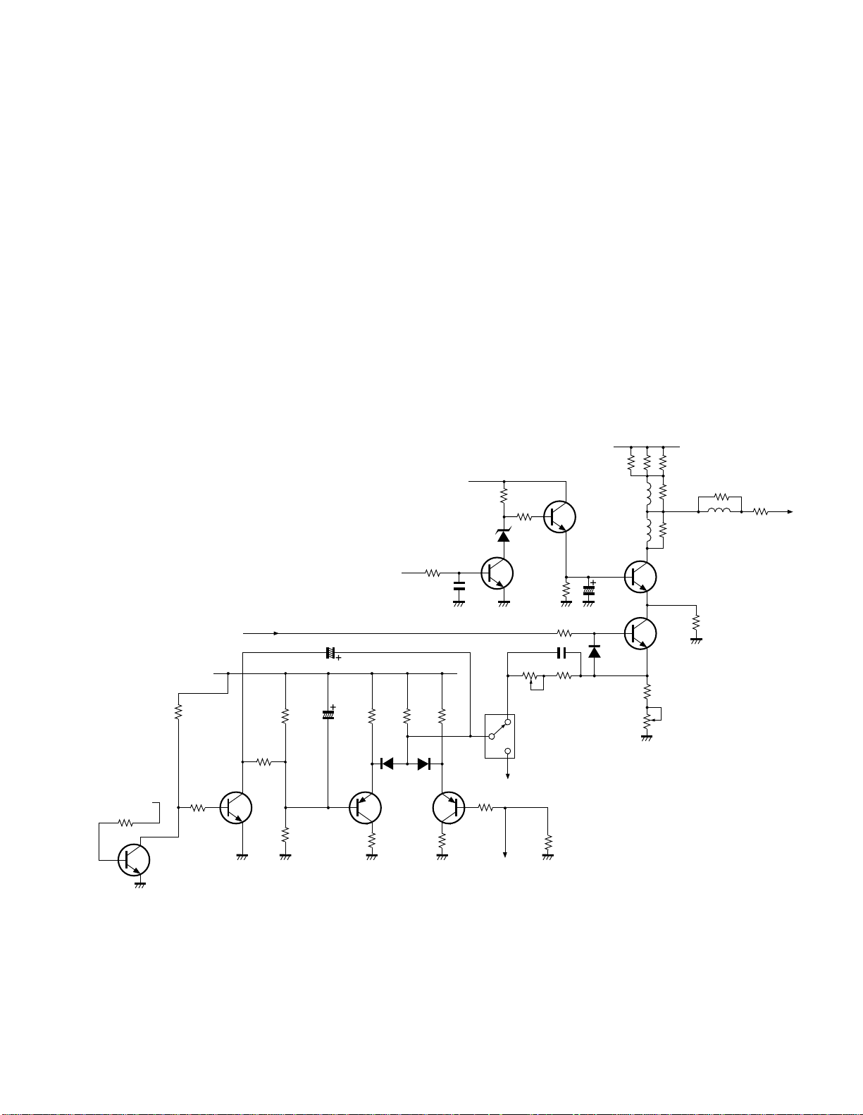
SECTION IV CRT DRIVE CIRCUIT
1. OUTLINE
CRT Drive circuit is designed with its output load resistance
decreased, to obtain wide frequency band, and heat-sink of
output transistor is enlarged in size. Cut-off control and
Drive control of TV signal are adjusted with variable resistors
on CRT drive circuit, otherwise RGB signals are adjusted by
bias control and gain control of RGB AMP ICR03 M52327SP.
2. CIRCUIT OPERATION
For example, Green axis circuit is explained as follows.
(1) G signal which is output at pin 6 of AN5862K, is
supplied to the base of Q904, and is amplified in wide
band by Q903 and Q904. Then it is input to cathode of
CRT.
(2) The level of pin 7 of ICX001 TA1203AP becomes (L)
in RGB and (H) in TV. Utilizing this level change,
emitter bias level of Q904 is changed over RGB mode
and TV mode.
(3) The MUTE signal is generated at pin 9 of ICX001 in
POWER ON/OFF, CH selecting, MODE changing.
This signal turns Q903 to cut-off to prevent disorder of
picture from displayed on screen.
(4) Cut-off and Drive controls can be adjusted with R952
and R954.
+200V
+12V
RR25
DR08
RR26
L905
QR05
L904
R922, R923, R924
R925
R921
L906
R920
R926
KG
ICX001 TA1203AP
TV/RGB
Pin7
R209
Q206
+12V
R207
R941
ICR03
Pin6
R943
R942
Q907
ICX001 TA1203AP
MUTE Pin9
C909
C910
R944
R946
R964
R945
D904
Q908
RR24
CR13
R947
D905
Q904
Fig. 1
R961
DEF Circuit
R948
-Y
QR04
R927
R954
SERVICE
SWITCH
R914
C904
R918
R949
Q903
C907
R915
Q904
D902
R918
R952
4-1
Page 24
SECTION VMODE DISCRIMINATION CIRCUIT AND SYNC
SIGNAL PROCESSING CIRCUIT
Mode discriminating circuit performs to discriminate the kind of signals ; the signal which is input to D-SUB connector, is VGA,
or is Macintosh signal.
Sync signal processing circuit performs to process sync signals into shape which can be utilized in horizontal and vertical osc
circuits, because the signals which are input to D-SUB connector from a personal computer have various figures.
1.OUTLINE OF MODE DISCRIMINATING CIRCUIT
This model, for the simplification, reduces discriminating functions than CRT monitor for computer. The functions are those:
to identify VGA signal or not; horizontal scanning frequency is higher or lower than 28kHz; the signal is input or not.
NO SIGNAL
DISCRIMINATION
ICH01, QH06
No signal
Hor. sync
Vert. sync
POLARITY
DISCRIMINATION
ICH01
FREQUENCY
DISCRIMINATION
ICH04, ICH05
DECODER
ICH02
VGA480
VGA400
VGA350
Low frequency
Fig. 1
VGA has three modes by number of vertical line. These are made to be able identify by polarity of horizontal and vertical sync
signal. The difference of VGA mode signal is described in Table-1.
Kind No. of Ver. line fH fV Hor. Sync polarity Ver. Sync polarity
VGA480 480 31.5kHz 60Hz Negative Negative
VGA400 400 31.5kHz 70Hz Negative Positive
VGA350 350 31.5kHz 70Hz Positive Negative
Table-1
The above discriminated output is supplied to Ch. selection IC ICA01, and to be used as a sign to switch operations of related
circuit.
5-1
Page 25
2. OUTLINE OF SYNC SIGNAL PROCESSING CIRCUIT
As mentioned above, signal input at D-SUB connector from personal computer, sometimes shows various shape of sync signal.
Representative signals are described in Table-2.
Kind Resolution fH Fv Hor. Sync polarity Ver. Sync polarity
IBM PGC 640 x 480 30.5kHz 60Hz Composite Sync
IBM VGA480 640 x 480 31.5kHz 60Hz Negative Negative
IBM VGA400 640 x 400 31.5kHz 70Hz Negative Positive
IBM VGA350 640 x 350 31.5kHz 70Hz Positive Negative
SVGA 800 x 600 35.2kHz 56Hz Positive Positive
Macintosh 13Ó 640 x 480 35.0kHz 67Hz Sync on Green or Composite Sync
VESA VGA 640 x 480 37.9kHz 72Hz Negative Negative
Table-2
Roughly classified, they are of two shapes; one is, like Macintosh, SYNC ON GREEN which is imposed on video signal, and
the other is the output in TTL level separated from video signal. The TTL level method is classified to Composite Sync which
combines horizontal and vertical sync, and to Separate Sync which separates respectively.
And besides, in Separate Sync method, polarity is different by kind of signal.
Even though these various sync signal are input, always positive polarity of hor and ver sync signal is supplied to horizontal
and vertical sync osc circuit. This is the role of this circuit.
5-2
Page 26
3. MODE DISCRIMINATING CIRCUIT OPERATION
h
The circuit which discriminates three modes of VGA, is as follows.
DH31
19 18
ICH01
M52346SP
13 12 11 10
BCDA
ICH02
TC4028BP
fH > 28KHz/Hig
FREQUENCY
DISCRIMINATION
2
Hor. sync
Vert. sync
6 8 4 6 7
VGA350
VGA400
VGA480
Fig. 2
Mode discrimination of VGA is done by the circuit in Fig. 2. ICH01 M52346SP also performs process of sync signal, and the
logic output is shown in Table-3. ICH02 is Decoder IC TC4028BP, and the truth table is shown in Table-4.
Input at pin 6
H. COMP.
H. COMP. (POS.)
H. COMP. (POS.)
H. COMP. (POS.)
H. COMP. (NEG.)
H. COMP. (NEG.)
H. COMP. (NEG.)
NON
NON
NON
Input at pin 8
V.
NON
V. (POS.)
V. (NEG.)
NON
V. (POS.)
V. (NEG.)
NON
V. (POS.)
V. (NEG.)
Output pin
1 2 18 19
H
L
L
H
H
H
H
H
H
L
L
L
L
H
L
L
H
H
H
H
H
L
L
H
L
H
L
L
L
H
L
L
H
L
L
H
Table-3. Logic output of M52346SP Table-4. Truth table of TC4028BP
When Macintosh signal is input in form of negative composite sync, diode DH31 prevents confusion between Macintosh signal
and VGA400.
5-3
Page 27
The outputs of VGA three modes are tabled as in Table-5.
ICH01 M52346SP ICH02 TC4028BP
Kind
pin 6 pin 8 pin 18 pin 19
pin 11
(D)
pin 12
(C)
pin 13
(B)
pin 10
(A)
output
(High)
VGA480 Nega Nega H H L H H H pin 4
VGA400 Nega Posi H L L H L H pin 6
VGA350 Posi Nega L H L H H L pin 7
Table-5
As shown in table above, since the result of frequency discrimination is input to pin 12 (c) of decoder ICH02, in case that
frequency of input signal is lower than 28kHz, the mode is discriminated as not VGA mode even though polarity of sync signal
is same combination as VGA.
Operation of frequency discriminating circuit is explained as follows, and configuration is shown in Fig. 3.
+12V
RH90
27K
RH64
33K
RH48
22K
CK24
M0.015
Hori. Sync
RH09
QH03
2SC752Y
DH03
1SS176
or
1SS133
12K
CH12
SL100P
RH10
QK11
2SC1815Y
or 2SC17405,Q
or 2SC1685Q
18K
CH14
M2.2
RH12
10K
RH13
10K
RH11
15K
RH14
10K
7
8
ICH04
IR9331
F/V CONVERTER
2
1
RH16
RH18
1/4W4.7KF
1/4W
82KF
3
2
1
F/V ADJ
H. OSC
Def. circuit
6
3
RH17
2KB
5
4
RH15
5.6K
CH13
T1200
CH15
16V47
2
RH19
68K
RH21
1/4W11KF
RH75
8.2K
RH24
1/4W3.3KF
1
RH52
10K
3
RH26
1/4W1.8KF
RH20
1/4W
47KF
13
14
2
1
RH28 580K
+5V
DH04
1SS176
or
1SS133
RH23
1.8KG
11
12
ICH05
TA75902P
or LM2902N
3
4
RH27 680
QH10
2SC1815Y
or 0
DH06
RD5.1ESAB1
or UZ5,1BSA
RH22
560KG
RK59
10
5
RK58
33KG
12KG
98
6
RH29
1/4W
13KF
RH30
1/4W
8.2KF
DK17
1SS176
1SS133
7
H.Size
or
CK17
M680
F/V
LOW FREQ
QH09
RN1202
Fig. 3
ICH04, F/V (Frequency-Voltage) converter, produces the voltage proportional to hor. scan frequency of input signal.
This voltage is amplified in ope. amp ICH05. The comparator which is consisted of ICH05, compares frequency to operate
so that emitter voltage of OH10 becomes HIGH level when the frequency is high.
5-4
Page 28

Block diagram of ICH04 IR9331 is shown in Fig. 4.
t
Vcc
8
Current Output
Reference Voltage
Frequency Output
Current
1
2
Output Circuit
3
SW
1.90V
15
Mirror
Circuit
11
Reference
1.90V
Voltage
Each
Bias
Circuit
4
GND
Fig. 4
Comparator
R-S
Flip Flop
Timer
Comparator
R
7
6
5
2R
Comparator Inpu
Threshold
R-C
Operation of F/V converter circuit using this IC are as
follows.
When horizontal sync signal is input to pin 6 of IC through
QH03, this performs as a trigger, charge of capacitor CH13
which is connected to pin 5 begins. Voltage at pin 5 is
compared with reference voltage(Vcc x 2/3) by the comparater
inside IC, and the voltage finally reaches the reference
voltage to reverse the comparater. This reverse operation
discharges the capacitor rapidly. Next, when hor sync signal
comes, this operation is again repeated.
The period that this capacitor is being charged is constant, in
spite of input signal.
Hor. Sync
pulse
Voltage
of pin6
Voltage
of pin5
Current
of pin1
0
2
Vcc
3
0
0
1.9V
RH16+RH17
5-5
Tc
TH
Fig. 5
Page 29

In this period, current is supplied to capacitor CH14. This
y
current is a constant current which is made in CURRENT
MIRROR circuit, and is set with resistor RH18 connected to
pin 2. The voltage (1.9V) at pin 2, which is divided by
resistance of RH18, produces the current. The current flows
through CH14. Therefore, average voltage at pin 1 is decided
by the formula below.
1.9V
E =
RH16+RH17
RH18
•
TC
1.9V
=
•
TH
RH16+RH17
• 82kW •TC • fH (V)
DH04, RH22 and RH23 perform to limit F/V convert voltage
so that it does not rise extremely, even though the higher
frequency than responsive range of this model, is input. The
circuit using Ope Amp from pin 8 to pin10 of ICH05 limits
F/V convert voltage so that it does not decreases below
specified value when input signal does not come.
The voltage at pin 1 which is limited by the upper and lower
values, is amplified through amplifier of from pins 12 to 14
of ICH05. The amplifying character is set to the suitable one
to control free-running frequency of hor osc circuit.
As understanding from the above formula, at pin 1, the
voltage which is proportional to frequency of hor sync
signal, is obtained.
QK11 performs the function to prevent picture bending on
screen by the increase of F/V convert voltage, because the
period of equalized pulse is seemed as twice of frequency
when composite sync including equalized pulse like NTSC
within hor sync. is input. Countermeasure to this trouble is
to eliminate trigger pulse only for ver sync period.
Operation of no signal det. circuit is as follows.
M52346SP
Output voltage of this amplifier is compared with the reference
voltage by the comparater of pins1 to 3. When hor frequency
is high, the voltage at pin 1 becomes HIGH level. The
reference voltage of this comparater is selected so that the
comparater turns reverse when frequency is approximately
28kHz. The output of the comparater turns reverse to
become mode discriminating output, and besides it is used to
switching of circuit operation at some points in the hor
deflection circuit.
+5V
14
ICH01
86421
No signal
QH07
Green Video
Hor. sync
Vert. s
nc
QH06
Fig. 6
ICH01 is used in this circuit, which is explained in Mode discriminating circuit of VGA. This IC contains inside the function
which discriminates existence of hor-ver sync signal at pins 6 and 8. When the sync signal as shown in Table-3 does not exist,
logic outputs at pins 1 and 2 turn LOW to level. But, in Sync On Green method, discrimination whether sync signal is existed
or not is impossible. Therefore discriminating circuit is added by connecting QH06 to pin 14 at which hor sync signal is input.
The added circuit performs that emiter voltage turns to LOW level only when hor sync signal does not exist.
No signal situation is detected by way that these three output is set up in OR logic by diodes, collector voltage of QH07 is turned
to HIGH level.
5-6
Page 30

4. SYNC SIGNAL PROCESSING CIRCUIT
This circuit also employs ICH01, the same as Mode discriminating circuit.
Posi Non
Posi Non
Posi Non
Posi Non
Posi
Posi
Non
Non
H.Pol.
Neg
Neg
V.Pol.
Neg
Neg
H.State
Neg
Neg
V.State
Neg
Neg
Clamp
Clamp
Timing
20 19 18 17 16 15 14 13 12 11
Logic
Logic
1
Green
Sep
Filter
Clamp
Gen.
Clamp
Out
Sync
Sep.
Green
IN
Green
Edge
SW
Vcc
5432
GND
12V
HD
Out
Comp/H
IN
Comp/H
Hor.
Shape
Comp/H
Out
Det
HD
Hor.
Det
H.Det
VD
Out
Vert
IN
Vert.
Shape
Vert
VDHDHD
Digital
GND
Vert
Det
Vert.
Det
+
Vert
S/S
IN
V.Sync
Sep.
9876
10
Vert
S/S
Adj
Digital Vcc
(5~12V)
GND
Sync signals are input as follows; TTL level hor sync or
composite sync to pin 6, TTL level ver sync to pin 8, and Sync
On Green sync to pin 4. Output signals are as follows;
Positive ver sync at pin 13, Positive hor sync at pin 14 and
Negative hor sync at pin 15.
When plural sync signals are at the same time input, the
priority order is decided as in Table-6.
Fig. 7
Input signal (pin) Output signal (pin)
pin 4 pin 6 pin 8
O
O
O
O
X
X
X
X
X
O
X
O
X
O
X
O
pin 14
pin 15
X
X
O
O
X
X
O
O
pin 13 pin 17
4
6
4
6
X
6
X
6
Table-6. Priority order of output
11
11
11
4
6
6
8
X
4
6
X
6
8
8
X
6
5-7
Page 31

5. INTERFACE OF MODE DISCRIMINATING CIRCUIT AND CH. SELECTION MICOM
The result of mode ident. explained in Section 3 is converted to d.c. and is supplied to pin 15 of Ch. Selection Micom ICA01.
ICA01
RGB MODE
QA05
RN1202
CA27
M0.01
VGA480
RA54
16K
QA06
RN1202
VGA400
CA28
M0.01
RA51
16K
RN1202
VGA350
Micom ICA01 recognizes kind of input signal by the voltage
at pin 15, reads out data which are stored in memory and
controls operation of deflection circuit like width, distortion
and picture position, and send them to circuits.
The memories controlling this deflection circuit are equipped
by 1 set for TV mode, and by 4 sets for RGB mode. In RGB
mode, 3 sets are used for VGA and reminder 1 set is used for
Macintosh and other signal than VGA. And when signal is
not input in RGB mode, micom supplies switching signal so
that deflection circuit only operates in TV mode.
+5V
RA49
33K
QA07
CA29
M0.01
RA52
11K
QA08
RN1202
LOW FREQ
CA30
M0.01
RA53
7.5K
QA09
RN1202
NO SIG
RA50
7.5K
CA31
M0.01
Fig. 8
When frequency of input signal is lower than 28kHz, micom
switches over automatically the size and display position of
OSD character.
The relation of input signal state and voltage at pin 15 of
ICA01 is shown in Table-7.
Input signal AD conversion value (H) Center voltage (V
Mac. and other
than VGA
E0 ~ FF 4.71 A A’
C0 ~ DF 4.08
)
Kind of memory
Sub data User data
VGA480 A0 ~ BF 3.45 B B’
VGA400 80 ~ 9F 2.82 C C’
VGA350 60 ~ 7F 2.20 D D’
LOW FREQ 40 ~ 5F 1.57 A A’
No signal
20 ~ 3F 0.94
00 ~ 1F 0.31
TV mode E
Table-7
5-8
Page 32

SECTION VI SYNC SEPARATION CIRCUIT OF TV MODE
Sync separation of TV mode is done by the circuit contained in V/C/D IC the same as ordinary TV.
This output signal and sync signal from RGB input, are switched in latter stage and are applied to hor and ver osc circuit.
Operation of sync separation of V/C/D IC is as follow, though the switching circuit is explained later.
1. SYNC SEPARATION CIRCUIT
The sync separation circuit separates a sync signal from a
video signal and feeds it to an H and V deflection circuits.
The separation circuit consists of an amplitude separation (H
and V sync separation circuit) and a frequency separation
circuit (V sync separation circuit) which performs the
separation by using a frequency difference between H and V.
Sync
Composite
video
signal
input
61
Q501
H. V SYNC
SEPARATION
CIRCUIT
Fig. 1 Sync separation circuit block diagram
In the N4ES chassis, all these sync separation circuits are
contained in a V/C/D IC (TA8801AN).
Fig. 1 shows a block diagram of the sync separation circuit.
H sync signal
Pin
5
V SYNC
SEPARATION
CIRCUIT
WAVEFORM
SHAPEING
CIRCUIT
V sync signal
(Reset pulse)
Pin
1
6-1
Page 33

2. THEORY OF OPERATION
2-1 H, V Sync Separation Circuits
Fig. 2 shows a basic sync separation circuit and Fig.3 shows
a composite video signal.
When a composite video signal is applied Fig. 2:
(1) The transistor is forward-biased with a voltage charged
into the coupling capacitor turns on, so, a sync signal
shown in Fig. 4 is developed at point .
H.Vcc
A
Charging
Composite
video signal
RS
C
Discharging
Tr
RB
Fig. 2 Basic circuit
(2) The transistor is reverse-biased with a voltage charged
into the coupling capacitor C for a period other than the
sync signal period, and becomes non conductive status.
(3) The charging time constant TC and discharging time
constant TD in the basic circuit are given by following
equations.
TC = C x (RS + RD)
(Note: RD = resistance between B – E)
TD = C x (RS + RB)
(4) If the discharging time constant is set to a considerably
large value compared with the H scanning time, base of
the transistor is set to a negative potential for a long
period. That is, the sync separation transistor is reversebiased and becomes non conductive status for the
video signal period, thus only the sync signal is
extracted. The sync signal obtained in this stage is fed
to the H AFC circuit and V integration circuit.
Fig. 3 Composite video signal
Fig. 4 Sync separation output
2-2 V Sync Separation Circuit
To separate a V sync signal from the composite sync signal
consisting of V and H sync signals mixed, two stages of
integration circuits are provided inside the IC.
The circuit consists of a differential circuit and a Miller
integration circuit, and has following functions.
(1) Removes H sync signal component.
(2) Maintain stable V sync performance for a tape recorded
with a copy guard.
(3) Stabilized V sync performance under special field
conditions (poor field, ghost, sync depressed, adjacent
channel best).
The V sync signal separated in this stage is processed in a
waveform shape circuit and then used as a reset pulse in the
V division circuit as stated later.
6-2
Page 34

SECTION VII HORIZONTAL AND VERTICAL OSCILLATION CIRCUIT
Ordinary TV uses the osc circuit contained inside V/C/D IC, but this model can not use this due to Multi Scan TV covering 15kHz
to 40kHz. Other IC ICH08 (LA7860) for oscillation is added. This IC is for CRT monitor, and the hor osc frequency, the hor
phase and the duty ratio of hor output pulse can be controlled by d.c. voltage. Block diagram is shown below.
12V
VRS
V.BLK
Vvs
V.OUT
2nd delay
To
14pin
12k
0.01µ
VR2
5k
0.01µ
V.BLK
Vhg
1200p
V.D
V.D
4.7µ
3300p
H.LOCK
0.01µ
VR3
5k
AFC
V/I
To
14pin
12k
Vosc
1.8k
100µ
SAW
SW2
2
1µ
100
0.001µ
V.SYNC
0.1µ
330k
1µ
V.Ref
V.OSC
1st delay
123456789101112131415
EN
0.01µ
0.01µ
H.SYNC
0.015µ
RAMP.G
To
14pin
Vh
560p
VR1
5k
12k
18k
5k
22k
To
14pin
1
160p
0.01µ
3.3k
2.2µ
H.LOCK
H.OSC
2.2µ
1200p
22k
470p
0.01µ
FBP
30k
M.M
H.REG
NC12V
9V
60mA
H.D
H.OUT
COMP
1000µ
161718192021222324252627282930
5k
0.01µ
To
14pin
VR4
Vdet
12k
Fig. 1 Circuit for measuring electrical characteristics
7-1
Page 35

1. SECTIONAL EXPLANATION OF IC
4
22K
100
50K
(1) Pin 1 is input terminal of hor sync signal.
Coupling capacitor of 0.01 µF is used to feed hor sync signal
of approx. 2V. For input sync signal, both polarities of
positive and negative can be allowed, and trigger is done on
the front edge.
The pulse width of sync signal which can be input into this
terminal, is 3/20Th (Th: one cycle of hor) or less for both
polarities of positive and negative.
C1
1
180
80K
0.01
H.SYNC
Fig. 2
(3) Pin 3 is control terminal of H. SHIFT.
Range of control voltage is 0 to 2.5V. When control voltage
is 2.5V, phase of FBP become most delayed condition to hor
sync signal.
The hor phase shift controlled by this terminal is decided by
time constant connected to pin 4, and is independent of hor
osc frequency of pin 11.
3
1K
Fig. 4
(2) Pin 2 is ENABLE terminal of hor sync signal.
When this terminal is open, voltage of this terminal turns
LOW condition by inside bias of IC.
At the time, hor osc circuit is locked on hor sync signal which
is input from pin 1.
To turn hor osc circuit to running condition, the voltage of
this terminal is raised to 3V or more.
2
2.5V
100
30K
(4) Pin 4 is time constant circuit to decide hor phase shift
controlled by voltage of pin 3.
H: ENABLE IN
Fig. 3
Fig. 5
7-2
Page 36

(5) Pin 5 is terminal of SHIFT GAIN CONTROL.
Range of control voltage is 0 to 2.5V. When control voltage
is 2.5V, phase of FBP become most delayed condition to hor
sync signal. The hor phase shift controlled by this terminal
is decided by time constant connected to pin 6. And since
phase control by this terminal synchronizes to hor osc
frequency, uses the same value of capacitor as that connected
to pins 6 and 11.
On the assumption that FBP width which is input to pin 18
always constant, when voltage of this terminal is turned to
0V, phase difference does not change with the change of hor
osc frequency.
And when the voltage of this terminal is turned to 2.5V,
phase of FBP is controlled to the delayed tendency comparing
to hor osc frequency input at pin 1: Longer the period of hor
osc frequency is, more delayed the tendency is.
2.5K
5
(6) Time constant of pin 6 decides the phase shift controlled
by pin 5.
100
100
43K
6
Fig. 7
Fig. 6
Ts
Tdelay
H.SYNC [ PIN]
1st DELAY [ PIN]
2nd DELAY [ PIN]
Ts
1/10Th
Tfbp
Tf
1/10Th
Tst
INT.SYNC [ PIN]
FBP [ PIN]
FBP DELAY [ PIN]
SAW [ PIN]
H.OUT [ PIN]
H.OSC [ PIN]
1
4
6
10
18
20
22
15
11
Fig. 8 Timing chart of hor phase control
7-3
Page 37

Ts is decided by the external time constant at pin 4, and is the
first delay value controlled by d.c. voltage of pin 3. This
phase value is not independent of hor period.
Tg is decided by capacitor at pin 6 and resistor at pin 9, and
is the second delay value that is controlled by d.c. voltage of
pin 5. This phase value is the function of hor period.
Tf is delay value of FBP which is decided by time constant
of pin 20.
SAW, which is AFC comparing waveform produced at pin
22, begins discharge at from edge of descent.
In Fig. 8, Tdelay means phase value from the front edge of hor
sync signal input at pin 1, to the center of FBP input to pin 18.
In figure, INT.SYNC is made by comparing triangle wave of
the second delay with a certain voltage. The pulse width of
INT. SYNC is always 1/10Th, independent of control voltage
at pins 3 and 5. Inside IC, the center of INT. SYNC and such
a point that 1/10Th passes from the start time of discharge
of SAW waveform, are controlled to be coincide together by
the AFC circuit.
The control voltage of pin 8 and the hor free-running frequency
fH are represented by the following expression.
(8) Pin 8 is control terminal of hor osc frequency of pin 11.
The range of control voltage is 0 to 2.5V. When this voltage
is 0V, hor osc frequency becomes the lowest frequency, and
when 2.5V, it becomes maximum.
1.8K
8
Fig. 10
(9) Pin 9 gives output of voltage which is added by 1V to the
voltage input at pin 8.
The current decided by external resistor flows through hor
osc circuit, second DELAY, and SAW generator to control
them. Variable resistor RH25 adjusts hor osc frequency.
Fh=(2/3) • 1/(11.5CR) • (V8+1)
Here; V8 : Control voltage of pin 8
C : External capacitor of pin 11
R : External resistor of pin 9
(7) Pin 7 is connected with capacitor which smooths AFC
comparing waveform.
In figure, Vsig is the same signal as the comparing waveform
made at pin 22.
7
100
5K
4.7 F
Vsig
Fig. 9
2K
2K
3K
RH25
RGB
ADJ.
666
9
Fig. 11
(10) Pin 10 is filter terminal of AFC.
The time constant of this filter affects hor jitter. The pull-in
range of AFC is ±4.7%, and does not depend on the constant
of the filter so much.
7.5K
2.2 F
7.5K
25K
10
1K
7-4
Fig. 12
0.027
2.2 F
Page 38

(11) Pin 11 is to be connected with hor osc capacitor.
When shifting control range of frequency to upper or lower,
the value of capacitor is changed as requested.
11
2700pF
Fig. 13
(12) Pin 12 is GND terminal of horizontal block.
(15) Pin 15 is control terminal of H. OUT DUTY.
Controlling the voltage at this terminal from 9V to approx.
7.5V makes possible to regulate the DUTY of H. OUT. The
controlling range is approx. 28% to 66%. DUTY of H. OUT,
when d.c. voltage of pin15 is fixed, is always kept constant
even though hor osc frequency is changed by controlling
voltage at pin8.
15
1.5K
Fig. 15
(16) Pin 16 is hor output terminal.
The output voltage is approx. 5V when the terminal is set in
high impedance. And output current becomes approx. 2mA
when the terminal is connected to ground through 100 ohm.
Internal transistor can accept current of approx. 10mA.
(13) Pin 13 is a low pass filter giving band limit to hor osc
circuit.
1.5K
13
1000pF
Fig. 14
(14) Pin 14 is Vcc terminal of horizontal block.
Since pin 14 has approx. 9V regulator inside IC, current of
approx. 60 mA is applied at this pin.
5.5V
2K
10
50K
16
Fig. 16
(17) Pin 17 is vacant terminal.
(18) Pin 18 is input terminal of FBP
Threshold voltage inside IC is approx. 1.5V. When this
voltage becomes 1.5V or more, Mono-multi which is
connected to pin20, begins operation.
7-5
1.5V
Fig. 17
2K
9V
18
Page 39

(19) Pin 19 is H.LOCK output terminal.
This model does not use this terminal. This terminal gives
output of discriminating result of approx. 5V, when hor sync
signal input from outside of IC and hor output at pin16 are in
synchronization.
(22) Pin 22
Capacitor for producing AFC comparing wave is connected.
The external capacitor is selected so that triangle waveform
at pin22 becomes approx. 2 to 3V. If wave height is small,
the loop-gain of AFC decreases.
920U
MAX
5.7V
1.5K
500
19
Fig. 18
(20) Pin 20
FBP which is input from pin18, is delayed by the time
constant of this pin.
100
100
100
22
30
3300pF
5K
Fig. 20
(23) Pin 23 is GND terminal of Ver block.
(24) Pin 24 is ver output terminal.
The output voltage is approx. 5V when the terminal is set in
high impedance. And output current becomes approx. 2mA
when the terminal is connected to ground through 100 ohm.
Internal transistor can accept current of approx. 10mA.
HIGH period of output is 300 µs, and it is independent of
frequency of ver sync signal which is input at pin 30. By the
control voltage of pin 26; V SHIFT terminal, the rising of this
pin voltage can be delayed by approx. 0 to 470 µs against the
front edge of ver sync signal.
20
150pF
22K
Fig. 19
(21) Pin 21 is a terminal for power source of the ver block.
The rated voltage is 12V.
7-6
0.5V
Fig. 21
2K
50K
10
24
Page 40

(25) Pin 25 is a terminal for ver blanking output.
The output voltage is approx. 5V when the terminal is set in
high impedance.
HIGH period of output is independent of frequency of ver
sync signal which is input at pin 30. This terminal rises at
front edge of ver sync signal, and the rising is delayed by
approx. 100 µs from the rising of pin24.
(27) Pin 27 is a terminal which is connected with capacitor
which produces RAMP wave output at pins 25 and 26.
Recommended value is 0.015 µF, and if this value of capacitor
is increased, respective absolute or maximum values of
Tvshift, Tvd (pin 24 output), and Tvd-vblk (pin 25 output)
can be enlarged, keeping the conditions below.
73U
0.5V
2K
100
68K
25
Fig. 22
(26) Pin 26 is V SHIFT terminal.
The control voltage range is 0 to 2.5V. When this terminal
voltage is 0V, ver output of pin 24 rises at the same time as
ver sync signal. By controlling this terminal voltage up to
2.5V, ver output of pin 24 can be delayed up to 470 µs from
the front porch of ver sync signal.
26
36K
100
27
0.015 F
Fig. 24
Tvshift
Tvd
Tvd-vblk
Tshift : Tvd : Tvd-vblk = 470 : 300 : 100
Fig. 25
V.SYNC
24
PIN VDRIVE
25
PIN VBLK
Fig. 23
7-7
Page 41

(28) Pin 28 is a terminal which produces reference current of
V
ver osc circuit and RAMP wave making circuit.
The recommended value is 330k ohm.
100
28
330K
Fig. 26
(30) Pin 30 is an input terminal of ver sync signal.
Ver sync signal of approx. 2V(p-p) is applied through
coupling capacitor 1µF. For input sync signal, both polarities
of positive and negative can be acceptable, and the sync is
triggered at front edge of sync signal.
50K
300
30
50K
Fig. 28
3.0
(29) Pin 29 is a terminal to connect ver osc capacitor.
Using recommended 0.1µF ±10% allows ver sync signal
ranging from approx. 50Hz to 160Hz to be pulled-in with no
adjustment. To shift the pull-in range upper or lower, the
value of this capacitor is selected to suitable value. Supposing
this capacitor is increased, the pull-in range shifts to lower
in both upper and lower limits of frequencies.
10U
29
100
0.1 F
100
Fig. 27
7-8
Page 42

2. CIRCUMFERENCE CIRCUIT OF IC
2-1 Sync Signal Switching Circuit
The circuit switches the sync signal from V/C/D IC (IC501)
in reception of TV or Video, and the sync signal from sync
processing IC (ICH01) in RGB mode to supply to OSC IC.
As shown in Fig. 29, C2MOS digital IC ICH13 (TC4053BP)
is employed in switching.
Hor.
Vert.
14
13
ICH01
M52346SP
8
6
RGB input
Hor. sync
Vert. sync
The circuit which is consisted of QK13, CK25 and RK50,
operates to eliminate sync pulse only for period of ver sync,
so that in RGB mode top edge of picture does not show AFC
bending affected by ver sync, when composite sync is input.
The sync signals applied to OSC IC ICH08 are both positive.
Hor sync pulse is supplied to F/V convert circuit as well.
+12V
RGB/TV
QH17
14
11
12
13
ICH13
TC4053BP
5
4
3
10
9
30
ICH08
LA7860
1
TV mode
Hor. sync
Vert. sync
To QH03
RK50
QK13
CK25
Fig. 29
7-9
Page 43

2-2 Hor OSC frequency Control Circuit
To synchronizing hor deflection circuit to input signal, the
circuit controls free-running frequency of hor osc circuit
responding with input signal.
In RGB input, by utilizing output voltage of F/V convert
circuit as mentioned above, such control voltage as freerunning frequency automatically follows to input signal
frequency, is applied to pin 8 of ICH08.
But in TV mode, the circuit changes to add the fixed voltage,
not F/V convert voltage.
The reason is to prevent that circuit operation becomes
unstable, because F/V convert voltage varies largely due to
noise in reception of no signal and vacant channel. This fixed
voltage is adjusted with variable resistor RH35, to set freerunning frequency of TV mode.
15
ICH13 the same as above sync signal is used for switching.
The signal to switch the IC is sent though QH17. (See Fig. 29)
When the mode is selected with remote unit or key of TV set,
channel selecting IC sends data which makes voltage at
pin13 of DAC ICX001 5V or 0V, using T-Bus line. This
voltage at pin13 of DAC is supplied to base of QH17 through
buffer amp. QX02. This voltage becomes 5V in RGB mode,
and 0V in TV mode.
+12V
ICH05
12
14
13
ICH04
IR9331
1
6
7
5
ICH05
12
2-3 Hor Phase Shift Circuit
The circuit can adjust hor picture position, by utilizing phase
shift function contained inside ICH08 (LA7860).
This control voltage is supplied from pin10 of DAC IC
ICX001 which receives data from micom ICA01 through TBus line. Therefore, the voltage can be adjusted by remote
unit.
T-Bus
ICH13
+9V
RH35
NTSC
fH ADJ
Fig. 30
Only in RGB mode, the circuit is designed so that user can
adjust to requested condition with remote unit or key of TV
set.
Adjusting data are stored in memory ; Factory adjusting data
are one for TV and four for RGB, User adjusting data are four
for RGB.
8
ICH08
14
ICA01
MICOM
ICX001
DAC
10
ICH08
LA7860
3
ICK09
3
1
2
Fig. 31
7-10
Page 44

H.SYNC
6
RK50
10K
CK25
M0.0056
QK13
2SC1815Y
or 2SC1740S,Q
V.BLK
G
H.V.OSC
RH66
12K
RH67
22K
H
VHP(0~5V)
ICH08
LA7860
VFV
RH57
RK91
12K
15K
Y
LH10
RH56
TEM2009
1K
CH17
50V
1µ
30 29 28 27 26 25 24 23
V.OSC
CH24
M0.01
RH68
33K
RH69 10K
RH70
CH25
16V 10µ
RH82 2R47
CH18
V.Ref
RAMP.0
10K
RH99
330K
M0.1
1st delay
RH71
22K
CH19
M0.015
CH26
CH27
M0.01
RH65
T560
10K
CH76
RH87
M0.01
100
V.OUT
2nd delay
RH72
22K
RH73
10
RH60
6.8K
CH30
50V
10µ
RH61
QH42
RN1202
7654321
RH74
22K
CH22
16V
CH23
330µ
150P
CH21
CH20
M0.1
M0.0033
22 21 20 19 18 17 16
H.LOCK
AFC
89
100
V/I
RH25
SAW
H.OSC
10 11 12 13 14 15
CH33
RK66
1/4W
T2700
3.6KF
RH77
1/4W
RH78
2.7KF
2.2K
CH31
1
M0.039
5KB
2
3
RGB fH ADJ.
Fig. 32
CH32
50V
2.2µ
RH62
22K
CH34
M0.001
CH73
50V
2.2µ
12V
M.M
AFC
CH35
M0.1
RH59
3.9K
H.REG
RH79
1.5K
CH36
16V
330µ
H.OUT
COMP
QK07
2SC752-Yoro
RK38
18K
RH34
1/4W1KF
CH37
50V
10µ
NTSC fH ADJ.
1
RH35 5008
RH80
18K
RH81
39K
2
3
QH15
RN1203
RK36
3.3K
H.D
RH3
1/4W
750F
2-4 Other Circumference Circuit
QH15 changes the duty ratio of hor output pulse (that is; hor
drive pulse) of ICH08 so that the base current of hor output
transistor becomes respectively optimum in both high
frequency mode and low frequency mode (including TV
mode). Since for the signal which drives QH15, the output of
frequency discriminating circuit as mentioned above is used,
duty ratio changes around 28kHz. In passing, when frequency
is low, ratio of period of high level in output pulse at pin 16
is extended.
Driving pulse of control IC IC302 (TA8859AP) in Ver
deflection circuit is supplied by inverted pulse at pin 24 of
ICH08.
The pulse at pin 25 is used as blanking pulse in Video circuit.
7-11
Page 45

SECTION VIII VERTICAL DEFLECTION CIRCUIT
The basic configulation is the same as TV of N4SS chassis. Size and linearity are adjusted by sending data to IC302 (TA8859AP)
through I2C-Bus line.
Unlike ordinary TV, the adjusting data are stored in memory; 4 sets for RGB mode besides for TV. In RGB mode only, user
control can be adjusted, and in addition, 3 sets of user adjusting data are memorized.
Ver centering circuit which is adjustable by remote control, is added as well. And in RGB mode, user can control size and picture
position.
1. OUTLINE
As can be seen from the block diagram, the sync circuit and
the V trigger circuit are contained in ICH08 (LA7860), and
the sawtooth generation circuit and amplifier (V drive circuit)
SYNC
CIRCUIT
ICH08 LA7860
V. TRIGGER
IC302 TA8859AP
Fig. 1 Block diagram of V deflection circuit
1-1 Theory of Operation
The purpose of the V output circuit is to provide a sawtooth
wave signal with good linearity in V period to the deflection
yoke.
When a switch S is opened, an electric charge charged up to
a reference voltage VP discharges in an constant current rate,
contained in IC302 (TA8859AP). The output circuit and
pump-up circuit circuits are included in IC301 (TA8427K).
SAM TOOTH
WAVE GAIN
CIRCUIT
AMP
LOGIC
CIRCUIT
and a reference sawtooth voltage generates at point . This
voltage is applied to (+) input (non-inverted input) of an
differential amplifier, A. As the amplification factor of A is
sufficiently high, a deflection current flows so that the
voltage V2 at point becomes equal to the voltage at point
IC301 TA8427K
PUMP-UP
CIRCUIT
OUTPUT
Microcomputer
CENTERING
CIRCUIT
DEFLECTION
YOKE
.
VP
a
R1 C2
S: Switch
R2
Differential
amplifier
A
L
C2
R3
c
V2
Fig. 2
8-1
Page 46

2. V OUTPUT CIRCUIT
3
2-1 Actual Circuit
R320
R329
C321
15
14
13
C332
IC302
3
6
8
+12V
R308
C314
R317
C319
+29V
D309
6
5
C308
3
2
C311
D301
L301
R307
R306
R304
R303
C305
C313
C309
C306
R305
R336
CENTERING
CIRCUIT
Q308,Q309
L462
R309
D308
7
IC301
4
1
C312
Fig. 3
2-2 Sawtooth Waveform Generation
(1) Circuit Operation
The sawtooth waveform generation circuit consists of as
shown in Fig. 4. When a trigger pulse enters pin 13, it is
differentiated in the waveform shape circuit and only the
falling part is detected by the trigger detection circuit, so the
waveform generation circuit is not susceptible to variations
of input pulse width.
WAVEFORM
SHAPE
DC=0V
TRIGGER
The pulse generation circuit also works to fix the V ramp
voltage at a reference voltage when the trigger pulse enters,
so it can prevent the sawtooth wave start voltage from
variations by horizontal component, thus improving
interlacing characteristics.
DET.
R329
PULSE
GAIN
14
C321 C322
V. LAMP
15
+12V
Fig. 4
AGC
16
C32
8-2
Page 47

2-3 V Output
(1) Circuit Operation
The V output circuit consists of a V driver circuit IC302,
Pump-up circuit and output circuit IC301, and external
circuit components.
Q2 amplifies its input fed from pin 4 of IC301. Q3, Q4
output stage connected in a SEPP amplifies the current
and supplies a sawtooth waveform current and supplied
a sawtooth waveform current to a deflection yoke. Q3 turns
on for first half of the scanning period and allows a positive
current to flow into the deflection yoke (Q3 DY C306
R305 GND), and Q4 turns on for last half of the
scanning period and allows a negative current to flow into
the deflection yoke (R305 C306 DY Q4). These
operations are shown in Fig. 5.
Q301
Q2
4
+27V
D301
6
BIAS
CIRCUIT
1
3
Q3
C308
D308
Q4
Fig. 5 V output circuit
In Fig. 6 (a), the power Vcc is expressed as a fixed level,
and the positive and negative current flowing into the
deflection yoke is a current (d) = current (b) + (c) in Fig.
6, and the emitter voltage of Q3 and Q4 is expressed as
(e).
50V
V 3
D309
R309
7
2
DY
C306
R305
V 7
V 2
Q3 ON
Q4 ON
27V
GND
27V
GND
50V
GND
GND
Q3 collector loss i1 x Vce1 and the value is equal to
multiplication of Fig. 6 (b) and slanted section of Fig. 6
(e), and Q4 collector loss is equal to multiplication of
Fig. 6 (c) and dotted section of Fig. 6 (e).
Q3
Q4
Q2
(a) Basic circuit
Power Vcc
i1
i2
Vce1
Fig. 6 Output stage operation waveform
8-3
GND
(b) Q3 Collector current i1
(c) Q4 Collector current i2
GND
(d) Deflection yoke current i1+i2
GND
Vp
Vcc
1/2 Vcc
GND
(e)
Page 48

To decrease the collector loss of Q3, the power supply
y
D301 C308
D308
D309 R309
Q301
Q3
Q4
D1
2
7
L462
C306
R305
Switch
6
3
D301 C308
D308
D309 R309
Q301
Q3
Q4
D1
2
7
L462
C306
R305
Switch
6
3
Last half
VR
First half
voltage is decreased during scanning period as shown in
Fig. 7, and VCE1 decreases and the collector loss of Q3
also decreases.
Q3 Collector loss decrease
by amount of this area
Power supply for
flyback period (Vp)
Power supply for
scanning period
(Vcc)
Since pin 7 of a transistor switch inside IC301 is
connected to the ground for the scanning period, the
power supply (pin 3) of the output stage shows a voltage
of (VCC – VF), and C308 is charged up to a voltage of
(VCC – VF – VR) for this period.
Last half of flyback period
Current flows into L462 D1 C308 D308
VCC (+27V) GND R305 C306 L462 in
this order, and the voltage across these is:
VP = VCC + VF + (VCC – VF – VR) + VF about 58V is
applied to pin 3. In this case, D301 is cut off.
Scanning period
Fl
back period
Fig. 7 Output stage power supply voltage
In this way, the circuit which switches power supply
circuit during scanning period and flyback period is
called a pump-up circuit. The purpose of the pump-up
circuit is to return the deflection yoke current rapidly
for a short period (within the flyback period) by applying
a high voltage for the flyback period. The basic operation
is shown in Fig. 8.
First half of flyback period
Current flows into VCC switch D309 D308
IC301 (pin 3) Q3 L462 C306 R305 in this
order, and a voltage of
VP = VCC – VCE (sat) – VF + (VCC – VF – VR) – VCE (sat),
about 54V is applied to pin 3.
In this way, a power supply voltage of about 29V is
applied to the output stage for the scanning period and
about 54V for flyback period.
(a) Scanning period
Fig. 8
8-4
(b) Flyback period
Page 49

2-4 V Linearity Characteristic Correction
(1) S-character Correction
(Up-and Down-ward Extension Correction)
A parabola component developed across C306 is integrated
by R306 and C305, and the voltage is applied to pin 6 of
(2) Up- and Down-ward Linearity Balance
A voltage developed at pin 2 of IC301 is divided with
resistors R307 and R303, and the voltage is applied to pin 6
of IC302 to improve the linearity balance characteristic.
IC302 to perform S-character correction.
Moreover, the S-character correction, up- and down-ward
balance correction, and M-character correction are also
performed through the bus control.
3. VER CENTERING CIRCUIT
This circuit is designed so that user can adjust picture to desired position on screen, in spite of various signals which exist as
input signals in RGB mode.
2
I C-Bus
6
L462
C306
R305
Q308
ICA01
MICOM
T-Bus
ICA02
MEMORY
+30V
IC301
V OUT
1
2
ICX001
DAC
12
ICK09
6
7
5
Supplying current to Q309 from deflection yoke L462 causes
picture position to move up, in reverse supplying current to
L462 from Q308 causes position to move down. This control
can be done by remote control unit or key on TV set. Micom
IC sends data to DAC IC ICX001 via T-Bus line, and the
output is sent from pin 12 to pin 5 of Ope. amp ICK09 to
adjust base voltages of Q308 and Q309.
R325
Q309
Q307
C325
Fig. 9
To memorize picture position, control data;1 for TV and 4
for RGB are stored in Memory IC ICA02.
Micom reads out the data which responds the selected mode,
and sends it to DAC. As a result, picture position automatically
fits to the preadjusted position.
8-5
Page 50

SECTION IX HORIZONTAL DEFLECTION CIRCUIT
This model employs special circuit configulation, since the hor deflection circuit should keep operation with any frequency
ranging from 15kHz to 40kHz unlike ordinary TV set. That is; the circuit which fills the role of supplying current into deflection
yoke, and the circuit which generates the high voltage, are separated.
From now on, the former is called as DEFLECTION CIRCUIT, and the latter is called as HIGH VOLTAGE CIRCUIT.
Therefore, two hor output transistors exist, and also two sets of hor drive circuit exist.
But on both circuits, operation theory of the most basic part is the same as that of ordinary TV. The circuit description is as
follows.
1. DEFLECTION CIRCUIT
1-1 Outline
Fig. 1 is block diagram.
QH30
H.Drive
Trans.
TK01
CHOPPER
REGULATOR
HOR.
OUTPUT
QH25
CH60
CH57
CH58
QH29
L462
11
TH02
3
1
6
5
8
4
AFC pulse
BLK pulse
CH65
TH02 is a transformer corresponding to FBT of ordinary TV
set, and from which AFC pulse and BLK pulse are taken out.
The power source produced from pins 4 to 6 of the transformer,
let the hor centering circuit which moves raster left and right
operate.
In ordinary TV, size and side-pincushion distortion are
adjusted by using diode modulator, but in this model, those
are adjusted by using chopper.
LH04
CH66
QH36
Fig. 1
Unlike TV, the resonating capacitor and the S-character
capacitor are changed by operation frequency.
The changing elements are QH29 and QH39. Then, basic
operation theory common with TV, will be explained in the
next section.
9-1
Page 51

1-2 Theory of Operation
Description of the basic circuit
(1) Operation of Basic Circuit
To perform the horizontal scanning, a sawtooth wave
current must be flown into the horizontal deflection
coil. Theoretically speaking, this operation can be made
with the circuit shown in Fig. 2 and .
As the switching operation of the circuit can be replaced
with switching operation of a transistor and a diode, the
basic circuit of the horizontal output can be expressed
by the circuit shown in Fig. 2 . That is, the transistor
can be turned on or off by applying a pulse across the
base emitter. A forward switching current flows for onperiod, and a reverse switching current flows through
the diode for off-period. This switching is automatically
carried out. The diode used for this purpose is called a
damper diode.
a
H output basic circuit
H output
transistor
D
Damper
diode
Co
Resonant
capacitor
L
Deflection
yoke
1. t1 ~ t2:
A positive pulse is applied to base of the output transistor
from the drive circuit, and a forward base current is flowing.
The output transistor is turned on in sufficient saturation
area. As a result, the collector voltage is almost equal to the
ground voltage and the deflection current increases from
zero to a value in proportionally. (The current reaches
maximum at t2, and a right half of picture is scanned up to this
period.)
2. t2:
The base drive voltage rapidly changes to negative at t2 and
the base current becomes zero. The output transistor turns
off, collector current reduces to zero, and the deflection
current stops to increase.
3. t2 ~ t3:
The drive voltage turns off at t2, but the deflection current can
not reduce to zero immediately bacause of inherent nature of
the coil and continues to flow, gradually decreasing by
charging the resonant capacitor C0. At the same time, the
capacitor voltage or the collector voltage is gradually
increases, and reaches maximum voltage when the deflection
current reaches zero at t3. Under this condition, all electromagnetic energy in the deflection coil at t2 is transferred to
the resonant capacitor in a form of electrostatic energy.
Vcc
4. t3 ~ t4:
Since the charged energy in the resonant capacitor discharges
H output equivalent circuitb
through the deflection coil, the deflection current increases
in reverse direction, and voltage at the capacitor gradually
reduces. That is, the electrostatic energy in the resonant
SW1 SW2
Co
L
capacitor is converted into a electromagnetic energy in this
process.
5. t1:
When the discharge is completed, the voltage reduces to
Vcc
zero, and the deflection current reaches maximum value in
reverse direction. The t2 ~ t4 is the horizontal flyback period,
Fig. 2
and the electron beam is returned from right end to the left
end on the screen by the deflection current stated above. The
operation for this period is equivalent to a half cycle of the
resonant phenomenon with L and C0, and the flyback period
is determined by L and C0.
9-2
Page 52

6. t4 ~ t6:
For this period, C0 is charged with the deflection current
having opposite polarity to that of the deflection current
stated in “3.”, and when the resonant capacitor voltage
exceeds Vcc, the damper diode D conducts. The deflection
current decreases along to an exponential function
(approximately linear) curve and reaches zero at t6. Here,
operation returns to the state described under “1”, and the one
period of the horizontal scanning completes. For this period
a left half of the screen is scanned.
In this way, in the horizontal deflection scanning, a current
flowing through the damper diode scans the left halfof the
screen; the current developed by the horizontal output
transistor scans the right half of the screen; and for the
flyback period, both the damper diode and the output transistor
are cut off and the oscillation current of the circuit is used.
Using the oscillation current improves efficiency of the
circuit. That is, about a half of deflection current (one fourth
in terms of power) is sufficient for the horizontal output
transistor.
TR
A
base voltage
B
TR
base current
C
TR
collector
current
D
D
damper
current
(SW2)
E
Swirch
current
(TR, SW1)
F
Resonant
capacitor
current
(Co)
t1 t2 t3 t4 t5 t6
0
0
0
0
0
0
G
Deflection
current
(L)
H
TR
collector
voltage
0
Fig. 3
9-3
Page 53

(2) Linearity Correction (LIN)
(a) S-character correction
t
2
t
1
2
1
t2 = t
1
2
1
<
t
2
t
1
2
1
t2 > t
1
2
1
=
(b)
(d) Sy
(2-1) S-curve Correction (S Capacitor)
Pictures are expanded at left and right ends of the screen even
if a sawtooth current with good linearity flows in the deflection
coil when deflection angle of a picture tube increases. This is
because projected image sizes on the screen are different at
screen center area and the circumference area as shown in
Fig. 4. To suppress this expansion at the screen circumference,
it is necessary to set the deflection angle to a large value
(rapidly deflecting the electron beam) at the screen center
area, and to set the deflection angle to a small value
(scanning the electron beam slowly) at the circumference
area as shown in Fig. 4.
In the horizontal output circuit shown in Fig. 5, capacitor Cs
connected in series with the deflection coil LH is to block DC
current. By properly selecting the value of Cs and by
generating a parabolic voltage developed by integrating the
deflection coild current across the S capacitor, and by varying
the deflection yoke voltage with the voltage, the scanning
speed is decreased at beginning and end of the scanning, and
increased at center area of the screen. The S curve correction
is carried out in this way, thereby obtaining pictures with
good linearity.
TR
D
(a) H output circuit
(b) Sawtooth wave current
(c) Voltage across LH
Fig. 4
Co
Vcc
Fast deflection
Cs
LH
Deflection coil
Slow deflection
nthesized current
Fig. 5
9-4
Page 54

(2-2) Left-right Asymmetrical Correction (LIN coil)
(A)
In the circuit shown in Fig. 6 , the deflection coil current
iH does not flow straight as shown by a dotted line in the
figure if the linearity coil does not exist, by flows as
shown by the solid line because of effect of the diode for a
first scanning (screen left side) and effect of resistance of the
deflection coil for later half period of scanning (screen right
side). That is, the deflection current becomes a sawtooth
current with bad linearity, resulting in reproducing of
asymmetrical pictures at left and right sides of the screen (left
side expanded, right side compressed).
When a horizontal linearity coil LI with a current characteristic
as shown in figure is used, left side picture will be
compressed and right side picture will be expanded because
the inductance is high at the left side on the screen and low
at the right side. The left-right asymmetrical correction is
carried out in this way, and pictures with good linearity in
total are obtained.
a
TR
L
H
D
Co
iH
Deflection
coil
L
I
FBT
b
Deflection coil current
Deflection coil current
0
Left(Left)
c
Linearity coil characteristic
Linearity coil characteristic
Inductance
(µH)
(Left)
Fig. 6 Linearity coil
Cs
S-character
capacitor
Resistance of L
Characteristic of D
(Right)
(Right)
Current
Vcc
H
9-5
Page 55

1-3 Change of Capacitor
(b)
First, FET QH36 (2SK947) is used to change S-character
capacitor. This is necessary because the theory of S-curve
correction utilizes resonance of this capacitor and deflection
yoke.
To get good correction, the capacitor value should be selected
so that deflection current of S-curve can become similar
figures, in such way that resonant frequency is set high when
hor scanning frequency is high, and is set low when low
reversely.
When resonant frequency is too high against scanning
frequency, as shown in Fig. 7 (a), element of S-character
superimposed on deflection current becomes too large, to
cause over correction and to result in shrinkage picture on
screen edge. Contrarily, when resonant frequency is too low,
element of S-character becomes too small, to cause less
correction and to result in stretching on edge (Fig. 7 (b)).
This model, which is multi-scanning of 15kHz to 40kHz,
when scanning frequency is low, turns QH36 on to increase
capacitor value. This causes resonant frequency get down, to
result in good linearity. This change is done around 28kHz,
and the changing signal is supplied from output of frequency
discriminating circuit as mentioned above.
The second is switchover of resonating capacitor. The value
of flyback pulse generated at collector of hor output transistor
varies with the resonant frequency of retracing period. And
this frequency depends on the inductance of deflection yoke,
the primary inductance of transformer TH02 corresponding
to FBT and the resonant capacitor.
The value of this flyback pulse is in proportion to voltage of
power source, and is in reverse proportion to scanning
frequency.
Since this model is multi-scanning, it changes power voltage
corresponding to input signal frequency. To keep size constant
in spite of frequency change, power voltage is raised with
frequency high, and is decreased with frequency low.
Therefore, the flyback pulse becomes similar value even if
the frequency changes.
But the sizes are different remarkably between in TV mode,
and in RGB mode. In RGB mode, the under scan method that
picture screen is smaller than picture tube screen, is employed.
But in TV mode, the over scan method that the screen is
larger than the tube, is usually employed. As a result, in TV
mode, flyback pulse becomes large. And in TV mode, since
it is not necessary to make flyback pulse width narrow, pulse
width is made wide to decrease peak voltage, by turning
QH29 on when frequency is low.
(a)
Fig. 7
This switchover, the same as S-character capacitor, utilizes
output signal of frequency discriminating circuit, and is
operated on around 28kHz.
In high frequency mode, width of flyback pulse is made
narrow (approx. 4 µs) because blanking period itself of input
signal is short. In high frequency mode, it is made wide
(approx. 10%).
9-6
Page 56

1-4 Hor Centering Circuit
TH02
QH30
L462
LH04
11
In RGB mode, to place raster position on center of picture
tube is required for adjusting picture on center of the tube.
This circuit can moves raster left and right by supplying d.c.
current to deflection yoke, and the shifting value is adjusted
by variable resistor RK17. The power source of this circuit
is made by rectifying pulse of transformer TH02. By rectifying
scanning period of pulse which is generated at pins 4 and 6,
voltage of approx. 2V is obtained across CH61 and across
CH62 respectively in VGA mode.
Rotating variable resistor RK17 with the slider moved to
pin3 of RK17 allows big current to flow in QH31.
This causes the current shown by solid line in Fig. 8 to flow
via primary winding of TH02, and moves raster right. In
reverse, rotating the slider to pin1 of RK17 allows the current
as dotted line to flow, and moves raster left.
DH11
4
CH61
3
LH02
2
RK17
1
5
CH62
DH12
68
LH03
QH31
QH32
Fig. 8
This shifting value varies with frequency of input signal.
This is the reason why output voltage of chopper regulator
varies with frequency of input signal, and voltages obtained
across CH61 and across CH62 change as well. The higher
frequency is, the higher voltage is and the larger shifting
value is. But in low frequency mode, voltage decreases and
hor centering circuit becomes not effective.
But since the lower the frequency is the longer blanking
period of input signal is, even though hor centring circuit is
not effective, picture position can be placed in center of
screen by adjusting hor phase.
9-7
Page 57

1-5 Chopper Regulator
Diode Modulator is usually used to do correction of pincushion distortion and to do adjustment of size.
In this model, the Chopper Regulator is employed, because variable value can be larger than that of Diode
Modulator and the chopper is less loss, and effective.
+12V
LH08
40 120V
CH55
PWM
Circuit
QK03
D
70 140V
TK01
9
1
DK03
CK11
S
G
RK06
DK05
11
8
NFB
QK04
6
CK09
3
The chopper regulator can be controlled to obtain the best
quality of picture. That is; as shown in Fig.10, size is
enlarged by increasing d.c. voltage, and correction of
pincushion distortion is enhanced by increasing parabola
element which is added modulation with ver sync like dotted
line in Fig. 10.
RK81
Fig.9
CK10
DK04
Fig.10 Output voltage of regulator
9-8
Page 58

(1) Fundamental theory of Chopper Regulator
(a)
Chopper regulator is a circuit to supply intermittently d.c.
voltage to smoothing circuit and to take out the average
voltage as a result. In this section, the operation theory and
basic formula of voltage and current are explained. The
voltage is supplied to the load via choke coil for period Ton
that FET is on, and when FET turns off, energy stored in
choke coil is supplied via flywheel diode D. Output voltage
is average value of which voltage is added to smoothing
circuit, and is shown by the next formula.
+
i
NPUT
-
FET
PWM
Circuit
Basic circuit
O
I
L
i
+
Vo
OUTPUT
D
i
-
Vo =
Ton
Ton + Toff
• Vt ..................................(1)
Therefore, by controlling the ratio of Ton and Toff, output
can be stabilized. The current iL in the time when FET is on
is :
iL = iL1 +
(Vi – Vo)
L
• t ................................. (2)
And just before Tr is off, maximum value iL2 of iL becomes:
iL2 = iL1 +
(Vi – Vo)
L
• Ton .......................... (3)
After FET turns off, the current flowing to flywheel diode is
expressed as below.
Vo
L
• t ............................................ (4)io = iL2 –
As output current Io is equal to average of iL,
(iL1 + iL2)
Io =
iL1 +
(Vi - Vo)
2L2
• Ton ......... (5)
(I)
Voltage across
FLYWHEEL diode
(II)
Drain current
of FET
(III)
Current of
FLYWHEEL diode
(IV)
Current of
choke
T
OFF
i
L
T
i
L1
L1
i
ON
Vi
0
i
L2
0
0
L2
i
Io
0
When Io becomes small, iL1 becomes small. To control
circuit stably, current iL of choke coil is required to flow
continuously, that is; the condition iL1 >0 should be satisfied.
Fig. 11
9-9
Page 59

(2) Drive circuit of chopper regulator
Operation of drive circuit is explained here, though PWM
circuit including error amp. is explained in the next section.
Drive circuit uses drive transformer TK01 and push-pull
output as shown in Fig. 9.
If connect the secondary pulse of drive transformer directly
to gate and source of FET changes gate voltage, due to duty
ratio the driving can not be done.
This is the reason why the transformer can not transmit d.c.
voltage to the secondary. That is; the secondary pulse becomes
waveform of which average is zero. accordingly, the
secondary pulse varies with duty ratio as in Fig.12 c and c’,
and in case of c gate voltage is lacking and in case of c’ gate
voltage is excessive.
But in this model, this problem is solved by utilizing voltage
charged in CK11.
In period that the secondary pulse is negative, through DK01,
CK11 is rapidly charged to the peak value of pulse by
supplying current as solid line in Fig. 9. In the next, when
positive pulse comes, pulse generated across the secondary
of transformer and voltage stored in CK11 (Fig. 12 d d’) are
superimposed, and are added to gate of FET. By this way, the
gate voltage does not depend on duty ratio, and becomes
constant voltage approximately corresponding to amplitude
of secondary pulse (Fig. 12 e e’). As a result, stable driving
can be done. Into gate, only because current charging the gate
capacitance flows for a moment, voltage does not change
even in small capacitance of CK11.
00
a
Emitter voltage of QK03
00
bb'
Primary pulse of TK01
00
c
Secondary pulse of TK01
00
dd'
e
Voltage across CK11
V
of QH25
G-S
a'
c'
e'
Fig. 12
RK09 has roles which control current flowing into gate,
delay a little switching speed of FET and suppress switching
noise. DK03, CK10 and RK81 suppress the ringing of pulse.
9-10
Page 60

(3) Control circuit of chopper regulator
CHOPPER REGULATOR
ICA01
MICOM
RH35
NTSC
fH ADJ
ICH04
IR9331
1
16
ICH08
LA7860
T-BUS
2
I C-BUS
5
6
QK07
ICX00
TA8859AP
ICH13
ICH05
DAC
11
IC302
4
7
1
2
QK14
15
10
12
13
QK05
ICK09
9
ICK09
Adjusting voltage
8
14
CK20
F/V conversion
voltage
5
6
65
7
ICK01
TA7555P
2
of H.SIZE
Correction
voltage of
pincushion
distortion
RK51
RK73
ICK02
3
ICK02
3
2
7
1
T461
FBT
RK09
RK07
RK23
QH26
E
RK08
H
PWM circuit which supplies pulse to drive circuit, employs
timer IC ICK01 (TA7555P).
CK23
7
IC407
5
6
R451
HV ADJ
RK47
RK46
QK10
CK27
RK45
Fig. 13
Error amp. is circuit from pin 1 to pin 3 of Ope. amp. ICK02.
To inverted input terminal of pin 2, voltage which is divided
with resistor from output of chopper regulator, is feed back.
9-11
Page 61

The reference voltage is supplied to pin 3, and this voltage is
produced from 4 kinds of voltages. From pin 8 of IC302,
voltage for size adjustment as a main is supplied. This
voltage is provided from pin 11 of ICX00, by operation that
Micom ICA01 transmits data through T-Bus line to DAC
ICX00. Accordingly adjustment can be done by remote unit,
and only in RGB mode user can control by key of remote unit
and of TV set.
From pin 14 of ICK09, correction voltage of pincushion
distortion is added. This voltage is also taken out from pin 4
of IC302, by operation that Micom ICA01 transmits data
through I2C-Bus line to IC302 (TA8859AP).
From pin 7 of ICK02, in RGB mode output voltage of F/V
convert circuit is applied , and in TV mode adjusting voltage
of hor osc frequency is applied. By these operation, size is
automatically corrected to some extent, corresponding to
frequency of input signal.
Further, from IC407 through CK23, voltage which is obtained
by detecting voltage ripple of high voltage, is applied. The
reason to apply this, is to correct distortion of picture caused
by variation of high voltage.
In high voltage circuit, method which stabilizes high voltage
is employed, but intentionally the regulation is not so
effectively performed as to eliminate voltage ripple perfectly.
If the perfect regulation is done, power consumption supplied
to FBT increases so much when white peak current flows,
and big burden is applied to chopper regulator in control
operation. For designing of compact circuit, the distortion is
corrected with less extent of regulation, and picture quality
is kept. QK10 is a transistor which changes correction value,
and is turned on in the mode that frequency is 28kHz or less
to reduce correction value.
QH26 changes voltage dividing ratio so that the size adjusting
voltage applied from pin 8 of ICK09 is not out of standard,
and is turned on in 28 kHz or less of frequency.
The trigger pulse which is applied to timer IC ICK01
(TA7555P), is produced from output pulse of ICH08
(LA7860) of hor osc circuit. By synchronizing chopper
regulator to hor deflection circuit, prevention of interference
like hor jitter is aimed.
Vcc
8
R
R
R
1
GND
DISCHARGE
7
COMP1
COMP2
23
TRIGGER OUTPU
Next, operation of PWM circuit using timer IC, is explained.
First, IC block diagram is shown in Fig.14.
THRESHOLD CONTROL VOLTAGE
6
R
SQ
5
V
4
RESET
REF
Fig. 14
To pin 2 of timer IC, trigger pulse is applied, and to pin 4 reset
pulse is applied. And to pin 5, control voltage from pin 1 of
error amp ICK02 is applied. In this way, adjustment of size
and correction of distortion are done.
9-12
Page 62

Error Amp
ICK02
1
+12V
8
TA7555P
12
Fig. 15
RK09
CK07
7
ICK01
5
6
4
3
QK04
QK03
TK01
Operational waveforms of circuits in IC are shown in Fig.16.
Trigger is set at rear edge of trigger pulse of pin 2, and
capacitor CK07 of pin 7 begins to be charged, then the
voltage gradually increases.
When voltages of pins 6 and 7 rise to be equal to control
voltage of pin 5, internal comparater turns in reverse.
By this operation, charge in capacitor CK07 is rapidly
discharged through transistor inside IC.
Output pulse at pin 3 becomes HIGH level during period of
CK07 charging. FET QH25 of output stage of chopper turns
on in period that this pulse is HIGH. Therefore, to raise
output voltage of chopper, it is necessary that the period of
high level of pulse at pin 3 is made wide. And it will be
understood that this is accomplished by increasing control
voltage at pin 5.
Since pulse at pin 3 is always fallen down to LOW level at
front edge of reset pulse of pin 4, it is surely kept in LOW
level after that, upto rear edge of trigger pulse. It is impossible
that period of high level becomes 100%.
Pulse of
pin4
Pulse of
pin2
Voltage of
pin5
Voltage of
pin7,6
0
Output pulse
f pin3
0
0
0
V
5
V
5
9-13
30^16.AI
Fig. 16 Operation waveform
Page 63

1-6 Hor Drive Circuit
+15V
RK26
RK25
QH34
QH35
TH03
1
3
6
4
QH30
QH33
Because difference of hor scanning frequency varies
remarkably the base current flowing in hor output transistor,
it is necessary to change operational condition of drive
circuit.
First, it is required to change duty ratio of drive pulse.
Comparing waveforms (a) and (b) in Fig.17, it is understood
that the rate of storage time tstg of hor output transistor in one
cycle becomes very large when frequency is high, even if tstg
is the same. Accordingly, to avoid damage of transistor due
to supply of base current to hor output transistor in period that
flyback pulse is generated, it is necessary to make narrow the
period that base current is supplied (that is; period that drive
transistor QH33 is turned off.), when frequency is high.
Reversely, when frequency is low, it is necessary to shorten
the period that base current flows, to prevent failure in
operation of high voltage circuit. This term is explained later.
From these reasons, duty ratio is switched over so that in low
frequency off-period of drive transistor QH33 becomes
wide, and in high frequency off-period becomes narrow.
tstg
I
end
B1
0
a
fH=15.7kHz
tstg
I
end
B1
0
b
fH=31.5kHz
Fig. 17 Base current of hor output transistor
This switching-over, as explained in the section HOR OSC
CIRCUIT, is done at frequency of arround 28kHz, and QH15
is used for the element. Not only duty ratio is switched over,
but also amount of current is changed. This is caused by that
the base current gradually decreases from the initial value in
the rate of slope which is decided by inductance of secondary
winding of drive trans. Since period of flowing current is
long when frequency is low, the decreasing rate of current is
large, and IB1end becomes remarkably small comparing with
the case that frequency is high. Then when frequency is low,
voltage applied to primary of drive transformer is switched
over to raise it.
The voltage which is supplied to primary of trans, is adjusted
by resistor which is connected to +15V source, and resistor
RH26 is shorted by turning on of QH34 when frequency is
low. By this operation, the voltage of approx. 15V in low
frequency, or approx. 6V in high frequency is switched over
to be applied to pin1 of transformer.
The operation of drive circuit itself is the same as that of
ordinary TV set excepting that FET is used for drive transistor
QH33. The explanation is omitted here.
Fig. 18
9-14
Page 64

2. HIGH VOLTAGE CIRCUIT
2-1 Outline
This circuit also employs chopper regulator to keep high
voltage constant in spite of frequency change.
But FBT itself is basically the same as that of TV set, and
employs the Harmonic Non-Resonate System.
Operational theory and configulation are the same as those of
regulator which is described in Deflection Circuit above.
Therefore, the explanation is omitted here.
Error amp consists of pins 1 to 3 of ope. amp IC407. Pins 5
to 7 are the buffer amp to detect high voltage from FBT. High
voltage can be adjusted by rotating variable resistor R451.
C406 is used to adjust amount of ripple element of high
voltage to detect.
180V
CHOPPER REGULATOR
FOR HV CONTROL
QH24
5
ICH20
TA7555P
Q404
T401
+12V
Q405
Deflection Circuit
C440
+200V
L402
C449C402
2
3
CK13
RK83
+12V
3
6
5
4
1
2
RH96
Video Out
X-Ray Port-1
X-Ray Port-2
70~140V
C444
3
4
1
2
S401
1
IC407
.
T461 FBT
IC407
7
E
H
E
F
E
S
ABL
5
6
C406
R451
HV
ADJ
CH49
QH43
Fig. 19
9-15
Page 65

L402 of hor output circuit is a choke coil which corresponds
to deflection yoke in ordinary TV. Relay S401 switches over
capacitance of resonant apacitor. When scanning frequency
is low, relay closes to short C402. To keep high voltage
constant, input voltage of FBT is made reduced with
descending of frequency, but the voltage change becomes
discontinuous at around 28kHz because of switching over
resonant capacitor. (Fig. 20)
Vin
15
28 40
fH(kHz)
Fig. 20
QH43 which switches over d.c. bias at pin 3 of error amp
IC407, prevents high voltage from rising abnormally, when
the scanning frequency changes from low condition to high
due to change of input signal. If this QH43 is omitted, high
voltage would jump up instantly when relay S401 opens
from the closed state. This is the reason why control operation
of chopper regulator cannot instantly follow when the relay
opens to reduce capacitance of resonant capacitor, and even
to increase peak value of flyback pulse. Therefore, the
circuit is designed so that the reference voltage of error amp
is for a moment reduced just before the relay opens and high
voltage is kept down.
Focus pack of FBT, unlike in TV, produces focus voltage Fv
and screen voltage Fs by dividing high voltage.
Accordingly, in this model, high voltage does not remain for
a long time after power switch is turned off.
+200V source which is used in Video Out circuit, is produced
from pin3, and +38V source which is supplied to X-Ray
Protection circuit, is produced form pins 5 and 6. These all
are rectified in retrace period.
The purpose of switching-over is, as mentioned in section of
Deflection Circuit, to obtain voltage necessary to get overscan by raising output voltage of chopper regulator for HV
REGU which supplys power source also to Deflection
Circuit, because amplitude in TV mode is large by overscan.
As mentioned above, because of detecting high voltage
through focus pack, flowing of leakage current to the focus
electrode due to failure of picture tube causes high voltage
to change.
9-16
Page 66

2-2 Hor Drive Circuit
c
As mentioned in section of Deflection circuit, the switchingover between duty ratio of drive pulse and base current is
necessary. In High Voltage circuit, more severe condition is
added.
In Fig. 21, solid line shows current waveform of output
transistor of High Voltage circuit, and dotted line shows
current waveform of output transistor of Deflection circuit.
Comparing these, the damper period TD’ is short, because
transistor of High Voltage circuit has small a.c. element but
it has large d.c. element.
By this reason, in high voltage side, discontinuous
phenomenon tends to happen: (The phenomenon that
continuity of current is lost because base current is not
supplied to hor output transistor even though damper period
finishes.) This phenomenon tends to happen because d.c.
element becomes large by decreasing of power voltage under
lower frequency and results in short period of damper.
Therefore, it is necessary that in high voltage side, period of
base current flowing is made long. Damper period TD
becomes long, because d.c. element exists little in Deflection
side.
Id
0
TD'
TD
Fig. 21 Collector current of hor output transistor
Because drive pulse is commonly used in High voltage side
and in Deflection side, this duty ratio is controlled to be fit in
High voltage side. Specially, it is necessary that duty ratio is
largely changed, so that the period of base current flowing is
made long in low frequency mode.
To change amount of base current, switching-over operation
of voltage which is applied to primary of drive trans, is done
as in Deflection circuit. But the base current is set to smaller
value than in Deflection circuit, as much as collector current
of output transistor is small.
9-17
Page 67

SECTION X PROTECTION CIRCUIT
This model is equipped with Over Current Protection circuit and X-ray Protection circuit which are both the same as those of
ordinary TV, and besides another system of X-ray Protection circuit is equipped.
The reason of having two systems of X-ray Protecion circuit, is to comply with the DHHS regulation.
DHHS require that X-ray will not be emitted under the worst condition with all controls adjusted, in situation that one component
is failed. Since this model has the circuit which controls high voltage, if X-ray Protection circuit is intentionally failed and High
Voltage Adj. is rotated to maximum, the high voltage exceeds the limit curve of CPT and so it can not satisfy the DHHS
regulation. To solve the problem, the most economical means is to provide another X-ray Protection circuit to stop operation,
and then protection circuits are provided with two systems.
First, Over Current Protection circuit and X-ray Protection circuit-1 the same as TV are explained, and next X-ray Protection
circuit-2 peculiar to this model is described.
1. OVER CURRENT PROTECTION
CIRCUIT
IF current of the main power supply for the TV set increases
abnormally due to failure of parts, etc. secondary breakdown
due to damage of associated parts, etc. or hazard such as
excessive heat, etc. may occur.
This model has a protection circuit whitch cuts off the relay
under abnormal conditions by detecting a current of the
180V line.
Fig. 1 shows the overcurrent protection circuit. If a load of
the 180V line is short-circuited and the current increases
excessively, a voltage drop will occur across R876.
R876
C807
D870
R873
R881
A
FQ01
R872
Q870
R871
When base-emitter voltage exceeds VBE with the voltage
drop increased, Q870 turns on and a voltage obtained by
dividing it with R870 and R871 is applied to point .
When the voltage at increases by more than the zener
voltage of D870 zener diode, the diode conducts and a gate
voltage is applied to a thyrister D862. The thyrister turns on,
a base bias is applied to Q863 and Q863 turns on. Then, the
base bias of Q862, which drives the relay, is dropped to zero
and the relay is cut off. Since the 5V power line connected to
the anode of the thyrister D862 through R874 is the standby
power line, D862 continues to work until the main power is
turned off. A series of operations shown above is carried out
for an instant time period, and threshold current is set to 2.0
~ 2.4 times the normal current, so the circuit will not operate
under normal conditions.
180V LINE
R874
5V LINE
D862
ICA01 Pin
Q862
1
POWER RELAY
C871
R870
C867
R875
R877
Q863
Fig. 1 Overcurrent protection circuit
10-1
Page 68

2. X-RAY PROTECTION CIRCUIT–1
In the CPT using a high voltage, if an excessive high voltage
occurs due to abnormal operation of a circuit, X-ray may be
caused. So, a X-ray protection circuit is provided.
Fig. 2 shows the X-ray protection circuit. In operation, if
chopper regulator QH24 is shorted due to some reasons, the
resonant pulse being developed at pin of FBT will
increase and a high voltage will be higher. At the same time,
the pulse at pin of the FBT also increases. As a result, a
X-ray protection circuit detection voltage (ED) rectified
with D471 and C471 increases.
12V
Q472
FBT
R461
D471
5
C471
4
Q471
With the ED increased and emitter voltage of Q471 (which
is divided by R463, R465) exceeds D472 zener voltage
(6.2V) + Q471 VBE (0.7V), Q471 turns on and a base current
flows into Q472.
Then, Q472 turns on and a gate voltage is applied to a
thyrister D862. The thyrister D862 turns on and drops base
voltage of Q863 which is driving a relay to zero, so, the relay
is cut off. Since the thylister D862 is connected to the standby
5V line, D862 continues to on until the main power source
is off. A series of operations shown above is conducted for
an instant time period. The Q471 is set to be not turned on
under normal condition.
ICA01 Pin
Relay
Q862
D473 R432
R431
C867
D862
R875 Q863
1
R476
R465
R464
D472
C474
Fig. 2 X-ray protection circuit–1
R877
10-2
Page 69

3. X-RAY PROTECTION CIRCUIT–2
This is protection circuit peculiar to this model, and which
separates a detecting circuit and is equipped with the circuit
to be lead in operation stop, perfectly to be independent of the
circuit of section 9-2.
The detecting voltage is produced by peak-rectifying of
pulse at pin 6 on FBT. When the voltage X-2 divided from
the detecting voltage exceeds the value { zener voltage(36V)
of DH15 + gate voltage (0.6V) of SCR DH14 } , these turn
on to let operation of hor deflection circuit stop. Turning on
of QH45 make short to ground the trigger pulse which is
supplied from QK14 to chopper regulators of deflection
circuit and high voltage circuit, and for the reason, the both
circuits stop operation to prevent X-ray radiation. Once this
circuit operates, the situation is held until power switch is
turned off.
D471
5
R469
6
D474
4
R-2
X-2
C471
C472
R475
R474
R473
X-Ray Protector-1
+12V
DH15
R467
CK32
R468
ICH08
LA7860
R466
DH14
16
QK07
QH45
Trigger
pulse
QK14
Deflection Control
+12V
Chopper Regulator
High Voltage Control
Chopper Regulator
ICK01
TA755P
2
ICH20
TA7555P
2
Fig. 3
10-3
Page 70

SECTION XI OSD STABILIZATION CIRCUIT
This model uses V/C/D IC like ordinary TV, and separately
has hor/ver osc IC for multi-scanning. Since the hor osc
circuit included in V/C/D IC is not used at all by hor
deflection circuit, it is operating out of synchronization with
hor deflection circuit. The hor osc circuit is not used, but hor/
ver sync separation circuit is used.
Vp pulse from pin1 of IC501 (TA8801AN) and hor sync
signal form pin10 are taken out to supply to ICH08 (LA7860)
as ver and hor sync signals.
IC501
TA8801AN
VP
SYNC
OUT
FBP
IN
H OUT
ICX001
10
Q485
1
+12V
QK06
RK63
9
7
+12V
No Signal
QH46
There is no problem in hor sync signal, but Vp which is used
as ver sync signal has problem cause by the fact that hor osc
circuit inside V/C/D IC is not in synchronization. If Vp is
used in ver sync signal as it is, screen picture trembles up and
down. This is the failure cause by variation of the timing that
Vp pulse appears. For the countermeasure, switching-over
circuit in Fig.1 is employed.
+12V
30
ICH08
LA7860
1
TH02
TV mode
V.Sync
TV mode
H.Sync
ICH27
TC4053BP
1
2
13
12
4
9
10
11
RH85
15
14
3
5
QH11
RH86
CH72
+12V
QH12
RH90
3
DH28
DAC
14
Q484
QH44
RK98
QH38
+12V
15
14
ICH40
TC4528BP
12 5
CK31
CK28
Fig. 1
11-1
11
9
QH41
Q
Q
7
Page 71

To Q484 in Fig.1, such signal that Q484 turns on when TV
or Video signal exists, and turns off in no signal, is sent from
pin 14 of DAC ICX001. This is the result of detection of no
signal by micom ICA01. Micom counts pulse output from
pin 10 of sync out of V/C/D IC to detect existence or non of
sync signal, and send data to DAC IC ICX001 via T-Bus line.
When signal exists, Q484 turns on, and ICH27 closes the
switch between pins 15 and 2. Hor/ver sync signal which is
supplied from pin 10 of V/C/D IC, is fed to the base of QH11
via buffer amp QK06. However, because of integral by
RH85 and CH72, hor sync signal is eliminated, and ver sync
signal only appears in the form of positive pulse at collector
of QH11.
On the other hand, Vp pulse is also fed to base of QH11
through QH46, to compose OR circuit. But since the timing
is later than the ver sync signal taken from integral of SYNC
OUT pulse, influence of Vp pulse does not appear and the
said failure of trembling does not happen. When ver sync
signal is lost from SYNC OUT pulse due to radio wave
interference like ghost, the way to choose is to rely on Vp
pulse. Since operation frequency of ver deflection circuit
varies considerably by the noise of SYNC OUT when vacant
channel is selected, d.c. voltage only is connected to pin 1 of
ICH27 in order that Vp pulse only can be applied to base of
QH11. In no signal, Q484 turns off, and switch between pins
15 and 1 of ICH27 closes. Therefore, in no signal, Vp pulse
is used as ver sync signal.
By the above countermeasure only, there are troubles still.
When a signal is input in no signal condition micom detects
as existing of signal, and changes pin 14 of DAC ICX001
from 0V to 5V. But due to some time delay, the period that
the circuit operates by false sync signal of (Fig. 2 ) is
produced. In this condition, two AFC circuits begins to
operate (Fig. 3 ) in one closed loop. In result, two AFC
give interference to each other to make bending and trembling
of picture. To prevent this, false FBP (Fig. 2 g) with width
of 10 micro sec is produced from pin9 of ICH40. And in no
signal, switching at pins 3 to 5 of ICH27 is done so that this
pulse is supplied to pin 9 of V/C/D IC.
a
IC501
pin 7
b
ICH40
pin 5 , 11
c
ICH40
pin 7
2 S
Though Vp pulse is used as sync signal in no signal, timing
of Vp pulse varies also because hor osc circuit and hor
deflection circuit are not synchronized. In no signal, picture
does not appear but On-Screen-Display trembles up and
down in OSD function. For the countermeasure, only in no
signal, added OSC IC ICH08 (LA7860) is synchronized to
the frequency of hor oscillator in V/C/D IC IC501, and by
this way, the oscillator in V/C/D IC and hor deflection circuit
are synchronized each other. Through the above, the timing
of Vp pulse does not vary, and OSD is displayed without
trembling even in no signal. To realize this, QH44, QH38 and
Mono-stable Mutivibrator IC ICH40 (TC4528BP) are used.
Hor output pulse which is output from pin7 of V/C/D IC, is
used as a trigger, and is delayed by 2 µs. (Fig. 2 ). Then it
is made differential in CK28 and shaped in QH38, and is
made into false sync signal(Fig.2 ) with width of 2 ?s.
In no signal, voltage of pin14 of DAC ICX001 becomes 0V,
and the switch of pin 14 of ICH27 is connected to pin 13. And
the said false sync signal is supplied to ICH08 (LA7860),
and is synchronized to hor oscillator of V/C/D IC.
d
e
f
g
QH38
Base
QH38
Collector
ICH40
pin 9
QH41
Collector
2 S
10 S
Fig. 2
11-2
Page 72

By this, AFC feedback is produced without passing through
ICH08 (LA7860), and there is only one AFC circuit (Fig. 3
) in one closed loop. Therefore the said bending and
trembling will not happen. In this way, complex switching
circuit is added, to manage V/C/D IC for TV well.
H.sync
signal
H.sync
signal
IC501
TA8801AN
H.Osc H.Out
AFC
IC501
TA8801AN
H.Osc H.Out
AFC
Mono
Multi
Mono
Multi
Mono
Multi
False
sync
signal
False
sync
signal
ICH08
LA7860
H.Osc H.Out
AFC
a
ICH08
LA7860
H.Osc H.Out
AFC
H.Drive
H.Drive
Deflection
Out
Deflection
Out
b
Fig. 3 Loop of AFC circuit
11-3
Page 73

SECTION XII PICTURE TUBE
1. DY ADJUSTMENT POINT
(1) TV set facing eastward
• US magnetic field
Horizontal: 20 (µT)
Horizontal: 50 (µT)
25 ± 1mm
(2) Landing initial value
• ABL current: about 1mA
• Value: After heat running of 40 min.
(3) DY neck swing: none
(4) Landing at corner sections does not become as illustrated,
correct by cutting magnet Z2007A PC23102959 by
15mm.
Table 12-1
Items Model: MM20E45
CPT type name A51JRU76X (QI)
PC 2312610
DY type name TDY-8211A
PC 23231117
CPM type name MGA-1063
PC 23102440
SS
R1
7
CPT
R2
START
O.V.P
Purity magnetDY
Fig. 12-1
VIN
5
REGULATOR
LATCH
T.S.D
TR1
OSC
TON
TOFF
C1
R3
6
AMP
DRIVE
O.C.P
C2
DS
1
2
R4
C3
4
3
Ios
GND
Fig. 12-2 20V FS D/T
12-1
Page 74

SECTION XIII POWER SUPPLY CIRCUIT
(
)
1. OUTLINE
Fig. 13-1 shows a block diagram of the power supply circuit
for the MM20E45 chassis.
The standby power supply uses a transformer and supplies
the power to microcomputers and relays. The main power
supply circuit is of a flyback type switching power supply
and features MOS FETs as switching elements and partial
resonant operation.
AC Fuse
FILTER
CIRCUIT
STANDBY
POWER SUPPLY
MAIN
SWITCHING
POWER
SUPPLY
Microcomputer
system
15V line
DEGAUSSER
RELAY
3-TERMINAL
REG. WITH
RESET
RECTIFIER
CIRCUIT
5V
Fig. 13-1 Block diagram of power supply circuit
182V line
30V line
20V line
QF02
3-TERMINAL
REGU.
QH16
3-TERMINAL
REGU.
QF03
3-TERMINAL
REGU.
QF04
3-TERMINAL
REGU.
7V line
QH24
(Chopper regulator)
following to T461 (FBT)
IC301,T401,TH03
(V.OUT)
IC601 (AUDIO OUT)
12V
IC501,ICR02,ICR03
12V
ICH08,ICH01,etc.
9V
H001 (TUNER/IF),etc.
5V
ICV01,H001,etc.
V901
CRT HEATER
13-1
Page 75

2. OPERATIONS OF VOLTAGE CONTROL ICQ01 (STR-M6511)
2-1 Block Diagram of STR-M6511 and Function of Each Terminal
R1
R2
VIN
5
START
O.V.P
T.S.D
TR1
C1
REGULATOR
LATCH
OSC
TON
TOFF
R3
C2
DRIVE
O.C.P
DS
1
R4
C3
2
7
SS
6
AMP
Fig. 12-3 Block diagram of STR-M6511
Terminal No. Symbol Name Function
1 D Drain terminal MOS FET drain
2 S Source terminal MOS FET source
3 GND GND terminal GND
4 IOS Overcurrent terminal Overcurrent detection signal input
5 VIN Power supply terminal Control circuit power supply input
6 Amp Feedback terminal Voltage regulator control signal input
7 SS Soft start terminal Soft start voltage output
Table 13-1 Terminal function of STR-M6511
3
GND
4
Ios
13-2
Page 76

2-2 Operations on Each Terminal of STR-M6511 and
V
IN
10V
16V
Aux power voltage
Control circuit operation start
I
IN
14mA
(TYP)
10V
(TYP)
14V
16V
(TYP)
V
IN
Associated Circuits
2-2-1 VIN Terminal (pin 5) and Start Circuit
The start circuit detects a voltage at VIN terminal (pin 5) and
controls start and stop of the control IC.
The power of control IC (VIN terminal input) uses a circuit
shown in Fig. 13-4.
Power start:
When the VIN terminal voltage reaches 16V (TYP) by
charging CQ15 through starting resistors RQ02 and RQ03,
the control circuit begins operating.
The circuit current is suppressed to 100µA max. (VIN = 14V,
TC = 25°C) until the control circuit begins operating, so
RQ02 and RQ03 can take higher resistance values.
After operation of the control circuit:
A voltage induced across subwinding ND of the transformer
TQ01 is detected and smoothed with DQ05 and CQ15. Thus
obtained voltage is fed to the VIN terminal (pin 5).
Since the voltage does not reach the specified voltage level
after operation of the control circuit, the VIN terminal voltage
begins to drop. But as the operation stop voltage is set to a low
voltage of 10V (TYP), the subwinding voltage reaches the
setting value before the VIN terminal voltage reaches the
setting value, thus, the control circuit continues the operation.
Fig. 13-6 shows a VIN terminal voltage waveform at starting
period.
DQ01
RQ02
N
RQ03
TQ01
P
From AC input
ilter circuit
CQ04
Fig. 13-4 VIN terminal voltage and circuit
current IIN
Fig. 13-5 VIN terminal voltage waveform at
starting period
From Regulator
circuit
O.S.C
DQ05
VIN
5
1
QQ01
STR-M6511
3
GND
Fig. 13-3 Start circuit
CQ15
N
D
QQ02
QQ03
RQ14
6
Amp teminal
200
R2
Ω
C1
C2
R3
Fig. 13-6
13-3
Page 77

2-2-2 Amp Terminal (pin 6), Oscillator, Regulated
Voltage Control Circuit
The oscillator utilizes charging and discharging characteristics
of C1 and C2 contained in a HIC (abbreviation of Hybrid IC)
and generates a pulse signal to turn on and off the MOS FETs.
The voltage regulation control under the switching power
supply operation is conducted by varying on time period of
the MOS FET with the off period fixed except under light
load condition. The on time period control is carried out by
directly varying output pulse width of the oscillator.
Fig. 13-8 shows operations of the oscillator under HIC single
operation (without voltage regulation control), and C2 is
charged at a specified voltage (about 5V) when the MOS
FET is on due to operation of the oscillator. On the other
hand, charging for C1 starts at almost zero through R2 and the
voltage across C1 increases with a slope determined by
multiplication of C1 and R2.
When the voltage across C1 reaches about 0.75V (TC =
25°C), the oscillator output is inverted and the MOS FET is
turned off.
Operations described in the previous page are repeatedly
conducted and the on/off operations of the MOS FET is also
repeated. In this way, C3 is charged with a voltage shown in
Fig. 13-9 for the off period from the ND coil through RQ10,
RQ09, RQ08 and DQ04. For the next on period, the voltage
across C3 is higher than the IOS terminal threshold voltage of
0.75V, the MOS FET is not turned on, but turned on after the
voltage becomes lower than 0.75V after the period of T,
thereby realizing a delay operation.
CQ09 is a resonant capacitor and CQ12 is a capacitor to delay
turn on time of the MOS FET. The operation described above
is called a partial resonant circuit.
The on time is controlled by flowing a current corresponding
to an output signal of QQ08 error amplifier provided with
secondary output circuit through a photo coupler QQ03 and
by varying the charging current.
The higher the AC voltage of the power supply and the lower
the load current, the higher the flowing current and the
smaller the on time period.
At the same time C1 is rapidly discharged by a circuit inside
the oscillator and the voltage across C1 becomes almost zero.
With the MOS FET turned off, C2 starts discharging through
R3 and the voltage across C2 drops with a slope determined
by multiplication of C2 and R3.
When the voltage across C2 drops to about 3V, the oscillator
output is inverted again and the MOS FET is turned on. At the
same time, C2 is rapidly charged up to about 5V again.
C2 Voltage
across
C1 Voltage
across
mp terminal
oltage
5V
3V
0.75V
0V
0.75V
Fig. 13-7
los terminal
C3
voltage across
O.S.C Output
MOS FET
V
DS
I
DS
0.75V
waveform
waveform
0V
T
ON
Fig. 13-8
OFF
ON
OFF
13-4
Page 78

2-2-3 Partial Resonant Circuit
A charging current flows from ND winding to C3 connected
to IOS terminal (pin 4) through RQ10, RQ09, RQ08, DQ04,
LQ04 for the off period as shown in Fig. 13-11.
TQ01
QQ01
D
r1
S
C3
1
2
4
3
RQ07
CQ13
DQ04
LQ04
RQ06RQ05
RQ08
CQ11
CQ09
RQ10
RQ09
DQ03
L
N
CQ12
P
D
Fig. 13-9
C3
voltage
0.75V
across
t
O.S.C
Output
V
DS
ID
Resonant
voltage
Fig. 13-10
DQ03 works as a clamp diode to suppress a negative charge
voltage of the integration circuit consisting of RQ10, RQ09,
and CQ12, CQ13 and CQ11 are noise suppression capacitors.
However, the voltage is higher than the IOS threshold voltage
of 0.75V, the over current protection circuit is not released
immediately, but after the period it lowers than the 0.75V,
and the oscillator output is inverted and the MOS FET Tr1 is
also turned on.
For this period, a resonance occurs with a transformer LP and
CQ09 (2p LC), and CQ12 controls delay time of the on
time for the transistor, thereby setting a parameter for the
bottom point of the resonant voltage and reducing on-loss
considerably in addition to reduction of switching noises.
O.S.C Output
V
DS
ID
Fig. 13-11 Conventional circuit
Conventional
circuit
Partial resonant
circuit
On loss Off loss
Fig. 13-12 Loss
13-5
Page 79

2-2-4 Drive Circuit
V
IN
16V
t
10V
2-2-6 Latch Circuit
The drive circuit accepts the pulse signal from the oscillator
and charges and discharges the gate-source capacitor of the
power MOS FET.
Drive
From regulator
From
OSC output
1
2
Fig. 13-13 Drive circuit
2-2-5 IOS Terminal (pin 4), O.C.P. (Over Current
Protection) Circuit
Drain current detection for the MOS FET is carried out by
connecting RQ05, RQ06 between the MOS FET source
terminal (pin 2) and GND (pin 3) and by feeding the voltage
drop to the IOS terminal. The threshold voltage of the IOS
terminal is set to about 0.75V from
the ground at TC = 25°C.
The latch circuit is provided to protect QQ01. That is, when
the voltage at VIN terminal increases excessively and QQ01
temperature rises excessively due to some reasons, the latch
circuit keeps the oscillator output at a low level and stops
operation of the power circuit.
If the latch circuit is in operation, voltage regulator (Reg.)
circuits inside the control circuit is working and the circuit
current is in high condition. As a result, the VIN terminal
voltage is rapidly dropped. When the VIN terminal voltage
lowers by less than the operation stop voltage (10V TYP.),
the circuit current becomes less than 400 µA, so the VIN
terminal voltage starts increasing.
And when the VIN terminal voltage reaches the operation
start voltage (16V TYP.), the circuit current increases again
and the VIN terminal voltage drops.
In this way, when the latch circuit is operating, the VIN
terminal voltage increases and decreases between 10V TYP.
and 16V TYP., thereby preventing the VIN terminal voltage
from excessive increase or protecting QQ01. Fig. 13-16
shows VIN terminal waveforms when the latch circuit is
working.
Releasing of the latch circuit is conducted by lowering the
VIN terminal voltage to a value less than 6.5V. Generally, the
AC power is turned off once and then restart.
RQ07 and C3 work as a filter to prevent erroneous operation
due to a surge current caused when the MOS FET is turned
on.
D
1
O.C.P.
S
2
RQ07
4
1K
los
C3
RQ05 RQ06
3
GND
Fig. 13-15 VIN terminal waveform when
working the latch circuit
Fig. 13-14 Overcurrent detection circuit
13-6
Page 80

2-2-7 Overheat Protection Circuit
When frame temperature of HIC (Hybrid IC) exceeds 150°C
(TYP) the protection circuit starts the latch circuit.
3. SECONDARY CIRCUIT
3-1 Voltage Stabilization
Actual temperature detection is carried out with a control
circuit element. The circuit element is structured in the same
frame as that of the MOS FET, so it also works for overheat
of the MOS FET.
2-2-8 Overheat Protection Circuit
This circuit operates the latch circuit when the VIN terminal
voltage exceeds 28.5V TYP.
Basically, this circuit works as a VIN terminal overvoltage
protection circuit in the control circuit. In normal condition,
voltage of the VIN terminal is supplied from ND coil of the
transformer and the voltage is proportional to the output
voltage, so, the circuit also operates for secondary side
output overvoltage due to the control circuit opened, etc. In
this case, secondary side output power voltage under the
overvoltage protection circuit in operation is expressed as
follows.
Vout =
In practice, the overvoltage protection circuit provided with
the secondary side operates first.
Vout, Output voltage at normal operation
VIN terminal voltage at normal operation
x 28.5V (TYP.)
The voltage stabilization is carried out by using an error
amplifier QQ08. QQ08 is a 182V error amplifier, but it is
operating as a 182V error amplifier by adding a 20V zener
diode DQ13 and 22V DQ14. A voltage detected by QQ08 is
converted into a DC voltage and applied to pin 6 of QQ01
through a photo coupler QQ03 to vary the oscillator frequency
and on time, thereby stabilizing the secondary side rectified
output voltage.
3-2 Rectification Circuit
The 182V line voltage is rectified and smoothed by DQ08
and CQ20.
CQ16, RQ15, CQ17, LQ06, CQ18, RQ16, CQ19, and LQ07
are used to prevent noises.
The 20V line voltage is rectified and smoothed by DQ09 and
CQ24. CQ22, LQ09, CQ23 and LQ10 are used to eliminate
noises. FQ02 is a protection fuse.
The 30V line voltage is rectified and smoothed by DQ10 and
CQ27. CQ45, LQ13, CQ26 and LQ11 are provided to
eliminate noises. FQ03 is a protection fuse.
The 15V line voltage is rectified and smoothed by DQ11 and
CQ29. CQ46, CQ28, and LQ12 are provided to eliminate
noises. FQ04 is a protection fuse. The 15V line contains 3
terminal regulators of QH16, QF02 ~ QF04, and regulates
power lines of 12V, 9V, and 5V.
The 7V line voltage is rectified and smoothed by DQ15 and
CQ41. CQ47, CQ40 and LQ17 are provided to eliminate
noises. FQ05 is a protection fuse.
13-7
Page 81

3-3 Overvoltage Protection Circuit
R876
Q870
R879
R880
R875
R870
R878
C871
R874
R871
R877
Q863
Q862
SR81
D878
C867
D862
182V load current
QH24
chopper
regulator
Normally
ON
Relay
ON/OFF
Tr
182V Line
D870
Relay
ON/OFF
The 182V line voltage will increase to about over 215V when
the error amplifier failure occurs, etc. It is hazardous to
supply the power to loads under such a condition. To prevent
the hazard, an overvoltage protection circuit is provided to
open the AC relay SR81 and to stop oscillation of the power.
The 182V line voltage is always monitored with R878, R879
and R880. When the divided voltage exceeds a specified
voltage level, a zener diode D878 turns on, and this triggers
D862, and D862 and Q863 are turned on. Then, the relay on/
off transistor turns off and opens the AC relay, thus the power
supply circuit stops the oscillation.
3-4 Overcurrent Protection Circuit
The overcurrent protection circuit is also provided to open
the AC relay SR81 and to stop oscillation of the power.
The 182V line load is always monitored with R876. When
the voltage of R876 exceeds the bias of Q870 VBE (about
1.0V), Q870 and D870 turn on and these trigger D862.
Then the power supply circuit stops the oscillation all the
same as the above 3-3. overvoltage protection circuit.
Fig. 13-16
13-8
Page 82

SECTION XIV FAILURE DIAGNOSIS PROCEDURES
1. No On-screen Display (RGB Mode)
No on-screen display
Check waveforms at pins
20, 24, 28 of ICR02.
Check voltage at pin
4 of ICR03. ( 0V?)
Check waveforms at pins
5, 6, 8 of ICR03.
Check CRT drive circuit.
NG
NG
NG
Replace ICR02.
Replace ICX001.
Replace ICR03.
14-1
Page 83

2. Deflection Circuit Failure Diagnosis Procedures
No vertical scanning
Horizontal one line
Check +30V
power supply.
OK
Check pin 2 voltage of
IC301. (Normal: 12V)
Check pin 13 input
of IC302 with
synchronous scope.
3V
OK
Check pin 15 of IC302
with synchronous scope.
1.9V
NG
More than 20V.
NG
OK
Check voltage of pin 21
(ICH08), CH18 and RH99.
Check pin 62 output
of Q501 with
synchronous scope.
5V
NG
OK
NG
Check, repair and replace
FQ03, DQ10, CQ27, CQ37,
LQ15 and TQ01.
Check and repair L462,
R303, R304, R305, R306
in vertical output circuit.
Check and repair QH42,
D307, IC302, RH61
and R320.
Check and repair CH18 or
RH99.
Check and repair +12V
pattern from QH16.
NG
Check pin 3 of
IC302 is +12V.
OK
Replace IC302.
Check output circuit.
NG
Replace Q501.
Check and repair L302 and
+12V pattern from QH16.
14-2
Page 84

3. No High Voltage
No high voltage
Check +180V power supply.
OK
Is switching pulse
generated at source
of QH24?
Is flyback pulse
generated at collector
of Q404?
NG
NO
Pulse is generated
in instant, but
immediatry disappear.
NO
Is output pulse
generated at pin 16
of ICH08?
YES
Is drive pulse
generated at pin 3
of ICH20?
YES
Is voltage at pin 7
of IC407 higher than
+5V?
YES
NO
NO
YES
Check and repair FQ01,
DQ08, CQ21, TQ01, Q404,
QH24, QH30 and QH25.
Check and repair QH24.
Check and repair ICH08
and +12V power supply.
Check and repair QK14,
QH18, ICH20 and
associated circuit.
Check and repair QK14,
QH18, ICH20 and
associated circuit.
Check and repair T461
and CPT.
NO
Is voltage at
collector of Q404
higher than +70V?
YES
Is drive pulse
generated at drain
of Q401?
YES
Check and repair Q404,
T401 and associated
circuits.
NO
NO
NO
Check and repair IC407,
ICH20 and associated
circuit.
Check and repair FBT,
L401 and pattern
from QH24.
Check and repair Q401,
T401 and associated
circuit.
14-3
Page 85

4. No Horizontal Scan
No horizontal scan
Is flyback pulse
generatedat collector
of QH30?
Is voltage at collector of
QH30 higher than +30V?
Is voltage at both ends
of CH55 higher than 30V?
NG
NG
NG
Check and repair DY,
LH04, CH65, P401 and
pattern.
Check and repair drive
circuit. QH33, TH03, QH30
and associated circuits.
Check and repair TH02
and pattern.
Check and repair chopper
regulator. ICK01, ICK02,
TK01, QH25 and associated
circuit.
14-4
Page 86

5. Protection Circuit Diagnosis Procedure
Operation of protection
circuit for Thyristor D862
(SR81 relay turns on but
immediately turns off.)
Power on with D870
opened. (Do not turn on
for a long period.)
SR81 turns on for a short time
but immediately turns off.
With SW turned on,
check 180V line voltage
with oscilloscope.
Less than 205V
With SW turned on,
check 20V line voltage
with oscilloscope.
Less than 35V
With SW turned on,
check voltage across
C471 with oscilloscope.
SR81 turns on.
Higher than 205V
Higher than 35V
Higher than 42V
Check over-current protection
circuit, H deflection circuit and
D870, Q870, R870-R873, R876,
and repair.
Check error-amp circuit QQ08,
QQ03, QQ02, QQ01, DQ13,
DQ14, and repair. Check broken
pattern in feedback loop.
Check pattern connectors
connected to Q601, and repair.
Check X-ray protection circuit,
H output circuit, X-ray protection
detector circuit, and repair.
Less than 42V
Check C867, D862, D878,
Q863, R875, R877, and
repair.
• When the overvoltage protection circuit is working, never turn on the power with the protection circuit disable.
High voltage will be stepped up and secondary breakdown may occur.
14-5
Page 87

6. X-RAY Protection Circuit-1
Failure Diagnosis Procedures
X-ray protection circuit does
not work (when X-1 and R-1
terminals are connected.)
Check voltage at D471
cathode. (37-39V?)
OK
Check and repair D472,
Q471, Q472 and associated
circuit.
OK
Check and repair D862.
X-RAY Protection Circuit-2
Failure Diagnosis Procedures
X-ray protection circuit does
not work (when X-2 and R-2
terminals are connected.)
NG
Check and repair D471, R472.
Check and repair around pin 5
of FBT.
Check voltage at D474
cathode. (37-39V?)
OK
Check and repair DH15, QH45,
R473, R474 and associated
circuit.
OK
Check and repair DH14.
NG
Check and repair D474, R469.
Check and repair around pin 6
of FBT.
14-6
Page 88

7. Power Supply Circuit Failure Diagnosis Procedures
Check voltage
across CQ04.
Check voltage
across CQ15.
Higher
than 30V.
Check voltage
across CQ20.
Check voltage
across CQ20 with
182V load opened.
Check QH24, DH10
and repair.
Check SR81.
Check CQ04, DQ01,
RQ01 and repair.
Replace QQ01.
Check CQ20, CQ21,
DQ08, TQ01 and repair.
No raster.
Relay operation
sound at power on.
Check F801.
Check standby power
supply, across C840.
Check microcomputer power
supply Q840 output
and reset voltage.
Check voltage at pin
33 of QA01.
Check voltage at
pin 33 with Q862B,
Q863C opened.
Check Q862, Q863
and repair.
Proceed to "PROTECTION
CIRCUIT DIAGNOSIS
PROCEDURES".
Replace F801.
Check C840, D840-D843,
T840 and repair.
Check Q840 and 5V load
reset circuit and repair.
Check Q862, SR81 and
repair.
Check microcomputer
system and repair.
150V
0V
OFF
ON
Abt.16V Abt.10V
182V
0-145V
Continue
0-145V
SR81 relay ON.
No sound
NG
OK
0V
OK
OK
0.7V
NG
0V
0V
5V
No sound
182V
14-7
Page 89

Check voltage
across CQ29.
15V
0V
Check voltage
across CQ29 with
15V load opened.
15V
Check QH16 and
repair.
0V
Check CQ29, FQ04, DQ11,
TQ01, and repair.
Check voltage
across CQ41.
7V
Check voltage
across CQ27.
30V
Check voltage
across CQ24.
20V
0V 0V
0V
0V
Check voltage
across CQ41 with
7V load opened.
7V
Check CRT heater
and repair.
Check voltage
across CQ27 with
30V load opened.
30V
Check IC301 and
repair.
Check voltage
across CQ24 with
20V load opened.
20V
0V
0V
Check CQ41, CQ42, FQ05,
DQ15, TQ01, and repair.
Check CQ27, CQ37, FQ03,
DQ10, TQ01, and repair.
Check CQ24, FQ02, DQ09,
TQ01 and repair.
Power system
is normal.
Check CRT, etc.
Check IC601 and repair.
14-8
Page 90

 Loading...