

Page 1

“MICRO” ADJUSTABLE SPEED DRIVE INTERFACE
MDB-100
MODBUS RTU / ASCII COMMUNICATIONS INTERFACE
FOR THE TOSHIBA VF-S7 SERIES
ADJUSTABLE SPEED DRIVE
August, 1999
ICC #10207-000
Page 2

Introduction
Thank you for purchasing the ICC MDB-100 Modbus RTU / ASCII Communications
Interface for t he Toshiba VF-S7 Series Micro Adjustable Speed Drive. Before using
the MDB-100 interface, please familiar ize yourself with the pr oduct and be sur e to
thoroughly read the instructions and precautions contained in this manual. In
addition, please make sure that this inst r uction manual is delivered to the end user of
the drive units with which the MDB-100 interface is connected, and keep this
instruction manual in a safe place f or future reference or dr ive/int er face inspection.
This instruction manual describes the device specificat ions, wiring methods,
maintenance procedures, supported functions and usage methods for the MDB-100
Modbus RTU / ASCII communications interface.
In conjunction with this manual, the following manuals ar e supplied by Toshiba, and
are essential both for ensuring a safe, reliable system installation as well as for
realizing the full communication and cont r ol potential of the MDB-100 interface:
• Toshiba TOSVERT VF-S7 Series Instruction Manual
• Toshiba VF-S7 Industrial Invert er Serial Communications Option Manual
If you do not have copies of these documents available, please contact Toshiba or
your local Toshiba distributor to obtain them.
M
ODBUS IS A REGISTERED TRADEMARK OF
CHNEIDER AUTOMATION
AEG S
1
Page 3

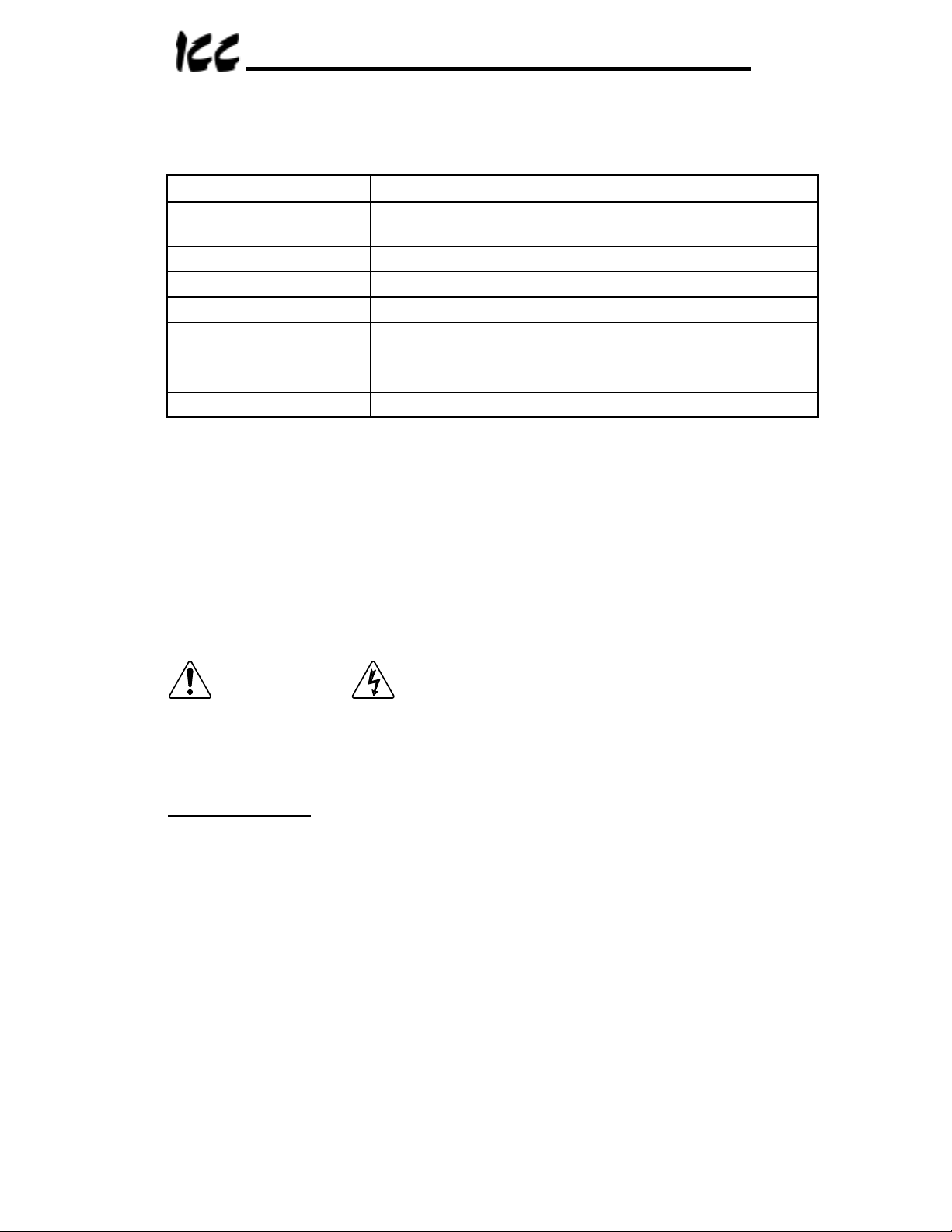
Usage Precautions
Operating Environment
•
Please use the MDB-100 only when the ambient temperature of the environment into
which the MDB-100 is installed is within the following specified temperature limits:
Operation
Storage
•
Avoid installation locations that may be subjected to large shocks or vibrations.
•
Avoid installation locations that may be subjected to rapid changes in temperature or
humidity.
: -10 ∼ +40°C (+14 ∼ +104°F)
: -25 ∼ +65°C (-13 ∼ +149°F)
Installation
•
Do not touch charged parts of the drive such as the terminal block while the drive’s
CHARGE lamp is lit. A charge will still be present in the drive’s internal electrolytic
capacitors, and therefore touching these areas may result in an electrical shock.
Always turn all drive input power supplies OFF, and wait at least 5 minutes after the
CHARGE lamp has gone out before connecting communication cables or motor wiring.
•
Route all communication cables separate from the inverter input/output power wiring.
•
To avoid the possibility of electric shock due to leakage currents, always ground the
inverter unit’s E/GND terminal and the motor. To avoid misoperation, do not connect
the MDB-100’s SHIELD terminal to either of the above-mentioned grounds or any other
power ground.
•
When making connections between the MDB-100 and S7 drives, do not use cables
that exceed 5 meters in length.
•
For further drive-specific precaution, safety and installation information, please refer to
the appropriate Toshiba documentation supplied with your S7 drive.
Other Precautions
•
The drive’s EEPROM has a life span of 10,000 write cycles. Do not write to the same
holding register (other than registers 7A00 ∼ 7A02 and FA00 ∼ FA02 or write-only coils)
more than 10,000 times.
•
The MDB-100’s EEPROM has a life span of 100,000 write cycles. Do not write to the
same MDB-100 configuration register more than 100,000 times.
•
Do not touch or insert a rod or any other item into the MDB-100’s case while power is
applied, as this may lead to electrical shock or device damage.
•
Commission the disposal of the MDB-100 to a specialist.
•
Do not assign the same network address to more than one MDB-100 station in the
same network. For a detailed explanation of station addressing, refer to section 8.
•
When the MDB-100 is configured to receive its Modbus RTU / ASCII station address
from the drive on Channel A, be sure to reset the MDB-100 if the inverter number
parameter on the drive on Channel A is changed. Refer to section 8 for more
information.
•
Because the MDB-100 derives its control power from the drive connected to Channel
A, removing power from that drive will also cause the MDB-100 to lose power, even if
power is still applied to the drive connected to channel B.
•
When only 1 drive is connected to the MDB-100, it must be connected to Channel A.
••••
Wiring
2
Page 4

TABLE OF CONTENTS
1.
2.
3.
4.
5.
6.
6.1 Storage ..........................................................................................................10
6.2 Warranty ........................................................................................................10
7.
8.
9.
9.1 Supported Modbus Commands ......................................................................15
9.2 Programmable Pointer Register Function .......................................................15
9.3 Loss of Communications Timer Function.......................................................16
9.4 Response Delay Timer Function .................................................................... 17
Interface Package Diagram..................................................................4
Feature Summary.................................................................................. 5
Installing The MDB-100 ........................................................................7
Equipment Specifications....................................................................9
Maintenance And Inspection ...............................................................9
Storage And Warranty........................................................................10
Network Characteristics Configuration ............................................11
Modbus Station Address Selection...................................................13
Modicon Programming.......................................................................15
10. Modbus Programming Interface........................................................19
10.1
10.2
10.3
10.4
Overview.....................................................................................................19
Holding Registers .......................................................................................24
Write-Only Coils..........................................................................................31
Read-Only Coils..........................................................................................32
11. Notes....................................................................................................33
3
Page 5
)
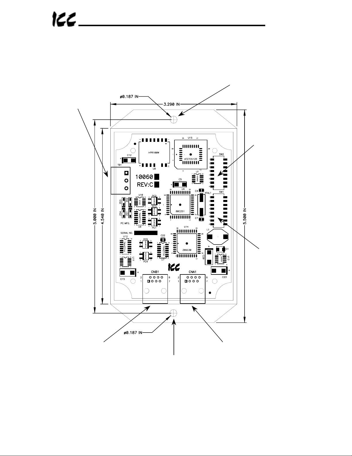
1. Interface Package Diagram
Network connector
(TB1)
Case mounting hole
Switch SW2
(local address)
Switch SW1
(network
characteristics
Drive “B” connector Drive “A” Connector
Case mounting hole
Note that the above diagram shows the MDB-100 with its cover removed. However,
it is only necessary to remove the cover in order to initially configure the MDB-100.
Once configured, the cover should be reinst alled to prevent damage and dust
accumulation.
4
Page 6

2. Feature Summary
The MDB-100 interface provides a wide array of network data access and drive
control features. Combined with the flexible data access methods and universal
acceptance of the Modbus network, this allows powerful networked contr ol and
monitoring systems to be designed. Som e of the main features provided by the
MDB-100 which allow for this control and configurability are briefly described here:
Protocol
Modbus RTU and ASCII as specified in AEG Schneider Automat ion specification
“Modicon Modbus Protocol Reference Guide PI-MBUS-300 Rev. J”.
Implementation
Modbus network is optically isolated RS485 half-duplex 2-wire + shield physical layer,
allowing connection of up to 32 units (masters and slave MDB-100 units) to a single
bus trunk.
Network Baud Rates
Supports all Modbus RTU/ASCII baud rates f rom 300 baud to 38.4kbaud.
Drive Connections
The MDB-100 provides support for simultaneous connection of 2 VF-S7 drives. Both
drives share a common Modbus station address. By supporting 2 drives per
interface, the maximum number of drives that can be connected to 1 Modbus
network segment without requiring r epeat ers increases from 31 (31 drives + 1
master) to 62 (31 MDB-100 units + 1 master).
Power Supply
Self-contained. Powered directly fr om the drive connected to the Channel A
communications port. No external power supply devices or connections are required.
Isolation
The MDB-100 has 3 separate isolated circuitry sections. Each drive is f ully optically
isolated from each other, and bot h dr ives are opt ically isolated from the Modbus
network. By using optically isolated connections to the drives and the Modbus
network, noise immunity is greatly impr oved and g r ounding differential pr oblem s
become a thing of the past.
Drive AutoScan Algorithm
Connections to the drives are automatically established and continuously monitored.
No drive configuration needs to be performed to connect the MDB-100 and
communicate via the Modbus RTU or ASCII network. Just plug it in – it’s that simple.
5
Page 7
Programmable Pointer Registers
32 programmable pointer reg ist ers are provided for user definition. By using these
registers, freq uently-accessed drive parameters that may be scattered throug hout the
register map can be grouped tog ether and accessed with a single holding register
read or write command.
Response Delay Function
A programmable network response delay f unction is available which forces the MDB100 to wait a certain minimum time before generating network responses to Modbus
commands. This function is useful when equipment such as radio modems (which
require a finite time t o switch from receive to transmit mode) are used as Modbus
network bridges.
Network Watchdog
A network watchdog function is available to detect if communication with the master
controller has been interrupted. If an interruption is detected, several different drive
actions can be programmed to ensure that t he pr ocess under control can be safely
and automatically driven to a desired state.
Modbus Network Connector
The network interface is a 3- position pluggable terminal block with the following
signals provided:
Pin Number Function
1 Modbus network RS485 “A” terminal
2 Modbus network RS485 “B” terminal
3 Network shield connection point
No network termination is provided on the MDB-100. Be sure to install proper RS485
network termination on the MDB-100 units that exist on the extreme endpoints of the
network bus. This can be accomplished by placing a 121Ω (±5%) , 1/2W resist or
across the A and B network terminals of t hose 2 unit s .
Drive Network Connectors
Uses standard RJ-45 style 8-pin modular connectors. Any standard category-5
ethernet cable (found in most electronics and office-supply stores) 5 meter s or less in
length can be used to connect the MDB-100 to the drives.
Supported Commands
The MDB-100 presents and receives drive data via Modbus commands 01 (read coil
status), 03 (read holding reg ist er s) , 05 (force single coil), 06 (pr eset single register)
and 16 (preset multiple registers) .
6
Page 8
3. Installing The MDB-100
The MDB-100 connects to each drive via the drive’s communication port, located on
the right-hand side of the dr ive enclosure under a sm all snap- on cover. Although no
drive parameters need to be configur ed in order to use the MDB-100, it is
advantageous to check that the drive’s communicat ion dat a r at e is set to its
maximum speed. Because the MDB-100 will communicate to each drive only at the
drive’s configured data rate, t his will provide the fastest response time for dr ive-t oModbus network data transfers. For information on checking the drive’s
communication data rate, refer to the appropriate manual supplied with your drive.
Note that each drive’s communication data rate settings are independent of the
Modbus network data rate, which is configured solely by the Modbus network
characteristics switch (refer to sect ion 7) . Also not e that the data communication
parameters of each drive are handled independently; the dr ive connected t o Channel
A may simultaneously communicate to the MDB-100 at completely different baud
rates, parity settings, etc. than the drive connected to Channel B.
Installation of the MDB-100 Modbus RTU / ASCII inter face should only be performed
by a qualified technician familiar with the m aintenance and operation of the
connected drives. To install the MDB-100, complete the following steps:
1.
connected have been turned OFF and are locked and tagg ed out .
2.
capacitors to discharge before pr oceeding to the next step.
internal parts with power applied to the drive, or for at least 5 minut es af t er
power to the drive has been removed. A hazard exists temporarily for
electrical shock even if the source power has been removed.
CHARGE LED has gone out before continuing the installation process.
3. Attach the MDB-100 to a sturdy, unmovable object (such as a wall) via the 2 case
mounting holes located on the tabs at the t op and bottom of the enclosure.
4. Remove the drive’s communication port cover, located on the rig ht - hand side of
the drive (as viewed when facing the drive), by pressing against the side of the
cover while sliding it toward the front of the drive. Do not discard this cover, as it
should be reinstalled if the MDB-100 unit is ever disconnected fr om t he drive.
5. Connect the drive’s communication port to Channel A of the MDB-100 with the
communication cable (communication cable is not included with the MDB-100 kit).
When choosing cables for this connection, standard 24 AWG category-5 (CAT 5)
unshielded twisted-pair (UTP) 8-conductor cables f ound in ethernet networks in
most office environments can be used. The maximum allowable length for these
cables is 5 meters. Although there are many varieties and styles of CAT-5 UTP
cables available, ICC strongly recommends using only high- quality cables from
reputable manufacturers to guarantee optimal noise immunity and cable
longevity. Ensure that each end of the cable is fully seated into the modular
connector, and route the cable such that it is locat ed well away from any drive
input power or motor wiring. Also take care to route the cable away from any
sharp edges or positions where it may be pinched.
CAUTION!
DANGER!
Verify that all input power sources to the drives to be
Wait at least 5 minutes for the drive’s electrolytic
Do not touch any
Verify that the
7
Page 9
6. Repeat steps 1, 2, 4 and 5 above to connect another drive to Channel B on the
MDB-100, if desired.
7. Remove the cover of the MDB-100 by removing the 4 cover screws.
8. Configure the Modbus network characteristics such as baud r at e, parity etc. via 8position DIP switch SW1 ( r efer to section 7). If the MDB-100’s station address is
to be configured locally, select the desir ed st ation address via 8-position DIP
switch SW2 (refer to section 8).
9. Reinstall the cover of the MDB-100.
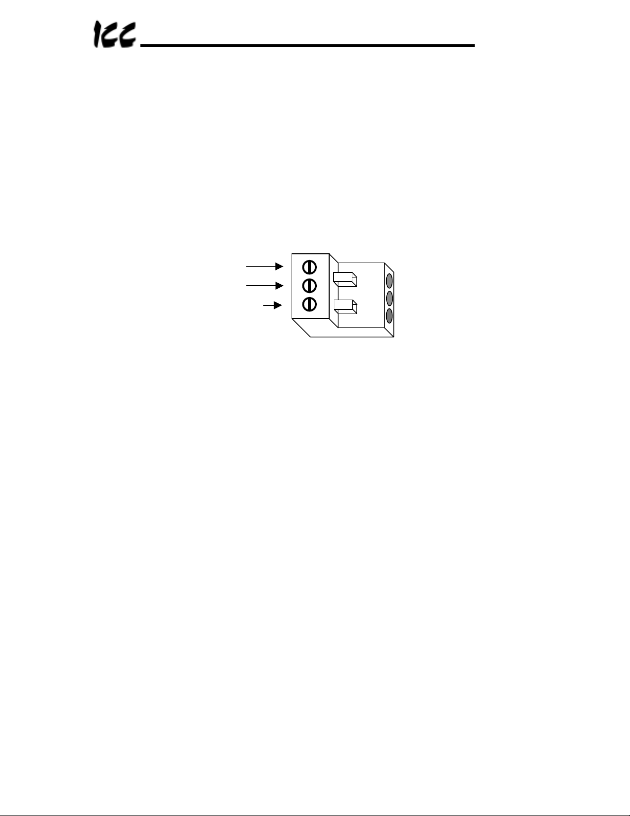
10. Connect the Modbus network cable (2 signal wires + shield) to the 3-position
pluggable terminal block m ar ked “Network” on the left-hand side of the MDB-100.
The terminal ordering for the network cable wiring is as shown in Figure 1.
A
B
SHIELD
Figure 1: Modbus RS485 Network Terminal Wiri ng
Note that some RS485 equipment manufacturers reference t he “ A” and “ B”
terminals reversed from the MDB-100’s hardware, and some manufacturers use
other labels, such as “+” and “-“. If you cannot communicate with the MDB-100
after installation, try switching t he “ A” and “ B” signal wires - swapped signal wires
are the most common cause of communication difficulties in new RS485 network
installations.
Ensure that the Modbus network cable is tightly screwed into the terminals, and
route the cable such that it is located well away from any drive input power or
motor wiring. Also take care to r out e all cables away from any sharp edges or
positions where they may be pinched.
11. Take a moment to verify that the MDB-100 and all network cables have suff icient
clearance from drives, motors , and power-carrying electrical wiring.
12. Turn the power sources to all connected drives ON, and verify that the drives
function properly. If t he dr ives do not appear t o power up, or do not function
properly, immediately turn power OFF.
power from the drives.
Then, verify all connections. Contact ICC or your local
Repeat steps 1 and 2 to remove all
drive distributor or manufacturer for assistance if the problem per sists.
8
Page 10
4. Equipment Specifications
Item Specification
Operating Environment
Operating Temperature
Storage Temperature
Relative Humidity
Vibration
Grounding SHIELD terminal connected to isolated network ground
Cooling Method Self-cooled
Indoors, less than 1000m above sea level, do not
expose to direct sunlight or corrosive / explosive gasses
-10 ∼ +40°C (+14 ∼ +104°F)
-25°C ∼ +65°C (-13 ∼ +149°F)
20% ∼ 90% (without condensation)
5.9m/s
via 200Ω resistance.
2
{0.6G} or less (10 ∼ 55Hz)
5. Maintenance And Inspection
Preventive maintenance and inspection is required to maint ain t he MDB-100 Modbus
interface in its optimal condition and t o ensur e a long operational lifetime. Depending
on usage and operating conditions, perform a periodic inspection once every three to
six months. Before starting inspect ions, always turn off all power supplies to
connected drives, and wait at least five minutes after each drive’s “CHARGE” lamp
has gone out.
DANGER!
to the drives, or for at least 5 minutes after power to the drives has been
removed. A hazard exists temporarily for electrical shock even if the source
power has been removed.
Inspection Points
• Check that the Modbus network connector screws and terminal block plug are not
loose. Tighten if necessary.
• Check that the drive communication cables are not loose. Reinsert if necessary.
• Visually check all wiring and cables for damage. Replace as necessary.
• Clean off any accumulated dust and dirt.
Do not touch any internal parts with power applied
• If use of the MDB-100 is discontinued f or extended per iods of time, apply power
at least once every two years and confirm that the unit still functions properly.
• Do not perform hi-pot t est s on t he drives or MDB-100 interface, as they may
damage the units.
Please pay close attention to all periodic inspection points and maintain a g ood
operating environment.
9
Page 11

6. Storage And Warranty
6.1 Storage
Observe the following points when the MDB-100 interface is not used imm ediat ely
after purchase or when it is not used for an extended per iod of time.
• Avoid storing the MDB-100 in places that are hot or humid, or t hat contain large
quantities of dust or m etallic dust. Store the MDB-100 in a well-ventilated
location.
• When not using the MDB-100 interface for an extended period of time, apply
power at least once every two years and confirm that it still functions properly.
6.2 Warranty
The MDB-100 Modbus RTU / ASCII Communications Interface is covered under
warranty by ICC for a period of 12 months from the date of installat ion, but not to
exceed 18 months from the date of shipm ent from the factory. For further warranty
or service information, please contact Industrial Control Communications or your
local distributor.
10
Page 12
7. Network Characteristics Configuration
The MDB-100 interface board uses an 8-position DIP switch (labeled SW1) to
configure the Modbus network communication characteristics. The switch settings
are only read during initialization, so if a chang e is m ade to any of the switches on
SW1, the MDB-100 must be r eset in order to enable the new settings. The various
configuration setting s of switch SW1 are as follows:
Communication Method:
SW1 #
1
OFF Modbus RTU (factory default)
ON Modbus ASCII
Baud Rate:
4 3 2
OFF OFF OFF 300 baud
OFF OFF ON 600 baud
OFF ON OFF 1200 baud
OFF ON ON 2400 baud
ON OFF OFF 4800 baud
ON OFF ON 9600 baud (factory default)
ON ON OFF 19.2 kbaud
ON ON ON 38.4 kbaud
Parity:
SW1 #
6 5
OFF OFF even parity (factory default)
OFF ON odd parity
ON OFF no parity (2 stop bits)
ON ON no parity (1 stop bit) - applies only to RTU mode
Protocol:
SW1 #
Function
Function
Function
SW1 #
7
OFF Modicon Modbus (factory default)
ON DO NOT SELECT (reserved for future expansion)
Station Number Origin:
SW1 #
8
OFF Drive A’s inverter number parameter (factory default)
ON Switch SW2 address setting
11
(refer to section 8)
Function
Function
Page 13

A Note About Modbus Communicati on Formats
According to the Modicon Modbus Protocol Reference Guide
both Modbus ASCII and RTU communication modes are as f ollows:
ASCII Mode
Coding System:
One hexadecimal character contained in each ASCII character
Bits per Byte:
7 data bits, least signif icant bit sent first
1 bit for even/odd parity; no bit for no parity
1 stop bit if parity is used; 2 bits if no parity
Error Check Field:
RTU Mode
Coding System:
Two hexadecimal characters contained in each 8-bit field of the
Bits per Byte:
8 data bits, least signif icant bit sent first
1 bit for even/odd parity; no bit for no parity
1 stop bit if parity is used; 2 bits if no parity
Error Check Field:
According to the Modicon Modbus specification, theref or e, the number of bits per
byte in ASCII mode is 1 start + 7 data + 1 parity + 1 stop (if parity is used), or 1 start
+ 7 data + 2 stop (if parity is not used). T he ASCII data frame is therefore fixed at 10
bits per byte. Similarly, the number of bit s per byte in RTU mode is 1 start + 8 data +
1 parity + 1 stop (if parity is used), or 1 start + 8 data + 2 stop (if parity is not used),
resulting in an RTU data f r am e that is fixed at 11 bits per byte.
In addition to these standard specified dat a frame sizes, the MDB-100 interface
offers an optional configuration of providing for only 1 stop bit when no parity is
selected in the RTU communication mode. As indicat ed on t he pr evious pag e, by
setting SW5 and SW6 both to “ON”, the RTU data frame size is modified to consist of
1 start + 8 data + 1 stop bit = 10 bits per byte. Please note t hat this setting is only
valid when RTU mode is selected; if SW5 and SW6 ar e both set to “ON” when ASCII
mode is selected, the MDB-100 will halt and will not communicate with the Modbus
network.
...... Hexadecimal, ASCII characters 0 ∼ 9, A ∼ F
of the message
.......... 1 start bit
... Longitudinal Redundancy Check (LRC)
...... 8-bit binary, hexadecimal 0 ∼ 9, A ∼ F
message
.......... 1 start bit
... Cyclical Redundancy Check (CRC)
, the specifications for
12
Page 14

8. Modbus Station Address Selection
The MDB-100 interface provides two differ ent m e t hods for configuring t he node’s
station address. One method uses the inverter num ber parameter read from t he
drive connected to Channel A, and the other method uses a locally-configured
address, set by DIP switches on the MDB-100 control PCB.
When shipped f rom the factory, the MDB-100’s default configuration is to use the
value set in the inverter number parameter (F802) of the drive connected to Channel
A as its Modbus network station address. Depending on the sof tware version of the
drive connected to channel A, this parameter is adjustable from either 0∼31 or 0∼63.
Since Modbus addressing allows for station addresses to be set from 1 ∼ 247,
however, there may be instances where the upper limit of the inverter num ber
parameter setting is not hig h enough to support a desired address (for example, if
you want to set a MDB-100 station to address 95) In these instances, the locallyconfigured station address can be used, which supports the full Modbus station
addressing range of 1 ∼ 247.
Note that the Modbus protocol specification stat es t hat allowable station addresses
are 1 to 247. If a station addr ess is configured with 0 (inverter number or local
address) or 248 to 255 (local address only), the MDB-100 will halt and will not
communicate with the network. To resolve this situat ion, cor rect the station number
and reset the MDB-100. Pay particular attention to this point , as the default factory
setting of the drive’s “inverter number ” parameter is 0, which therefore must be
changed if it is to be used as the MDB-100’s station number .
The selection of whether to use the drive on Channel A’s inverter num ber par am eter
or the locally-set station address is perf or m ed by switch SW1 #8. When SW1 #8 is
OFF (factory default set ting), the MDB-100’s station address is retrieved from drive
A’s inverter number parameter. When SW1 #8 is ON, the MDB-100’s station
address is obtained by the binary number set via DIP switch SW 2 ( factory default
address setting = 1).
SW1 #8 Meaning
OFF
ON
The values of switches SW 1 and SW2 are read only during MDB-100 initialization.
Therefore, if any of these switch settings are changed, the MDB-100 must be
reinitialized to be made aware of the change by:
Drive A’s inverter number parameter (factory default)
Switch SW2 address setting
1. Momentarily powering-off drive A (from which the MDB-100 receives power), or
2. Issuing a reset command to the MDB-100 via the Modbus network by writing to
holding register 0x6111
writing data 0xFEBA will reset the MDB-100 and return all MDB-100 –specific
configuration register s (such as response delay time, loss of communications
timeout time etc.) to t heir factory default values, and writing any other dat a will
cause the MDB-100 to return a Modbus “ILLEGAL DATA VALUE” exception
response (exception code 03). Reading fr om r egister 0x6111 will always return a
value of 0.
13
NOTE 1, NOTE 2
. Wr it ing data 0x5A5A will reset the MDB-100,
Page 15

Holding
Register
0x6111
NOTE 1:
Write Data Meaning
0x5A5A Reset the MDB-100
Reset the MDB-100 and return MDB-100
0xFEBA
configuration regist er s t o factory default
values.
Any other value
Return “ILLEGAL DATA VALUE”
exception
Throughout this document, hexadecimal ( base 16) num ber s will be
represented by a preceding “0x” or by a trailing “H” designator, decimal
(base 10) numbers will be represented by a trailing subscripted “ 10”
designator, and binary (base 2) numbers will be represented by a tr ailing
“B” designator. Binary numbers will always be written with their most
significant bit (MSB) at the left, and their least significant bit (LSB) to the
right (next to the “B”).
For example, 0x6111 = 6111H = 24849
= 0110 0001 0001 0001B.
10
NOTE 2:
The Modbus specification lists two addresses for each holding register (4X
reference) and coil (0X reference). These are ref er r ed to as the
“addressed as” and “known” as values. In all instances, regist er s and
coils are addressed starting at zero; i.e. register 1 is addressed as 0, and
coil 15 is addressed as 14, etc. Throughout this document, all addresses
given for coils and holding register s will be their “ addr essed as” values
unless otherwise specified. In other words, add 1 to the register/coil
address given to obtain its “known as” value. For example, the S7 drive’s
inverter number parameter is 0802H (= 0x0802 = 2050
.) Therefore, this
10
register would be “known as” 2051. Refer to t he Modbus Protocol
Reference Guide for a m or e detailed explanation of this issue.
The station address set via switch SW 2 m ust be set using binary encoding. In this
case, SW2 #1 repr esents bit #0 of the address, and SW2 #8 represents bit #7.
When one of the DIP switches of SW 2 is turned ON, the corresponding address bit is
1, and when one of the switches is turned OFF, the corresponding addr ess bit is 0.
For example, if an address of 169
is desired, the conversion calculation would be
10
performed as follows:
= 0xA9 = 1010 1001B, therefore switches SW2 #1, #4, #6 and #8 should be
169
10
ON, and #2, #3, #5 and #7 should be OFF.
Some more address configurat ion examples (factory default setting = 1) :
Address
(Decimal)
1 (min) 0x01 0000 0001B #1
63 0x3F 0011 1111B
200 0xC8 1100 1000B #4, #7, #8
247 (max) 0xF7 1111 0111B
Address
(Hex)
Address
(Binary)
“ON”
Switches
#1 ∼ #6
#1 ∼ #3, #5 ∼ #8
“OFF”
Switches
#2 ∼ #8
#7, #8
#1 ∼ #3, #5, #6
#4
14
Page 16

9. Modicon Programming
9.1 Supported Modbus Commands
The MDB-100 interface supports 5 Modbus commands: command 1 ( 0x01: r ead coil
status), command 3 (0x03: read holding r egisters), command 5 (0x05: force single
coil), command 6 (0x06: preset single register) and command 16 (0x10: preset
multiple registers). Not all r egisters or coils support all commands (for example,
read-only registers cannot be written to with a command 16). For more information,
refer to section 10. The following limits represent the maximum number of registers
and coils that can be read/written in one packet tr ansact ion:
Command
1 32 coils N/A 32 coils N/A
3 125 registers N/A 61 registers N/A
5 N/A 1 coil only N/A 1 coil only
6 N/A 1 register only N/A 1 register only
16 N/A 123 registers N/A 59 registers
RTU Mode
Read Max
RTU Mode
Write Max
ASCII Mode
Read Max
ASCII Mode
Write Max
9.2 Programmable Pointer Register Function
MDB-100 registers 0x6000 ∼ 0x601F and 0x6080 ∼ 0x609F are used as
programmable pointer and data registers, respectively. Registers 0x6000 ∼ 0x601F
(32 total) are used to define ot her register addresses from which you would like to
read or write, and registers 0x6080 ∼ 0x609F (32 total) are the actual registers used
to access the data located at the register addr esses defined in registers 0x6000 ∼
0x601F. For example, if you would like to continuously read the data from registers
0xFE03, 0xFE04, 0xFE06, and 0xFD00, the standard register configuration would
require 3 read commands to be issued: one reading 2 registers starting at r egister
0xFE03, one reading 1 register starting at register 0xFE06, and one reading 1
register starting at r egister 0xFD00. To conserve network bandwidth and speed
processing time, however, the programm able point er registers can be used to allow
the same information to be accessed, but by only issuing 1 comm and which reads 4
registers.
To configure this function, program as many registers as necessar y (up t o 32) in t he
range 0x6000 ∼ 0x601F with the register numbers of the regist er s you would like to
continuously access. In this example, we would set register 0x6000 to 0xFE03 (the
first register number we want to access), register 0x6001 to 0xFE04, register 0x6002
to 0xFE06, and register 0x6003 to 0xFD00. The data located at t hese dr ive stat us
registers can then be obtained by accessing the corresponding registers in the range
0x6080 ∼ 0x609F (data register 0x6080 corresponds to address register 0x6000,
data register 0x6081 corresponds to address regist er 0x6001, et c. ) Therefore, the 4
registers that are to be monit or ed can now be accessed simply by issuing 1 holding
register read command with a length of 4 starting from reg ist er 0x6080. T he returned
15
Page 17

data will be the data obtained from reg ist er s 0xFE03, 0xFE04, 0xFE06, and 0xFD00
(in that order).
Note that the settings of t he pr ogrammable address registers (0x6000 ∼ 0x601F) are
stored in the MDB-100’s nonvolatile EEPROM. Therefore, do not write t o any of
these registers more than 100,000 t imes. Typically, these registers would only be
written to once, when the interface and Modbus network are fir st commissioned.
When the programmable pointer registers ar e modified, the changes are made
effective in the MDB-100 immediately (the MDB-100 does not need to be r eset for the
changed values to take effect).
9.3 Loss of Communications Timer Function
A configurable "loss of communications" (network watchdog) timer function is
provided, which can detect communication losses and perform cert ain actions if a
valid packet is not received and processed within a set time period.
MDB-100 register 0x6100 sets the loss of communication tim e value (adjustable from
100ms to 60.000s in 1ms increments, f act or y sett ing = 10.000s). If a valid
(exception-free) reception-r esponse or exception- free broadcast does not take place
within this time limit, the timer will expire. If the timer expires, 5 possible actions can
occur for each connected drive, as set by the value of registers 0x6101 and 0xE101
(loss of communications action for drive A and drive B, respectively):
Register
0x6101 / 0xE101
Setting
0 (default) No action: ignore timeout
1 Decelerated stop
2 Coast stop
3 Trip “E” (emergency off)
4 Run a preset speed
When a network t im eout is detected, the timeout action is perf or m ed. When
communications are once again reestablished, the timer function is automatically
reset and will once again begin to monitor network r ecept ions. However, any actions
performed as a result of the timeout occurring will not be reversed by the MDB-100
once communications are reestablished; the Modbus master’s application m ust
explicitly modify the affected condit ions t o fully return the drive to its previous state.
Setting 0 is the default setting; when a communications timeout occurs, no action will
be taken.
For setting 1 (decelerated stop) , the drive will stop in a controlled manner if it was
running. This action clears bit #10 in the select ed dr ive’s comm unicat ion com m and
bit structure (register 0x7A00 / 0xFA00 - also the same data as write-only coil #10 /
#26). Note that the “communication command valid” bit of register 0x7A00 / 0xFA00
(bit #15 of each register, or write-only coil #15 / #31) must already be set by the
master application for this t im eout action to control the drive.
Action Taken Upon Timeout
16
Page 18

For setting 2 (coast stop), the drive will coast stop (free run) if it was running . This
action clears bit #10 in the selected drive’s communication command bit structure
(register 0x7A00 / 0xFA00 - also the same data as write-only coil #10 / #26) and set s
bit #11 (same as coil #11 / #27). Note that t he “communication command valid” bit of
register 0x7A00 / 0xFA00 (bit #15 of each reg ist er , or write-only coil #15 / #31) must
already be set by the master application for this t im eout action to control the drive.
For setting 3 (trip “em er gency off”), the dr ive will trip “E”. This action clears bit #10 in
the selected drive’s communication command bit struct ur e ( r egister 0x7A00 / 0xFA00
- also the same data as write-only coil #10 / #26) and sets bit #12 (same as coil #12 /
#28). Note that in this case the sett ing of the “communication command valid” bit of
register 0x7A00 / 0xFA00 (coil #15 / #31) is irrelevant; t he dr ive will trip regardless of
its value.
Setting 4 (run a preset speed) will modif y the set t ings of bits #0 ∼ #3 of the selected
drive’s communication command bit structure (register 0x7A00 / 0xFA00 - also the
same data as write-only coils #0 ∼ #3 / #16 ∼ #19). The preset speed that is to run is
selected by MDB-100 registers 0x6102 (for drive A) and 0xE102 (for dr ive B). The
possible adjustment range for these registers is 0 ∼ 15, corresponding to “no action”
(0) and each of the drive’s 15 possible preset speeds (1 ∼ 15). Note that the
“communication command valid” and “run/stop” bit s of register 0x7A00 / 0xFA00 (bits
#15 and #10 of each register, or write- only coil #15 & #10 / #31 & #26) m ust already
be set by the master application for t his t im eout action to control the drive.
EXTREME CAUTION WHEN SELECTING THIS SETTING!
there is no possibility of personal injury or equipm ent damage due to the inverter
running at the selected speed, especially with the possibility that network
communications may not be able to be reestablished in a timely fa shion ( depending
on what network condition caused the communications timeout in the first place).
Note that the settings of the timeout time, timeout action and timeout pr eset speed
configuration regist er s are stored in the MDB-100’s nonvolatile EEPROM. Therefore,
do not write to any of these registers mor e t han 100,000 times. Also note that when
the setting of any one of these configuration registers is changed, the MDB-100 must
be reset for the new value to be activated and the change to take effect.
Thoroughly verify that
USE
9.4 Response Delay Timer Function
Register 0x6110 contains the setting f or a r esponse delay timer function. This
function is useful for applications where it may not be desirable for the MDB-100
interface to respond immediat ely to t he net work after a read/write request, such as
when a radio modem that must be switched from receive mode t o t r ansmit mode is
being used.
The response delay timer is adjustable in 1ms increments from 0s to 2.000s (fact or y
setting = 0s). A response delay of 0s means that there is no delay; response packets
will be sent by the MDB-100 as soon as they are available. The delay timer starts
when a complete packet is received by the MDB-100, and a response will not be sent
until the timer has expired (at a minimum). Note that this time value only sets a
minimum response delay value - depending on the quantity and location of r egisters
read / written, much more time m ay actually be req uired before a complete response
is formulated and ready to be returned to the network.
17
Page 19

The response delay timer value is read only upon MDB-100 initialization, requiring
the unit to be reset if the value is chang ed for the new value to take eff ect . This
setting is also non-volatile (written to the MDB-100’s EEPROM). Ther efore, do not
write to this register more than 100, 000 t im es.
18
Page 20

10. Modbus Programming Interface
10.1 Overview
Three types of Modbus data may be accessed via the MDB-100. These are holding
registers (4x reference), read-only coils (0x reference) and write-only coils (0x
reference). In order to access 2 drives within the allocated holding register map
(0x0000 ∼ 0xFFFF), each drive is assigned one half of the register space.
Drive A occupies the area from regist er 0x0000 to 0x7FFF. T his ar ea also contains
several network and drive configuration registers (such as the programmable point er
and data registers, network timeout r egisters, etc.) that reside within the MDB-100
only. The registers which the MDB-100 uses for these funct ions ar e not accessible in
the drive. Currently, these register s ar e unoccupied in t he drive, and therefore no
loss of access to any drive parameters exists. Most of the registers for drive A are
mapped to the exact same “communication number” that they are allocated in the S7
drive by Toshiba. Refer to the VF-S7 Serial Com m unicat ions O ption Manual for a list
of communication numbers. T he only exception to this direct mapping are the
registers that occupy communication numbers larger than 0x8000. For these
parameters, their corresponding Modbus holding registers can be obtained by setting
the MSB (bit #15) of their communicat ion number to 0.
For example, the communication number f or drive A’s bus voltage parameter is
0xFE04 (1111 1110 0000 0100B). Setting bit #15 to 0, we obtain the binary value
0111 1110 0000 0100B, or 0x7E04. Reading from Modbus holding reg ist er 0x7E04
(“known as” 0x7E05), therefor e, will return the bus voltage from drive A.
Drive B occupies the area from regist er 0x8000 to 0xFFFF. T his ar ea also contains
the MDB-100 –specific drive configuration registers that correspond to those
available for drive A. Most of the register s for drive B are not mapped to the exact
same “communication number” that t hey are allocat ed in the S7 drive by Toshiba.
For these parameters, their corresponding Modbus holding registers can be obtained
by setting the MSB (bit #15) of their com m unicat ion num ber to 1.
For example, the communication number f or drive B’s deceleration time #1
parameter is 0x0010 (0000 0000 0001 0000B). Setting bit #15 t o 1, we obtain the
binary value 1000 0000 0001 0000B, or 0x8010. Writing to Modbus holding register
0x8010 (“known as” 0x8011), therefore, will modify the deceleration time #1
parameter for drive B.
The only exception to this mapping modificat ion r equirement for drive B are the
registers that occupy communication numbers larger than 0x8000. For these
parameters, the communication number s given in the VF-S7 Serial Communications
Option Manual correspond exactly to their assigned “addressed as” holding registers
(for example, holding reg ist er 0xFE10 will access the past tr ip #1 value from drive B).
Refer to Figure 2 on page 20 for a graphical representat ion of the holding register
mapping that exists in the MDB-100 Modbus interface.
19
Page 21

Dri v e A Co mm.
Numbers
Figure 2: MDB-100 Holding Register Mappi ng
FFFF
F000
EFFF
E000
DFFF
D000
CFFF
C000
BFFF
B000
AFFF
A000
9FFF
9000
8FFF
8000
7FFF
7000
6FFF
6000
5FFF
5000
4FFF
4000
3FFF
3000
2FFF
2000
1FFF
1000
0FFF
0000
MDB-100
Holding
Registe r Map
MDB-100 registers
Drive B registers
Channel B registers
Drive B registers
Drive B registers
Drive A Registers
Channel A registers
Drive A registers
Drive A registers
Dri v e B Co mm.
Numbers
FFFF
F000
EFFF
E000
DFFF
D000
CFFF
C000
BFFF
B000
AFFF
A000
9FFF
9000
8FFF
8000
7FFF
7000
6FFF
6000
5FFF
5000
4FFF
4000
3FFF
3000
2FFF
2000
1FFF
1000
0FFF
0000
Note: Inaccessible (currently unused) areas are shaded.
20
Page 22

Register #
0000 ∼ 05FF
6000 ∼ 601F
6080 ∼ 609F
6100
6101
6102
6110
6111
6112
6113 ∼ 6FFF
7000 ∼ 7FFF
8000 ∼ E100
E101
E102
E103 ∼ EFFF
F000 ∼ FFFF
Table 1: Holding Register Mapping General Overview
Name / Function
Access drive A
Non-volatile programmable
pointer registers (32 total
available)
Programmable pointer data
registers (each register
corresponds to same one in
6000 ∼ 601F range)
Modbus network loss of
communications timeout time
Modbus network loss of
communications timeout action
for Drive A
Loss of communications preset
speed for Drive A (effective only
when register 6101 is set to 4)
Modbus network response delay
time
Reset/reinitialize MDB-100
interface
MDB-100 firmware
version/revision (read-only)
Access drive A -- -Access drive A communication
numbers F000 ∼ FFFF
Access drive B communication
numbers 0000 ∼ 6100
Modbus network loss of
communications timeout action
for Drive B
Loss of communications preset
speed for Drive B (effective only
when register E101 is set to 4).
Access drive B registers 6103 ∼
6FFF
Access drive B -- --
Factory
Setting
-- --
0000
(all 32)
--
10000
(10.000s)
0
0
0
--
(read always
returns 0)
--
-- --
-- --
0
0
-- --
Adjustment
Any value other than
6000 ∼ 601F or
6080 ∼ 609F
Depends on
registers pointed to
100 ∼ 60000
(0.100s ∼ 60.000s)
0= do nothing
1= decelerated stop
2= coast stop
3= trip “E”
4= run a preset
speed
0 ∼ 2000
(0ms ∼ 2.000s)
0x5A5A: reset only
0xFEBA: return
MDB-100 config
registers to factory
setting values
Version = MSB
Revision = LSB
Same as register
Range
0 ∼ 15
6101
0 ∼ 15
21
Page 23

Sections 10.2 to 10.4 specify the communication num ber → holding register
mappings and coil definitions fo r all cur r ent VF-S7 communication numbers. Note
that the parameters and coils shown are those available at the time of this manual
printing; if new parameters ar e added by the dr ive manufacturer and/or parameter
adjustment limits are modified, etc., this will not affect the operation of the MDB-100
interface. As all available parameters, adjustment ranges etc. are det er mined solely
by the connected drive, and not the MDB-100, future drive firmware versions will
automatically be supported by the MDB-100 with no software upgrades required.
In the case of any discrepancies between the informat ion in t he following tables and
the drive’s documentation, the drive’s documentation should always be followed.
Some other important coil and holding r egister notes:
• Remember that all registers and coils indicated in the following sections are
shown with their “addressed as” coil & register numbers. T hese coil &
register numbers are 1 less than their “ known as” numbers.
• A value indicated by “*” in the following tables indicates that t he set ting is
dependent on the connected drive’s capacity. Refer to the drive’s
documentation for these values.
• If frequency command values (r egisters 0x7A01 / 0xFA01) higher than each
respective drive’s FH or UL parameters are written, the write will be
acknowledged, but the drive will not change its f r equency to this invalid value.
• All writes to holding registers use the drive’s RAM / EEPROM data write (“W”)
command except for registers 0x7A00 ∼ 0x7A02 and 0xFA00 ∼ 0xFA02,
which use the drive’s RAM data write (“P”) command.
• If an attempt is made to access non- existent r egisters or coils, an ILLEGAL
DATA ADDRESS exception (code 02) will be returned.
• If an attempt is made to write invalid data to a register or coil, an ILLEG AL
DATA VALUE exception (code 03) will be returned.
• If a drive connected to the MDB-100 goes “offline”, all coils will hold their last
state, with the exception of read-only coils #115 and/or #131, which will
indicate “offline”. O nce communication with the drive(s) is reestablished,
these coil(s) will again indicate “online”.
• If a drive connected to the MDB-100 goes “of fline”, attempts to access any
register in that drive’s regist er space will return a Modbus “SLAVE FAILURE”
error (code 04), except for t he following registers, which will hold their last
state:
1. Communication command (communication number FA00)
2. Communication frequency command (communication number FA01)
3. Output frequency (comm unication number FD00)
4. Status (communication number FE01)
5. Output current (communicat ion num ber FE03)
6. Output voltage (communication num ber FE05)
• Note that the MDB-100 does not assign drive register and coil functions; they
are entirely drive-dependent, and managed by the drive manuf acturer.
• Each drive’s write-only coils are mapped to the corresponding drive’s
communication command parameter (com munication number #FA00). Also,
22
Page 24

the MDB-100 does not place any restrictions on coils marked as “Reserved”.
These coils may be written to at any time. The data or function associated
with these coils is entirely defined by the connected drive.
• With the exception of coils #115 and #131, each drive’s read-only coils are
mapped to the corresponding drive’s communication stat us register
(communication number #FE01). Also, t he MDB-100 does not place any
restrictions on coils marked as “Reserved”. These coils may be read from at
any time. The data or function associated with these coils is ent irely defined
by the connected drive.
23
Page 25

10.2 Holding Registers
Drive
A
B
A
B
A
B
A
B
A
B
A
B
A
B
A
B
A
B
A
B
A
B
A
B
A
B
A
B
A
B
A
B
A
B
A
B
A
B
A
B
A
B
A
B
A
B
Reg. #
(hex)
0000
8000
0001
8001
0002
8002
0003
8003
0004
8004
0005
8005
0006
8006
0007
8007
0008
8008
0009
8009
0010
8010
0011
8011
0012
8012
0013
8013
0014
8014
0015
8015
0016
8016
0017
8017
0018
8018
0019
8019
0020
8020
0021
8021
0022
8022
Title Function
Automatic acceleration and
AU1
deceleration time
AU2
Automatic torque boost 3 0 No
Automatic environment
AU3
setting
CMOD
FMOD
FMSL
Command mode selection 1 0 Yes
Frequency setting mode
selection
FM terminal function
selection
FM
Connected meter adjustment FF:255 0 Yes
Standard setting mode
tYP
selection
Forward/reverse selection
Fr
(panel)
ACC
Acceleration time #1 (s) 8CA0:3600 A:1.0 Yes
dEC
Deceleration time #1 (s) 8CA0:3600 A:1.0 Yes
FH
Maximum frequency 7D00:320.0 BB8:30.0 No
UL
Upper limit frequency
LL
Lower limit frequency
vL
Base frequency 7D00:320.0 9C4:25.0 Yes
Pt
V/F pattern 3 0 No
vb
Voltage boost BB8:30.0 0 Yes
OLM
OL selection 7 0 Yes
Sr1
Preset speed 1
Sr2
Preset speed 2
Sr3
Preset speed 3
Sr4
Preset speed 4
Sr5
Preset speed 5
Max
(hex:dec)
1 0 Yes
2 0 No
2 0 Yes
1 0 Yes
6 0 No
1 0 Yes
FH
UL
UL LL
UL LL
UL LL
UL LL
UL LL
Min
(hex:dec)
32:0.5 Yes
0:0.0 Yes
Run Mode
Modify
Yes
Yes
Yes
Yes
Yes
24
Page 26

Drive
A
B
A
B
A
B
A
B
A
B
A
B
A
B
A
B
A
B
A
B
A
B
A
B
A
B
A
B
A
B
A
B
A
B
A
B
A
B
A
B
A
B
A
B
A
B
A
B
A
B
Reg. #
(hex)
0023
8023
0024
8024
0100
8100
0101
8101
0102
8102
0103
8103
0104
8104
0110
8110
0111
8111
0112
8112
0113
8113
0114
8114
0115
8115
0130
8130
0131
8131
0200
8200
0201
8201
0202
8202
0203
8203
0204
8204
0210
8210
0211
8211
0212
8212
0213
8213
0240
8240
Title Function
Sr6
Preset speed 6
Sr7
Preset speed 7
F100
F101
F102
F103
F104
F110
F111
F112
F113
F114
F115
F130
F131
F200
F201
F202
F203
F204
F210
F211
F212
F213
F240
Low speed signal output
frequency
Speed reach signal output
frequency
Speed reach detection band
ST signal selection 2 0 Yes
RST signal selection 1 0 Yes
Always active function
selection
Input terminal selection #1 25:37 0 Yes
Input terminal selection #2 25:37 0 Yes
Input terminal selection #3 25:37 0 Yes
Input terminal selection #4 25:37 0 Yes
Input terminal selection #5 25:37 0 Yes
Output terminal selection #1 9 0 Yes
Output terminal selection #2 9 0 Yes
Frequency priority selection 1 0 Yes
VIA reference point #1 64:100 0 Yes
VIA point #1 frequency 7D00:320.0 0:0.0 Yes
VIA reference point #2 64:100 0 Yes
VIA point #2 frequency 7D00:320.0 0:0.0 Yes
VIB reference point #1 64:100 0 Yes
VIB point #1 frequency 7D00:320.0 0:0.0 Yes
VIB reference point #2 64:100 0 Yes
VIB point #2 frequency 7D00:320.0 0:0.0 Yes
Start-up frequency 3E8:10.0 32:0.5 Yes
Max
(hex:dec)
UL LL
UL LL
FH
FH
FH
25:37 0 Yes
Min
(hex:dec)
0:0.0 Yes
0:0.0 Yes
0:0.0 Yes
Run Mode
Modify
Yes
Yes
25
Page 27

Drive
A
B
A
B
A
B
A
B
A
B
A
B
A
B
A
B
A
B
A
B
A
B
A
B
A
B
A
B
A
B
A
B
A
B
A
B
A
B
A
B
A
B
A
B
A
B
A
B
A
B
Reg. #
(hex)
0241
8241
0242
8242
0250
8250
0251
8251
0252
8252
0260
8260
0261
8261
0270
8270
0271
8271
0272
8272
0273
8273
0274
8274
0275
8275
0280
8280
0281
8281
0282
8282
0283
8283
0284
8284
0285
8285
0286
8286
0287
8287
0288
8288
0289
8289
0290
8290
0291
8291
Title Function
F241
F242
F250
F251
F252
F260
F261
F270
F271
F272
F273
F274
F275
F280
F281
F282
F283
F284
F285
F286
F287
F288
F289
F290
F291
Run frequency
Run frequency hysteresis
DC injection starting
frequency
DC injection current 64:100 0 Yes
DC injection time C8:20.0 0:0.0 Yes
Jog run frequency 7D0:20.0 0:0.0 Yes
Jog stop control 2 0 Yes
Jump frequency #1
Jump frequency band #1 BB8:30.0 0:0.0 Yes
Jump frequency #2
Jump frequency band #2 BB8:30.0 0:0.0 Yes
Jump frequency #3
Jump frequency band #3 BB8:30.0 0:0.0 Yes
Preset speed 1
Preset speed 2
Preset speed 3
Preset speed 4
Preset speed 5
Preset speed 6
Preset speed 7
Preset speed 8
Preset speed 9
Preset speed 10
Preset speed 11
Preset speed 12
Max
(hex:dec)
FH
FH
FH
UL LL
UL LL
UL LL
UL LL
UL LL
UL LL
UL LL
UL LL
UL LL
UL LL
UL LL
UL LL
UL LL
UL LL
UL LL
Min
(hex:dec)
0:0.0 Yes
0:0.0 Yes
0:0.0 Yes
Run Mode
Modify
Yes
Yes
Yes
Yes
Yes
Yes
Yes
Yes
Yes
Yes
Yes
Yes
Yes
Yes
Yes
26
Page 28

Drive
A
B
A
B
A
B
A
B
A
B
A
B
A
B
A
B
A
B
A
B
A
B
A
B
A
B
A
B
A
B
A
B
A
B
A
B
A
B
A
B
A
B
A
B
A
B
A
B
Reg. #
(hex)
0292
8292
0293
8293
0294
8294
0300
8300
0301
8301
0302
8302
0303
8303
0304
8304
0305
8305
0306
8306
0307
8307
0400
8400
0401
8401
0402
8402
0403
8403
0404
8404
0405
8405
0406
8406
0407
8407
0500
8500
0501
8501
0502
8502
0503
8503
0504
8504
Title Function
F292
F293
F294
F300
F301
F302
F303
F304
F305
F306
F307
F400
F401
F402
F403
F404
F405
F406
F407
F500
F501
F502
F503
F504
Preset speed 13
Preset speed 14
Preset speed 15
PWM carrier frequency (kHz) * 16:2.2 Yes
Auto-restart (motor speed
search)
Regeneration power ridethrough control
Retry selection: number of
times
Regenerative braking
selection
Overvoltage stall protection 1 0 Yes
Output voltage adjustment 78:120 0 Yes
Line voltage compensation 1 0 No
Auto-tuning 2 0 No
Slip frequency gain FF:255 0 Yes
Motor constant 1: R1 gain FF:255 0 No
Motor constant 2: R2 gain FF:255 0 No
Motor constant 3: M gain FF:255 0 No
Load inertia 3 0 Yes
Auto torque boost no load
current
Auto torque boost maximum
boost
Acceleration time #2 8CA0:3600 1:0.1 Yes
Deceleration time #2 8CA0:3600 1:0.1 Yes
Acceleration & deceleration
pattern #1
Acceleration & deceleration
pattern #2
Acceleration & deceleration
pattern #1 & #2
Max
(hex:dec)
UL LL
UL LL
UL LL
3 0 Yes
1 0 Yes
A:10 0 Yes
1 0 Yes
1E:30 0 Yes
1E:30 0 Yes
2 0 Yes
2 0 Yes
1 0 Yes
Min
(hex:dec)
Run Mode
Modify
Yes
Yes
Yes
27
Page 29

Drive
A
B
A
B
A
B
A
B
A
B
A
B
A
B
A
B
A
B
A
B
A
B
A
B
A
B
A
B
A
B
A
B
A
B
Reg. #
(hex)
0505
8505
0600
8600
0601
8601
0602
8602
0603
8603
0604
8604
0605
8605
0700
8700
0701
8701
0702
8702
0800
8800
0801
8801
0802
8802
0803
8803
7A00
FA00
7A01
FA01
7A02
FA02
Title Function
Acceleration & deceleration
F505
F600
F601
F602
F603
F604
F605
F700
F701
F702
F800
F801
F802
F803
FA00
FA01
FA02
pattern #1 & #2 switching
frequency
Motor overload protection
level
Stall protection level C8:200 * Yes
Fault trip saving 1 0 Yes
Emergency stop selection 2 0 Yes
Emergency stop DC injection
time
Open phase detection
parameter
Parameter setting disable
selection
Unit selection 3 0 Yes
Frequency units
multiplication factor
Communication speed 3 0 Yes
Parity 2 0 Yes
Inverter number 1F:31 0 Yes
Communication error trip
time
Communication command FFFF:65535 0 Yes
Communication frequency
command
Panel frequency command
Max
(hex:dec)
UL
64:100 * Yes
C8:20.0 0:0.0 Yes
2 0 Yes
2 0 Yes
4E20:200.0 64:0.01 Yes
64:100 0 Yes
FH
FH
Min
(hex:dec)
0:0.0 Yes
0:0.0 Yes
0:0.0 Yes
Run Mode
Modify
28
Page 30

Status Monitoring Parameters (read-only)
Drive
A
B
A
B
A
B
A
B
A
B
A
B
A
B
A
B
A
B
A
B
A
B
A
B
A
B
A
B
A
B
A
B
Comm #
(hex)
7D00
FD00
7E00
FE00
7E01
FE01
7E02
FE02
7E03
FE03
7E04
FE04
7E05
FE05
7E06
FE06
7E07
FE07
7E08
FE08
7E09
FE09
7E10
FE10
7E11
FE11
7E12
FE12
7E13
FE13
7E14
FE14
Function
Current output frequency
Output Frequency (saves trip
frequency)
Status (saves trip status)
Current frequency command
Output current display
Bus voltage
Output voltage
Input terminal data
Output terminal data
CPU version
EEPROM version
Past trip 1
Past trip 2
Past trip 3
Past trip 4
Cumulative run time
29
Page 31

Trip Data Codes
Display Data Trip Type
nErr
OC1
OC2
OC3
OCL
OCA
EPH1
EPH0
OP1
OP2
OP3
OL1
OL2
OLr
OH
E
EEP1
Err2
Err3
Err4
Err5
OCr
Etn
EtYP
0000 No trip
0001 Overcurrent during acceleration
0002 Overcurrent during deceleration
0003 Overcurrent during constant-speed run
0004 Load-end short circuit trip during star t-up
0005 Phase short circuit
0006 reserved
0007 reserved
0008 reserved
0009 Loss of output phase
000A Overvoltage during acceleration
000B Overvoltage during deceleration
000C Overvoltage during constant-speed run
000D Inverter overload trip
000E Motor overload trip
000F DBR overload
0010 Overheat trip
0011 Emergency stop
0012 EEPROM fault: write error
0013 reserved
0014 reserved
0015 RAM fault
0016 ROM fault
0017 CPU fault
0018 Communication interruption error
0019~0024 reserved
0025 Dynamic braking resistor trip
0026~0027 reserved
0028 Auto-tuning error
0029 Inverter typeform error
30
Page 32

10.3 Write-Only Coils
Coil # S7 ASD Function OFF ON
31 Command source Local Network
30 Frequency command source Local Network
29 Fault reset N/A Reset
28 Emergency OFF command N/A Trip “E”
27 Coast stop command N/A Coast stop
26 Run / stop command Stop Run
25 Forward / reverse selection Forward Reverse
24 Jog command N/A Jog
23
Drive B
22 Accel / decel #1/#2 selection #1 #2
21 Reserved -- -20 Reserved -- -19 Preset speed 4 OFF ON
18 Preset speed 3 OFF ON
17 Preset speed 2 OFF ON
16 Preset speed 1 OFF ON
15 Command source Local Network
14 Frequency command source Local Network
13 Fault reset N/A Reset
12 Emergency OFF command N/A Trip “E”
11 Coast stop command N/A Coast stop
10 Run / stop command Stop Run
9 Forward / reverse selection Forward Reverse
8 Jog command N/A Jog
7
Drive A
6 Accel / decel #1/#2 selection #1 #2
5 Reserved -- -4 Reserved -- -3 Preset speed 4 OFF ON
2 Preset speed 3 OFF ON
1 Preset speed 2 OFF ON
0 Preset speed 1 OFF ON
DC injection braking N/A
DC injection braking N/A
DC injection
command
DC injection
command
31
Page 33

10.4 Read-Only Coils
Coil # S7 ASD Function OFF ON
131 Drive B online / offline status Offline Online
130 Reserved Always “0”
129 Reserved Always “0”
128 Reserved Always “0”
127 Reserved Always “0”
126 Run / stop status Stopped Running
125 Forward / reverse status Forward Reverse
124 Jog status Not jogging Jogging
123
DC injection braking status
Drive B
122 Accel / decel #1/#2 status #1 #2
121 Reserved Always “0”
120 Reserved Always “0”
119 Reserved Always “0”
118 Reserved Always “0”
117 Reserved Always “0”
116 Reserved Always “0”
115 Drive A online / offline status Offline Online
114 Reserved Always “0”
113 Reserved Always “0”
112 Reserved Always “0”
111 Reserved Always “0”
110 Run / stop status Stopped Running
109 Forward / reverse status Forward Reverse
108 Jog status Not jogging Jogging
107
DC injection braking status
Drive A
106 Accel / decel #1/#2 status #1 #2
105 Reserved Always “0”
104 Reserved Always “0”
103 Reserved Always “0”
102 Reserved Always “0”
101 Reserved Always “0”
100 Reserved Always “0”
Not DC injection
braking
Not DC injection
braking
DC injection
DC injection
braking
braking
32
Page 34

11. Notes
33
Page 35

34
Page 36

35
Page 37

36
Page 38

W
2202 Timberloch Place, Suite 210
The Woodlands, TX USA 77380-1163
Tel: [281] 367-3007 Fax: [281] 367-2177
orld Wide Web http://www.iccdesigns.com
Printed in U.S.A
 Loading...