

Page 1

SERVICE MANUAL
DOCUMENT CREATED IN JAPAN, Oct., 2003
DIGITAL VIDEO
DVD VIDEO RECORDER
FILE NO. 810-200334
D-R1SU
D-R1SC
Page 2
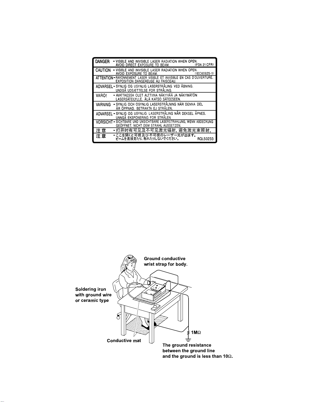
LASER BEAM CAUTION LABEL
When the power supply is being turned on, you may not remove this laser beam caution label. If it removes, radiation of a
laser may be received.
PREPARATION OF SERVICING
Pickup Head consists of a laser diode that is very susceptible to external static electricity.
Although it operates properly after replacement, if it was subject to electrostatic discharge during replacement,
its life might be shortened. When replacing, use a conductive mat, soldering iron with ground wire, etc. to
protect the laser diode from damage by static electricity.
And also, the LSI and IC are same as above.
Ground conductive
wrist strap for body.
Soldering iron
with ground wire
or ceramic type
Conductive mat
1M
W
The ground resistance
between the ground line
and the ground is less than 10W.
Page 3
SAFETY NOTICE
SAFETY PRECAUTIONS
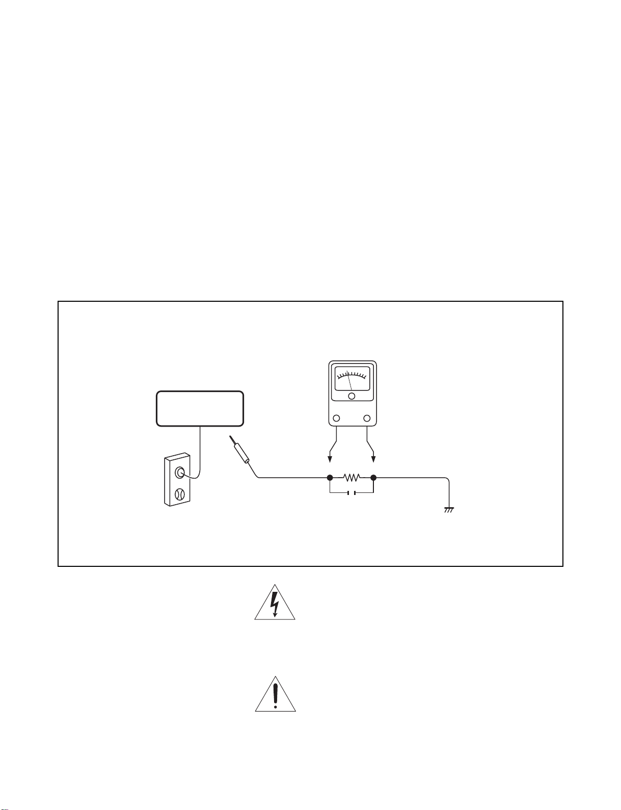
LEAKAGE CURRENT CHECK
Plug the AC line cord directly into a 120V AC outlet (do
not use an isolation transformer for this check). Use an
AC voltmeter, having 5000 Ω per volt or more sensitivity.
Connect a 1500 Ω 10 W resistor, paralleled by a 0.15 µF
150V AC capacitor between a known good earth ground
(water pipe, conduit, etc.) and all exposed metal parts of
cabinet (antennas, handle bracket, metal cabinet
screwheads, metal overlays, control shafts, etc.).
READING SHOULD NOT EXCEED 0.3V
Measure the AC voltage across the 1500 Ω resistor.
The test must be conducted with the AC switch on and
then repeated with the AC switch off. The AC voltage
indicated by the meter may not exceed 0.3 V. A reading
exceeding 0.3 V indicates that a dangerous potential
exists, the fault must be located and corrected.
Repeat the above test with the DVD VIDEO RECORDER
power plug reversed.
NEVER RETURN A DVD VIDEO RECORDER TO THE
CUSTOMER WITHOUT TAKING NECESSARY
CORRECTIVE ACTION.
DVD VIDEO RECORDER
AC OUTLET
Test all exposed metal.
Voltmeter Hook-up for Leakage Current Check
AC VOLTMETER
(5000 Ω per volt
or more sensitivity)
Good earth ground
such as a water pipe,
1500 Ω
10 W
0.15 µF 150V AC
conduit, etc.
The lightning flash with arrowhead symbol, within an
equilateral triangle, is intended to alert the user to the
presence of uninsulated “dangerous voltage” within the
product’s enclosure that may be of sufficient magnitude to
constitute a risk of electric shock to persons.
The exclamation point within an equilateral triangle is
intended to alert the user to the presence of important
operating and maintenance (servicing) instructions in the
literature accompanying the appliance.
Page 4

1. OPERATING INSTRUCTIONS
CONTENTS
SECTION 1
GENERAL DESCRIPTIONS
2. LOCATION OF MAIN PARTS
2-1. Location of Main Parts
2-2. Location of PC Boards
PART REPLACEMENT AND ADJUSTMENT PROCEDURES
1. REPLACEMENT OF MECHANICAL PARTS
1-1. Cabinet Replacement
1-1-1. Top Cover
1-1-2. Front Panel
1-1-3. Tray Door
1-1-4. RAM Drive
1-1-5. Fan
1-1-6. Rear Panel
1. CIRCUIT SYMBOLS AND
SUPPLEMENTARY EXPLANATION
1-1. Circuit Symbols
1-2. Precautions for Part Replacement
2. PRINTED WIRING BOARD AND
SCHEMATIC DIAGRAM
3. BLOCK DIAGRAMS
3-1. Overall Block Diagram
4. CIRCUIT DIAGRAMS
4-1. Power Supply Circuit Diagram
4-2. Front Circuit Diagram
4-2-1. Front (Jack) Circuit Diagram
4-2-2. Front (L) Circuit Diagram
4-2-3. Front (R) Circuit Diagram
SECTION 2
1-2. PC Board Replacement
1-2-1. Digital PC Board
1-2-2. Mother PC Board
1-2-3. Power PC Board
1-2-4. Front (R), Front (L) and Jack PC Board
SECTION 3
SERVICING DIAGRAMS
4-3. Digital Circuit Diagram
4-3-1. Digital 1 Circuit Diagram
4-3-2. Digital 2 Circuit Diagram
4-4. Mother Circuit Diagram
4-4-1. Tuner Circuit Diagram
4-4-2. Timer Circuit Diagram
4-4-3. Audio Circuit Diagram
4-4-4. Video Circuit Diagram
5. PC BOARDS
5-1. Front (L) PC Board
5-2. Front (R) PC Board
5-3. Front (Jack) PC Board
5-4. Digital PC Board
5-5. Mother PC Board
SAFETY PRECAUTION
NOTICE
ABBREVIATIONS
1. Integrated Circuit (IC)
2. Capacitor (Cap)
3. Resistor (Res)
SECTION 4
PARTS LIST
4. EXPLODED VIEWS
4-1. Packing Assembly
4-2. Chassis Assembly
5. PARTS LIST
Page 5

GENERAL DESCRIPTIONS
SECTION 1
GENERAL DESCRIPTIONS
1. OPERATING INSTRUCTIONS
Please refer to the owner's manual about the contents.
SECTION 1
Page 6
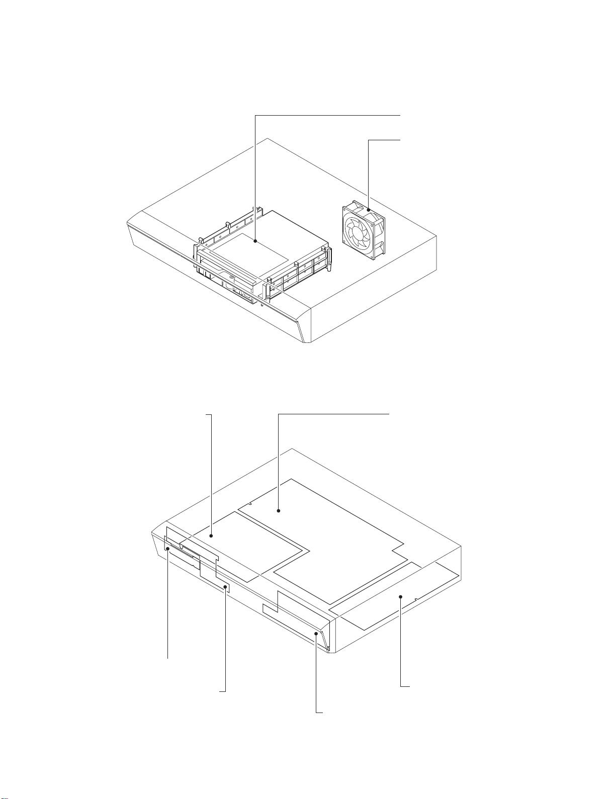
2. LOCATION OF MAIN PARTS
2-1. Location of Main Parts
RAM1 RAM DRIVE
ZG45 FAN
Fig. 1-2-1
2-2. Location of PC Boards
EU01 Digital PC board
EU55 Jack PC board
EU05 Mother PC board
EU03B Front (L) PC board
EU02 Power PC board
EU03A Front (R) PC board
Fig. 1-2-2
Page 7
SECTION 2
PART REPLACEMENT AND
ADJUSTMENT PROCEDURES
CAUTIONS BEFORE STARTING PART REPLACEMENT
Electronic parts are susceptible to static electricity and may be easily damaged, so do not forget to ground as required.
Many screws are used inside the unit. To prevent the screws from missing or dropping, etc. always use a magnetized
screwdriver in servicing. Several kinds of screws are used and some of them need special cautions. That is, take care of
the tapping screws securing molded parts and fine pitch screws used to secure metal parts. If they are used improperly,
the screw holes will be easily damaged and the parts can not be fixed.
1. REPLACEMENT OF MECHANICAL PARTS
ADJUSTMENT PROCEDURES
PART REPLACEMENT AND
1-1. Cabinet Replacement
1-1-1. Top Cover
(1) Remove seven screws (1), and then remove the top cover (2).
Screws (1)
Top cover (2)
SECTION 2
Screws (1)
Screws (1)
Fig. 2-1-1
Page 8
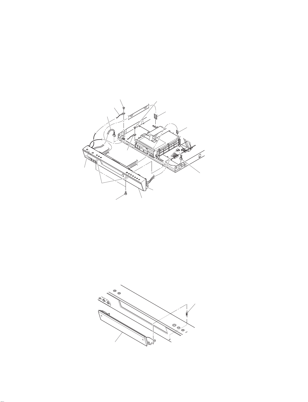
1-1-2. Front Panel
(1) Remove the top cover. (Refer to item 1-1-1.)
(2) Disconnect the flexible cable (1).
(3) Disconnect the flexible cable (2) and two connectors (3).
(4) Remove two screws (4) and two ground wires (5) and (6).
(5) Release four claws and remove two screws (7).
(6) Remove the front panel (8).
Screw (4)
Ground wire (6)
Connector (3)
Ground
wire (5)
Claw
Claws
Screws (7)
Screw (4)
Claw
Front panel (8)
Fig. 2-1-2
1-1-3. Tray Door
(1) Remove the front panel. (Refer to item 1-1-2.)
(2) Remove the Front (R) PC board. (Refer to item 1-2-4 (2) to (4).)
(3) Remove the spring (1).
(4) Remove the tray door (2) while slightly bending it.
Flexible cable (1)
Flexible cable (2)
Connector (3)
Tray door (2)
Spring (1)
Fig. 2-1-3
Page 9
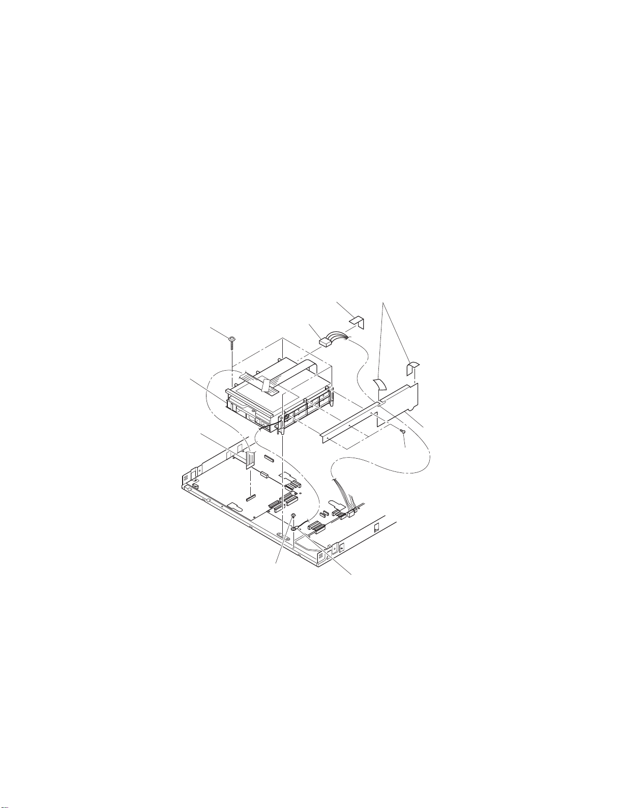
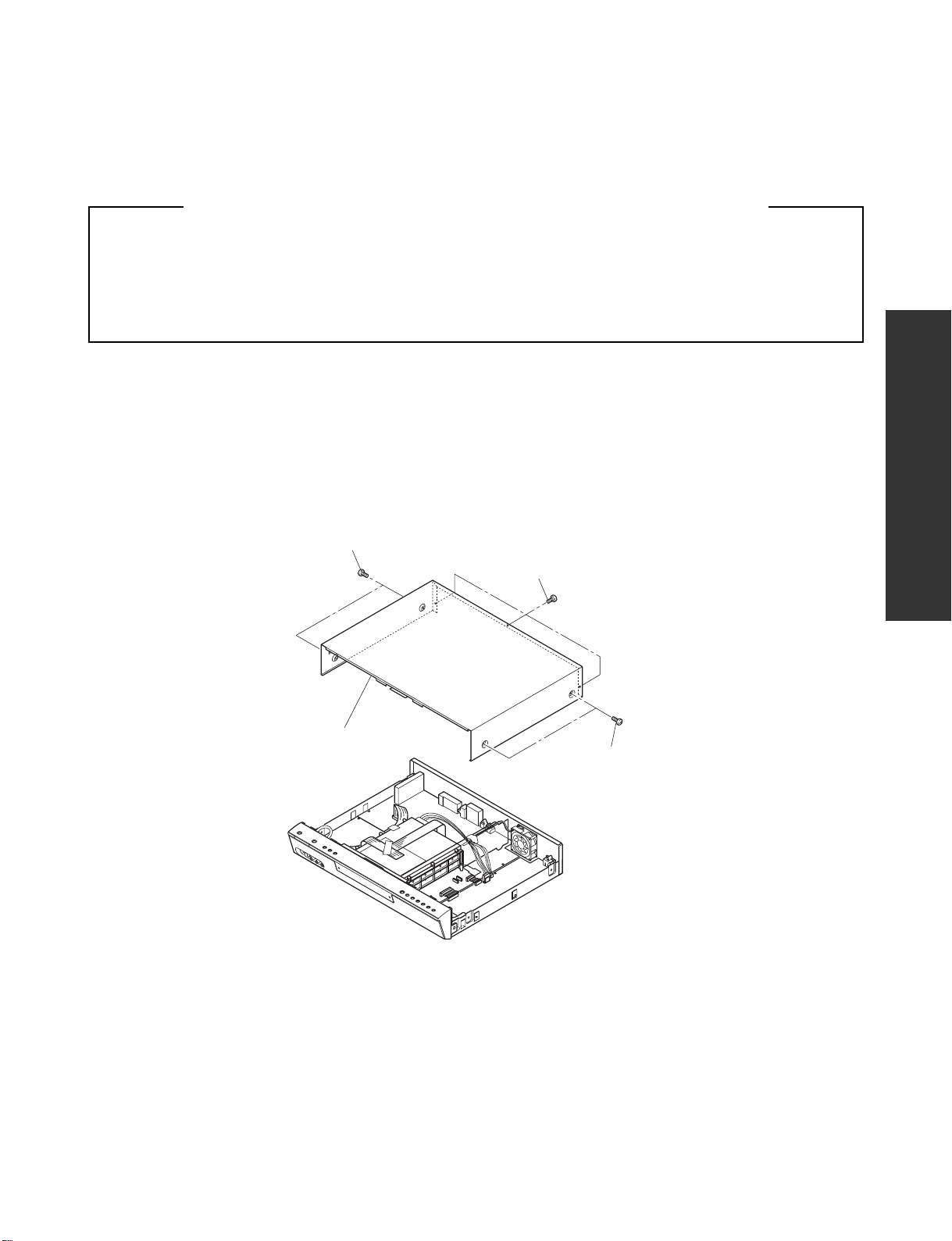
1-1-4. RAM Drive
(1) Remove the top cover. (Refer to item 1-1-1.)
(2) Remove the front panel. (Refer to item 1-1-2.)
(3) Disconnect the flexible cable (1).
(4) Remove the piece of tape (2).
(5) Disconnect the connector (3).
(6) Remove two pieces of tape (4).
(7) Remove three screws (5), and then remove the acrylic board (6).
(8) Remove the screw (7) and the ground wire (8).
(9) Remove four screws (9), and then remove the RAM drive (10).
(Note)
After replacing, tape on three points of (2) and (4) as they were.
Screws (9)
RAM drive (10)
Flexible cable (1)
Connector (3)
Screw (7)
Tape (2)
Tape (4)
Acrylic board (6)
Screws (5)
Ground wire (8)
Fig. 2-1-4
Page 10
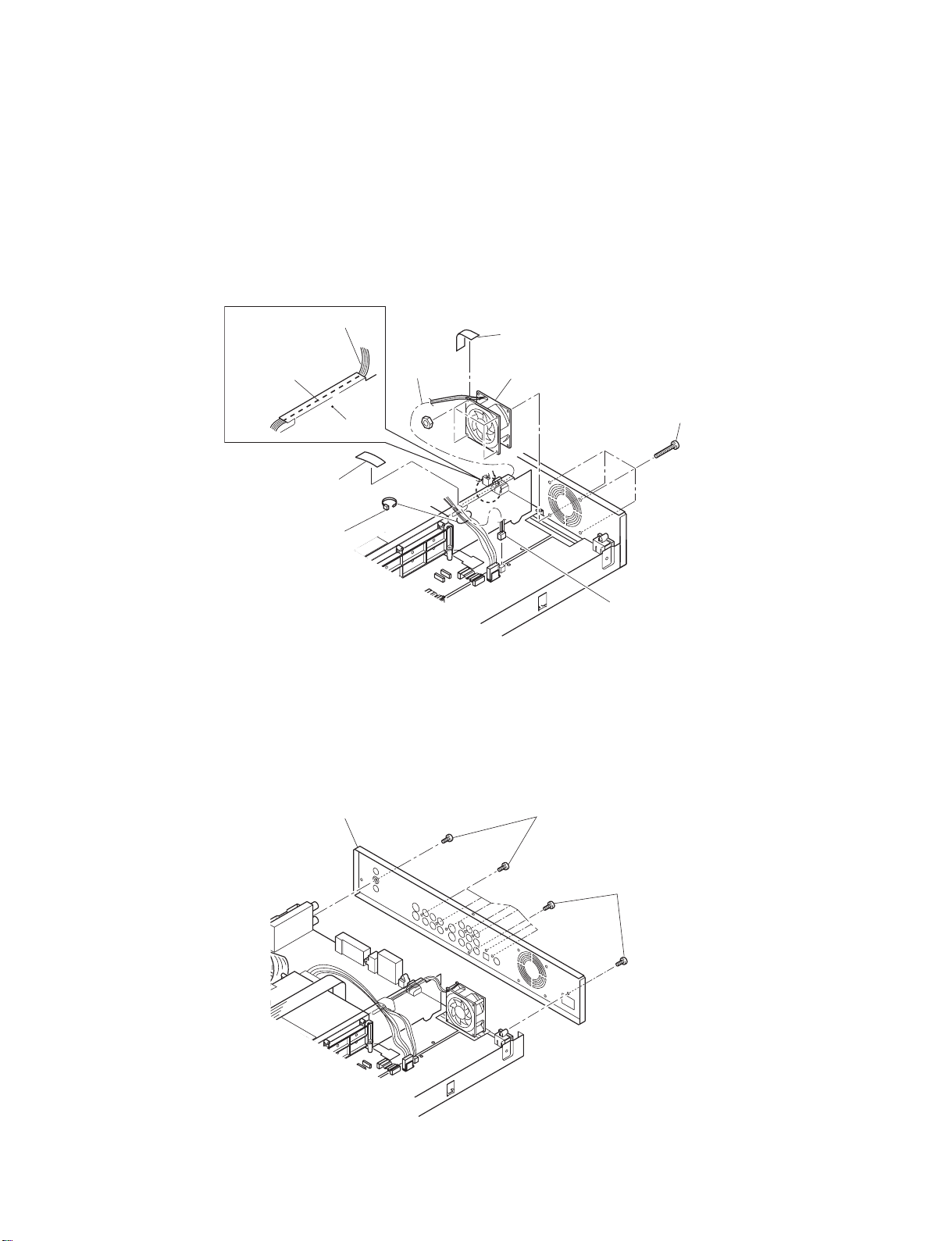
1-1-5. Fan
(1) Remove the two pieces of tape (1).
(2) Cut off the binding band (2).
(3) Disconnect the connector (3).
(4) Remove four screws (4), and then remove the fan (5).
(Note)
• After replacing, tape on two points (1) as they were.
• Pass the wire (6) underneath the folded part of the acrylic board.
Lead wire (6)
Pass the lead (6)
underneath the
folded porton
Acrylic board
Tape (1)
Binding band (2)
1-1-6. Rear Panel
(1) Remove the fan. (Refer to 1-1-5.)
(2) Remove ten screws (1) and the rear panel (2).
Fan (6)
Tape (1)
Fan (5)
Screws (4)
Connector (3)
Fig. 2-1-5
Rear panel (2)
Screws (1)
Screws (1)
Fig. 2-1-6
Page 11
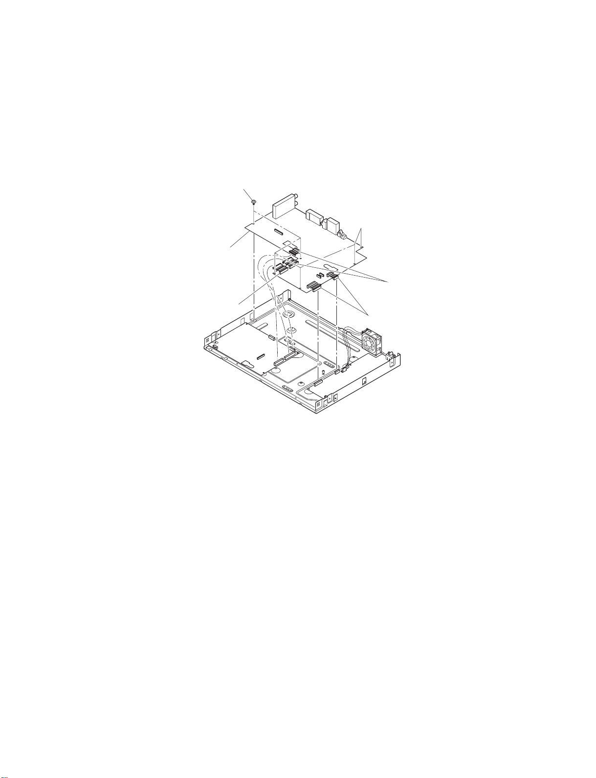
1-2. PC Board Replacement
1-2-1. Digital PC Board
(1) Remove the front panel. (Refer item to 1-1-2.)
(2) Remove the RAM drive. (Refer item to 1-1-4.)
(3) Disconnect three connectors (1).
(4) Remove the screw (2) to remove the ground wire (3).
(5) Remove four screws (4), and then remove the digital PC board (5).
Screws (4)
Connector (1)
Digital PC board (5)
Fig. 2-1-7
Connector (1)
Connector (1)
Screw (2)
Ground wire (3)
Page 12
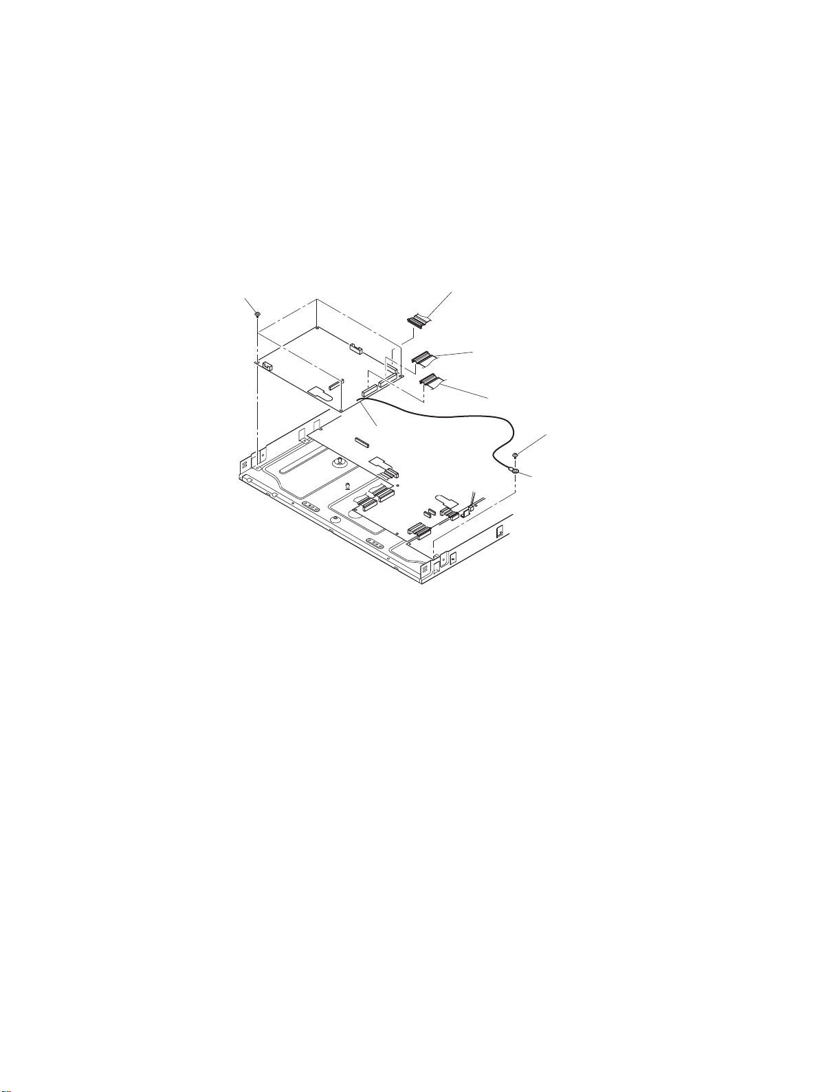
1-2-2. Mother PC Board
(1) Remove the front panel. (Refer to item 1-1-2.)
(2) Remove the RAM drive. (Refer to item 1-1-4.)
(3) Remove the rear panel. (Refer to item 1-1-6.)
(4) Disconnect five connectors (1).
(5) Remove six screws (2), and then remove the mother PC board (3).
Screws (2)
Mother PC board (3)
Connector (1)
Connectors (1)
Connectors (1)
Fig. 2-1-8
Page 13
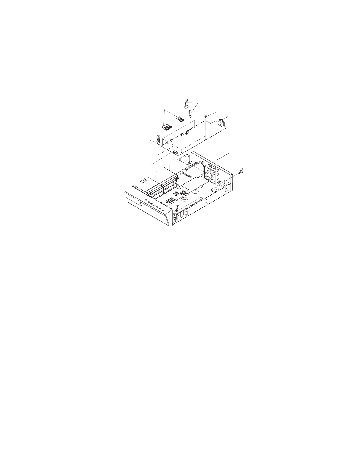
1-2-3. Power PC Board
(1) Disconnect three connectors (1).
(2) Disconnect two connectors (2).
(3) Remove the screw (3) and four screws (4).
(4) Remove the power PC board (5).
Connectors (2)
Connector (1)
Power PC board (5)
Connectors (1)
Screws (4)
Screw (3)
Fig. 2-1-9
Page 14
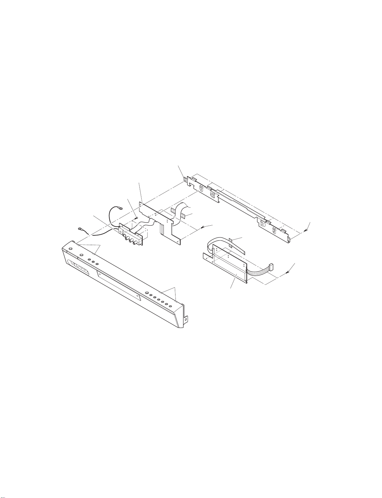
1-2-4. Front (R), Front (L) and Jack PC Board
(1) Remove the top cover. (Refer to item 1-1-1.)
(2) Remove front panel. (Refer to item 1-1-2.)
(3) Remove two pieces of tape (1).
(4) Remove six screws (2), four claws and the stay (3).
(5) Remove three screws (4) to remove the front (R) PC board (5).
(6) Remove two screws (6) to remove the front (L) PC board (7).
(7) Remove four screws (8) to remove the jack PC board (9).
(Note)
After replacing, tape on two points (1) as they were.
Stay (3)
Front (L) board (7)
Screws (8)
Jack PC board (9)
Tape (1)
Screws (2)
Screws (6)
Tape (1)
Claws
Screws (4)
Claws
Front (R) board (5)
Fig. 2-1-10
Page 15
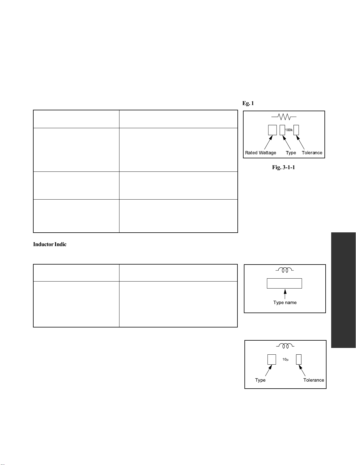
SECTION 3
100k
Rated Wattage Type Tolerance
Type name
10
m
Type Tolerance
SERVICING DIAGRAMS
1. CIRCUIT SYMBOLS AND SUPPLEMENTARY EXPLANATION
1-1. Circuit Symbols
Solid Resistor Indication
Tab. 3-1-1
Unit None ........... Ω
K ........... kΩ
M ........... MΩ
Tolerance None ...........±5%
B ........... ±0.1%
C ........... ±0.25%
D ........... ±0.5%
F ........... ±1%
G ........... ±2%
K ........... ±10%
M ........... ±20%
Rated Wattage (1) Chip Parts
None .........1/16W
(2) Other Parts
None .........1/6W
Other than above, described in the Circuit Diagram.
Type None ...........Carbon film
S ........... Solid
R ........... Oxide metal film
M ........... Metal film
W ...........Cement
FR ........... Fusible
Inductor Indication
Tab. 3-1-2
Unit None ........... Η
µ ...........µH
m ...........mH
Tolerance None ...........±5%
B ........... ±0.1%
C ........... ±0.25%
D ........... ±0.5%
F ........... ±1%
G ........... ±2%
K ........... ±10%
M ........... ±20%
Eg. 1
Fig. 3-1-1
SERVICING DIAGRAMS
Eg. 2
SECTION 3
Fig. 3-1-2
Eg. 3
Fig. 3-1-3
Page 16
100
m
Temperature
response
Rated
voltage
Tolerance
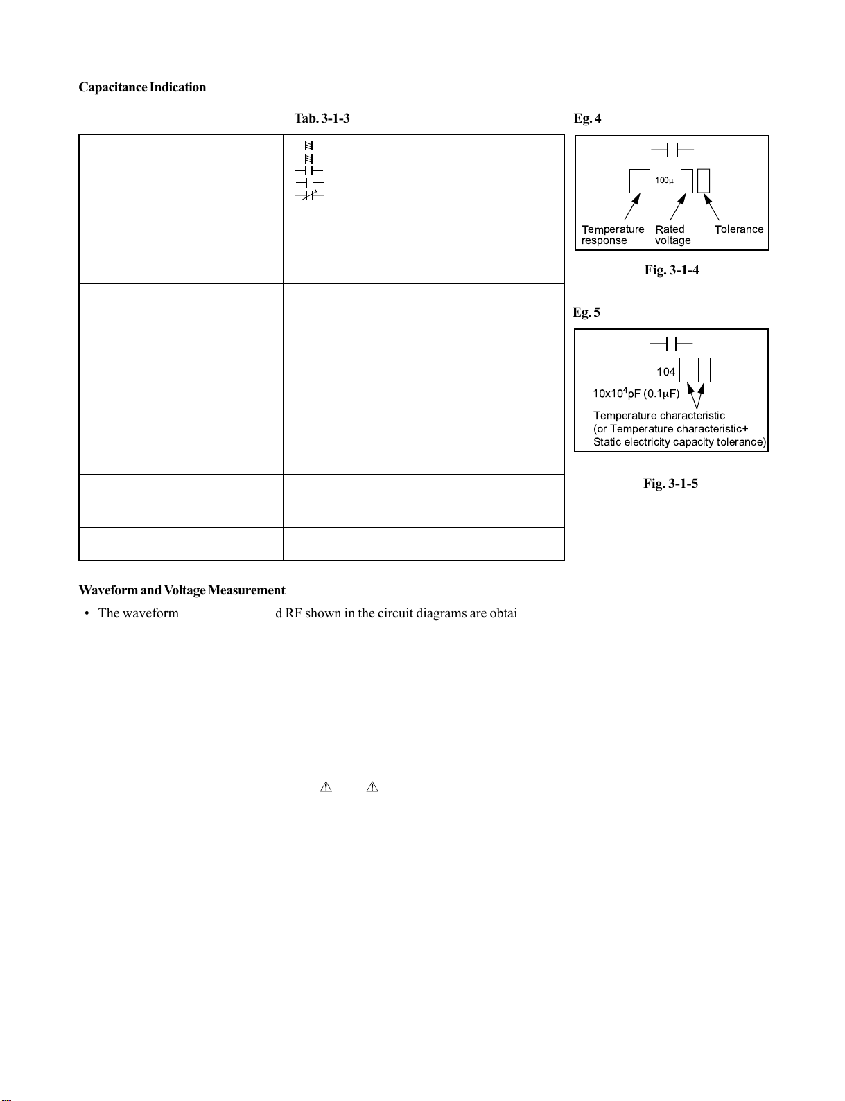
Capacitance Indication
Tab. 3-1-3
Symbol
Unit None ........... F
Rated voltage None ...........50V
Tolerance (1) Ceramic, plastic, and film capacitors of which
Temperature characteristic None ...........SL
(Ceramic capacitor) For others, temperature characteristics are
Static electricity capacity Sometimes described with abbreviated letters as
(Ceramic capacitor) shown in Eg. 3.
+
........... Electrolytic, Special electrolytic
NP
........... Non polarity electrolytic
........... Ceramic, plastic
M
........... Film
........... Trimmer
µ ...........µF
p ........... pF
For other than 50V and electrolytic capacitors,
described in the Circuit Diagram.
capacitance are more than 10 pF.
None ...........±5% or more
B ........... ±0.1%
C ........... ±0.25%
D ........... ±0.5%
F ........... ±1%
G ........... ±2%
(2) Ceramic, plastic, and film capacitors of which
capacitance are 10 pF or less.
None ...........more than ±5 pF
B ........... ±0.1 pF
C ........... ±0.25 pF
(3) Electrolytic, Trimmer
Tolerance is not described.
described. (For capacitors of 0.01 µF and
no indications are described as F.)
Eg. 4
Fig. 3-1-4
Eg. 5
104
4
pF (0.1mF)
10x10
Temperature characteristic
(or Temperature characteristic+
Static electricity capacity tolerance)
Fig. 3-1-5
Waveform and Voltage Measurement
• The waveforms for CD/DVD and RF shown in the circuit diagrams are obtained when a test disc is played back.
• All voltage values except the waveforms are expressed in DC and measured by a digital voltmeter.
Others
• The parts indicated with "NC" or "KETU" etc. are not used in the circuits of this model.
1-2. Precautions for Part Replacement
• In the schematic diagram, parts marked (ex. F801) are critical part to meet the safety regulations, so always use
the parts bearing specified part codes (SN) when replacing them.
• Using the parts other than those specified shall violate the regulations, and may cause troubles such as operation
failures, fire etc.
Page 17
2. PRINTED WIRING BOARD AND SCHEMATIC DIAGRAM
LEADS
CABLE
7
6
5
4
W002
3
2
POWER
12V (YELLOW)
CN104
123
CN10 5
GND
FL_5V
Ever+5V
Vkk
FL(-)
FL(+)
GND1
G N D ( B L ACK)
G N D ( B L ACK)
5V (RED)
4
127301119 K2
127301113K2
CN10 2
GND
D5V
GND
D3.3V
GND
D3.3V
GND
D1.5V
GND
D1.5V
GND
D1.5V
LNB ON/OFF
CPU5V
NC
PWR_ON0
PWR_ON1
FAN_CTL
PWR_GOOD
CN10 1
GND
O N / OF F +9V
GND
ON/OFF-9V
GND
EVER6V
GND
EVER6V
GND
LNB
GND
ON/OFF37V
GND
MOTOR 12V
CN10 6
1
FAN
MOTOR GND
3
LEADS
CABLE
12345
6
7 GND
EVER+ 5V
FL_5V
W002
GND
FL(+)
FL(-)
Vkk
MOUNT
FRONT LEFT
MOUNT
FRONT RIGHT
Driver_C S
CN10 1
GND 1
2345678
52806-101 0
Driver_SC K
Driver_Out
LED_Out2
Driver_I n
LED_Out1
LED_Out0
EJECT_KEY
LED_Scan2
10
9
LED_Scan1
PowerLE D
CN11 6
2827262524
LED_Scan0
LED_OUT3
LED_OUT1
LED_OUT0
LED_OUT2
232221
W053
FFC
10
987654321 Eject_Key
Driver_SC K
Driver_C S
CN70 4
GND
19
18
17
16
15
14
13
12
11
10
B-B
9
8
7
6
5
4
3
2
1
1
2
3
4
5
6
7
B-B
8
9
10
11
12
13
CN70 0
19
GND
18
D5V
17
GND
16
D3.3V
15
GND
14
D3.3V
13
GND
12
D1.5V
11
GND
10
D1.5V
9
GND
8
D1.5V
7
LNB ON/OFF
6
CPU5V
5
PWR_ON2
4
PWR_ON0
3
PWR_ON1
2
FAN_SEL
1
CYC_HA L
CN70 1
1
GND
2
ON/OFF+9V
3
GND
4
ON/OFF-9V
5
GND
6
EVER6V
7
GND
8
EVER6V
9
GND
10
LNB15.3V
11
GND
1213ON/OFF37V
GND
TWG-P13P-
TWG-P19P-A1
TWG-P23P-A1
CR-OUT
CNW01
GND
GND
23222120191817161514131211
23222120191817161514131211
CR-OUT
CNZ01
GND
GND
12730112
A1
52559-4082
B_DRESET
D_GND
CN50 6
B_DD7
123456789
123456789
RESETX
DATA7
GND
CB-OUT
CB-OUT
3K2
B_DD8
DATA8
LED_Scan2
LED_Out1
LED_Out0
LED_Out2
Driver_Out
Driver_I n
52806-101 0
CN70 8
MOTHER
CV-OUT
B-B
V-OUT
GND
GND
C-OUT
C-OUT
PB+LCH
PB-LCH
GND
10
987654321
10
987654321
PB+LCH
PB-LCH
GND
GND
GND
CY-OUT
Y-OUT
GND
GND
CY-OUT
Y-OUT
GND
GND
DIGITAL
B_DD10
B_DD11
B_DD12
B_DD6
DATA6
B_DD9
DATA9
B_DD5
DATA5
DATA10
B_DD13
B_DD4
B_DD3
B_DD2
B_DD1
10111213141516171819202122232425262728
W051
10111213141516171819202122232425262728293031323334353637383940
DATA11
DATA12
DATA13
DATA4
DATA3
DATA2
DATA1
12345
LED_Scan1
LED_Scan0
PowerLE D
EVER6V
GND
GND
EVER6V
GND
GND
B_DD14
B_DD15
B_DD0
DATA14
DATA15
DATA0
678
LED_OUT1
LED_OUT3
LED_OUT2
PB+RCH
PB-RCH
GND
PB+RCH
PB-RCH
GND
B_DMARQ
D_GND
NC
DMARQ
GND
RSV
LED_OUT0
MUTE
MUTE(DAC)
D_GND
FFC
GND
52807-281 0
LineAutoKe y
Rimcon out
PowerKey
RimEna
GND
Key2
191817161514131211
20
W052
101112131415161718
9
LineAutoKe y
PowerKey
RimEna
Rimcon
GND
Key2
52806-2810
IEC958
IEC958
B_IORDY
B_DI OW
B_DIOR
D_GND
NC
NC
SPSYNC
DIOWX
DIORX
IORDY
GND
GND
Key_Enable
Key1
Buzzer
Audio_R
Audio_L
GND
GND
GND
10
987654321
Video_COMP
GND
FFC
19
202122232425262728
Video_CONP
Audio_R
Audio_L
KeyEna
Buzzer
Key1
GND
GND
GND
GND
TWG-P19P-
A1 TWG-P13P-A1
RXD(E-T)
TXD(T-E)
RTS(T-E)
CTS(E-T)
CN70 2
CN50 7
B_DMACK
D_GND
2930313233343536373839
DMACKX
GND
E_RESET
TXD(T-R)
RTS(T-R)
CTS(R-T)
9K2
B_DA1NCB_DA0
PDIAGX
DA1
DA0
D1.5V
GND
SH_RESET
D1.5V
GND
B_CS2
B_CS0
B_CS1
CS0X
CS1X
DA2
GND
191817161514131211
191817161514131211
RXD(R-T)
GND
12730111
B_INTRQ
NC
IOCS16X
INT RQ
Video_C
Video_ Y
Line2_ S
GND
GND
Video_C
Video_ Y
Line2_ S
GND
GND
D1.5V
D1.5V
D3.3V
GND
GND
GND
GND
10
987654321
B-BB-B
10
987654321
D1.5V
D1.5V
D3.3V
GND
GND
GND
GND
D_GND
TP874
40
DASPX
GND
Video_COMP
D3.3V
GND
D3.3V
GND
Line2_ S
GND
Video_ C
GND
Video_ Y
GND
GND
Audio_L
GND
Audio_R
D5V
D5V
GND
GND
CN50 5
11
10
9
8
P AR A L LEL
7
6
5
4
W003
3
2
1
52559-408 2
A_DRESET
D_GND
123456789
A_DD10
A_DD7
A_DD8
A_DD6
A_DD9
A_DD5
11
Line2_ S
10
GND
9
Video_ C
8
GND
7
Video_ Y
6
GND
Video_COMP
5
4
GND
3
Audio_L
2
GND
1
Audio_R
W012
10
987654321 5vcpu
CN70 3
EE40
GND
TxD-RxD
52806-101 0
CV/Y-IN
GND 13
CN90 2 CN40 1
121110
131211
CV/Y-IN
GND
127301113 K2
A_DD11
A_DD12
A_DD13
A_DD4
A_DD3
A_DD2
A_DD1
101112131415161718
A_DD14
-
GND
GND
GND
C-IN
10
C-IN
A_DD0
12345
CN11 5
TPBop
TPBon
TPAon
TPAop
GND
MOUNT
S5B-PH-K-S(LF)
JACK
TimerReset
WriteEnable
A_IORDY
NC
B8B-PH-K-S
CN70 6
TPO+
TPO-
GND
GND
1234567
A_DINT RQ
A_DMACK
D_GND
A_DA1NCA_DA0
NC
GND
TPI+
TPI-
no use
A_CS2
REC_LRC K
REC_DATA
REC_ACK
REC_BCK
RESET1X
GND
GND
GND
GND
987654321
987654321
REC_LRC K
REC_DATA
REC_ACK
REC_BCK
RESET1X
GND
GND
GND
GND
A_DMARQ
A_DD15
D_GND
192021222324252627282930313233343536373839
A_DIOR
A_DI OW
D_GND
D_GND
D_GND
NC
GND
8
A_CS0
A_CS1
TP824
D_GND
40
1234567
FLSSHW -X
CN50 1
D3.3V
CTS2
RTS2
B8B-PH-SM3-TB(L
8
TXD2
RXD2
GND
GND
F) B5B-PH-SM3-TB(LF)
12345
CN50 0
TpAop
DGND
1394 SHIELD
LEADS CABLE
W004
TpBon
TpBop
TpAon
W008
LEADS
CAB
LE
12V (YELLOW)
123
GND (BLACK)
GND (BLACK)
5V (RED)
4
W051A
DRESETB
D_GND
B_DD7
B_DD8
B_DD6
123456789
RAM DRIVE
123456789
RESETX
DATA7
DATA8
DATA6
GND
ATAPI-FFC-UNT
B_DD10
B_DD11
B_DD12
B_DD9
DATA9
B_DD5
DATA5
DATA10
B_DD13
B_DD4
B_DD3
B_DD2
B_DD1
10111213141516171819202122232425262728
10111213141516171819202122232425262728293031323334353637383940
DATA11
DATA12
DATA13
DATA4
DATA3
DATA2
DATA1
B_DD14
B_DD0
DATA14
DATA0
B_DD15
D_GND
DATA15
GND
NC
RSV
B_DMARQ
D_GND
DMARQ
GND
BDI OW
DIOWX
NC
GND
B_DIOR
D_GND
DIORX
GND
B_IORDY
IORDY
NC
SPSYNC
B_DMACK
B_DINT RQ
D_GND
2930313233343536373839
DMACKX
INT RQ
GND
B_DA1NCB_DA0
NC
IOCS16X
DA1
B_DASP
D_GND
B_DA2
B_CS0
B_CS1
40
PDIAGX
DASPX
CS0X
CS1X
GND
DA0
DA2
memo
W 0 0 2 L E A D S C A B LE 0 7 140 PM0011274010
W003 LEADS CABLE 11 020 PM0012278010
W 0 0 4 L E A D S C A B LE 0 5 120 PM0011275010
W 0 0 8 L E A D S C A B LE 0 4 250 PM0011273010
W012 WIREAWG22M3L160 01 160
PM0008755010
memo
W051 FFC 40 360 PM0011276010
W052 FFC 28 320 PM0011277010
W053 FFC 10 220
PM0012301010
Fig. 3-2-1
Page 18
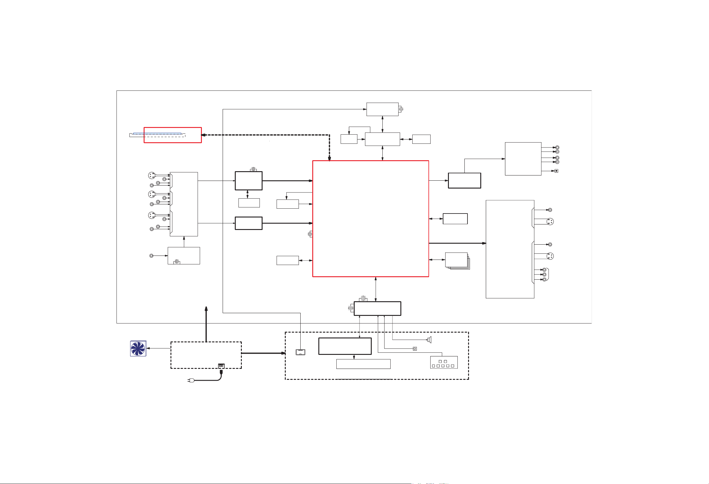
3. BLOCK DIAGRAMS
3-1. Overall Block Diagram
uPD72852
1394 PHY
IC504
24.576MHz
S-in
C_Video-in
Audio-in L/R
S-in
C_Video-in
Audio-in L/R
S-in
C_Video-in
Audio-in L/R
VHF/UHF
Type: SD-W3002
DVD RAM/RW Drive
IN_1
IN_2
INPUT
Line Selector
IN_3
V/U Tuner
ENG36501G
4.0MHz
MB01
IC301
uPD64011A
3D Y/C_DNR+
ADC+Decoder
IC302
16Mbit
SDRAM
ICA01
Audio
AD Converter
AK5365
24.576MHz
PLL
12.288MHz
27MHz
64kbit
EEPROM
PLL
12.288MHz
FRAME SYNC
ENCODE
ENCRIPT
ATAPI DRV
DECRIPT
DECODE
GRAPIC
NTSC ENCODE
MAIN CPU
32.768KHz
12.5MHz
uPD72893
1394 AV LINK
uPD6117X
Timer CPU
uPD784225Y
IC502
IC700
IC503
16Mbit
SDRAM
IC512
Audio
D/A Converter
PCM1742KE
64Mbit
FLASH ROM
256Mbit
SDRAM
X4
IC515, IC516
IC520, IC521
IC402
Audio LPF
&Amplifier
ANALOG
CIRCUIT
Audio OUT
VIDEO
ANALOG
CIRCUIT
Video OUT
OUT_1
OUT_2
OUT_1
OUT_2
INTERLACE/PROGRESSIVE/
COLOR DIFFERENCE
Video OUT
COMPOSITE
Video OUT
S Video
COMPOSITE
Video OUT
S Video
Y
Cb
Cr
Lch
Rch
Lch
Rch
OPTICAL.
DIGITAL.OUT
OUT
OUT
DC FAN
POWER_UNIT
AC IN
MPN5213
AC 120V
DV
IC101
FL_Driver
BU2879AK
FL_Tube
FRONT PANEL UNIT
R.S
KEY
Fig. 3-3-1
Page 19

3. BLOCK DIAGRAMS
3-1. Overall Block Diagram
uPD72852
1394 PHY
IC504
24.576MHz
S-in
C_Video-in
Audio-in L/R
S-in
C_Video-in
Audio-in L/R
S-in
C_Video-in
Audio-in L/R
VHF/UHF
Type: SD-W3002
DVD RAM/RW Drive
IN_1
IN_2
INPUT
Line Selector
IN_3
V/U Tuner
ENG36501G
4.0MHz
MB01
IC301
uPD64011A
3D Y/C_DNR+
ADC+Decoder
IC302
16Mbit
SDRAM
ICA01
Audio
AD Converter
AK5365
24.576MHz
PLL
12.288MHz
27MHz
64kbit
EEPROM
PLL
12.288MHz
FRAME SYNC
ENCODE
ENCRIPT
ATAPI DRV
DECRIPT
DECODE
GRAPIC
NTSC ENCODE
MAIN CPU
32.768KHz
12.5MHz
uPD72893
1394 AV LINK
uPD6117X
Timer CPU
uPD784225Y
IC502
IC700
IC503
16Mbit
SDRAM
IC512
Audio
D/A Converter
PCM1742KE
64Mbit
FLASH ROM
256Mbit
SDRAM
X4
IC515, IC516
IC520, IC521
IC402
Audio LPF
&Amplifier
ANALOG
CIRCUIT
Audio OUT
VIDEO
ANALOG
CIRCUIT
Video OUT
OUT_1
OUT_2
OUT_1
OUT_2
INTERLACE/PROGRESSIVE/
COLOR DIFFERENCE
Video OUT
COMPOSITE
Video OUT
S Video
COMPOSITE
Video OUT
S Video
Y
Cb
Cr
Lch
Rch
Lch
Rch
OPTICAL.
DIGITAL.OUT
OUT
OUT
DC FAN
POWER_UNIT
AC IN
MPN5213
AC 120V
DV
IC101
FL_Driver
BU2879AK
FL_Tube
FRONT PANEL UNIT
R.S
KEY
Fig. 3-3-1
Page 20

2 5 6 7 89
4. CIRCUIT DIAGRAMS
10134
A
B
C
4-1. Power Supply Circuit Diagram
D
E
F
G
Fig. 3-4-1
Page 21

A
B
C
134
4-2. Front Circuit Diagram
4-2-1. Front (Jack) Circuit Diagram
2 5
D
E
F
Fig. 3-4-2
G
Page 22

A
B
C
2 5 6 7 89
4-2-2. Front (L) Circuit Diagram
10134
D
E
F
G
Fig. 3-4-3
Page 23

A
B
C
2 5 6 7 89
4-2-3. Front (R) Circuit Diagram
10134
D
E
F
G
Fig. 3-4-4
Page 24

4-3. Digital Circuit Diagram
4-3-1. Digiral 1 Circuit Diagram
Fig. 3-4-5
Page 25

4-3. Digital Circuit Diagram
4-3-1. Digiral 1 Circuit Diagram
Page 26

Page 27

Page 28

Page 29

Page 30

Page 31

Page 32

Page 33

Fig. 3-4-5
Page 34

A
B
C
2 5 6 7 89
4-3-2. Digital 2 Circuit Diagram
10134
D
E
F
G
Fig. 3-4-6
Page 35

A
B
C
2 5 6 7 89
4-4. Mother Circuit Diagram
4-4-1. Tuner Circuit Diagram
10134
D
E
F
G
Fig. 3-4-7
Page 36

A
B
C
4-4-2. Timer Circuit Diagarm
2 5 6 7 89
10134
D
E
F
G
Fig. 3-4-8
Page 37

A
B
C
4-4-3. Audio Circuit Diagram
2 5 6 7 89
10134
D
E
F
G
Fig. 3-4-9
Page 38

4-4-4. Video Circuit Diagram
Fig. 3-4-10
Page 39

4-4-4. Video Circuit Diagram
Page 40

Page 41

Page 42

Page 43

Page 44

Fig. 3-4-10
Page 45

A
B
C
134
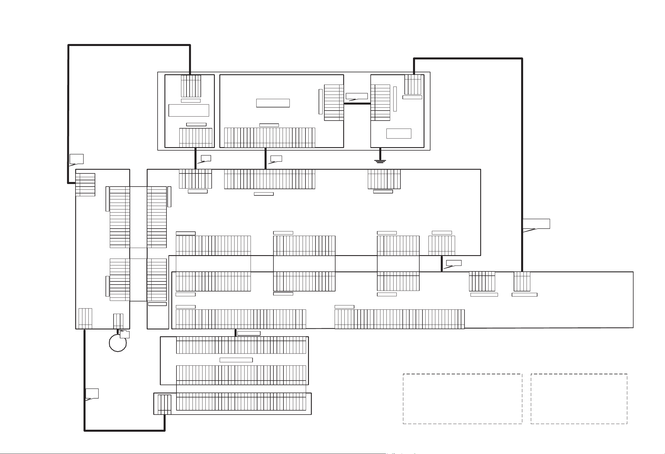
5. PC BOARDS
5-1. Front (L) PC Board
2 5
D
E
F
Fig. 3-5-1 EU03B Front (L) PC Board (Top side)
Fig. 3-5-2 EU03B Front (L) PC Board (Bottom side)
G
Page 46

A
B
C
134
5-2. Front (R) PC Board
2 5
D
E
F
Fig. 3-5-3 EU03A Front (R) PC Board (Top side)
Fig. 3-5-4 EU03A Front (R) PC Board (Bottom side)
G
Page 47

A
B
C
134
5-3. Front (Jack) PC Board
2 5
Fig. 3-5-5 EU55 Front (Jack) PC Board (Top side)
D
E
F
Fig. 3-5-6 EU55 Front (Jack) PC Board (Bottom side)
G
Page 48

5-4. Digital PC Board
C202
C203
C204C205
C206
C207
C208
C209C210
C213
C214
C215
C216
C217
C218
C301
C302
C303
C305C306
C307
C308
C309
C311C312
C313
C314
C315
C317C318
C319
C320
C321
C322
C323
C324
C325
C326
C327
C328
C329
C330
C331
C333
C335
C337
C338
C339
C340
C341
C342
C348
C349
C350
C353
C354C355
C356
C357
C358
C361
C362
C364
C365
C367
C368
C369
C370
C371C372
C373
C374C375C376C377
C380
C381
C382
C383C384
C385
C387
C388 C389
C390
C391
C392
C393
C396
C403
C406
C505
C507
C508
C511
C512
C515
C516
C519
C520
C523
C524
C527
C532
C533
C534
C535
C536
C539
C540
C541
C542
C544
C545
C546
C547
C548
C549
C550
C551
C552
C553
C554
C556
C557
C558
C565
C567
C568
C569
C574
C578
C579
C581
C586
C590
C592
C593
C594
C603
C604
C612
C613
C614
C615
C616
C617
C618
C619
C620
C621
C622C623
C624
C625
C626
C627
C628
C629
C630
C631
C632
C633
C634
C635
C636
C637
C638
C639
C640
C641
C642
C643
C644
C646
C647
C649
C650
C651C652
C653
C658
C660
C663
C664
C665
C666
C667
C668
C669
C670
C671
C672
C673
C674
CZ02
D401
D402
E301
E302
E303
E304
E305
E306
E307
E308
E310
E311
E312
E313
E315
E317
E318
E319E320
E321
E322
E324
E325
E326
E327
E328
E329
E330E331E332
E333
E334
E335
E341
E342
E343
E344
E404
E405
E406
E407
E408E409E410E411E412
E413
E414
EZ01EZ02EZ03EZ04EZ05EZ06
EZ07
EZ08
EZ09
EZ10
EZ11
EZ12
EZ13
EZ14
EZ15
EZ16
EZ17
EZ18
EZ33
EZ36
EZ37EZ38
EZ43
EZ44
EZ45
EZ46 EZ47
EZ48
EZ49
EZ50
EZ51
EZ52
EZ65
EZ66
EZ67
EZ68
EZ69
EZ70
EZ71
EZ72
EZ73
EZ74
EZ75
EZ76
EZ77
EZ78
EZ79
EZ80
EZ81
EZ82
EZ83
EZ84
EZ85
EZ86
EZ87
IC302
IC502
IC516 IC521
IC528
IC532
L302
L312
L500
L504
L505
L506
L507
L508
L510
L511
L512 L513
Q301
Q302
R201
R202
R205R206
R209
R210
R211
R212
R213
R214
R301
R302
R303R304
R305
R306
R307
R308
R309
R310
R311
R312
R313
R314
R315
R316
R317
R318
R319
R320
R321
R322
R324
R325
R326
R327
R336
R337
R338
R339 R340
R342
R343
R344
R345
R347
R348
R349
R350
R351
R352
R353
R354
R355
R356
R357
R358 R359
R360 R361
R362
R363
R364
R365
R366
R367
R368
R374
R375
R376
R377
R378
R379
R380
R381
R382
R383
R384
R385
R386 R387
R388
R389
R390
R391
R394
R395
R396
R403
R404
R405
R407
R500
R501
R503
R504
R505
R506
R507
R508
R509
R510
R511
R512
R515
R518
R521
R522
R523
R524
R528
R539
R541
R543
R545
R546
R547
R549
R551
R552
R553
R554
R556
R557
R559
R560
R563
R564
R565
R566
R567
R568
R569
R571
R572
R574
R588
R602
R604 R605R606 R609R610
R611
R612
R615
R618
R621
R623
R624
R625
R626
R627
R628R629R630 R631
R633
R634
R635
R636
R639
R640
R643
R651
R656
R662
R663
R674
R675
R676
R699R700R701R703 R704R705
R724
R725
R726
R727
R739
R740
R741
R743
R749
R751
R752
R753
R754
R755
R759
R760
R761
R762
R763
R764
R765
R766
R767
R768
R769
R770
R771
R772
R777
RM500RM501RM502RM503 RM504RM505RM506RM507
RM508RM509
RM511
RM512RM513RM514RM515
RM516
RM517RM518 RM519RM520
RM521RM522RM523RM524 RM525RM526
RM538 RM539RM541RM542 RM545RM546 RM557
RM565RM566 RM567
RM569RM570
RM571
RM576 RM577
RM578 RM579
RM580 RM581
RM582 RM583
RZ01
RZ02
RZ03
RZ04
RZ05
RZ06
RZ07
RZ08
RZ09
RZ10
RZ11
RZ12
RZ13
RZ14
RZ15
RZ16
RZ17
RZ18
RZ48
RZ52
RZ53
RZ54
RZ55
RZ56
RZ57
1234
A
B
C
D
1234
R758
FL501
C394
R714
R722
C675
R576
R577
R590
R591
R689
IC523
R711
IC527
C598 C602
D302D303
R690
FL500
C606
D301
IC303
R392
R393
IC304IC305
R715
R716
R717
R718
R723
IC535 IC536
R775
R581
R582
R583
R584
R585
R595
R596
R597
R598
R599
R691
X501
C506
IC503
C518
C525
R757
R756
C607
R719
R776
R720
C595
IC508
R519
RZ19 RZ20 RZ21 RZ22 RZ23 RZ24
C397
QZ01 QZ02 QZ03 QZ04 QZ05 QZ06
C517
C531
IC537
C661
IC518
IC522
R570
RM510
RM568
C522
R736
IC533 IC534
C662
C526
IC501
C521
RM551
RM549RM550
IC510
C555
R525
CN506
R728
R729
R773
IC524
R520
R737
IC529
C645
R778
R730
R774
R731
R738
C676
C514
R732
IC538
C510C513
R502
R733
R734
C500
CZ01
RM553RM554 RM555RM556
R735
C509
R401
R402
C402
IC401
E401E402
LZ01
C529
C409
E403
C401
R406
IC500
C502
C408
IC204
C212
X500
C404
IC402
EZ41EZ42
IC511
X201
IC504
C405
S500
IC519
IC517
IC202 IC203
R203
R204
C211
C501
L502
C503
R514
R513
R516
R517
C528
C538
C407
R207 R208
L501
C504
D201
C201
D202
CN201
L201
CN500
Fig. 3-5-8 EU01 Digital PC Board (Bottom side)
CN507CNZ01
R744
R745
R746
R747
R748
C386
RM302 RM303RM304
X301
C359 C360
Q303
L308
L311
C363C366
R632
R613
IC512
C543
R637
R638
C563
C332
RM308 RM309
L310
C564
IC515
C566
IC507
RM558RM559RM560
C573
C577
Q304
L313
R600
C571
C659
IC301
R586
R587
C570
C576
VR500
R346
L306
L309
R601
RM536
RM534
RM532
RM527RM528RM529RM530
C648
IC505
R649
R641
C572
C575
C334
E309
RM572
RM535
RM533
RM531
IC506
RM573
Fig. 3-5-7 EU01 Digital PC Board (Top side)
E316
FL302
C336
E314
FL301
CN401
A
C395
C352
C611
C655
R323 R328
C343
C351
D304
IC306
IC531
E323
R334
R329
C344 C345 C346 C347
C398
C654
R335
R333
R332
R331
R330
RM301
RM306RM307
RM305
C378
C379
B
C
D
CN503
R608
R619
CN501
R654
R655
R660
R672
R642
R670
R644
R678
C559
R589
R603
R607
R616
R617
R620
R652
R653
R661
RM575
RM561RM562RM563RM564
R687
R686
RM537RM540 RM543RM544RM547RM548
IC520
C580
IC513
R614
C583
C589
C582
C585C587
R622
C560
C562
L307
C584
C588
EZ40
C561
IC514
RM574
IC530
IC509
R712
R558
L301
R369
E336
FL503
R370
R371
E338
E337
RM552
C608
C657
FL502
R372
R373
E340
E339
CN505
C656
C609
C605
C304
R580
R594
C537
R721
R579
R593
C591
C310C316
R713
R578
R592
C530
Page 49

5-5. Mother PC Board
12345678
JW01JX01
CB54
JP014
CB53
JP028
CB21
LB09
DB05
JP018
JP022
JP160
JP060
LB10
JP020
MB02
JP013
CX03
JP081
JP026
CX15
CX19
CX23
CX25
JP029
CX01
R730
CX07
CX12
JP031
CX21
JP023
JP220
JP171
JP042
JP059
JP039
JP104
R711
JP032
JP071
JP053
CX18
CX26
JP033
CN708
R712
JP030
CX24
JP040
CX20
CX05
JP041
JP025
JP044
JP027
JP035
JP051
JP036
JP079
JP043
JP285
JP054
JP034
JP061
JP055
JP056
JP049
CX28
JP072
CX06
CX09
JP259
JP257
JP260
JP078
JP058
JP157
JP046
CX11
JP052
JP050
JP062
JP261
JP047
JP069
JP048
JP074
JP092
JP070
JP258
CX57
JP237
CX33
JP063
CX35
JP064
JP073
FLX02
CX51
JP067
FLX01
JP065
CX40
C967
C963
JP077
JPX04
C965
C974
JP309
CX54
CNW02
JP068
JPX03
C961
JP263
JP264
JP082
JP262
CX38
JPX01
CX53
JP098
LX02
JP076
JP236
C964
JP075
CX48
C973
JP099
CN902
JP088
JP265
RA47
JP086
C966
RA04
JP085
JP124
RA12
JP083
JP125
JP255
RA55
JP100
C962
JPA05
JP301
C959
C957
JPA02
JPA03
C922
JP102
CA92
C947
JP121
JP120
JP080
C955
JP087
JP101
C953
JP238
JP096
JP219
JP093
JP266
JP267
JP158
JP234
CNW01
C954
C929
JP084
JP166
JP163
JP159
JP135
JP123
JP268
R725
R761
JP169
JP122
R726
R727
JP235
C906
C907
C933
JP244
JP066
JP127
JP224
JP164
R759
R760
R758
JP304
JP162
JP165
JP181
JP269
CA98
JP239
JP132
R710
JP152
C908
C909
JP253
R770
JP149
CA99
CA94
CB84
RB20
JP005
JP003
CB81
JP002
RB92
MB01
JP001
CB86
JP015
CB01
JP024
CB06
JP090
RB55
CB15
JP242
JPB02
CB12
CB60
RB27
CNB02
QB05
CB08
JPB01
KB01
RB08
CB04
JP010
CB39
JP019
CB14
JP038
JP012
JP011
JP008
CB69
CB18
JP009
CB61
CB03
CB62
JP045
DB02
CB45
DB01
JP016
LB01
JP057
JP021
LB11
LB05
LB08
CB68
CB46
DB07
LB07
CB52
JP017
CB65
CB67
A
CB11
JP006
RB21
LB04
CB17
B
DB06
CB10
JP004
JP007
JP037
CB83
C
D
RB91
E
F
CN702
JP089
JP105
C727
C725
C932
R749
JP153
C905
JP116
JP114
R704
JP115
R757
JP129
JP256
R718
JP156
JP302
JP203
JP091
R762
C726
JP184
JP185
JP119
JP182
JP180
JP178
JP179
JP113
JP112
JP146
JP095
ICA24J901 J902
JP243
C918
JP128
JP103
JP138
JP245
JP170
JP131
JPA04
JP168
CW17
CW18
JPX05
JP272
JP271
JP273
JP274
JP303
JP155
JP117
JP151
JP286
JP270
R773
JP252
JP110
R769
JP108
JP134
JP133
JP172
JP109
JP136
L702
L703
C951
JP130
CW14
JP275
JP287
JP198
R772
R707
CW15
CW08
JP276
JP288
JP294
JP202
JP241
JP161
JP277
JP289
JP295
JP137
R708
R754
JP240
X700
R753
R752
CW16
CW07
JP278
JP290
JP291
JP296
JP279
JP297
JP190
CW13
JP187
JP280
JP292
JP196
JP249
JPA01
RA17
CW06
JP306
JP281
JP293
JP228
R717
R750
JP186
JP307
JP207
R748
JP188
JP305
JP282
JP118
R763
JP144
R747
CW25
R714
R719
CN707
CW11
R713
JP300
JP298
JP143
R785
R746
CN706
JP299
JP195
R721
R745
JP189
JP211
JP209
RW05
RW09
JP148
JP177
R784
R722
R744
JP167
R723
R743
JP213
JP210
R728
R742
JP246
CW09
CW01
JP283
R700
JP142
JP094
JP214
RW08
RW07
RW06
RW12
RW10
RW11
JP204
JP150
JP147
R724
R741
JP215
JP212
JP284
JP145
R729
JP107
R764
JP173
C702
JP205
R755
R756
JP176
JP227
JP206
JP154
JP111
JP174
JP201
R740
JP192
JP183
JP199
R731
R732
R734
R735
R736
JP140
JP193
JP223
RT700
JP175
JP106
JP139
JP200
JP194
CX44
LX03
JP222
R720
JP208
JPX02
JP097
JP126
RX76
JP218
JP141
JP226
C993
JP191
JP232
R786
R768
C971
R938
C752
R767
R939
RX75
CN703
CN704
C910
C949
C972
C750
JP254
CX43
C754
JP308
JP197
C994
JP250
JP233
JP247
JP251
JP230
JP229
JP231
CN700 CN701
JP225
JP248
JP221
R787
JP216
Fig. 3-5-9 EU05 Mother PC Board (Top side)
Page 50

12345678
RA08
RX01
RX06
RA36
RX03
RA19
RX02
CX02
RA23
RB54
RB59RB60
CB51
RB63
CB49
CB48
RB36
RB62
RB18
RB22
CB23
RB17
CB63
CB64
RB26
RB23
CB24
CB36
RB01
CB35
RB29
CB09
RB40
ICB01
RB44
RB03
RB32
RB02
RB49
RB41
RB11
CB02
RB38
QB07
RB42
RB51
CB71
RB46RB47
CB70
RB39
QB06
RB30
CB40
RB43
RB28
DB08
CB05
QB08
QB10
CB22
CB20
RB14
RB19
CB16
CB25
RB71
RB72
CB26
RB24
RB25
RB09
CB13
RB61
CB88
QB84
ICB81
RB15
RB16
RB06
RB45
RB81
RB82
CB80
RB85
RB90
RB89
RB07
CB82
RB86
QB82
RB83
ICB80
RB84
RB80
QB83
RB87RB88
CB85 CB87
RX39
RX38
RX18
RX10
ICX05
DX04
DX06
CX10
QX02
CX27
RX20
CX08
ICX02
RX57
R733
RX24
RX58
RX59
QX01
CX04
RX23
RX64
RX04
ICX01
RX63
RX14
RX67
RX17
RX15
RA61
QX10
RX79
RX45
RX86
RA59
CX32
RX44
QX03
RX40
CX31
ICX06
CX29
RX25
RX43
DX07
RX29
RX42
CX30
Q901
DW08
D903
QA04
RW27
RW32
RW35
RW37
RW36
RW34
RW30
R911
R946
DW14
R947
R919
R915
CA01
RA95
RW21
CW05
DW04
C917
RW40
ICA21
R953
RA97
DW07
RW26
C950
C915
DW12
RW31
A
RW17
CW02
DW01DW02
RW16
RW38
CW04
CW03
DW06
RW25
ICW01
RW39
D901
R926
R927
R975
DW03
DW05
C989
ICA32
C984
RW18
B
DA10
DA11
DA12
DA13
R937
C928
C944
ICX10
CX42
R936
CX46
CX45
R930
D902
R929
CW26
R976
CW19
QW03QW04
RW22
CW21
R983
R900
LA20
QA03
DW09
DW10 DW11
RW28
RW04
QW02
CA51
DA09
R931
RW29
QW01
RW01
Q902
C
C701
IC701
R702
C751
C703
L701
R701
R703
C700
R925
RA31
DW13
CW23
CW24
R943
R912
RW33
R940 R941
R907
R908
RA92
L902
C952
R923
R916R917
C934
ICA07
R998
RA81
R922
RA46
RA39
QA01QA02
CA18
R921
R909
Q910Q911
RA79
R965
R952
C948
RA78
R967
C956C958
R957
R968
R974
R966
RW19
R969
CW20
R990
R960
R964
L903
C902
C904
RW20
ICA01
R942
RA82
RW23
CW22
RW24
RA25
C901
R992
IC910
R981
RX78
IC909
R901
CX47
R902
RX77
R993
ICX09
R987
RA28
C921
RA27
QX04
C945
C946
LA03
RA52
RA14
RA02
CX49
CX50
RX53
R986
R991
R988
R979
CX37
RX52
CX41
RA03
RA60
RA44
RX48
RX50
RX51
RX85
QX05
CX39
RX49
RX69
CX52
QX08
QX11
CX55
RX92
RX81
R737
RA21
RX54
ICX07ICX08
CX34
R715
RX90
RX88
RX82 RX83
RA51
RA43
RX56
CX56
RX89
RX84
RX98
QX06
R738
RX47
RX91
RX99RY01
QX09
RX80
R771
RX46
RX55
RX87
RY02
QX07
R739
RX33
CX17
DX09
RX08
CX13
RX34
RX07
RX27
CX14
RX13
RX62
ICX04
RX32
RX09
RX60
RX66
RX26
RX31
D700
RX19
RX11
RX28
CX22
RX61
RX65
DX05
DX08
ICX03
RX41
CX16
RX05
DX01 DX02DX03
D
C757
E
F
C755
C756
C712
R774
C753
C723
C716
C714
IC700
C715
C709
R751
C708
C724
R716
C707
R709
R705
R706
X701
C706
C705
C713
C704
C710
RA34
IC702
L704
C903
RA72
RA40
RA41
ICA19
C718
RA38
R989
C721
RA73
C930
R910
C717
C719
C720
C722
Fig. 3-5-10 EU05 Mother PC Board (Bottom side)
Page 51

SECTION 4
PARTS LIST
SAFETY PRECAUTION
The parts identified by ! ( ) mark are critical for safety. Replace only with part number specified.
The mounting position of replacement is to be identical with originals.
The substitute replacement parts which do not have the same safety characteristics as specified in the parts list may create
shock, fire or other hazards.
NOTICE
The part number must be used when ordering parts in order to assist in processing, be sure to include the model number and
description.
ABBREVIATIONS
1. Integrated Circuit (IC)
2. Capacitor (Cap)
• Capacitance Tolerance (for Nominal Capacitance more than 10pF)
Table 4-2-1
Symbol
Tolerance %B± 0.1C± 0.25
Symbol
Tolerance %
• Capacitance Tolerance (for Nominal Capacitance 10pF or less)
Symbol
Tolerance pFB± 0.1C± 0.25
3. Resistor (Res)
• Resistance tolerance
Symbol
Tolerance %B± 0.1C± 0.25
P
+ 100
0
Q
+ 30
– 10
D
± 0.5
T
+ 50
– 10
D
± 0.5
Ex. 10pF G = 10pF ± 2pF
D
± 0.5
F
± 1
U
+ 75
– 10
Table 4-2-2
F
± 1
Table 4-3-1
F
± 1
± 2
+ 20
– 10
± 2
± 2
G
V
G
G
J
± 5
W
+ 100
– 10
J
± 5
K
± 10
X
+ 40
– 20
Ex. 10µF J = 10µF ± 5%
K
± 10
M
± 20
Y
+ 150
– 10
M
± 20
N
± 30
Z
+ 80
– 20
PARTS LIST
SECTION 4
Ex. 470ΩJ = 470Ω± 5%
Page 52

4. EXPLODED VIEWS
4-1. Packing Assembly
ZF10
ZF11
ZF23
ZF01
Note: The shape of the packing
material is sometimes different.
Fig. 4-4-1
Page 53

4-2. Chassis Assembly
ZG20
W051
W051A
RAM1
EU05
W052
W053
EU01
EU03B
ZG45
EU02
EU55
EU03A
ZG01
Fig. 4-4-2
Page 54

5. PARTS LIST
LOCATION
NUMBER
- MECHANICAL PARTS -
! RAM1 P000391340 DVD-RAM SD-W3002-TC
W051 P000387340 Cable,Flexible FFC,40P,L360
W051A P000391300 CONV Unit,ATAPI-FFC
W052 P000387350 Cable,Flexible FFC,28P,L320
W053 P000387360 Cable,Flexible FFC,10P,L220
ZF01 P000387370 Remote Control UnitSE-0105
! ZF10 P000376390 Owners Manual,OP English
! ZF10 P000376480 Owners Manual,OP French,DR1SC
! ZF11 P000376380 Owners Manual,ST English
! ZF11 P000376470 Owners Manual,ST French,DR1SC
! ZF12 P000384770 Owners Manual,Q English,DR1SU
! ZF23 79088007 Power Cord
ZG01 P000387400 Front Panel
ZG20 P000387330 Cover,Top
ZG45 P000387390 Fan,DC D06T12TS901
PART
NUMBER DESCRIPTION
Page 55

LOCATION
NUMBER
PART
NUMBER DESCRIPTION
- ELECTRICAL PARTS -
EU01 P000387260 PC Board Assy Digital,D-R1SU
EU01 P000391330 PC Board Assy Digital,D-R1SC
- INTEGRATED CIRCUITS -
IC301 P000391200 IC UPD64011AGM-8ED-Y
IC302 P000391160 IC K4S161622D-TC80000
IC303 P000377900 IC MM1563DFBE
IC304 P000377900 IC MM1563DFBE
IC305 P000391250 IC MM1561FFBE
IC306 P000377900 IC MM1563DFBE
IC401 79040379 IC NJM2870F05
IC402 79040396 IC PCM1742KE2K
IC500 P000391280 IC PQ070XZ01ZPH
IC502 P000391220 IC UPD72893AGD
IC503 79040163 IC MT48LC1M16A1TG
IC504 P000391230 IC UPD72852AGB-8EU
IC505 P000391130 IC TC7S04FU
IC506 P000391190 IC PLL1707DBQ
IC507 P000391270 IC BA7082F
IC509 P000378050 IC SN74AHC1G04HDCKR
IC510 P000378050 IC SN74AHC1G04HDCKR
IC513 P000391280 IC PQ070XZ01ZPH
IC515 P000391210 IC K4H560838D-TCB000
IC516 P000391210 IC K4H560838D-TCB000
IC517 P000378040 IC SN74AHC1G08HDCKR
IC518 P000391170 IC MBM29DL640E90TN
IC519 79040306 IC PST594JMT
IC520 P000391210 IC K4H560838D-TCB000
IC521 P000391210 IC K4H560838D-TCB000
IC523 P000378030 IC SN74LVC244APWR
IC527 P000391290 IC PQ1X331M2ZPH
IC528 P000391240 IC NJM2125F
IC529 P000378050 IC SN74AHC1G04HDCKR
IC531 P000377900 IC MM1563DFBE
- TRANSISTORS -
Q303 79050018 Transistor,Chip 2SA1162
Q304 79050018 Transistor,Chip 2SA1162
QZ01 79050018 Transistor,Chip 2SA1162
QZ02 79050018 Transistor,Chip 2SA1162
QZ03 79050018 Transistor,Chip 2SA1162
QZ04 79050018 Transistor,Chip 2SA1162
QZ05 79050018 Transistor,Chip 2SA1162
QZ06 79050018 Transistor,Chip 2SA1162
- DIODES -
D301 79060019 Diode,Chip 1SS355
D302 79060019 Diode,Chip 1SS355
D303 79060019 Diode,Chip 1SS355
D304 79060019 Diode,Chip 1SS355
D401 79060019 Diode,Chip 1SS355
D402 79060019 Diode,Chip 1SS355
- MISCELLANEOUS -
X301 79089168 Oscillator,Crystal
X500 79089168 Oscillator,Crystal
X501 P000377990 Crystal 27.0M
!
EU02 P000387380 PC Board Assy Power
EU03A P000387290 PC Board Assy Front(R),Display
- INTEGRATED CIRCUITS -
IC101 P000377960 IC BU2879AK
- TRANSISTORS -
Q101 79050089 Transistor RN2401
Q102 79050089 Transistor RN2401
Q105 P000391100 Transistor DTD143EK
- DIODES -
D101 79060022 Diode,Chip 1SS368
D102 79060022 Diode,Chip 1SS368
D118 79060077 Diode,LED SLA-360MT
D119 79060100 Diode,LED SLI-325URCT31
D126 79060022 Diode,Chip 1SS368
D127 79060022 Diode,Chip 1SS368
D128 79060022 Diode,Chip 1SS368
D129 79060022 Diode,Chip 1SS368
D134 79060022 Diode,Chip 1SS368
D135 79060022 Diode,Chip 1SS368
D136 79060022 Diode,Chip 1SS368
D137 79060022 Diode,Chip 1SS368
D138 79060022 Diode,Chip 1SS368
LOCATION
NUMBER
PART
NUMBER DESCRIPTION
D139 79060022 Diode,Chip 1SS368
D140 79060022 Diode,Chip 1SS368
- MISCELLANEOUS -
A101 P000391090 Display FL HNV-10SM28T
S102 P000391050 Switch,Tact
S111 P000391050 Switch,Tact
S112 P000391050 Switch,Tact
S113 P000391050 Switch,Tact
S114 P000391050 Switch,Tact
S115 P000391050 Switch,Tact
S116 P000391050 Switch,Tact
EU03B P000387410 PC Board Assy Front(L)
- INTEGRATED CIRCUITS -
IC102 P000391110 Module,IR GP1UM281RK
- TRANSISTORS -
Q108 79050089 Transistor RN2401
Q109 79050009 Transistor,Chip RN1401
Q110 79050089 Transistor RN2401
Q111 79050089 Transistor RN2401
Q112 79050089 Transistor RN2401
Q113 79050089 Transistor RN2401
Q114 79050089 Transistor RN2401
Q115 P000391100 Transistor DTD143EK
- DIODES -
D117 79060099 Diode,LED SLI-325DCT31
D120 79060091 Diode,LED LED, MVL-354B-T
D121 79060091 Diode,LED LED, MVL-354B-T
D122 79060091 Diode,LED LED, MVL-354B-T
D123 79060033 Diode,LED
D124 79060022 Diode,Chip 1SS368
D125 79060022 Diode,Chip 1SS368
D142 79060022 Diode,Chip 1SS368
D191 79060022 Diode,Chip 1SS368
- MISCELLANEOUS -
BZ101 P000377950 Buzzer PS1240P02AT
S101 P000391050 Switch,Tact
S103 P000377940 Switch,Push-Lever
S118 P000391050 Switch,Tact
S120 P000391050 Switch,Tact
S121 P000391050 Switch,Tact
S122 P000391050 Switch,Tact
EU05 P000387270 PC Board Assy Mother
- INTEGRATED CIRCUITS -
IC700 79040330 IC UPD78F4225YGC-8
IC701 P000391180 IC PST3222NR
IC702 P000391150 IC DC74HCT125M
IC909 P000391140 IC TC74VHC125F
IC910 P000391120 IC TC7SET04F
ICA01 P000377930 IC AK5365VQ
ICA07 79040379 IC NJM2870F05
ICA19 79040044 IC NJM4580E
ICA21 79040074 IC TC74HCU04AF
ICA24 79089024 Terminal,Optical TOTX178
ICA32 79040044 IC NJM4580E
ICB01 P000363360 IC CXA2064M
ICB80 79040371 IC BA7046F
ICB81 P000363370 IC NJM2330MV
ICW01 P000391260 IC MM1568DJBEG
ICX01 79040381 IC MM1503XNRE
ICX02 79040381 IC MM1503XNRE
ICX03 79040381 IC MM1503XNRE
ICX04 79040382 IC MM1140XFFE
ICX05 79040369 IC MM1113XFBE
ICX06 P000377890 IC MM1501XNRE
ICX09 79040379 IC NJM2870F05
ICX10 79040374 IC PQ05DZ1U
- TRANSISTORS -
Q901 79050100 Transistor,Chip RN1402
Q902 79050001 Transistor,Chip RN2402
Q910 79050100 Transistor,Chip RN1402
Q911 79050100 Transistor,Chip RN1402
QA01 79050014 Transistor,Chip HN1C03F
QA02 79050014 Transistor,Chip HN1C03F
QA03 79050100 Transistor,Chip RN1402
QA04 79050001 Transistor,Chip RN2402
QB08 79050016 Transistor,Chip 2SC2712
QB10 79040374 IC PQ05DZ1U
QB82 79050016 Transistor,Chip 2SC2712
QB83 79050100 Transistor,Chip RN1402
QB84 79050100 Transistor,Chip RN1402
Page 56

LOCATION
NUMBER
QW02 79050100 Transistor,Chip RN1402
QW03 79050018 Transistor,Chip 2SA1162
QW04 79050018 Transistor,Chip 2SA1162
QX01 79050100 Transistor,Chip RN1402
QX02 79050016 Transistor,Chip 2SC2712
QX03 79050016 Transistor,Chip 2SC2712
QX06 79050018 Transistor,Chip 2SA1162
QX08 79050016 Transistor,Chip 2SC2712
QX09 79050018 Transistor,Chip 2SA1162
QX11 79050016 Transistor,Chip 2SC2712
- DIODES -
D700 79060019 Diode,Chip 1SS355
D901 79060028 Diode,Chip 1SS226
D902 79060028 Diode,Chip 1SS226
D903 79060019 Diode,Chip 1SS355
DA09 79060019 Diode,Chip 1SS355
DA10 79060098 Diode RB521S-30TE-61
DA11 79060098 Diode RB521S-30TE-61
DA12 79060098 Diode RB521S-30TE-61
DA13 79060098 Diode RB521S-30TE-61
DB06 79060096 Diode,Zener MTZJT-7733D
DW03 79060028 Diode,Chip 1SS226
DW04 79060028 Diode,Chip 1SS226
DW05 79060028 Diode,Chip 1SS226
DW06 79060028 Diode,Chip 1SS226
DX02 79060028 Diode,Chip 1SS226
DX03 79060028 Diode,Chip 1SS226
DX05 79060028 Diode,Chip 1SS226
DX06 79060028 Diode,Chip 1SS226
DX08 79060028 Diode,Chip 1SS226
DX09 79060028 Diode,Chip 1SS226
- RESISTORS -
- MISCELLANEOUS -
J901 P000391070 Jack Board 9P
J902 P000391320 Jack Board D-Audio Out
JW01 P000391060 Jack,S
JX01 P000391080 Jack Board,S+6P
! MB01 P000363390 Tuner,V/U ENG36501G
RT700 P000377860 Thermister NTSA0XH103EE1A0
X700 P000391040 Crystal
X701 P000363400 Oscillator,Crystal
EU55 P000387280 PC Board Assy Jack
- MISCELLANEOUS -
J101 P000387310 Jack,Pin
J102 P000387320 Jack,S
J103 P000387300 Jack,DV
PART
NUMBER DESCRIPTION
LOCATION
NUMBER
PART
NUMBER DESCRIPTION
Page 57

SPECIFICATIONS
Power requirement during operation
Power requirement at standby
Power supply
Mass
External dimension
Incoming channels
Antenna input/output terminal
Demodulation input/output terminal
Signal system
Laser
Format
Image recording system
Sound recording system
VIDEO input
VIDEO output
S-VIDEO input
S-VIDEO output
COMPONENT output (Y, PB, PR)
AUDIO input
AUDIO output
DIGITAL AUDIO output BITSTREAM/PCM (Optical
terminal)
DIGITAL AUDIO output BITSTREAM/PCM (Coaxial
terminal)
DV input
Remote control
Operating conditions
Clock display
Clock accuracy
33W
2.7W or below (Eco mode: off)
0.8W or below (Eco mode: on)
120V AC, 60 Hz
4.2kg
Width 430 x Height 78 x Depth 325mm
TV : 2-69CH, CATV : 1-125CH
VHF/UHF : 75Ω, F Connector
0.67Vp-p (75Ω) Unbalanced, Pin jack
Standard NTSC Color TV system
Semiconductor laser, Wavelength : 650nm/780nm
DVD-VR format
DVD-Video format
MPEG2
Dolby digital, M1, M2, Linear PCM
1.0Vp-p (75Ω), Sync signal negative, Pin jack x 2 systems, 2 at rear, 1 in front
1.0Vp-p (75Ω), Sync signal negative, Pin jack x 2 systems, 2 at rear
(Y) 1.0Vp-p (75Ω), Sync signal negative, Mini DIN4 Pin x 3 systems
(C) 0.286Vp-p (75Ω), 2 at rear, 1 in front
(Y) 1.0Vp-p (75Ω), Sync signal negative, Mini DIN4 Pin x 2 systems
(C) 0.286Vp-p (75Ω), 2 at rear
Y output (green), 1.0Vp-p (75Ω), Sync signal negative, Pin jack x 1 system
PB, PR output (blue, red), 0.7Vp-p (75Ω), Pin jack x 1 system each
2.0V (rms), 50kΩ or below, pin jack (L, R) x 3 systems
2 at rear, 1 in front
2.0V (rms), 200Ω or above, pin jack (L, R) x 2 systems
2 at rear
Optical connector x 1 system
0.5Vp-p (75Ω), pin jack x 1 system
4-pin x 1 in front
Wireless remote control (SE-R0105)
Temperature : 41°F to 95°F (5°C to 35°C), Position: Horizontal
24 hour digital display
Quartz (monthly deviation : approximately ±30 seconds)
• The design and specifications may change without prior notice.
• The Illustrations and screens described in this manual may be exaggerated or simplified for easy recognition and may be slightly different from the actual unit.
Page 58

TOSHIBA CORPORATION
1-1, SHIBAURA 1-CHOME, MINATO-KU, TOKYO 105-8001, JAPAN
 Loading...