


NTDCTV05
TECHNICAL TRAINING MANUAL
N5SS (TG-1, C) CHASSIS
COLOR TELEVISION
CN27E90, CX32E70
CN32E90, CN35E15
CF35E50, CX35E60
CX35E70, CX35E81
CN35E90, CN35E95
PRINTED IN JAPAN Aug. 1995 So

Contents
SECTION I
OUTLINE ...................................................................... 6
1. OUTLINE OF N5SS CHASSIS (CN32E90, CN35E90) .................................................................... 7
2. PC BOARD CONFIGURATION ........................................................................................................ 7
3. MAJOR SPECIFICATIONS (NEW FUNCTIONS IN ADDITION TO THOSE OF N5SS) ........ 7
4. MODIFICATIONS ON CHASSIS ..................................................................................................... 7
5. CONSTRUCTION OF CHASSIS ...................................................................................................... 8
6. LOCATION OF CONTROLS ............................................................................................................ 9
7. CN32D90 BLOCK DIAGRAM ......................................................................................................... 13
8. [US, CANADA] SPECIFICATION FOR MODEL's 1995 ............................................................ 14
SECTION II
TUNER, IF/MTS/S.PRO MODULE ......................... 16
1. CIRCUIT BLOCK ............................................................................................................................. 17
2. TUNER ................................................................................................................................................ 18
3. IF/MTS/S.PRO MODULE ................................................................................................................. 19
4. PIP TUNER ......................................................................................................................................... 23
SECTION III
CHANNEL SELECTION CIRCUIT ........................ 24
1. OUTLINE OF CHANNEL SELECTION CIRCUIT SYSTEM .................................................... 25
2. OPERATION OF CHANNEL SELECTION CIRCUIT ................................................................ 25
3. MICROCOMPUTER ......................................................................................................................... 26
4. MICROCOMPUTER TERMINAL FUNCTION ........................................................................... 27
5. EEPROM (QA02) ............................................................................................................................... 29
6. ON SCREEN FUNCTION................................................................................................................. 29
7. SYSTEM BLOCK DIAGRAM .........................................................................................................30
8. LOCAL KEY DETECTION METHOD .......................................................................................... 31
9. REMOTE CONTROL CODE ASSIGNMENT ............................................................................... 32
10. ENTERING TO SERVICE MODE ................................................................................................ 35
11. TEST SIGNAL SELECTION ......................................................................................................... 35
12. SERVICE ADJUSTMENT .............................................................................................................. 35
13. FAILURE DIAGNOSIS PROCEDURE ......................................................................................... 36
14. TROUBLE SHOOTING CHART .................................................................................................. 38
SECTION IV
AUDIO OUTPUT CIRCUIT ..................................... 41
1. OUTLINE ............................................................................................................................................ 42
2. AUDIO OUT IC .................................................................................................................................. 43
2

SECTION V
A/V SWITCHING CIRCUIT .................................... 44
1. OUTLINE ............................................................................................................................................ 45
2. IN / OUT TERMINALS ..................................................................................................................... 45
3. CIRCUIT OPERATION .................................................................................................................... 45
SECTION VI
VIDEO PROCESSING CIRCUIT ............................ 47
1. OUTLINE ............................................................................................................................................ 48
2. SIGNAL FLOW .................................................................................................................................. 48
3. CIRCUIT OPERATION .................................................................................................................... 48
SECTION VII
V/C/D/IC ...................................................................... 52
1. OUTLINE ............................................................................................................................................ 53
2. LARGE SCALE EMPLOYMENT OF BUS CONTROL OF PARAMETER FOR PICTURE
CONTROLS ...................................................................................................................................... 53
3. EMPLOYMENT OF CONTAINING EACH VIDEO BAND FILTER INSIDE.......................... 53
4. EMPLOYMENT OF CONTAINING EACH FILTER (FOR S/H) INSIDE................................. 53
5. LOW COST OF IC ............................................................................................................................ 53
SECTION VIII
PIP MODULE ............................................................. 55
SECTION IX
SYNC SEPARATION, H-AFC,
H-OSCILLATOR CIRCUITS .............................. 58
1. SYNC SEPARATION CIRCUIT ......................................................................................................59
2. H AFC (Automatic Frequency Control) CIRCUIT......................................................................... 60
3. H OSCILLATOR CIRCUIT ............................................................................................................. 61
SECTION X
VERTICAL OUTPUT CIRCUIT ............................. 63
1. OUTLINE ............................................................................................................................................ 64
2. V OUTPUT CIRCUIT ....................................................................................................................... 65
3

SECTION XI
HORIZONTAL DEFLECTION CIRCUIT.............. 69
1. OUTLINE ............................................................................................................................................ 70
2. HORIZONTAL DRIVE CIRCUIT ................................................................................................... 70
3. BASIC OPERATION OF HORIZONTAL DRIVE ........................................................................ 71
4. HORIZONTAL OUTPUT CIRCUIT ............................................................................................... 74
5. HIGH VOLTAGE GENERATION CIRCUIT ................................................................................. 79
6. X-RAY PROTECTION CIRCUIT ................................................................................................... 82
7. OVER CURRENT PROTECTION CIRCUIT................................................................................ 83
8. KINK CORRECTION CIRCUIT..................................................................................................... 84
SECTION XII
DEFLECTION DISTORTION CORRECTION
CIRCUIT (Side DPC Circuit).............................. 85
1. DEFLECTION DISTORTION CORRECTION IC (TA8859P) .................................................... 86
2. SIDE DPC ............................................................................................................................................ 87
3. DIODE MODULATOR CIRCUIT ................................................................................................... 88
4. ACTUAL CIRCUIT ........................................................................................................................... 89
SECTION XIII
CLOSED CAPTION/EDS CIRCUIT ....................... 92
1. OUTLINE ............................................................................................................................................ 93
2. DATA TRANSMISSION FORMAT ................................................................................................ 93
3. DISPLAY FORMAT........................................................................................................................... 94
4. CIRCUIT OPERATION .................................................................................................................... 95
SECTION XIV
POWER CIRCUIT ..................................................... 98
1. OUTLINE ............................................................................................................................................ 99
2. RECTIFYING CIRCUIT AND STANDBY POWER SUPPLY ................................................... 100
3. MAIN SUPPLY CIRCUIT ............................................................................................................... 100
4. OUTLINE OF CURRENT RESONANT TYPE SUPPLY ........................................................... 101
5. FUNDAMENTAL THEORY........................................................................................................... 101
6. ACTUAL CIRCUIT ......................................................................................................................... 102
7. OTHER POWER CIRCUIT ........................................................................................................... 105
8. PROTECTOR MODULE (Z801).................................................................................................... 106
4

SECTION XV
DSP CIRCUIT .......................................................... 109
1. ORIGINS OF DOLBY SURROUND ............................................................................................. 110
2. THE DOLBY MP MATRIX ............................................................................................................ 110
3. THE DOLBY SURROUND DECODER ......................................................................................... 111
4. DSP CIRCUIT ................................................................................................................................... 111
5. DSP (Digital Surround Processor) IC ............................................................................................. 114
6. SURROUND CIRCUIT ................................................................................................................... 116
7. INPUT BALANCE CIRCUIT ......................................................................................................... 116
8. MATRIX CIRCUIT ......................................................................................................................... 117
9. FILTER CIRCUIT (ANTI-ALIAS FILTER)................................................................................. 117
10. DSP CIRCUIT (DELAY) ............................................................................................................... 118
11. 7 kHz LOW PASS FILTER ........................................................................................................... 119
12. DOLBY NR CIRCUIT ................................................................................................................... 120
13. DSP FRONT ADDITION CIRCUIT ............................................................................................ 121
14. BUS CONVERTER ........................................................................................................................ 122
15. NEUTRAL BIAS ............................................................................................................................ 122
16. AUDIO OUTPUT AMPLIFIER (For Rear SP) .......................................................................... 123
17. TROUBLESHOOTING CHART ................................................................................................. 124
SECTION XVI
FAILURE DIAGNOSIS PROCEDURES............... 125
1. H STARTING CIRCUIT FAILURE DIAGNOSIS PROCEDURES ........................................... 126
2. DEFLECTION CIRCUIT FAILURE DIAGNOSIS PROCEDURES ......................................... 127
3. LEFT-RIGHT PIN-CUSHION DISTORTION CORRECTION CIRCUIT .............................. 128
4. X-RAY PROTECTION CIRCUIT FAILURE DIAGNOSIS PROCEDURES ........................... 129
5. PROTECTION CIRCUIT DIAGNOSIS PROCEDURE ............................................................. 130
6. VIDEO CIRCUIT DIAGNOSIS PROCEDURES ......................................................................... 131
5

SECTION I
OUTLINE
6

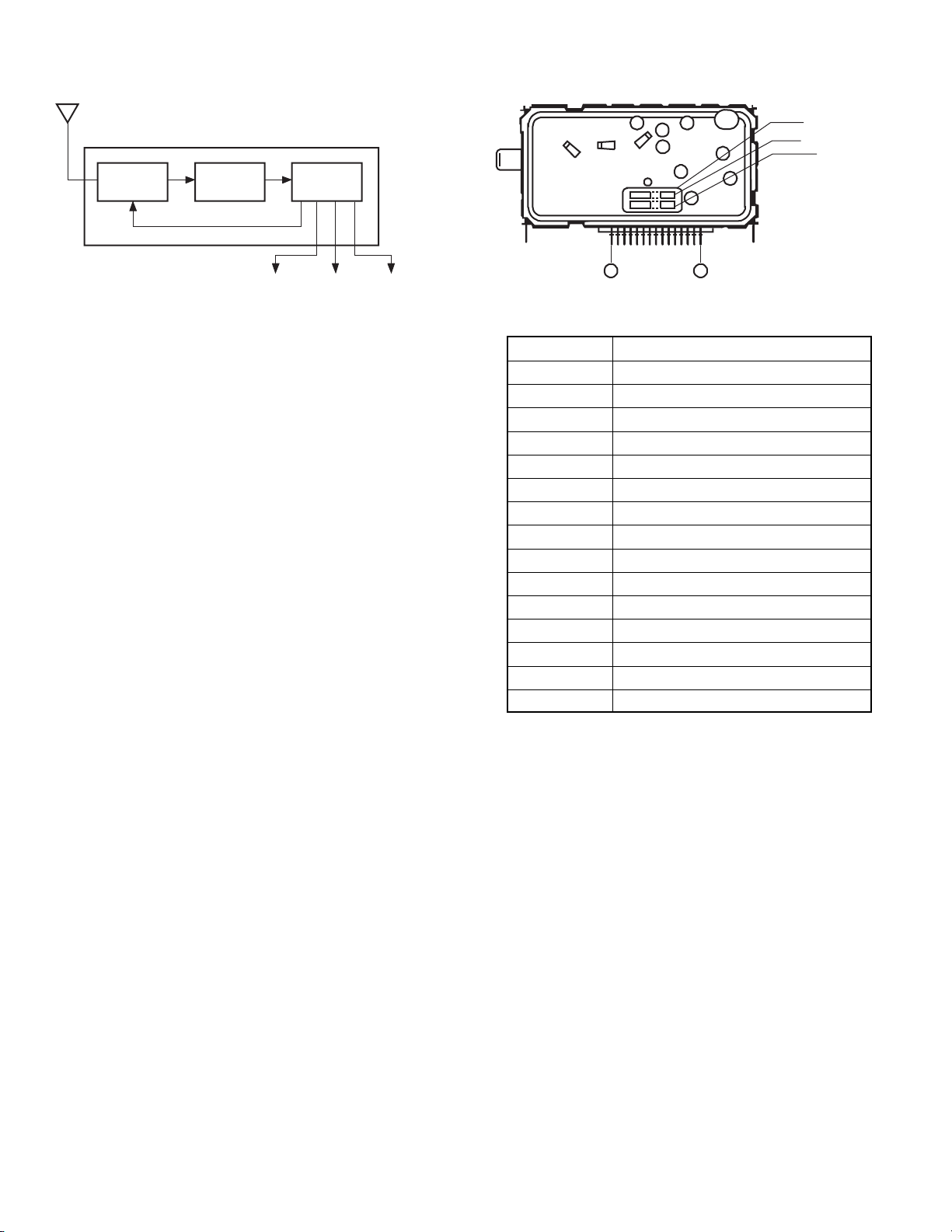
1. OUTLINE OF N5SS CHASSIS
(CN32E90, CN35E90)
The N5SS chassis is a complete bus control type
chassis where the deflection circuit is controlled by a newly
developed I2C-bus line control system.
3. MAJOR SPECIFICATIONS (NEW
FUNCTIONS IN ADDITION TO THOSE
OF N5SS)
(1) EOS (Extended-Data-Service)
(2) Center-Ch-Audio-Input provided
2. PC BOARD CONFIGURATION
(1) Signal unit
(2) Power/def unit
(3) A/V, CRT-D, SP-TERM
(4) CCD, comb (CN32E90)
Digital comb (CN35E90)
(5) D.S.P unit
(6) C.C, EDS/R.G.B SW
4. MODIFICATIONS ON CHASSIS
(1) Serviceability improved with direct, front access system
employed.
(2) One touch cabinet securing (CN32E90) to the chassis.
(3) Improved serviceability with the bus control system
employed for the defection circuits.
(4) Improved serviceability with the white balance bus
control system employed.
(5) Digital comb/CCD miniaturized into a socketable size.
7
5. CONSTRUCTION OF CHASSIS
REAR AMP circuit
SIGNAL circuit
IF/MTS/A-PRO
module
DPC circuit
CCD circuit
PIP circuit
EDS, RGB SW
circuit
AUDIO OUT
CRT circuit
8
Fig. 1-1
POWER/DEF circuit
CONVERTER trans
A/V circuit
RF SW
V. OUT
DPC circuit
H.OUT
H.OUT trans
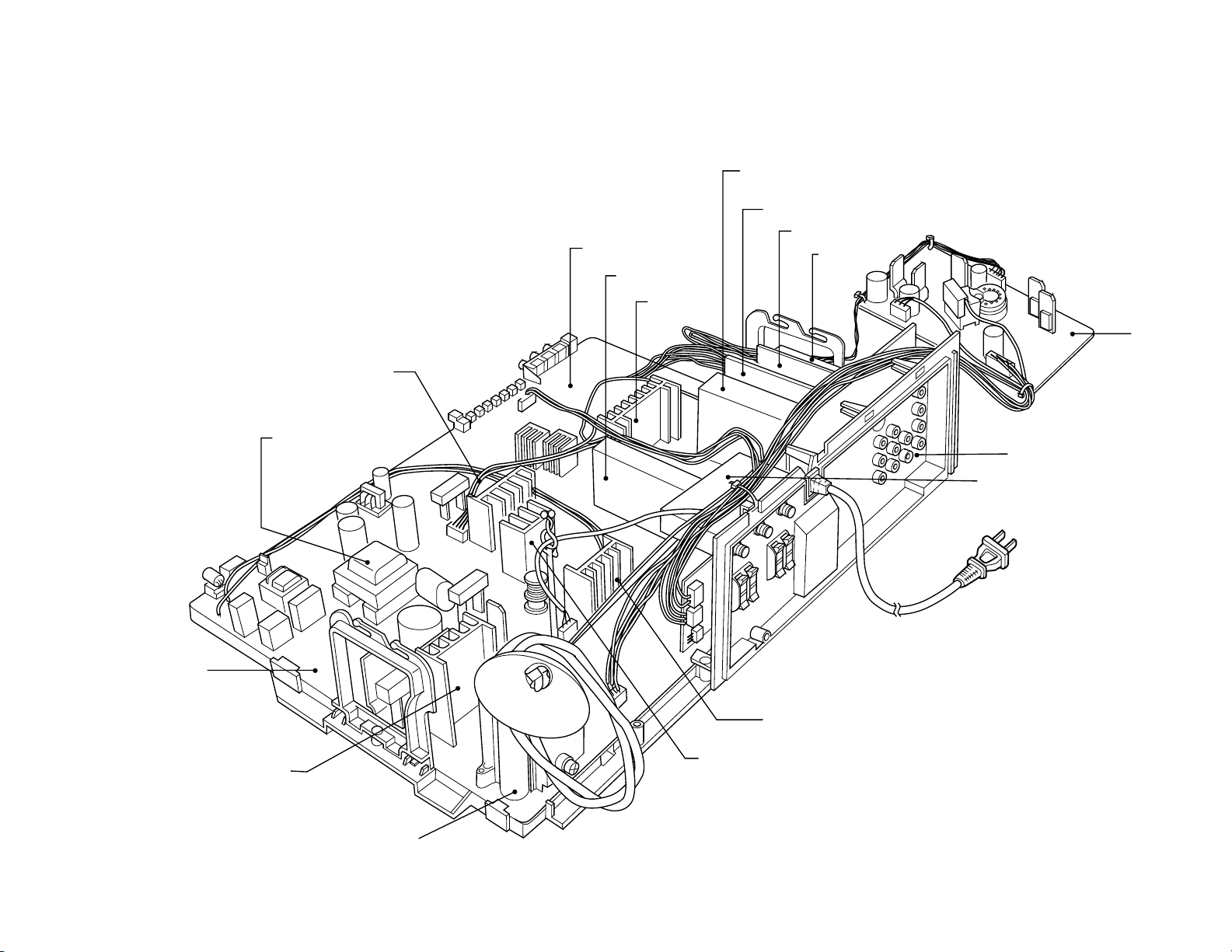
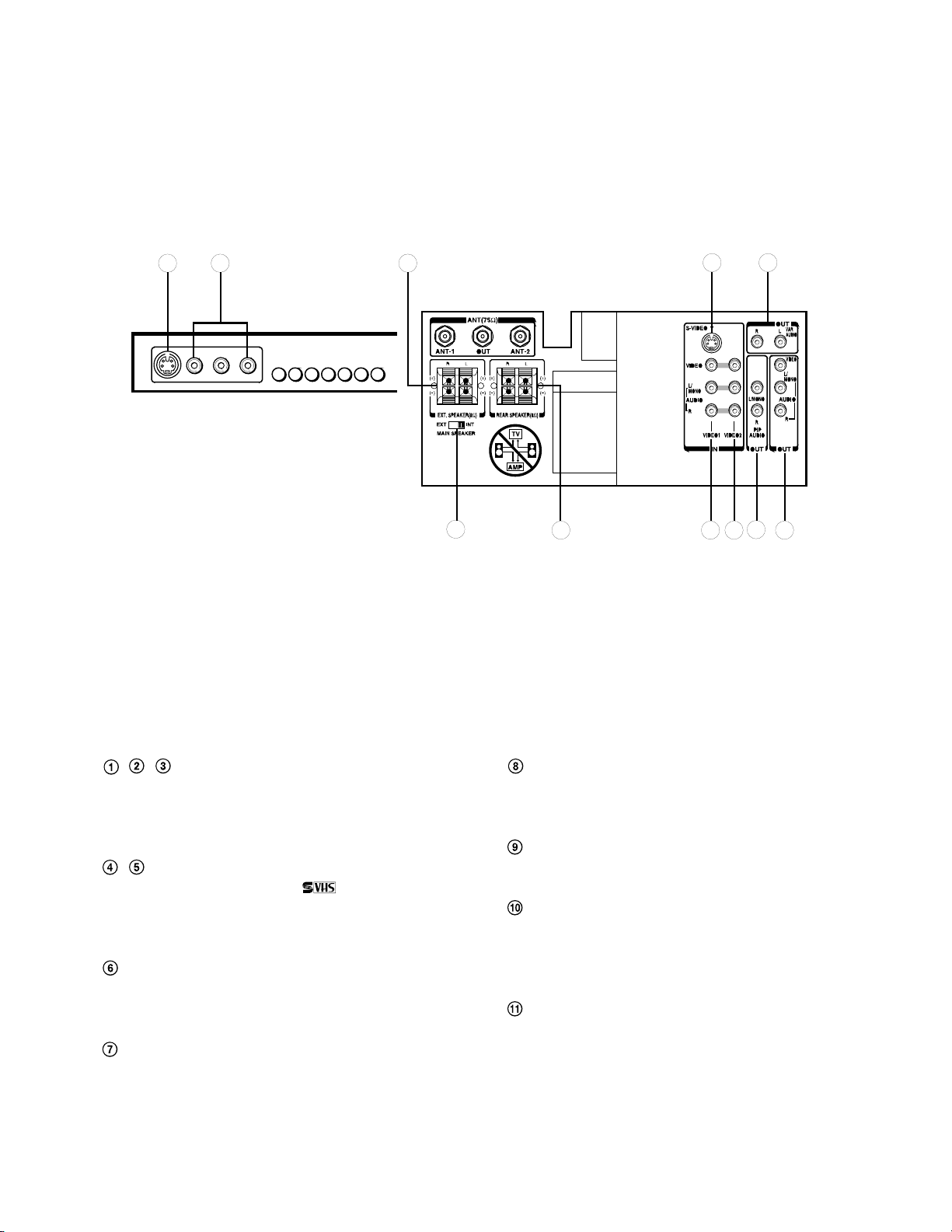
6. LOCATION OF CONTROLS
r
6-1. TV Set
For specific use of each control, consult the corresponding page numbers in brackets.
Front View
POWER indicato
POWER
POWER button
Remote sensor
Behind the door
VIDEO/AUDIO IN
jacks <VIDEO 3>
DEMO button
MENU button
Press to open
the door
CHANNEL
VOLUME
-/+buttons
ANT/VIDEO button
ADV button
buttons
buttons
Fig. 1-2
9
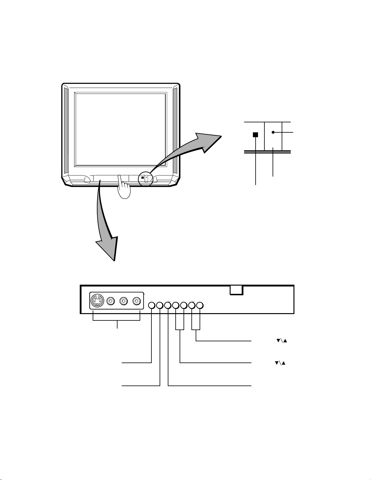
Rear view
t
S-VIDEO IN jack <VIDEO 1>
VARiable AUDIO OUT
ANTenna terminals
EXTernal SPEAKER
erminals
MAIN SPEAKER
switch
REAR SPEAKER
terminals
jacks
VIDEO AUDIO OUT
jacks
PIP AUDIO OUT
jacks
VIDEO/AUDIO IN jacks
<VIDEO 2>
VIDEO/AUDIO IN jacks
<VIDEO 1>
Fig. 1-3
10
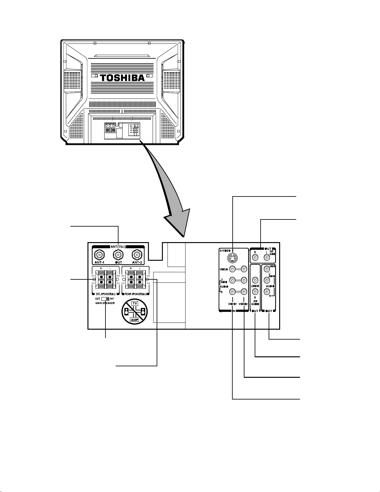
6-2 Location of Controls (Remote Control)
Only the buttons that are used to operate the TV set are described here.
For details on the use of each control, refer to pages in brackets.
Aim at the remote sensor on the TV
Learn/Transmit indicator
EDS button
TV/CABLE/VCR/AUX switch
Set to "TV" to control the TV.
TV/VIDEO
Channel Number buttons
PIP function buttons
AUDio button
PICture button
RESET button
ANT 1/2 button
C.CAPT button
CYS/SBS button
Learning buttons
You can use these eight
buttons only as Learning
function buttons.
They are not affected by
Mode selection (TV/CABLE/
VCR/AUX).
TIMER button
RECALL button
POWER button
MUTE button
CHANNEL buttons
VOLUME buttons
RTN buttons
SET UP button
OPTION button
EXIT button
-\+ buttons
FAV -/+ buttons
DSP/SUR button
DSP F/R button
LEAR/USE switch
To operate buttons inside the cover,
slide the cover down and toward you.
Fig. 1-4
11
6-3 Monitor Panel
This TV set is equipped with S-VIDEO INPUT jacks,
VIDEO/AUDIO INPUT jacks, VIDEO/AUDIO OUTPUT
jacks, VARIABLE AUDIO OUTPUT jacks, PIP AUDIO
OUTPUT jacks and EXTERNAL SPEAKER terminals for
connecting your desired video/audio equipment.
TV Front
935
TV Rear
10
11 1 2
74
8
6
Fig. 1-5
, , VIDEO 1/VIDEO 2/VIDEO 3 IN Jacks —
provide for direct connection of video devices
(VCR, video disc player, camcorder, etc.) with
video/audio outputs.
, S-VIDEO IN Jacks —provide for direct S-video
connection from an
VCR or a video disc
player. The TV's VIDEO 1/3 audio jacks can
also be used to connect the VCR's audio cables.
VIDEO/AUDIO OUT Jacks --- provide fixedlevel audio and video outputs from whatever is
displayed on the screen.
VARIABLE AUDIO OUT Jacks --- feed
volume-controlled stereo audio out from
whatever is displayed on the screen, allows
connection of audio amplifier and lets you adjust
sound level with TV's remote.
12
PIP AUDIO OUT Jacks — provide fixed-level
audio outputs from whatever is displayed on the
PIP window screen.
EXTERNAL SPEAKER Terminals — provide
for direct connection of external speakers.
MAIN SPEAKER Switch — lets you turn off
TV's built-in speakers so that sound will instead
come through speakers connected to
EXTERNAL SPEAKER terminals.
REAR SPEAKER Terminals — provide for
direct connection of the supplied Surround
Speakers.
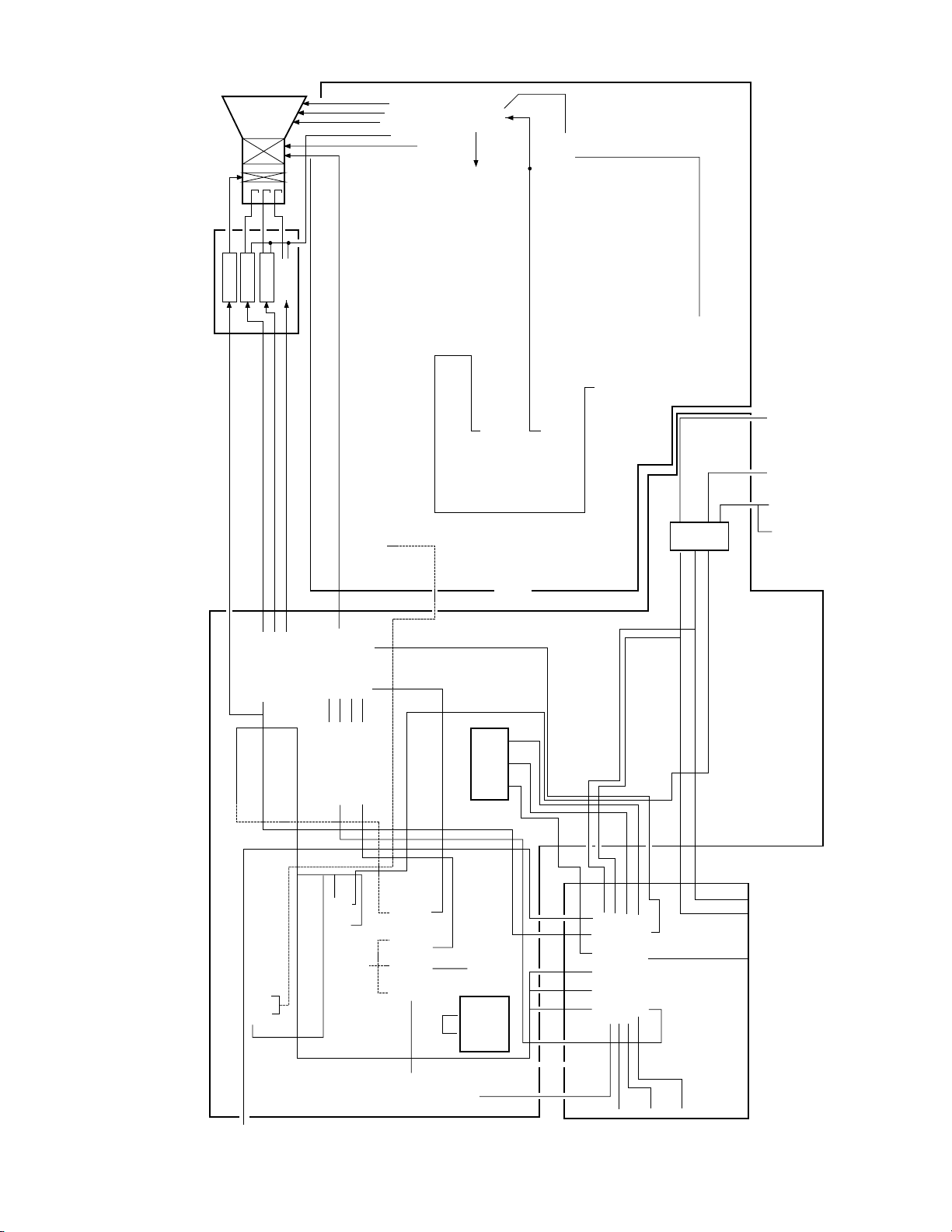
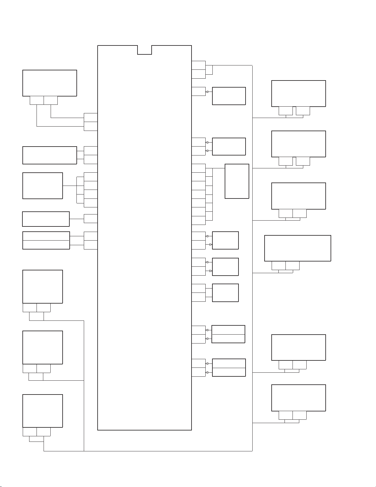
7. CN32D90 BLOCK DIAGRAM
13

8. [US, CANADA] SPECIFICATION FOR MODEL's 1995
CHASSIS C C C C C
MODEL Nbr CN27E90 CX32E70 CN32E90 CE35E15 CF35E50
SPECIFICATION HITACHI TDD TDD *TDD *TDD
1 Picture Tube *FST-D/T NF-D/T NF-D/T *FST-D/T FST-D/T
2 Channel Capacity 181ch 181ch 181ch 181ch 181ch
*
3 C. Caption ●●●●●
G
4 MTS with dbx ●●●●●
E
N
5 Bass, Tre, Balance ●●●●●
E
6 Sub-Audio-Program ●●●●●
R
7 Remote band unit *A-Univ (42k) *A-Univ (42k) *Intelig+EZ *Unive (36k) *Unive (36k)
A
8 Picture-in-Picture ● (2TN) ● (2TN) ● (2TN) *● (1TN) ● (1TN)
L
9 LED Indicators (RED) ● (Power) ● (Power) ● (Power) *● (Power) ● (Power)
10 Local Keys 8key 8key 8key 8key 8key
11 Dolby Surround — — ● ——
12 Dig-Sound Processor — — ● (DSP4ch) — —
*
13 Front Surround ●●—●●
S
14 Cyclone ABX ● — ● ——
O
15 Sub-Bass-System — ● ———
U
16 Audio Output *10Wx2 & 13W 10Wx2 10Wx2 & 10Wx2 10Wx2
N
D
17 Speaker Size & Nbr *80x120x2 70x130x2 80x120x2 70x130x2 70x30x2
18 Comb Filter *● (GLS) ● (CCD) ● (CCD) ● (CCD) ● (GLS)
*
19 Dy-Quadruple Focus — — — — —
P
20 Scan Velocity Modu ●● ●●●
I
21 Vert Contour Corre ●●●● ●
C
22 Black Level Expand ●●●●●
T
23 Flesh Tone Correct *●●●●●
U
R
24 Dynamic Noise Reduc *●●●●●
E
25 Picture Preference ●●●● ●
26 Horiz Resolution 650 700 700 800 800
27 Parental-Ch Lock ●●●●●
*
28 Channel Label (32ch) ●●●●●
O
29 3-Language Display ●●●●●
T
30 Clock/Off-Timer *●/●●/●●/●●/●●/●
H
31 Favorite Channel *● *● *● *● *●
E
R
32 Extended-Data-Servi *● *● *● *● *●
33 Star-Sight-decoder — — — — —
34 S-Video In-Term ● (1+1) ● (1+1) ● (1+1) ● (1) ● (1)
35 Audio, Video-In/Out 1+2/— 1+2/1 1+2/1 *3/1 3/1
*
36 Front AV Jack *●●●——
T
E
37 Variable Audio Out ●●●●●
R
38 2-RF Input ●●●——
M
39 Ext Speaker Term ●●●●●
S
40 PIP Audio Out Jack — *— *● ——
41 Center-Ch-Aud-Input — *● *— — —
42 Speaker-Box -- — ● SS-SR94 — —
*
AC
43 Others — — — — —
*Cabinet NEW CX32D70 CN32D90 *CE35D10 CF35D50
PARTS SUPPLY (ISO) — — — — —
CRT
13W & 5Wx2
& 100R (Hon) 100R & REAR
DERIV
14

CHASSIS C C C C C
MODEL Nbr CX35E60 CX35E70 CX35E81 CN35E90 CN35E95
SPECIFICATION TDD TDD TDD TDD TDD
1 Picture Tube FST-D/T NF-D/T NF-D/T NF-D/T NF-D/T
2 Channel Capacity 181ch 181ch 181ch 181ch 181ch
*
3 C. Caption ●●●●●
G
4 MTS with dbx ●●●●●
E
N
5 Bass, Tre, Balance ●●●●●
E
6 Sub-Audio-Program ●●●●*●
R
7 Remote band unit *A-Univ (42k) *A-Univ (42k) *A-Univ (42k) *Intelig+EZ *Intelig+EZ
A
8 Picture-in-Picture ● (2TN) ● (2TN) ● (2TN) ● (2TN) ● (2TN)
L
9 LED Indicators (RED) ● (Power) ● (Power) ● (Power) ● (Power) ● (Power)
10 Local Keys 8key 8key 8key *8key *8key
11 Dolby Surround — — — ●●
12 Dig-Sound Processor — — — ● (DSP4ch) ● (DSP4ch)
*
13 Front Surround ●●●——
S
14 Cyclone ABX — — — ●●
O
15 Sub-Bass-System ●●●——
U
16 Audio Output 10Wx2 10Wx2 10Wx2 10Wx2 10Wx2
N
D
17 Speaker Size & Nbr 70x130x2 70x130x2 70x130x2 80x120x2 & 80x120x2 &
18 Comb Filter ● (DIG) ● (DIG) ● (DIG) ● (DIG) ● (DIG)
*
19 Dy-Quadruple Focus ●●●●●
P
20 Scan Velocity Modu ●●●●●
I
21 Vert Contour Corre ●●●●●
C
22 Black Level Expand ●●●●●
T
23 Flesh Tone Correct ●●●●●
U
R
24 Dynamic Noise Reduc ●●●●●
E
25 Picture Preference ●●●●●
26 Horiz Resolution 800 800 800 800 800
27 Parental-Ch Lock ●●●●●
*
28 Channel Label (32ch) ●●●●●
O
29 3-Language Display ●●●●●
T
30 Clock/Off-Timer ●/●●/●●/●●/●●/●
H
31 Favorite Channel *● *● *● *● *●
E
R
32 Extended-Data-Servi *● *● *● *● *●
33 Star-Sight-decoder — — — — —
34 S-Video In-Term ● (1+1) ● (1+1) ● (1+1) ● (1+1) ● (1+1)
35 Audio, Video-In/Out 1+2/1 1+2/1 1+2/1 1+2/1 1+2/1
*
36 Front AV Jack ●●●●●
T
E
37 Variable Audio Out ●●●●●
R
38 2-RF Input ●●●●●
M
39 Ext Speaker Term ●●●●●
S
40 PIP Audio Out Jack — *— *— *● *●
41 Center-Ch-Aud-Input — *● *● *— *—
42 Speaker-Box — — — ● SS-SR94 ● SS-SR94
*
AC
43 Others — *VCR-Storate — *VCR-Stora
*Cabinet C35D60 CX35D70 NEW (DAX) CN35D90 NEW (BLK)
PARTS SUPPLY (ISO) — — — — —
CRT
CONSOLE CINEMA
& 13W, 5Wx2 & 13W, 5Wx2
*100R, REAR *120R, REAR
15

SECTION II
TUNER, IF/MTS/S.PRO MODULE
16
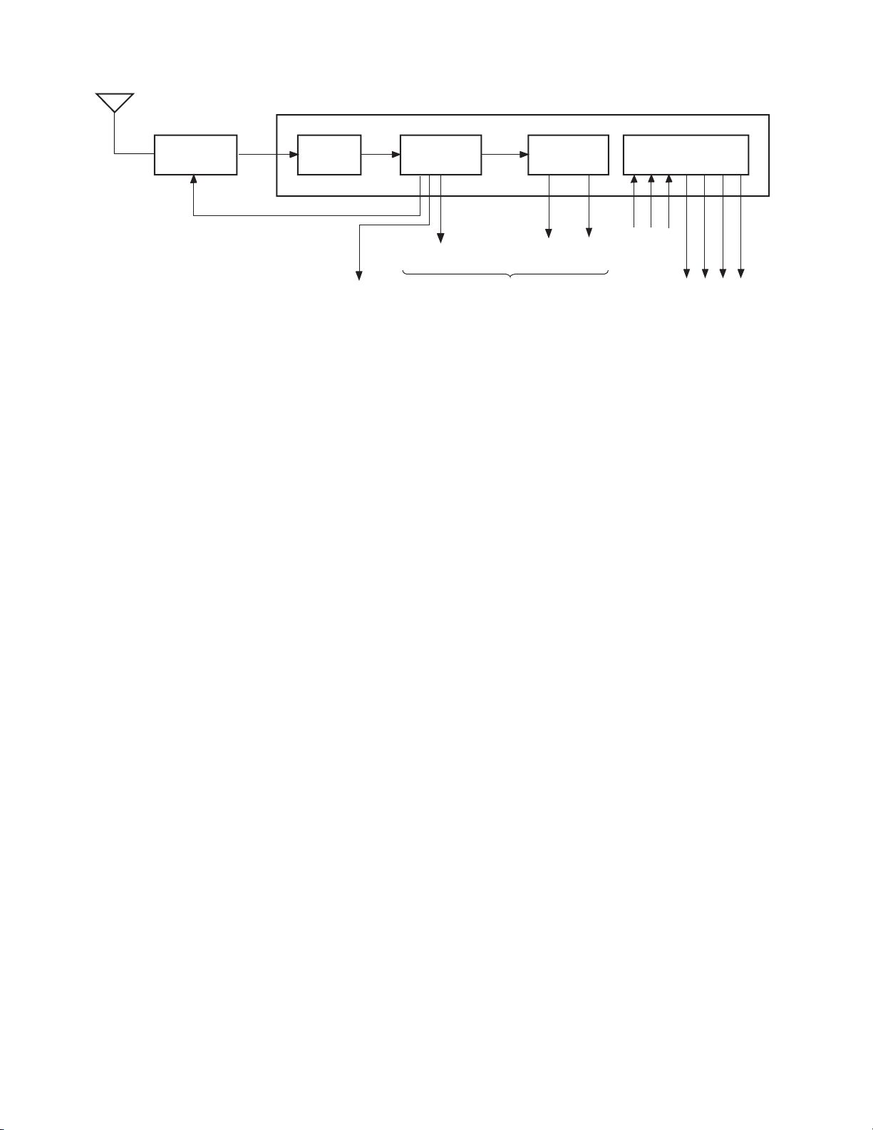
1. CIRCUIT BLOCK
T
EL466L
Tuner
RF AGC
1-1. Outline
IF/MTS/S.PRO Module MVUS34S
SAW
Filter
AFT output
VIF/SIF
Circuit
TP12
Video output
Fig. 2-1 Block diagram
SIF
output
To A/V switch circuit
Multiplex
TV
R-OUTTVL-OUT
Sound
Circuit
C-IN
S.PRO Circuit
R-IN L-IN
R-OUT
L-OUT
(L+R)
-OUT
C-OU
(1) RF signals sent from an antenna are converted into
intermediate frequency band signals (video: 45.75 MHz,
audio: 41.25 MHz) in the tuner. (Hereafter, these signals
are called IF signals.)
(2) The IF signals are band-limited in passing through a
SAW filter.
(3) The IF signals band-limited are detected in the VIF
circuit to develop video and AFT signals.
(4) The band-limited IF signals are detected in the SIF
circuit and the detected output is demodulated by the
audio multiplexer, developing R and L channel outputs.
These outputs are fed to the A/V switch circuit.
(5) A sound processor (S.PRO.) is provided.
1-2. Major Features
(1) The VIF/SIF circuit is fabricated into a small module by
using chip parts considerably.
(2) As the tuner, EL466L that which contains an integrated
PLL circuit is employed.
(3) Wide band double SAW filter F1802R used.
(4) FS (frequency synthesizer) type channel selection system
employed.
(5) VIF/SIF circuit uses PLL sync detection system to
improve performances shown below:
• Telop buzz in video over modulation
• DP, DG characteristics (video high-fidelity
reproduction)
• Cross color characteristic (coloring phenomenon at
color less high frequency signal objects)
(6) HIC SBX1637A-22 is used in the audio multiplexer
circuit to minimize the size with increased performance.
(7) As a sound control processor, TA1217N is used. I
2
Cbus data control the DAC inside the IC to perform
switching of the audio multiplexer modes.
17
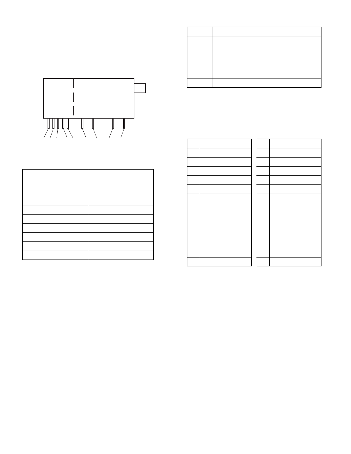
2. TUNER
2-1. Outline
(1) Type name: EL466L
(2) Applicable 181CH
(3) I2C-bus version
(4) PLL-integrated
2-2-2. Terminals (Tuner section)
Name Function
IF OUT IF outputs (P=45.75 MHz, C=42.17 MHz,
S=41.25 MHz)
BM Tuner power supply (9V)
RF AGC Gain control terminal to obtain constant
IF output
VT Control voltage to select channels
PLL Selection
EL466L
Tuner Section
1 2 3 4 5 6 7 8 9
Terminal No. Name
1 32V
25V
3 S-CLOCK
4 S-DATA
5 ADDRESS
6 IF OUT
7 BM (9V)
8 RF AGC
9VT
Fig. 2-2 Tuner terminal layout
2-2-3. Tuner VT Voltage (unit: V)
(1) VHF (2) UHF
CH VT voltage (TYP)
2 1.4
6 6.4
A-2 12.8
B 20.0
C 1.4
I 3.5
10 5.6
J 7.6
N 9.7
R 11.8
W 14.2
FF 17.9
LL 24.2
CH VT voltage (TYP)
MM 1.1
QQ 2.2
WW 4.0
14 5.8
20 7.8
26 9.2
32 10.8
38 12.5
44 13.9
50 15.0
56 17.2
62 19.4
69 23.6
* VT voltage not indicated for a channel falls between
those values for channels just upper and lower the channel.
2-2. Operation of the Tuner
2-2-1. Receiver Channels
VHF 2~13CH
UHF 14~69CH 181CH in total
CATV A-6~, J~W, AA~BBB, 65~92, 100~127CH
18
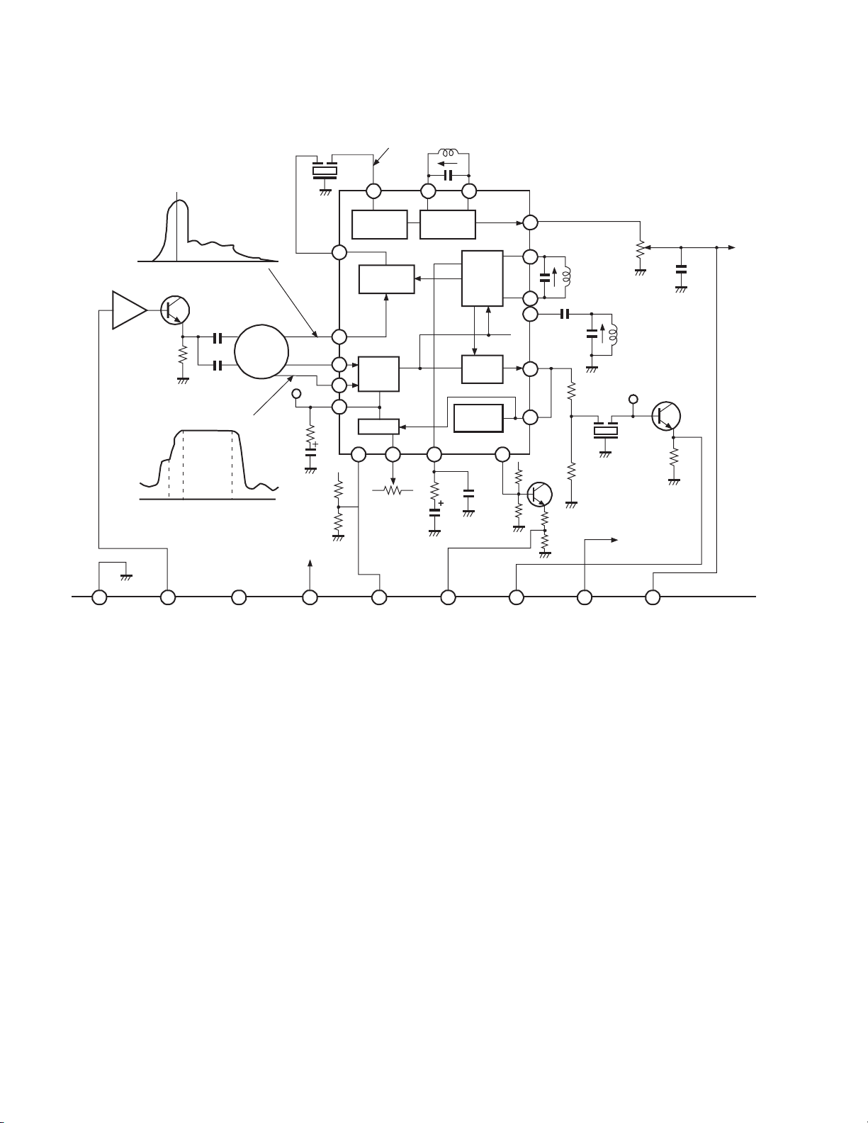
3. IF/MTS/S.PRO MODULE
The IF/MTS/S.PRO module (MVUS34S) limits bandwidth
of IF signals and detects video and audio signals. The module
consists of IF amplifiers, SAW (surface acoustic wave)
filter, and PIF IC. The SAW filter has a wideband response
to improve picture quality and audio buzz characteristic and,
develops separate outputs of video and audio signals. The
PIF IC employs a PLL complete sync detection + audio split
carrier system.
3-1-2 Video PIF Circuit
A PIF detector switching carrier is oscillating at a frequency
adjusted to 45.75 MHz with L051 (VCO CW coil) under no
RF signal input. When an RF signal enters, an IF video
carrier is fed to APC section from IF AMP inside the IC, and
the detector switching carrier is adjusted by the APC, VCO,
etc. in the PLL circuit so that its frequency and phase are
matched to those of the IF video carrier to perform precise
sync detection. Thus processed video output is developed at
pin 21.
3-1. IF/MTS/S.PRO Module (MVUS34S)
3-1-1. Module Terminal Layout
91
27
12
Pin No. Name Pin No. Name
1 GND 15 DAC-OUT2
2 IF-IN 16 R-IN
3 NC 17 C-IN
4 +9V 18 L-IN
5 RF AGC 19 GND
6 AFC 20 SCL
7 VIDEO OUT 21 SDA
8 ADR SW 22 W-OUT
9 MPX OUT 23 C-OUT
10 --- 24 L-OUT
11 --- 25 GND
12 TV R-OUT 26 R-OUT
13 DAC-OUT1 27 +9V
14 TV L-OUT
PLL lock speed is automatically controlled by adding the
video signal at pin 21 to pin 1. That is, since the video signal
is not output at operations of power on, CH switching, etc.,
the APC filter between pin 16 and GND consists of C022 and
C053, and R018, and the filter effect decreases, thus increasing
PLL lock speed.
Next, when a video out exists, the internal resistance is shortcircuited and the APC filter consists of C022 and C053,
internal resistance, and R018. As a result, the filter effect
increases and the PLL lock speed decreases. Consequently,
under normal signal reception, phase of the detector switching
carrier is locked in a stable condition if an IF video carrier is
lost for a short time due to over modulation, etc. By combining
such a PLL complete sync detection system and a wideband
SAW filter shown in Fig. 2-4, a wideband (4.2 MHz) video
detection output with less beat interference will be obtained.
3-1-3. Audio PIF Circuit
The IF signal fed through Q003 (Fig. 2-4) enters an audio
section of the SAW filter (Z001) which has an IF bandwidth
for dedicated audio signals, and only the audio signal of
41.25 MHz is fed to pin 7. The signal is sync-detected with
the detection carrier completely synchronized with the IF
video carrier and pin 14 develops a 4.5 MHz SIF signal. By
using the PLL split carrier system just stated, audio signals
with less buzz by the video signal will be reproduced. The 4.5
MHz SIF enters pin 15 through a 4.5 MHz filter, Z003 and
pin 9 develops a FM-detected audio signal.
Fig. 2-3 IF/MTS/S.PRO module terminal layout
19
SIF BANDWIDTH
M
D
Z003
4.5MHz SIF SIGNAL
15
11 12
FM DET. COIL
L053
9
17.
18
23
21
1
R151
L051
VCO
CW COIL
L502
AFT COIL
TP12
R021
Z002
R022
TO SOUN
MPX IC
C106
Q004
Q002
Q003
IF AMP
GAIN – 14dB
-15dB
S C P
41.25M 45.75M
S
Z001
SAW
FILTER
F1802R
-6dB
SIF LIMIT FM DET.
14.
SIF DET
7
5
IF
AMP
4
22
AGC
2
13 16 20
RF AGC
R051
R018
C053
APC
VCD
VIDEO
DET.
LOCK
CONTROL
C022
VIDEO IF BANDWIDTH
1 2
3
4 5 6
7
8
9
GND IF-IN N.C +B(9V) RF AGC AFC VIDEO OUT ADR SW
Fig. 2-4 IF/MTS/S. PRO circuit diagram
20
3-1-4. Audio Multiplex Demodulation Circuit
The sound multiplex composite signal FM-detected in the
PIF circuit enters pin 12 of HIC (hybrid IC) in passing
through the separation adjustment VR RV2 and amplified.
After the amplification, the signal is split into two: one enters
a de-emphasis circuit, and only the main signal with the LR signal and a SAP signal removed enters the matrix circuit.
At the same time, the other passes through various filters and
trap circuits, and the L-R signal is AM-demodulated, and the
SAP is FM-demodulated.
MVUS32S
Then, both are fed to the matrix circuit. At the same time,
each of the stereo pilot signal fH and the SAP pilot signal 5fH
is also demodulated to obtain an identification voltage. With
the identification voltage thus obtained and the user control
voltage are used to control the matrix.
The audio signals obtained by demodulating the sound
multiplex signal develop at pin 10 and 11 of HIC and develop
the terminals of 12 and 14 of the module.
MPX
Out
9
Monitor the input
pin for multiplex
sound IC
10
Stereo 0V
Other 0V
Fig. 2-5 Block diagram of MVUS32S
Table 2-1 Matrix for broadcasting conditions and
reception mode
Output OSD display
Broad- Switching
casted mode
12 pin 14 pin
(R) (L)
Stereo SAP
Stereo STE R L O X
SAP R L O X
MONO L+R L+R O X
Mono STE L+R L+R X X
SAP L+R L+R X X
MONO L+R L+R X X
Stereo STE R L O O
+ SAP SAP SAP O O
SAP MONO L+R L+R O O
Mono STE L+R L+R X O
+ SAP SAP SAP X O
SAP MONO L+R L+R X O
DAC-out1 DAC-out2
TV TV
(SURR OFF)
R-Out
11
SAP 0V
Other 0V
TV waveform detection
12 13 14
OFF 0V
ON 9V
Not used for
CN32E90.
output (R)
To AV select circuit
Note:
Of the mode selection voltages, switching voltages for STE,
SAP, MONO do not output outside the module.
They are used inside the module to control the BUS.
L-Out
TV waveform detection
output (L)
(RFSW)
14
RF1 0V
RF1 9V
21
3-1-5. A.PRO Section (Audio Processor)
The S.PRO section has following functions.
(1) Woofer processing (L+R output)
(2) High band, low band, balance control
(3) Sound volume control, cyclone level control
(4) Cyclone ON/OFF
TA1217N
All these processing are carried out according to the BUS
signals sent from a microcomputer.
Fig. 2-6 shows a block diagram of the A.PRO IC.
Lin
Rin
Cin
Win
SDA
SGL
1272922 32
30
34
2
3
20
21
TONE CONTROL
LPF
4
33
Center
LEVEL
Woofer
LEVEL
2
I C
56 73124
D/A
CONV
VOLUME
23 22 19
30 9 8 28
BALANCE
I/O
26
Lout
Rout
25
Cout
18
Wout
10
17
16
15
14
13
12
11
SAP det.
STE det.
16
R-in C-in L-in
From From From
A/V Dolby A/V
18 19 20 21 22
17
24
23
SCL SDA W-out O-out L-out R-out
Q670 Q640 Q670 Q670
Via QS101
26 27
25
Fig. 2-6 A.PRO block diagram
22
9V
4. PIP TUNER
Lable
Name
Lot No.
1
15
TUNER
SECTION
RF AGC
SAW
FILTER
AFT
OUTPUT
VIF/SIF
CIRCUIT
VIDEO
OUTPUT
AUDIO
OUTPUT
Fig. 2-7
4-1. Outline
The PIP tuner (EL922L) consists of a tuner and an IF block
integrated into one unit. The tuner receives RF signals
induced on an antenna and develops an AFT output, video
output, and audio output.
The tuner has receive channels of 181 as in the tuner for the
main screen and it is also controlled through the I2C-bus.
As the IC for the IF, a PLL complete sync detection plus
audio inter carrier system are employed.
Terminal No. Name
1NC
2 32V
3 S-CLOCK
4 S-DATA
5NC
6 ADDRESS
75V
8 RF AGC
99V
10 AUDIO
11 GND
12 AFT
13 NC
14 GND
15 VIDEO
Fig. 2-8 Tuner terminal layout
23

SECTION III
CHANNEL SELECTION CIRCUIT
24

1. OUTLINE OF CHANNEL SELECTION
CIRCUIT SYSTEM
The channel selection circuit in the N5SS chassis employs
a bus system which performs a central control by connecting
a channel selection microcomputer to a control IC in each
circuit block through control lines called a bus. In the bus
system which controls each IC, the I2C bus system (two line
bus system) developed by Philips Co. Ltd. in the Netherlands
has been employed.
The ICs controlled by the I2C bus system are : IC for audio
signal processing (QN06), IC for V/C/D signal processing
(Q501), IC for A/V switching (QV01), IC for non volatile
memory (QA02), Main and sub U/V tuners (H001, HY01),
IC for deflection distortion correction (Q302), IC for PIP
signal processing (QY04), IC for DSP (QM01), IC for
closed caption control (Q701).
Differences from N4SS chassis are as follows;
1. On-screen function inside microcomputer is used.
Separate IC is not used for on-screen.
2. The microcomputer does not have the closed caption
function, but controls separate IC for closed caption.
3. The system uses two channels of I2C bus. One is only
for non-volatile memory.
2. OPERATION OF CHANNEL
SELECTION CIRCUIT
Toshiba made 8 bit microcomputer TLCS-870 series for TV
receiver, TMP87CS38N-3152 is employed for QA01.
With this microcomputer, each IC and circuit shown below
are controlled.
(1) CONTROL OF AUDIO SIGNAL PROCESS IC (QN06
Toshiba TA1217N)
• Adjustments for volume, treble, bass and balance
• Selection between surround mode and DSP mode,
and level adjustment
• Level adjustment of BAZOOKA system
• Audio muting during channel selection or no signal
reception.
(2) CONTROL OF VIDEO/CHROMA/DEF SIGNAL
PROCESS IC (Q501 Toshiba TA1222N)
• Adjustments for uni-color, brightness, tint, color
gain, sharpness and PIP uni-color
• Setting of adjustment memory values for subbrightness, sub-color and sub-tint, etc.
• Setting of memory values for video parameters
such as white balance (RGB cutoff, GB drive) and
gcorrection, etc.
• Setting of video parameters of video modes
(Standard, Movie, Memory)
(3) CONTROL OF A/V SWITCH IC (QV01 Toshiba
TA1219N)
• Preforms source switching for main screen and
sub screen
• Performs source switching for TV and three video
inputs
(4) CONTROL OF NON-VOLATILE MEMORY IC
(QA02 Microchip 24LC04BI/P)
• Memorizes data for video and audio signal
adjustment values, volume and woofer adjustment
values, external input status, etc.
• Memorizes adjustment data for white balance
(RGB cutoff, GB drive), sub-brightness, sub color,
sub tint, etc.
• Memorizes deflection distortion correction value
data adjusted for each unit.
(5) CONTROL OF U/V TUNER UNIT (H001 Matsushita
EL466L, HY01 Toshiba EL922L)
• A desired channel can be tuned by transferring a
channel selection frequency data (divided ratio
data) to the I2C bus type frequency synthesizer
equipped in the tuner, and by setting a band switch
data which selects the UHF or VHF band.
(6) CONTROL OF DEFLECTION DISTORTION
CORRECTION IC (Q302 Toshiba TA8859P)
• Sets adjustment memory value for vertical
amplitude, linearity, horizontal amplitude,
parabola, corner, trapezoid distortion.
(7) CONTROL OF PIP SIGNAL PROCESS IC (QY04
Toshiba TC9083F)
• Controls ON/OFF and position shift of PIP.
(8) CONTROL OF DIGITAL SOUND PROCESSOR IC
(QM04 Yamaha YSS238-D)
• Performs mode switching of DSP.
(9) CONTROL OF CLOSED CAPTION/EDS (QM01
Motorola XC144144P)
• Controls Closed Caption/EDS.
25
3. MICROCOMPUTER
SDA
SCL
1 - 7
8
9 1 - 7
8
9
1 - 7
8
9
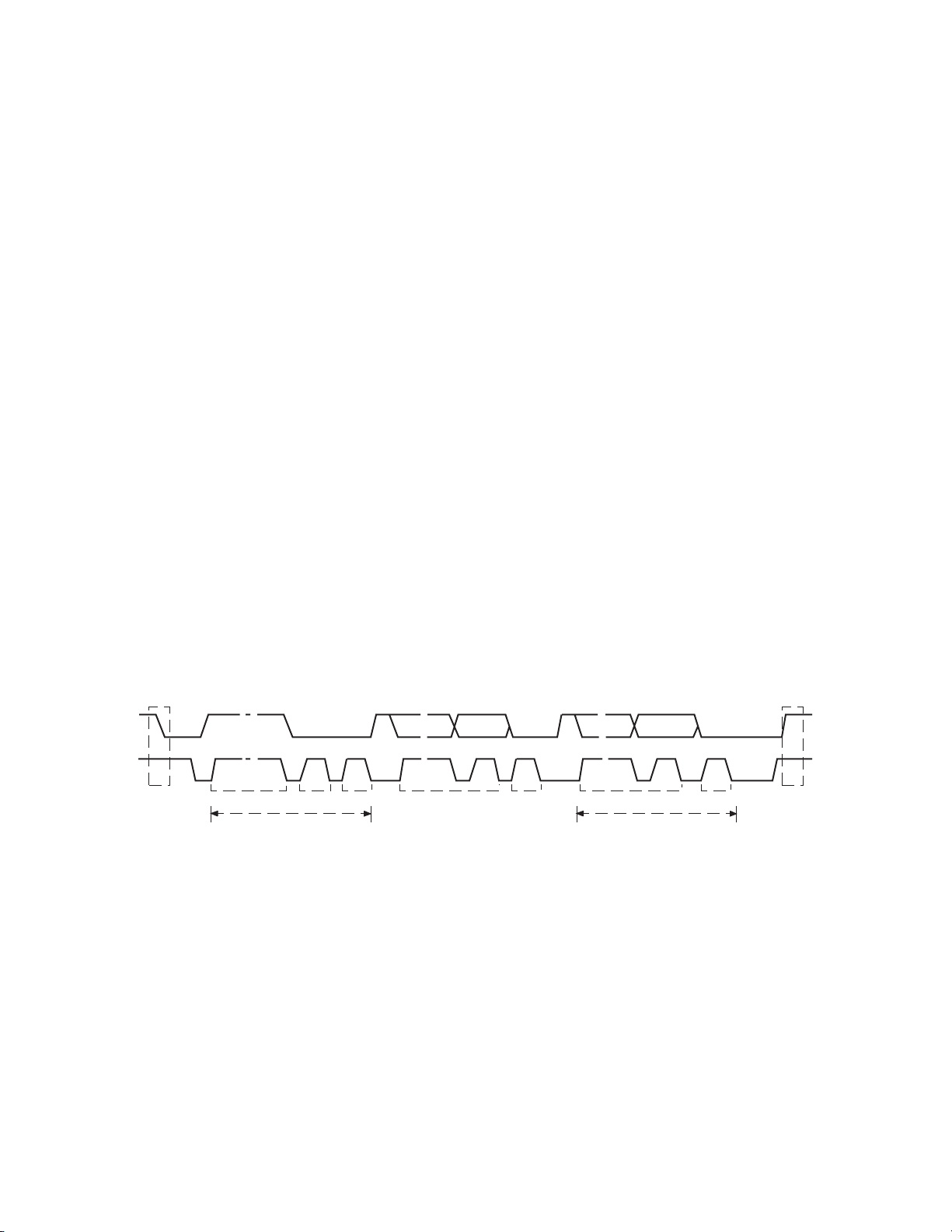
START
CONDITION
STOP
CONDITION
ADDRESS
R/W
Ack DATA
Ack
DATA Ack
Approx.180
m
S
Some device may have no data,
or may have data with several
bytes continuing.
Microcomputer TMP87CS38N-3152 has 60k byte of ROM
capacity and equipped with OSD function inside.
The specification is as follow.
• Type name : TMP87CS38N-3152
• ROM : 60k byte
• RAM : 2k byte
• Processing speed : 0.5m s (at 8MHz with Shortest
command)
• Package : 42 pin shrink DIP
• I2C-BUS : two channels
• PWM : 14 bit x 1, 7 bit x 9
• ADC : 8 bit x 6 (Successive comparison system,
Conversion time 20ms)
• OSD
Character kinds : 256
Character display : 24 characters x 12 lines
Character dot : 14 x 18 dots
Character size : 3 kinds (Selected by line)
Character color : 8 colors (Selected by character)
Display position : Horizontal 128 steps, Vertical
256 steps
This microcomputer performs functions of AD converter,
reception of U/V TV and OSD display in one chip.
IIC device controls through I2C bus. (Timing chart : See fig.
3-1)
• LED uses big current port for output only.
• For clock oscillation, 8MHz ceramic oscillator is used.
• I2C has two channels. One is for EPROM only.
• Self diagnosis function which utilizes ACK function of
I2C is equipped
• Function indication is added to service mode.
• Remote control operation is equipped, and the control
by set no touch is possible. (Bus connector in the
conventional bus chassis is deleted.)
• Substantial self diagnosis function
(1) B/W composite video signal generating function
(micom inside, green crossbar added)
(2) Generating function of audio signal equivalent
to 1kHz (micom inside)
(3) Detecting function of power protection circuit
operation
(4) Detecting function of abnormality in IIC bus
line
(5) Functions of LED blink indication and OSD
indication
(6) Block diagnosis function which uses new VCD
and AV SW
Fig. 3-1
26
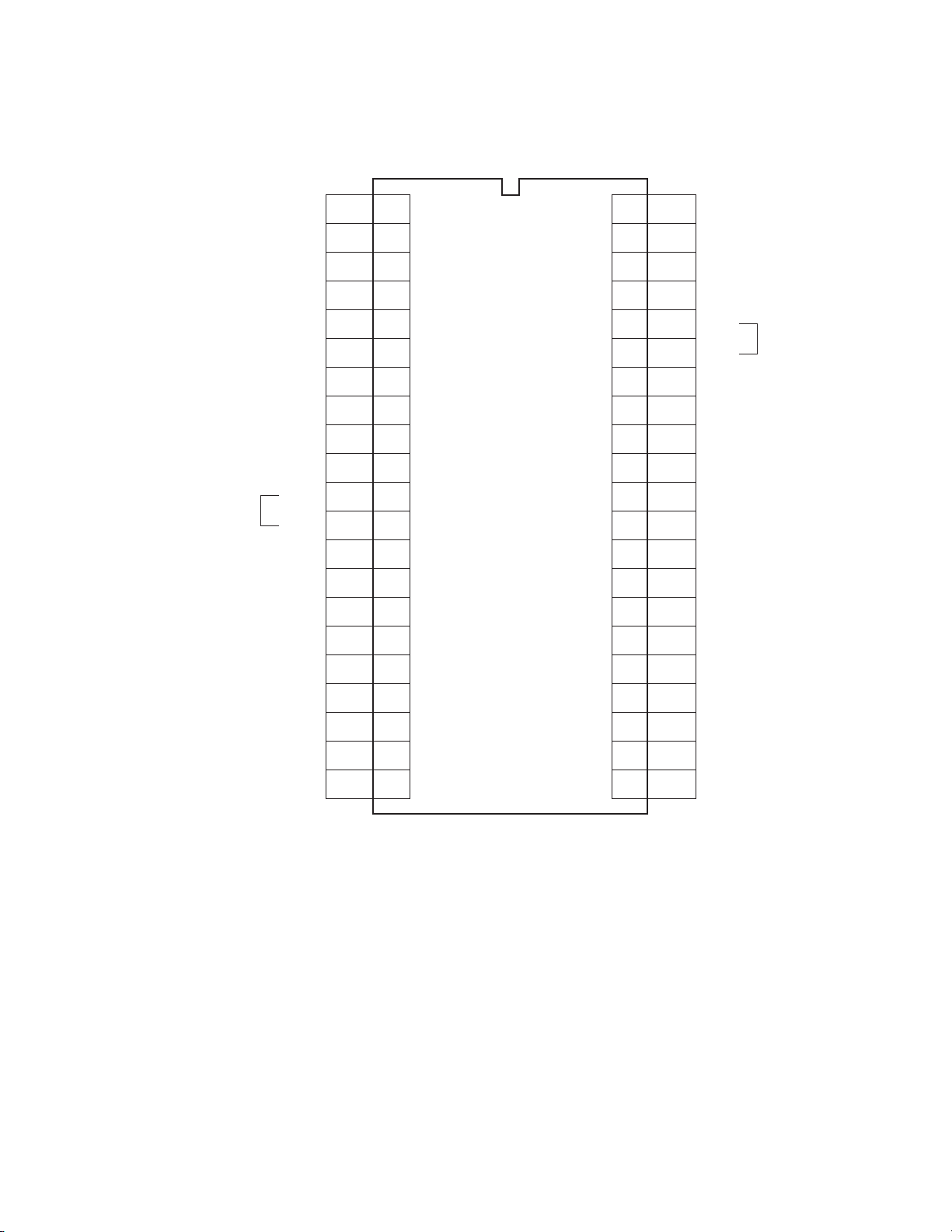
4. MICROCOMPUTER TERMINAL FUNCTION
TMP87CS38N3152 (QA01)
GND
1
GND
VDD
42
VDD
IIC
-BUS
BAL
REM OUT
MUTE
SP MUTE
NC
POWER
LED
NC
NC
SCL0
SDA0
SYNC VCD
NC
AFT2
AFT1
KEY-A
KEY-B
SGV
SGA
GND
10
11
12
13
14
15
16
17
18
19
20
21
2
I
P40 (PWM0)
3
O
P41 (PWM1)
4
O
P42 (PWM2)
5
O
P43 (PWM3)
6
O
P44 (PWM4)
7
O
P45 (PWM5)
8
O
P46 (PWM6)
9
O
P47 (PWM7)
I
P50 (PWM8/TC2)
O
P51 (SCL1)
IO
P52 (SDA1)
I
P53 (AINO/TC1)
I
P54 (AIN1)
I
P55 (AIN2)
I
P56 (AIN3)
I
P60 (AIN4)
I
P61 (AIN5)
O
P62
O
P63
VSS
P57
P32
P57
SDA0
SCL0
(TC3)P31
(RXIN)P30
P20
RESET
XOUT
XIN
TEST
0SC2
0SC1
VD
HD
Y/BL
I
IO
O
I
I
I
I
O
I
I
O
I
I
I
O
O
B
O
G
O
R
41
40
39
38
37
36
35
34
33
32
31
30
29
28
27
26
25
24
23
22
ACP
NC
GND
SDA1
SCL1
SYNC AV1
RMT IN
SW IN
RESET
XOUT
XIN
TEST
0SC1
0SC2
VSYNC
HSYNC
Ys
BOUT
GOUT
ROUT
IIC BUS
Fig. 3-2
27

<< MICROCOMPUTER TERMINAL NAME AND OPERATION LOGIC >>
No. Terminal Name Function In/Out Logic Remarks
1 GND 0V
2 BAL INPUT BALANCE Out PWM out
3 REM OUT REMOTE CONTROL Out Remote control output
SIGNAL OUT
4 MUTE SOUND MUTE OUT Out Sound mute output
5 SP MUTE SPEAKER MUTE Out In muting = H
6 DEF POW Out
7 POWER POWER ON/OFF OUT Out Power control In ON=H
8 LED POWER LED OUTPUT Out Power LED on-control
LED lighting=L
9 POWER LNB Out 0V
10 LNB DET In 0V
11 SCL() IIC BUS CLOCK OUT Out IIC bus clock output 0
12 SDA() IIC BUS DATA IN/OUT In/Out IIC bus data input/output 0
13 SYNC VCD H SYNC INPUT In Main picture H. sync signal input
14
15 AFT2 IN In Sub tuner AFT S-curve input
16 AFT1 UV MAIN S-CURVE In Main tuner AFT S-curve
SIGNAL signal input
17 KEY A LOCAL KEY INPUT In Local key detection: 0 to 5V
18 KEY B LOCAL KEY INPUT In Local key detection: 0 to 5V
19 SGV TEST SIGNAL OUT Out Test signal output In normal=L 0V
20 SGA TEST AUDIO OUT Out Test audio output In normal=L 0V
21 VSS POWER GROUNDING — 0V: Gounding voltage 0V
22 R R Out At display on:Pulse
23 G G Out At dispaly on:Pulse
24 B B Out At dispaly on:Pulse
25 Y/BL BL Out At dispaly on:Pulse
26 HSYNC In HSYNC for OSD display Pulse
27 VSYNC In VSYNC for OSD display Pulse
28 OSC1 DISPLAY CLOCK Out 4.5MHz Pulse
29 OSC2 DISPLAY CLOCK In Pulse
30 TEST TEST MODE In GND fixed 0V
31 XIN SYSTEM CLOCK In System clock input 8MHz pulse
32 XOUT SYSTEM CLOCK Out System clock output 8MHz 8MHz pulse
33 RESET SYSTEM RESET In System reset input (In reset=L) 5V
34 SW IN
35 RMT IN REMOTE CONTROL IN In remote control pulse input=L In reception of
SIGNAL INPUT remote pulse
36 SYNC AV1 HSYNC INPUT In External H. sync signal input Pulse
37 SCL1 IIC BUS CLOCK OUT Out IIC bus clock output 1 Pulse
38 SDA1 IIC BUS DATA IN/OUT In/Out IIC bus data input/output 1 Pulse
39 GND 0V
40 NC
41 ACP NSYNC INPUT In AC pulse input
42 VDD POWER — 5V 5V
28
5. EEPROM (QA02)
EEPROM (Non volatile memory) has function which, in spite of power-off, memorizes the such condition as channel selecting
data, last memory status, user control and digital processor data. The capacity of EEPROM is 8k bits. Type name is 24LC04BI/
P or ST24C04CB6, and those are the same in pin allocation and function, and are exchangeable each other. This IC controls
through I2C bus. The power supply of EEPROM and MICOM is common. Pin function of EEPROM is shown in Figure 3-3.
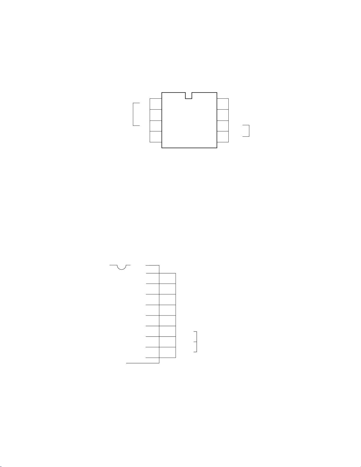
EEPROM(QA02)
1
Device adress
GND
A0
A1
A2
Vss
2
3
4
Fig. 3-3
8
7
6
5
Vcc + 5V
NC
SCL
SDA
2
C-BUS line
I
6. ON SCREEN FUNCTION
ON SCREEN FUNCTION indicates data like channel, volume. Formerly, exclusive use of OSD IC was used, but in N5SS,
OSD function is involved in microcomputer. Pin function concerning on-screen is shown in figure 3-4. Oscillation clock of OSD
is approx. 4.5MHz. 9MHz which becomes twice in microcomputer is dot clock. For oscillation coil, TRF1160D (LA02) is used.
QA01
OSC2
OSC1
VD
HD
Y/BL
O
29
OSC2 OSC OUT
I
28
OSC1 OSC IN
I
27
VSYNC H. SYNC SIGNAL
I
26
HSYNC V. SYNC SIGNAL
O
25
Ys/Ym HALF TONE SIGNAL
B
O
G
O
R
O
BOUT
24
23
GOUT COLOR SIGNAL
22
ROUT
G
V
Fig. 3-4
29
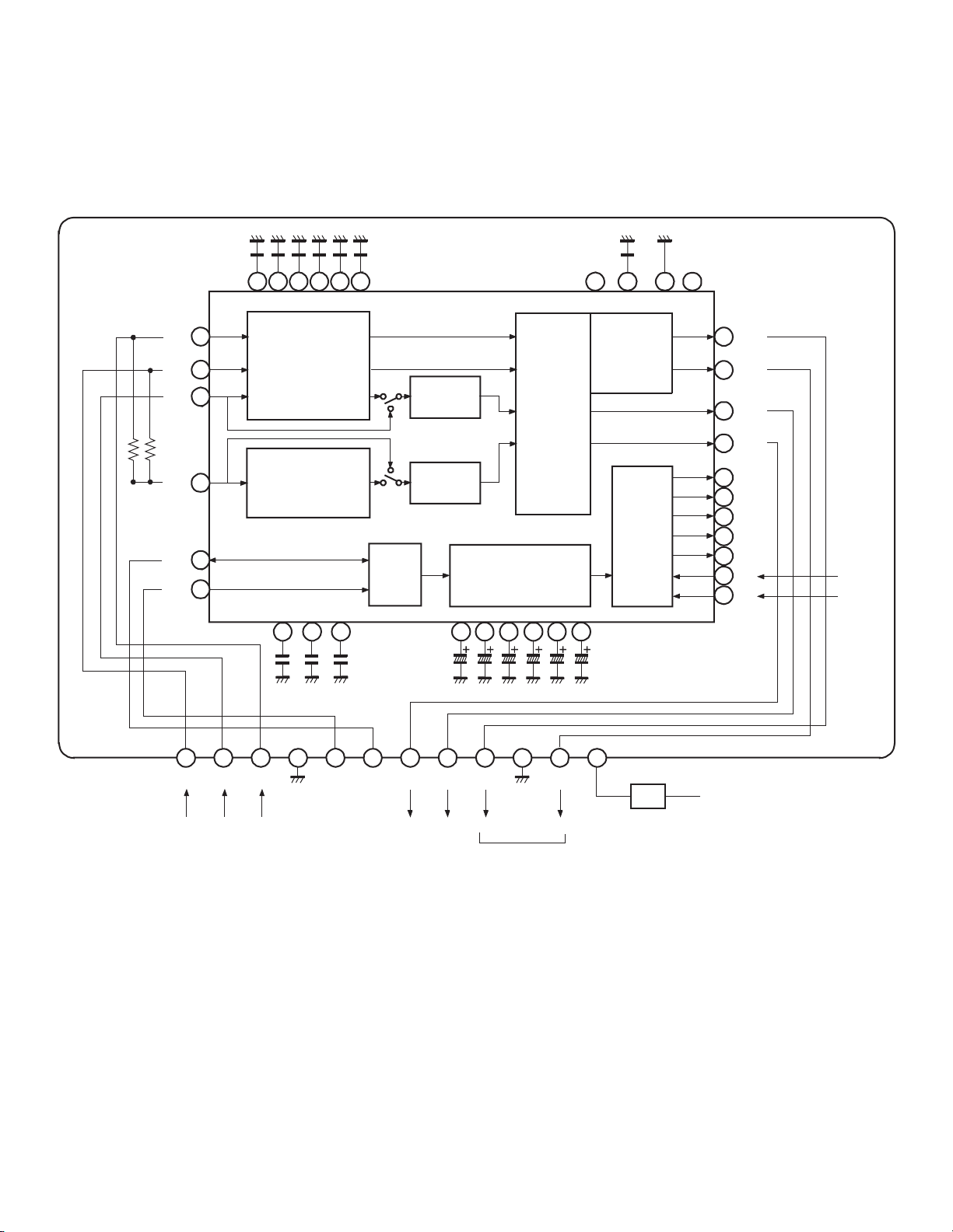
7. SYSTEM BLOCK DIAGRAM
TMP87CS38N-3152
QA01
QA02
MEMORY
24LC04B1/P
SDA SCL
5 6
H. SYNC PULSE
VSYNC PULSE
VIDEO SIGNAL
PROCESS
CIRCUIT
REMOTE CONTROL
OUTPUT
SOUND MUTE
SPEAKER MUTE
Q701
C/C, EDS
XC144144P
DATA CLK
11
12
26
27
22
23
24
25
3
4
5
SCL 0
SDA 0
HSYNC
VSYNC
R
G
B
YS/TM
RMT OUT
MUTE
SP MUTE
SDA 1
SCL 1
RMT
KEY-A
KEY-B
RST
VDD
GND
VSS
POWER
ACP
LED
XIN
XOUT
OSCI
OSCO
SGV
SGA
38
37
35
17
18
33
42
21
41
31
32
28
29
19
20
1
7
8
REMOTE
SENSOR
UNIT
KEY SWITCH
POWER
SUPPLY
CIRCUIT
8MHz
CLOCK
6.1MHz
CLOCK
SIGNAL
OUTPUT
H001
MAIN U/V TUNER
EL446L
SDA SCL
HY01
SUB U/V TUNER
EL922L
SDA SCL
Q501
VCD
TA1222
SDA SCL
27 28
H002
IF/MPX
MVUS345
SDA SCL
21 20
DPC UNIT
DATA CLK
QY04
PIP CONTROL
DATA CLK
6 5
SYNC-AV1
AFT1 IN
SYCN-AV2
AFT2 IN
36
16
13
Fig. 3-5
30
MAIN SCREEN
SUB SCREEN
2
SYNC DET.
AFT DET.
SYNC DET.
AFT DET.
QV01
AV SW
TA1219N
SDA SCL
26 27
QM01
DSP
SDA SCL

8. LOCAL KEY DETECTION METHOD
15 16
S15-1
S16-1
Local key detection in the N5SS chassis is carried out by
using analog like method which detects
a voltage appears at local key input terminals (pins 17, 18) of
the microcomputer when a key is
pushed. With this method using two local key input terminals
( pins 17,18), key detection up to
maximum 14 keys will be carried out.
S15-2
S15-3
S15-4
S15-5
S15-6
S15-7
Fig. 3-6. Local key assignment
S16-2
S16-3
S16-4
S16-5
S16-6
S16-7
The circuit diagram shown left is the local key circuit. As can
be seen from the diagram, when
one of key among SA-01 to SA-08 is pressed, each of two
input terminal (pins 17, 18) developes
a voltage Vin corresponding to the key pressed. (The voltage
measurement and key identification
are carried out by an A/D converter inside the microcomputer
and the software.
Key No. Function Key No. Function
SA-02 POWER SA-01
DEMO START/STOP
SA-03 CH UP
SA-04 CH DN
SA-05 VOL UP
SA-06 VOL DN
SA-07 ANT/VIDEO, ADV
SA-08 MENU
Table 3-1. Local key assinment
31

9. REMOTE CONTROL CODE ASSIGNMENT
Custom codes are 40-BFH
Code
00H 0 Channel
01H 1 Channel
02H 2 Channel
03H 3 Channel
04H 4 Channel
05H 5 Channel
06H 6 Channel
07H 6 Channel
08H 8 Channel
09H 8 Channel
0AH 100 Channel
0BH ANT 1/2
0CH RESET
0DH AUDIO
0EH PICTURE/FUNC
0FH TV/VIDEO
10H MUTE
11H CHANNEL SEARCH
12H POWER
13H MTS
14H ADD/ERASE
15H TIMER/CLOCK
16H AUTO PROGRAM
17H CHANNEL RETURN
18H DSP/SUR (TV/CATV)
19H CONTROL UP
1AH VOLUME UP
1BH CHANNEL UP
1CH RECALL
1DH CONTROL DOWN
1EH VOLUME DOWN
1FH CHANNEL DOWN
40H PIP LOCATE
41H PIP LOCATE
42H PIP LOCATE
43H PIP LOCATE
44H CARVER
45H SURROUND UP
46H SURROUND DOWN
47H VOCAL ZOOM
48H CHANNEL LOCK
49H
4AH PIP CHANNEL UP
4BH
4CH
4DH
4EH PIP LOCATE
4FH PIP SOURCE
Function to remote
PIP CHANNEL DOWN
PIP STILL/RELEASE
PIP ZOOM, ZOOM SIZE
Applicable
control
Applicable Conti-
to TV set nuty
Custom codes are 40-BFH
Code
50H PIP STILL
51H PIP ON/OFF
52H Do not use. Old type core power ON
53H PIP SWAP
54H PIC SIZE
55H DSP F/R
56H WIDE/SCROLL
57H CAPTION
58H EXIT
59H CYCLONE, SBS
5AH SER UP
5BH OPTION
5CH SUB WOOFER UP
5DH
SUB WOOFER DOWN
5EH
5FH
80H MENU
81H EDS
82H ADV UP
83H ADV DWN
84H
85H
86H
87H
88H PIP CONTROL
89H
8AH
8BH
8CH
8DH
8EH
8FH
90H
91H
92H
93H
94H Do not use. Old type core power ON
95H
96H
97H NOISE CLEAN
98H
99H
9AH PIP VOLUME UP
9BH
9CH PIP CONTROL
9DH
9EH
PIP VOLUME DOWN
9FH
Function to remote
Applicable
control
Applicable Conti-
to TV set nuty
32

Custom codes are 40-BFH
Code
Function to remote
Applicable
control
C0H
C1H
C2H
C3H
C4H PIP LOCATE
C5H PIP LOCATE
C6H PIP LOCATE
C7H PIP LOCATE
C8H PIP STROBE
C9H PIP STROBE SPEED
CAH
PIP CHANNEL SEARCH
CBH
CCH
CDH
CEH
DFH
D0H
D1H
D2H Do not use. Old type core power ON
D3H
D4H
D5H
D6H
D7H PIP VIDEO ADJ.
D8H
STILL, FRAME ADVANCE
D9H
DAH SPEED
DBH
DCH ZOOM
DDH
DEH
DFH
Applicable Conti-
to TV set nuty
Custom codes are 40-BFH
Code Applicable Conti-
A0H
SUB-BRIGHT ADJUSTMENT
A1H
G. DRIVE ADJUSTMENT
A2H
B. DRIVE ADJUSTMENT
Function
to TV set nuty
A3H
A4H
CUTOFF DRIVE 40H INITIALIZING, HORIZONTAL ONE LINE
A5H R. CUTOFF ADJUSTMENT
A6H G. CUTOFF ADJUSTMENT
A7H B. CUTOFF ADJUSTMENT
A8H
MEMORY ALL AREA INITIALIZE
A9H PIP BRIGHT ADJUSTMENT
AAH
SUB CONTRAST ADJUSTMENT
ABH
HOR, VER PICTURE POSITON ADJUSTMENT
ACH SUB COLOR ADJUSTMENT
ADH SUB TINT ADJUSTMNET
AEH ADJUSTMENT-UP
AFH ADJUSTMENT-DOWN
B0H
HORIZONTAL ONE LINE: SERVICE
B1H DSP ON/OFF
B2H TEXT-1
B3H
TV/PIP VIDEO CHANGE-OVER
B4H CAPTION-1
B5H
B6H
B7H
TV/CABLE CHANGE-OVER IN SAME TIME ON MAN AND SUB
B8H HOTEL SETTING MENU
B9H DATA 4 TIMES SPEED UP
BAH DATA 4 TIMES SPEED DOWN
BBH
CHANGE-OVER OF HOTEL/NORMAL
BCH PIP CENTER
BDH M MODE
BEH CAPTON OFF
BFH ALL CHANNEL PRESET
33

Custom codes are 40-BFH
Code Applicable Conti-
E0H
PINCUTION/EW CORER (PARA/CNR)
E1H
VERTICAL S-CUVE CORRECTION/VERTICAL M-CURVE CORRECTION (VSC/FVC)
Function
to TV set nuty
E2H
E3H
E4H
E5H
E6H
E7H
E8H
E9H
EAH
HORIZONTAL WIDTH (WID/PARA)
EBH
TRAPEZOIDE CORRECTION (TRAP)
ECH TEST TONE
EDH DOLBY
EEH
3 DIMENTIONAL Y/C SEPARATION
EFH DPC
E0H
STANDARD (HEIGHT LINEARITY) (VLIN/HIT)
E1H
WIDE (HEIGHT LINEARITY) (VLIN)
F2H SCROOL
F3H
WIDE 1, 2, 3
F4H
F5H
F6H
F7H
F8H
F9H
FAH
FBH
FCH
FDH
FEH
FFH
34

10. ENTERING TO SERVICE MODE
12. SERVICE ADJUSTMENT
1. PROCEDURE
(1) Press once MUTE key of remote hand unit to
indicate MUTE on screen.
(2) Press again MUTE key of remote hand unit to keep
pressing until the next procedure.
(3) In the status of above (2), wait for disappearing of
indication on screen.
(4) In the status of above (3), press MENU (Channel
setting) key on TV set.
2. Service mode is not memorized as the last-memory.
3. During service mode, indication S is displayed at upper
right corner on screen.
11. TEST SIGNAL SELECTION
1. In OFF state of test signal, SGA terminal (Pin 20) and
SGV terminal (Pin 21) are kept “L” condition.
2. The function of VIDEO test signal selection is cyclically
changed with VIDEO key (remote unit).
Test Signal No. Name of Pattern
0 Signal OFF
1 All black signal + R single color (OSD)
2 All black signal + G single color (OSD)
3 All black signal + B single color (OSD)
4 All black signal
5 All white signal
6 W/B
7 Black cross bar
8 White cross bar
9 Black cross hatch
10 White cross hatch
11 White cross dot
12 Black cross dot
13 H signal (bright area)
14 H signal (dark area)
15 Black cross + G
1. ADJUSTMENT MENU INDICATION ON/OFF :
MENU key ( on TV set)
2. During display of adjustment menu, the followings are
effective.
a) Selection of adjustment item :
POS UP/DN key (on TV/remote unit)
b) Adjustment of each item :
VOL UP/ DN key (on TV / remote unit)
c) Direct selection of adjustment item
R CUTOFF : 1 POS (remote unit)
G CUTOFF : 2 POS (remote unit)
B CUTOFF : 3 POS (remote unit)
d) Data setting for PC unit adjustment
SUB CONTRAST : 4 POS (remote unit)
SUB COLOR : 5 POS (remote unit)
SUB TINT : 6 POS (remote unit)
e) Horizontal line ON/OFF : VIDEO (TV)
f) Test signal selection : VIDEO (remote unit)
* In service mode, serviceable items are limited.
3. Test audio signal ON / OFF : 8 POS (remote unit)
* Test audio signal : 1kHz
4. Self check display : 9 POS (remote unit)
* Cyclic display (including ON/OFF)
5. Initialization of memory :
CALL (remote unit) + POS UP (TV)
6. Initialization of self check data :
CALL (remote unit) + POS DN (TV)
7. BUS OFF :
CALL (remote unit) + VOL UP (TV)
(3) SGA (audio test signal) output should be square
wave of 1kHz.
35

13. FAILURE DIAGNOSIS PROCEDURE
Model of N5SS chassis is equipped with self diagnosis function inside for trouble shooting.
1. CONTENTS TO BE CONFIRMED BY CUSTOMER
Contents of self diagnosis Display items and actual operation
A. DISPLAY OF FAILURE INFORMATION Power indicator lamp blinks and picture does not come.
IN NO PICTURE
(Condition of display)
1. When power protection circuit operates; 1.
2. When I2C-BUS line is shorted; 2. Power indicator red lamp blinks. (1 seconds interval)
2. CONTENTS TO BE CONFIRMED IN SERVICE WORK (Check in self diagnosis mode)
Contents of self diagnosis Display items and actual operation
Contents of self diagnosis Display items and actual operation
<Countermeasure in case that phenomenon
always arises.>
B.Detection of shortage in BUS line (Example of screen display)
C.Check of comunication status in BUS line
D.Check of signal line by sync signal detection
E. Indication of part code of microcom.(QA01)
F. Number of operation of power protection circuit
Power indicator red lamp blinks. (0.5 seconds interval)
If these indication appears, repairing work is required.
SELF CHECK
No. 2390XXXX Part code of QA01
POWER : 000000 Number of operation of
power protection circuit
BUS LINE : OK Short check of bus line
BUS CONT : OK Comunication check of
busline
BLOCK : UV V1 V2
QV01, QV01S
E
F
B
C
D
Fig. 2-4
3. EXECUTING SELF DIAGNOSIS FUNCTION
[CAUTION]
(1) When executing block diagnosis, get the desired input mode (U/V BS VIDEO1,2,3) screen, and then enter the self diagnosis
mode.
(2) When diagnos other input mode, do again diagnosis operation.
(PROCEDURE)
(1) Set to service mode.
(2) Pressing “9” key on remote unit displays self diagnosis result on screen.
Every pressing changes mode as below.
SERVICE mode SELF DIAGNOSIS mode
(3) To exit from service mode, turn power off.
36

4. UNDERSTANDING SELF DIAGNOSIS INDICATION
In case that phenomenon always arises. See figure 3-4 .
Item Contents Instruction of results
BUS LINE Detection of bus line short Indication of OK for normal result, NG for abnormal
Indication of OK for normal result
Indication of failure place in abnormality
(Failure place to be indicated)
QA02 NG, H001 NG, Q501 NG, H002 NG
QV01 NG, Q302 NG, QY02 NG, HY01 NG
QD04 NG, QM01 NG, Q701 NG
BUS CONT Communication state of bus line Note 1. The indication of failure place is only one place
though failure places are plural. When repair of a
failure place finishes, the next failure place is indi
cated. (The order of priority of indication is left side.)
BLOCK:BS The sync signal part in *Indication by color
UV1 each video signal supplied from • Normal block : Green
UV2 each block is detected. • Non diagnosis block : Cyan
V1 Then by checking the existence or
V2 non of sync part, the result of self
diagnosis is displayed on screen.
Besides, when “9” key on remote
unit is pressed,diagnosis operation
is first executed once.
<Clearing method of self diagnosis result>
In the error count state of screen, press “CHANNEL DOWN” button on TV set pressing “DISPLAY” button on
remote unit.
[CAUTION]
All ways keep the following caution, in the state of
service mode screen.
• Do not press “CHANNEL UP” button. This will cause
initialization of memory IC. (Replacement of memory IC is
required.
• Do not initialize self diagnosis result. This will change user
adjusting contents to factory setting value. ( Adjustment is
required.)
White
Yellow
Cyan
Green
Magenta
Red
Blue
( COLOR BAR SIGNAL)
Color elements are positioned in sequence of high brightness.
<Method utilizing inner signal> (VIDEO INPUT 1 terminal should be open.)
(1) With service mode screen, press VIDEO button on remote unit. If inner video signal can be received, QV01 and after are normal.
(2) With service mode screen, press “8” button on remote unit. If sound of 1kHz can be heard, QV01 and after are normal.
* By utilizing signal of VIDEO input terminal, each circuit can be checked. (Composite video signal, audio signal)
37

14. TROUBLE SHOOTING CHART
(1) TV DOES NOT TURNED ON
TV does not turned on.
Relay sound
YES
NO
Check of voltage at pin 7 of QA01
(DC 5V).
OK
8MHz oscillation waveform
at pin 32 of QA01.
OK
Pulse output at pins 37 and 38 of QA01.
OK
NG
NG
Check power circuit.
Check OSC circuit.
Replace QA01.
NG
Voltage check at pin 32 of QA01
(DC 5V)
NG
Check reset circuit.
OK
Check relay driving circuit.
Replace QA01.
38

(2) NO ACCEPTION OF KEY-IN
Key on TV
Voltage change at pins 17, 18 of
QA01 (5V to 0V).
OK
Replace QA01.
Remote unit key
Pulse input at pin 35 of QA01,
When remote unit key is pressed.
OK
Replace QA01
(3) NO PICTURE (SNOW NOISE)
NG
Check key-in circuit.
NG
Check tuner power circuit.
No picture
Voltage at pins of +5V, and 32V.
OK
Check H001. Check tuner power circuit.
NG
39

(4) MEMORY CIRCUIT CHECK
Memory circuit check
Voltage check at pin 8 of QA02 (5V).
NG
Pulse input at pins 5 and 6 of QA02
in memorizing operation.
Replace QA02.
Adjust items of TV set adjustment.
(5) NO INDICATION ON SCREEN
No indication on screen.
OK
NG
OK
Note: Use replacement parts for QA02.
Check power circuit.
Check QA01.
Check of character signal at pin 23
of QA01. (5V
Input of OSC waveform at pin 29 of QA01
with indication key pressed.
Check of sync signal at pins 26, 27 of QA01.
Replace QA01.
)
P-P
OK
OK
OK
NG
Check V/C/D circuit.
NG
Check OSC circuit.
Check sync circuit.
40

SECTION IV
AUDIO OUTPUT CIRCUIT
41

1. OUTLINE
Configuration of the audio circuit and signal flow are given
in Fig 4-1.
A/V PCB
VIF+MTS+S.PRO
MODULE
12
R
14
L
EQ
ER
ICV01
R
6
MOTHER
TV
L
7
CHILD
TV
29
L
31
R
FOR PIP
IF MODULE
AUDIO
VIDEO 1
VIDEO 2
VIDEO 3
(FRONT INPUT)
R L
R L
R L
2
L
L
11
VIDEO 1
13
R
3
L
VIDEO 2
9
R
L
15
VIDEO 3
17
R
VARIABLE
AUDIO OUTPUT
TERMINAL
R
R
L
1
OUTPUT
TERMINAL
35
37
VIDEO
RL
AS
AR
L
PIP OUT
(AUDIO)
R
VIF+MTS+A.PRO
Q670
MODULE
R out
DSP
CIRCUIT
PIP
OUTPUT
AI
AJ
16
18
25
R
L out
24
L
W out
22
R
2
12
L
W
2
4
1
11
R
L
W
Fig. 4-1
42

2. AUDIO OUT IC
2-1. OUTLINE
In the model, CN32E90, the main amplifiers and woofer
output amplifiers use bipolar IC TA8256H and develop out
powers of 10W x 2+13W.
2-2. THORY OF OPERATION
2-2-1. Operatin of TA8256H
The TA8256H is a modified version of TA8128AH used in
the N4SS chassis as an audio ouput IC. In the TA8256H, one
channel is added and a total of 3 channels can be used, but
performance for each channel is the same as that of the
TA8218H. Fig. 4-2 shows a block diagram of the IC.
47mF
4
L
3
PRE
GND
2
RIPPLE FILTER
4k
30k
350W
350W
4k
30k
1mF
L
47mF
F
1m
R
R
69
Vcc
OUTPUT-2
AMP-2
POW
GND
(R)
AMP-3
OUTPUT-3
10
12
8
5
(mute)
2.2W
0.12mF
0.12mF
2.2W
470mF
470mF
Vcc
25.5V
(L)
R
L
R
(R)
L
MUTING
7
11
(S) or (W)
1mF
W
1
W
4k
350W
30k
OUTPUT-3
AMP-1
20kW
(mute Tc)
2.2W
0.12mF
1000mF
(W)
R
L
Fig. 4-2
43

SECTION V
A/V SWITCHING CIRCUIT
44

1. OUTLINE
A/V switching circuit performs change-over of video and
audio signals from tuner and external input. The selecting
operation is controlled by microcomputer through IIC bus.
2. IN / OUT TERMINALS
INNER INPUT U/V Tuner (Main)
U/V Tuner (Sub) .................................. For sub picture (PIP)
EXTERNAL INPUT VIDEO1 With S-terminal
VIDEO2
VIDEO3 (Front) With S-terminal........ Excepting CF35E50, CL37E56, CE35E15
VIDEO3 (Back) .................................. Only for CF35E50, CL37E56, CE35E15
OUTPUT VIDEO OUTPUT (V, L, R) .................... Excepting CN27E90
AUDIO ON SUB-PICTURE ................... Only for CN32E90, CN35E90, CN35E95
3. CIRCUIT OPERATION
This circuit consists of A/V SW IC; TA1218N (QV01), and
selects signals from U/V tuner (Main), U/V tuner (Sub),
E1, E2 and E3.
3-1 COMPOSITE VIDEO SIGNAL
The selected video signal is output to pin 38 of QV01, and
separated by comb filter into Y and C. The resulted signal
is input to pins 30 and 32 of QV01, and is output to pins 36
and 34 to be supplied to Q501 (V/C/D).
Video signal for sub picture is output to pin 42 of QV01, and
is supplied to PIP unit (ZY01).
3-2 S-VIDEO SIGNAL
When a cable is connected to S-VIDEO terminal, inner
switch of S-VIDEO terminal is shorted to ground to turn off
the transistor (QV05 for VIDEO1 input) for S-VIDEO
terminal detection. Then chroma input terminal (Pin 14 for
VIDEO1 input) of QV01 turns open. From pins 36 and 34
(Y/C output) of QV01, Y/C signal of selected source is
output.
45

AV SW CIRCUIT
VIDEO 3
VIDEO 1
VIDEO 2
TUNR/IMA
L/R V out
EQ
18
17
16
15
14
13
12
11
10
TIF
V Aout
QV01 TA1218N
C in
Y in
C in
26
28
29
30
31
32
34
35
R in
S in
L in
C in
R in
S in
L in
V in
R in
9
L in
8
SYNC OUT
PIP TV in
PIP L in
PIP R in
C out
R out
DSP
L/R in
QA01
SYNC in
COMB
FILTER
Y out
V in
C out
C in
Q501
PIP AUDIO
OUT
MONITOR
OUT
7
6
5
2
1
V in
R in
L in
PIP R out
PIP L out
Fig. 5-1
Y out
L out
H out
PIP V out
42
36
37
38
Y in
PIP
V in
46

SECTION VI
VIDEO PROCESSING CIRCUIT
47

1. OUTLINE
This circuit converts and amplifies video signal (Luminance
and chroma signals) separated into Y/C, to original color
signal, and is supplied to CRT Drive circuit.
2. SIGNAL FLOW
Signal flow chart is shown in fig. 6-2 Block diagram.
(1) Luminance signal is input to pin 15 of Q501, and enters
into delayline inside Q501 to be output to pin 4.
(2) Chroma signal is input to pin 13, and I/Q signal which
is demodulated in color, is output to pins 5 and 6, and
next supplied to pins 51 and 52.
(3) The signal is processed on luminance and chroma
signals, and is converted to original color signal (R,G,B)
by RGB matrix. Next the signal is superimposed with
OSD signal to be output to pins 41, 42 and 43, and is
supplied to CRT Drive circuit.
(4) The signal for Scan Modulation is processed with
differential in Q501 to be output to pin 48 Besides, at
terminal for adjustment TP501, luminance and chroma
signals are automatically output according to the selected
items of service mode.
3. CIRCUIT OPERATION
All processing operation of video signal are done inside
Q501. The outline of Q501 (TA1222N) is explained in the
next section. Here, major terminals excepting input/output
terminals of Q501 are described.
48

Terminals concerning Video / Chroma circuit of Q501 are explained here.
# 1 CW OUTPUT 3.58MHz which is synchronized to burst signal is output, and is used for clock of comb filter.
# 2 SCP OUTPUT The signal which is superimposed with burst gate pulse and blanking pulse is output. It is not
used in this time.
# 3 SECAM CONTROL When receiving SECAM (Color system of East Europe) signal, it produces DC output. It is not
used in this time.
# 4 Y1 OUTPUT Luminance signal of Y1 input (# 15) is output through delay line.
# 5 Q OUTPUT Chroma signal of #13 is demodulated in IQ, and Q signal is output.
# 6 I OUTPUT I signal of those of IQ demodulated is output.
# 7 1H DL CONTROL Color demodulation control signal of PAL, SECAM system (European color system) is output.
It is not used in this time.
# 8 XTAL 3 Crystal oscillator terminal. Not used.
# 9 XTAL 2 Ditto
# 10 XTAL 1 3.58MHz crystal oscillation terminal.
# 11 APC FILTER Color sync. phase detecting terminal.
# 12 Vcc 1 5V source (chroma line) terminal
# 13 C INPUT Color signal input terminal
# 14 GND Grounding terminal of chroma circuit
# 15 Y1 INPUT Luminance signal input terminal
# 32 PIP Ys Input terminal for switching pulse signal of PIP signal
# 33 PIP B Input terminal of PIP RGB signal
# 34 PIP G Ditto
# 35 PIP R Ditto
# 36 OSD Ys Input terminal for switching pulse signal of OSD signal
# 37 OSD B Input terminal for OSD RGB signal
# 38 OSD G Ditto
# 39 OSD R Ditto
# 40 Vcc 2 +9V source terminal
# 41 B OUTPUT RGB output terminal
# 42 G OUTPUT Ditto
# 43 R OUTPUT Ditto
# 44 GND Ground terminal of Y, color difference, RGB circuits
# 45 ABL Input terminal for ABL control
# 46 Vcc 3 +9V source terminal
# 47 Ym Input terminal for half tone control pulse which is supplied from
microcomputer
# 48 VSM Output terminal of velocity modulation signal
# 49 APL DET Detects average level of video signal for correcting DC transmission
# 50 BLACK DET Detects black area in video signal for black expanding circuit
# 51 I INPUT Input signal for I signal of IQ demodulation signal
# 52 Q INPUT Input signal for Q signal of IQ demodulation signal
# 53 Y2 INPUT Input terminal for Y-picture control circuit
# 54 COL Terminal for peak hold of color limiter
# 55 DAC 1 Test point (TP501) output terminal
# 56 DAC 2 External circuit control terminal (Not used)
49

TO COMB
0.6V
(P)
1V
(P-P)
CW OUTPUT
1
COLOR IDENT. OUTPUT
2
SCP OUTPUT
SECAM CONTROL
3
Y1 OUTPUT
4
Q OUTPUT
56
I OUTPUT
DAC 2 (2bit)
DAC 1 (1bit)
MONITOR OUTPUT
COLOR LIMITER
Y2 INPUT
Q INPUT
I INPUT
56
55 54 53
52
51
1V
(P)
300mV
(P)
1V
(P)
1V
(P)
or
N
300mV
(P)
4.43
M 3.58
pull
or R
1H DL CONTROL
7
XTAL 3
8
XTAL 2
9
10 11 12
XTAL 1
APC FILTER
Vcc 1 (+5V)
13
CHROMA INPUT
14 15
CHROMA GND
Y1 INPUT
16
V. SEP.
17
SYNC INPUT
18
SYNC OUTPUT
19 20
DEF GND
AFC 1
32 x F
21
H
BLACK PEAK HOLD
APL DET.
VSM OUTPUT
Ym INPUT
POWER OFF INPUT
Vcc 3
ABL INPUT
Y, COLOR DIFFERENCE,
RGB GND
R OUTPUT
G OUTPUT
B OUTPUT
Vcc 2 (+9V)
R ANALOG OSD INPUT
G ANALOG OSD INPUT
B ANALOG OSD INPUT
Ys ANALOG OSD INPUT
50 49
48
47
46
45 44
43 42
41
40 39
38
37
36
2.5V
2.8V
(P)(typ)
(P)(typ)
from OSD
0.5V
(P)(typ)
m
Com
+B
<SCL>
<5V
22 23 24 25
DEF Vcc (+9V)
H. OUT
BENDING CORRECT
AFC PULSE INPUT
7.5V
7.5V(AFC)
1.0V(DIR)
BLK INPUT
26
DIGITAL GND
27 28
SDA
EXTERNAL BPP INPUT
SCL
<SDA>
V
peak to peak.
(P)
denotes value of
Fig. 6-1 TA1222N VCD IC PIN LAYOUT CHART
50
R INPUT
G INPUT
B INPUT
Ys INPUT
VP OUTPUT
HD OUTPUT
DAC GND
35
34
33 32
31
30
29
8H
from PIP/TEXT 0.5V
(P)(typ)
1yb

VELOCITY
MODULATION
CRT DRIVE
48
51
42
SW
RGB
RGB
MATRIX
41
LUMINANCE
43
PROCESSING
COLOR SIGNAL
SIGNAL
PROCESSING
47
36
37
OSD
R G B Ys Ym
39 38
553123
TP501
Microcomputer OSD
or EDS or C.C
52
53
4
SYNC/DEF
PROCESSING
6
LINE
5
Q I Y Y I/Q VM
COLOR
DEMOD.
C
13
DELAY
Y
15
Sync
17
Y
From A/V Board C
Fig. 6-2 Block diagram of Video Processing circuit
51
H.OUT VP
Q501 V/C/D

SECTION VII
V/C/D/IC
52

1. OUTLINE
This IC enables more precise picture setting than that of former IC (TA8845N) by means of large scale employment
of IIC bus, and reduces many peripheral components by containing filters inside.
The main features (comparing TA8845) are as follows.
2. LARGE SCALE EMPLOYMENT OF BUS CONTROL OF PARAMETER FOR PICTURE
CONTROLS
(Soft method of picture making)
(Former/TA8845N) TA1222N
* Black expanding start point External constant BUS control
* DC transmission correction quantity point External constant BUS control
* Black level correction quantity External constant BUS control
* Each ABCL characteristic External constant BUS control
3. EMPLOYMENT OF CONTAINING EACH VIDEO BAND FILTER INSIDE
(Employment of automatic adjustment circuit by Fsc to absorb deviation
/ Employment of deviation aborbing method by high S/N filter and mask triming using fixed CR)
(Former/TA8845N) TA1222N
* Y-DL Apa-con DL inside Inside
* Chroma TOF/BPF External Inside
*Velocity modulation processing circuit External Inside
* Fsc trap for chroma demodulation output External Inside
4. EMPLOYMENT OF CONTAINING EACH FILTER (FOR S/H) INSIDE
(Circuit operation by extremely low current
/ Employment of leak current cancel circuit
/ Employment of detection circuit which does not suffer from influence of stray capacity)
(Former/TA8845N) TA1222N
* Chroma ACC / killer filter External Inside
* Y / color difference clamp filter External Inside
* Filter for filter automatic adjustment External Inside
* AFC 2 filter External Inside
5. LOW COST OF IC
* Involving peripheral components inside ——> Down sizing of chip ——> Newly employment (NPN Tr area
ratio to former : -25%) of miniature process (PLAS-1 S process)
* Involving peripheral components inside——>Increasing of power consumption——>2 power supply system
(5V / 9V used)
* Involving peripheral components inside ——> Reducing of number of elements ——> Employment of new
circuit
(1) Reducing of gate (change of preset method) of register for IIC decoder
(2) Reducing of DAC elements (employment of rudder type DAC + temperature compensation circuit)
(3) Deletion of chroma CW, ACC (employment of 90 degree shift phase circuit with automatic adjustment)
53

VCD BLOCK DIAGRAM (TA1222N)
N
K
V. Sep
Y IN 15
CHROMA IN
GND
9V
APC FILTER
X tal-1
(3.58MHz)
X tal-2 (PAL)
X tal-3 (PAL)
16
13
GND
34
12
11
10
9
8
SYNC SEP
SYNC SEP
SYNC CHIP
ACC AMP
VCC
(88)
APC DET
CHROMA
SYNC IN
17
H. V.
V. SEP
V.
CLAMP
SW
ACC DET
VCO
AFC1
20
PHASE DET
<APC-1>
DELAY
LINE
TOF
SUB
COLOR
P/N IDENT
BET
CW
MATRIX
FILTER
AUTO ADJ
3'5" VCD
21
32 FM VCO
H.
COUNT DOWNH.PARABOLA
FDC TRAP
BPF
SW
CHROMA
BLK
CHROMA
DEMOD.
LPH
FSC TRAP
BLK/AFC IN
25
H. BLK
SW
S
R
T
BENDING
CORRECTIO
24
PHASE DET
<APC-2>
GAMMA
CORRECTION
B.C
RESTORE
SHARPNESS
DELAY LINE
SHARPNESS
CONTROL
WPS HALF TONE
Daf vCC
22 23
19
GND (DEF) VCC (DEF)
H. PHASE
SHIFT
D/A
CONVERTER
DELAY LINE
BLACK
LEVEL COR.
A.P.L DET
HPF
T. NR AMP SUB CONT
H. out
H. DRIVE
Y.
COUNT DOWN
REGISTER
DELAY LINE
BLACK
STRETON
BLACK
PEAK DET
TM AMP VM MUTE
CLAMP
H. DUTY
SW
Y.P OUT
SYNC
OUT
2
I
C BUS
DECODER
S W
TOK
Y. CLAMP
WHITE
PEAK DET
UNI COLOR
31
18
27
26
19
4
29 GND
53
30
39 APL DET
28 VM OUT
26
VCC
(98)
5
6 Y OUT
VER OUT
SYNC OUT
SDA
GND
SCL
Y1 OUT
Y2 OUT
BLACK PEA
HOLD
Q OUT
I IN
Q IN
COLOR LIMITER
DAC 2
DAC 2
SECAM CONTROL
(FOR SECAM)
51
52
54
55
56
3
IQ/UV
CLAMP
UNI COLOR
SECAM
CONTROL
CW OUT
1
FRESH
COLOR
COLOR
AXIS
G-Y MATRIX
COLOR
PEAK DET
HI BRIGHT
COLOR
COLOR
SYS IDENT
1H DL
CONTROL
7
IQ UV
CONVERT
TINF
CLAMP
CDE
DAC 1/2
S.C.P
OUT
2
SW
DELAY
TIME
HALF
TONE
COLOR
GAMMA
HD OUT
EXT EFP IN
30
RGB
MATRIX
POWER OFF IN
YM SW
VCC (98) GND
IN
M
Y
RGB
BRIGHT
SW
DRIVE CLAMP
46 4447
CLAMP
CLAMP OSD AMP
PEAK
ACL DET
CONTRAST
YS SW
YS SW
ABCL AMP
BLK
RGB OUTCUT OFF
41 42 43
B OUT
R OUT
G OUT
33 B IN
34 G IN
R IN
35
36 OSD Ys IN
37 OSD B IN
38 OSD G IN
OSD R IN
39
22 Ys IN
25 ABL IN
CW OUT/
COLOR IDENT.
1H DL CONTROL
(FOR PAL)
SCP OUT
(SAND CASTLE)
HD OUT/BLACK
EXPAND MATRIX
54

SECTION VIII
PIP MODULE
55

3.0V
10µS
6V
-0.9V
1µS
4.2V
0V
Or
B CHASSIS C CHASSIS
PMUS 02H (SN:23148232)
V
RY54
RY55
B-Y OFFSET
R-Y OFFSET
TINT
RY50
54321
6
15
14
13121110987
PIN I/O NAME PIN I/O NAME
10YS 9I5V
2 - NC 10 I GND
3 I GND 11 I VD
4 O R OUT 12 I HD
5 O G OUT 13 I/O SCL
6 O B OUT 14 I/O SCL
4V
0V
350µS
V
4.8V
.1V
4.8V
4.1V
4.8V
4.1V
7 I GND 15 - NC
4.8V
8 I PIP VIDEO
.8V
4.2
56

PMUS02H
T
T
T
<BLOCK DIAGRAM OF PIP MODULE>
RY55 RY54
57
PIP VIDEO
836
VIDEO
IN
Y-OUT
QY01
PC 1832GT
m
(PIP V/C/D)
VD
11
HD
12
B-Y
OUT
R-Y
OUT
HD
VD
14
13
12
10
11
SLICE
WAVE FORM
MODULATION
51
49
47
78
76
BI
RI
YI
HDCN
VDCN
BO
RO
YO
HDPN
VDPN
QY03
TC9083F
(PIP PROCESSOR)
67
65
64
18
16
19
18
16
B-Y
IN
R-Y
IN
YIN
R OUT
G OUT
B OUT
QY01
PC1832GT
m
(PIP V/C/D)
23
24
25
R OU
4
G OU
5
B OU
6

SECTION IX
SYNC SEPARATION, H-AFC,
H-OSCILLATOR CIRCUITS
58

1. SYNC SEPARATION CIRCUIT
The sync separation circuit separates a sync signal from a
video signal and feeds it to an H and V deflection circuits.
The separation circuit consists of an amplitude separation (H
and V sync separation circuit) and a frequency separation
circuit (V sync separation circuit) which performs the
separation by using a frequency difference between H and V.
In the N5SS chassis, all these sync separation circuits are
contained in a V/C/D IC (TA1222N).
Fig. 9-1 shows a block diagram of the sync separation circuit.
Sync
Composite
video
signal
input
17
Q501
H. V SYNC
SEPARATION
CIRCUIT
Fig. 9-1 Sync separation circuit block diagram
1-1. Theory of Operation
1-1-1. Auto slicer type synchronous separation circuit
When a synchronizing signal is separated, synchronous
separation is made from the beginning with constant voltage
in the conventional synchronous separation circuit. The auto
slider type circuit employed in this time makes synchronous
separation at a constant rate against the synchronizing signal
amplitude. (See Fig. 9-2)
In this method, even if an abnormal signal with small
amplitude is applied, stable synchronizing performance can
be obtained without separating pedestal.
V SYNC
SEPARATION
CIRCUIT
WAVEFORM
SHAPEING
CIRCUIT
H sync siganl
V sync signal
(Reset pulse)
D
B
A
a: Corect Sync. Signal
Sync Separation Level A:B=C:D
b: Small Amplitude Sync. Signal
B
Fig. 9-2 Synchronous separation by auto slider system
59
Pedestal Level

1-1-2. V Sync Separation Circuit
SYNC SEPARATION
CIRCUIT
PHASE DETECTION
CIRCUIT
32 x fH
VCO
H COUNT DOWN
(DIVIDING)
AFC I LOOP
PHASE DETECTION
CIRCUIT
AFC II LOOP
H DRIVE
H OUTPUT
CIRCUIT
FBT PULSE
(AFC PULSE)
To separate a V sync signal from the composite sync signal
consisting of V and H sync signals mixed, two stages of
integration circuits are provided inside the IC. The circuit
consists of a differential circuit and a Miller integration
circuit, and has following functions.
(1) Removes H sync signal component.
(2) Maintain stable V sync performance for a tape recorded
with a copy guard.
(3) Stabilized V sync performance under special field
conditions (poor field, ghost, sync depressed, adjacent
channel best).
The V sync signal separated in this stage is processed in a
waveform shape circuit and then used as a reset pulse in the
V division circuit as stated later.
2. H AFC (Automatic Frequency Control)
CIRCUIT
A sync system which performs synchronization with each
waveform of the sync signal as performed in a sync system
in the V circuit is called a direct type sync system. However,
if the synchronization for the H oscillator is carried out with
this method, the H oscillator synchronizes with external
noises and the H synchronization will be disturbed. To
prevent this, an output of the H oscillator is compared with
a reference H sync signal to detect deviations of frequency
and phase. The H oscillator is automatically controlled with
the detected output averaged. This circuit is called an AFC
circuit.
In the N4SS chassis, a conventional AFC circuit is not
employed but a new double AFC circuit built-in the TA1222N
is used. Fig. 9-3 shows the AFC circuit and the block diagram
of the circuit.
First, phases of a 32 fH counted-down signal and a H sync
signal contained in broadcasting signal are compared in the
AFCI loop and the loop develops an H pulse signal for the
AFCII loop. That is, when a phase deference 01 exists in
comparison of the phase of fH signal developed by counting
down the 32 fH signal and the phase of H sync signal of the
broadcasting signal, an error signal corresponding to the
phase different is detected and a correction voltage ???1
corresponding to the error output is generated. With this
correction voltage, the 32 fH oscillator circuit is controlled.
The correction (control) voltage for the oscillator varies in
direction of positive or negative corresponding to phase lead
or lag of the fH pulse (developed by counting down) from the
H sync signal. As the H oscillator (32 x fH), a voltage
controlled oscillator (VCO), oscillation frequency and phase
of which can be controlled with the control voltage is used.
Next, an H pulse signal is created from the fH signal counted
down, and the pulse is used instead of the H sync signal in the
AFCII circuit. The AFCII circuit differs in the loop of the
count down circuit and H output circuit.
The AFCII circuit compares phase of a H BLK pulse created
by waveform shaping a AFC pulse from the FBT and a phase
of the H pulse, and detects an error component corresponding
to the phase difference 02 (if exist) and develops a
correction voltage V2 corresponding to the error, thereby
controlling the phase of Q501 H out.
The H output control voltage varies in a positive or negative
direction corresponding to the phase lead or lag of the H BLK
pulse from that of the H pulse. The phase of H out is varied
with the control voltage to make synchronization with the H
pulse phase.
The purpose of the double AFC circuit employed this time is
to improve horizontal jitter under signal reception in a poor
electrical field. The jitter in the poor field strength and
Fig. 9-3 H AFC circuit block diagram
60

distortion due to phase difference are incompatible. That
is,to improve the jitter under poor field strength, response
speed must be slowed by lowering the AFC sensitivity. On
the other hand, to improve distortion due to the phase
difference, the response must be increased by increasing the
AFC sensitivity.
In a conventional AFC circuit, setting of the sensitivity is
carried out at one part only, so an compromise point for both
characteristics must be found. However, with the double
AFC circuit employed this time, for the jitter the AFCI loop
works best with decreasing the sensitivity and for the phase
distortion the AFCII loop works with increasing the
sensitivity.
3. H OSCILLATOR CIRCUIT
3-1. Outline
A 503 kHz (32 x fH) voltage controlled type oscillator with
a ceramic oscillation element is used to generate a clock
pulse and the clock is counted down, thereby obviating the
need of adjustments for both the H and V deflection process
circuit.
3-2. Theory of Operation
(1) The H sync signal used as a reference signal enters from
the sync separation circuit to the AFCI circuit. At the
same time, the fH pulse created by counting down the
32 x fH pulse generated in the ceramic oscillator enters
the H AFCI circuit. Phase difference between these two
signals enters an integration circuit (low pas filter)
connected to pin 4 and converted into a DC voltage
(AFC voltage).
H Vcc
2V
SYNC
IN
SYNC
SEPARATION
CIRCUIT
TA1222N
P-P
17 20 21
H AFC I
CIRCUIT
Fig. 9-4
32 x fH
VCO
H COUNT
DOWN
H AFC II
CIRCUIT
61

(2) The AFC voltage controls frequency (32 x fH) of the
oscillator (VCO).
Fig. 9-5 shows the control characteristics of the VCO.
(3) The H output is obtained by dividing the 32 x fH (503
kHz) of the oscillator with flip-flops. Fig. 9-6 shows the
block diagram of this count down circuit.
(4) The V output is created by dividing the 32 x fH
oscillator output into 1/8, and then by counting the 4 x
fH pulse with a vertical counter which is reset with a V
reset pulse (V sync output signal stated under sync
separation).
(5) That is, the V output is not created by simply counting
down the H by performing V synchronization with a V
reset pulse entering within a window provided for V
synchronization --- called direct type sync system, thus,
the circuit can work for non standard signals.
High
Low
Low High
AFC voltage (V)
Fig. 9-5
V sync
signal
32 x fH VCO
V WAVEFORM
SHAPE
CIRCUIT
32fH
X 1/8
Reset
pulse
4fH
V
COUNTER
X 1/4 H OUTPUT
Fig. 9-6 Block diagram of H, V count down circuits
fH
V OUTPUT
62

SECTION X
VERTICAL OUTPUT CIRCUIT
63

1. OUTLINE
As can be seen from the block diagram, the sync circuit and
the V trigger circuit are contained in Q501 (TA1222N), and
the sawtooth generation circuit and amplifier (V drive circuit)
contained in Q302 (TA8859AP). The output circuit and
pump-up circuit circuits are included in Q301 (TA8427K).
C322
+9V
D309
R309 C308
Q501
31
R320
R329
C321
15
14
13
Q302
3
6
R301
8
C314
R330
C319
Fig. 10-1 Block diagram of V deflection circuit
1-1. Theory of Operation
The purpose of the V output circuit is to provide a sawtooth
wave signal with good linearity in V period to the deflection
yoke.
When a switch S is opened, an electric charge charged up to a
reference voltage VP discharges in an constant current rate, and
a reference sawtooth voltage generates at point a. This voltage
is applied to (+) input (non-inverted input) of an differential
amplifier, A. As the amplification factor of A is sufficiently
high, a deflection current flows so that the voltage V2 at point
C becomes equal to the voltage at point a.
+27V
D301
Q301
Q312
6
5
3
2
R307
Q311
R304
7
4
1
C313
R303
L301 R336
C307
R306
R313
C305
R305
L462
C306
R344
+27V
Vp
a
V1
S: Switch
R1 C2 R2
Differential
amplifier
L
C2
R3
c
V2
Fig. 10-2
64

2. V OUTPUT CIRCUIT
2-1. Actual Circuit
Q501
31
C322
R320
R329
C321
15
14
13
Q302
C319
D309
+9V
R309 C308
R301
C314
R330
+27V
7
4
1
6
Q301
5
Q312
3
6
8
3
2
Q311
D301
R303
L301 R336
R307
R306
R313
C305
R304
C313
C307
L462
C306
R344
+27V
R305
Fig. 10- 3
2-2. Sawtooth Waveform Generation
2-2-1. Circuit Operation
The sawtooth waveform generation circuit consists of as
shown in Fig. 10-4. When a trigger pulse enters pin 13, it is
differentiated in the waveform shape circuit and only the
falling part is detected by the trigger detection circuit, to the
waveform generation circuit is not susceptible to variations
of input pulse width.
The pulse generation circuit also works to fix the V ramp
voltage at a reference voltage when the trigger pulse enters,
so it can prevent the sawtooth wave start voltage from
variations by horizontal components, thus improving
interlacing characteristics.
5Vp
DC=0V
13
WAVEFORM
SHAPE
TRIGGER
DET.
PULSE
GAIN
14
R329 C321 C322 C323
V. LAMP
15 16
AGC
Fig. 10-4
65

2-3. V Output
Power Vcc
Q3
Q4
Q2
i1
i2
Vce 1
GND (b) Q3 Collector current i1
GND (c) Q4 Collector current i2
GND (d) Deflection yoke current i1+i2
Vp
Vcc
1/2 Vcc
GND
(e)
(a) Basic circuit
2-3-1. Circuit Operation
The V output circuit consists of a V driver circuit Q302,
Pump-up circuit and output circuit Q301, and external circuit
components.
(1) Q2 amplifies its input fed from pin 4 of Q301, Q3, Q4
output stage connected in a SEPP amplifies the current
and supplies a sawtooth waveform current to a deflection
+27V
D301 C308
D308
Q301
BIAS
CIRCUIT
Q2
4
36
Q3
Q4
7
2
yoke. Q3 turns on for first half of the scanning period
and allows a positive current to flow into the deflection
yoke (Q3
1DY C306 R305 GND), and Q4
turns on for last half of the scanning period and allows
a negative current to flow into the deflection yoke
(R305
C306 DY Q4). These operations are
shown in Fig. 10-5.
V 3
D309 R309
DY
C306
R305
V 7
V 2
Q3 ON
50V
27V
GND
27V
GND
50V
GND
1
Fig. 10-5 V output circuit
(2) In Fig. 10-6 (a), the power Vcc is expressed as a fixed
level, and the positive and negative current flowing into
the deflection yoke is a current (d) = current (b) + (c) in
Fig. 10-6, and the emitter voltage of Q3 and Q4 is
expressed as (e).
(3) Q3 collector loss is i1 x Vce1 and the value is equal to
multiplication of Fig. 10-6 (b) and slanted section of
Fig. 10-6 (e), and Q4 collector loss is equal to
multiplication of Fig. 10-6 (c) and dotted section of Fig.
10-6 (e).
GND
Q4 ON
66
Fig. 10-6 Output stage operation waveform

(4) To decrease the collector loss of Q3, the power supply
voltage is decreased during scanning period as shown
in Fig. 10-7, and VCE1 decreases and the collector loss
of Q3 also decreases.
Q3 Collector loss decreases
by amount of this area
Power supply
for flyback period (Vp)
Power supply
for scanning period
(Vcc)
Scanning period
Flyback period
Fig. 10-7 Output stage power supply voltage
(5) In this way, the circuit which switches power supply
circuit during scanning period and flyback period is
called a pump-up circuit. The purpose of the pump-up
circuit is to return the deflection yoke current rapidly
for a short period (within the flyback period) by applying
a high voltage for the flyback period. The basic operation
is shown in Fig. 10-8.
(6) Since pin 7 of a transistor switch inside Q301 is connected
to the ground for the scanning period, the power supply
(pin 3) of the output stage shows a voltage of (VCCVF), and C308 is charged up to a voltage of (VCC-VF-
-VR) for this period.
(7) First half of flyback period
Current flows into L462
(+27V)
GND R305 C306 L462 in this order,
D1 C308 D308 VCC
and the voltage across these is:
VP=VCC+VF+(VCC-VF-VR)+VF about 50V is
applied to pin 3. In this case, D301 is cut off.
(8) Last half of flyback period
Current flows into VCC
switch D309 C308
Q301 (pin 3) Q3 L462 C306 R305 in this order,
and a voltage of
VP=VCC-VCE (sat)-VF+(VCC-VF-VR)-VCE (sat),
about 40V is applied to pin 3.
(9) In this way, a power supply voltage of about 27V is
applied to the output stage for the scanning period and
about 50V for flyback period.
D301 C308
Q301
63
Q3
D1
Q4
(a) Scanning period (b) Flyback period
D308
Switch
D309 R309
7
L462
2
C306
R305
Q301
Fig. 10-8
D301 C308
63
Q3
D1
Q4
Switch
Last half
D309 R309
VR
7
First half
L462
2
C306
R305
67

2-4. V Linearity Characteristic Correction
2-4-1. S-character Correction
(Up-and Down-ward Extension Correction)
A parabola component developed across C306 is integrated
by R306 and C305, and the voltage is applied to pin 6 of
Q302 to perform S-character correction.
2-4-2. Up-and Down-ward Linearity Balance
A voltage developed at pin 2 of Q301 is divided with
resistors R307 and R303, and the voltage is applied to pin 6
of Q301 to improve the linearity balance characteristic.
Moreover, the S-character correction, up- and down-ward
balance correction, and M-character correction are also
performed through the bus control.
68

SECTION XI
HORIZONTAL DEFLECTION CIRCUIT
69

1. OUTLINE
The H deflection circuit works to deflect a beam from left to
right by flowing a sawtooth waveform of 15.734 kHz into the
DY H deflection coil.
2. HORIZONTAL DRIVE CIRCUIT
The H drive circuit works to start the H output circuit by
applying HVCC (Q501 DEF power source) to pin 22 of
Q501 (TA1222N) and a bias to the H drive transistor Q402
at the main power on.
2-1. Theory of Operation
(1) When the power switch is on, the main power supply of
125V starts to rise. At the same time, AF power supply
25V also rises.
(2) With 25V line risen, Q430 base voltage which is created
by dividing the audio power with R433 and D430 also
rises. Then, the transistor Q430 turns on and the HVCC
is applied from the audio power line through R432 and
D431 to pin 22 of Q501.
R432 Q430 D431
R433
D430
Fig. 11-1 H drive circuit block diagram
BB81
81 81 22
BB80
SIGNAL
L400
C431 C430 D490
Q501
H Vcc
70

3. BASIC OPERATION OF HORIZONTAL
DRIVE
A sufficient current must flow into base of the horizontal
output transistor to rapidly make it into a saturated (ON)
condition or a cut off (OFF) condition. For this purpose, a
drive amplifier is provided between the oscillator circuit and
the output circuit to amplify and to waveshape the pulse
voltage.
3-1. Theory of Operation
(1) The horizontal drive circuit works as a so called switching
circuit which applies a pulse voltage to the output
transistor base and makes the transistor on when the
voltage swings in forward direction and off in reverse
direction.
(2) To turn on the output transistor completely and to make
the internal impedance low, a sufficiently high, forward
drive voltage must be applied to the base and heavy base
current ib must be flown. On the contrary, to completely
turn off the transistor, a sufficiently high, reverse voltage
must be applied to the base.
(3) When the transistor is on (collector current is maximum)
condition with the sufficiently high forward voltage
applied to the base, the transistor can not be turned off
immediately, if a reverse base bias is applied to the base
because minority carriers storaged in the base can not
be reduced to zero instantly. That is, a reverse current
flows through an external circuit and gradually reduces
to zero. The time lag required for the base current to
disappear is called a storage time and falling time.
(4) To shorten the storage time and the falling time, a
sufficiently high reverse bias voltage must be applied to
allow a heavy reverse current to flow. This operation
also stabilizes operation of the horizontal output
transistor.
On period OFF period
+
0
-
+
ib
0
V
(a)
-
Forward
current
Reverse
current
Falling
time
Storage
time
t Input waveform (b)
t Base current (c)
Fig. 11-2
71

3-2. Drive System
3-2-1. ON drive system
When the drive transistor is on, the horizontal output transistor
also turns on.
Merit:
• The base current can be precisely controlled without
being affected by variation of pulse width which is
caused by the horizontal oscillator circuit and the drive
circuit.
Demerit:
• It is difficult to flow a reverse bias current to the horizontal
output transistor to eliminate its storage carrier for transient
period of on to off period for the horizontal output
transistor.
3-2-2. OFF drive system
When the drive transistor is on, the horizontal output transistor
is off.
Merit:
• Energy balance between on and off periods of the drive
circuit is better, and the circuit can be simplified.
• Reverse base current of the horizontal output transistor
can be controlled easily.
Demerit:
• Base-emitter forward current flowing into the horizontal
output transistor is susceptible to on-period variation of
the drive transistor.
H OSC
H output
H driver
ON
(OFF)
+B
H OSC
ON
(OFF)
H driver
ON
(OFF)
Fig. 11-3 Fig. 11-4
+B
H output
ON
(OFF)
72

3-3. Circuit Description
In the N5SS chassis, the off drive system is employed.
(1) When Q1 inside Q501 is turned on, Q402 base is
forward biased through 9 V
VCC)
pin 23 of Q501 (H. Out) R411/R410 resistor
divider, and then, Q402 collector current flows through
125V
R416 T401. In this case, the H output
transistor Q404 turns on with the base-emitter reverse
biased because of the off drive system employed.
(2) On the contrary, when Q1 inside IC501 is off (pin 8 is
0V), base-emitter bias of Q402 becomes 0V and Q402
turns off, and a collector pulse as shown in Fig. 11-5
develops at the collector.
The voltage is stepped down and Q404 is forward
biased with this voltage, thus turning on Q404.
(3) In this way, by stepping down the voltage developed at
primary winding of the drive transformer and by
applying it to Q404, a sufficient base current flows into
Q404 base, thereby switching the Q404.
pin 22 of Q501 (H.
Q501
Q1
22
23
H. Vcc
D490 C431
9V
R411
R410
C417
Q402
H drive
transistor
R415
C43
+
C416
T401
H drive
transistor
1
2
R416
+125V
3
Q404
H output
4
transistor
Q402
V1
OFF
V2
0V
VCP
0V
Q402
ON
Fig. 11-5
73

4. HORIZONTAL OUTPUT CIRCUIT
The horizontal output circuit applies a 15.734 kHz sawtooth
wave current to the deflection coil with mutual action of the
horizontal output transistor and the damper diode, and deflects
the electron beam from left to right in horizontal direction.
IC501
H. out
Q1
23 33
BB31
R411
R410
TP-33
Q402
H drive
R415
C413
C416
T401
H drive
transformer
C417
+
Q404
H output
(With damper diode)
C463
R416
Resonat
capacitor
C444
D461
C467
To DPC output
10
5
2
3
1
C440
C464
T461
FBT
C442
C423 L442
L461
+
HV
S-charactor
capacitor
8
M-charactor
correction
L462
Deflection yoke
(H coil)
R441
L441
H
linearity
coil
SIGNAL DEF/POWER PCB
125V
Diode modulator circuit
Fig. 11-6
74

4-1. Theory of Operation
4-1-1. Operation of Basic Circuit
(1) To perform the horizontal scanning, a 15.734 kHz
sawtooth wave current must be flown into the horizontal
deflection coil. Theoretically speaking, this operation
can be made with the circuit shown in Fig. 11-7 a and
b.
(2) As the switching operation of the circuit can be replaced
with switching operation of a transistor and a diode, the
basic circuit of the horizontal output can be expressed
by the circuit shown in Fig. 11-7 a. That is, the transistor
can be turned on or off by applying a pulse across the
base emitter. A forward switching current flows for onperiod, and a reverse switching current flows through
the diode for off-period. This switching is automatically
carried out. The diode used for this purpose is called a
damper diode.
a H output basic circuit
H output
transistor
b H output equivalent circuit
DCo
Damper
diode
Resonant
capacitor
Vcc
L
Deflection
yoke
Description of the basic circuit
1. t1~t2:
A positive pulse is applied to base of the output transistor
from the drive circuit, and a forward base current is flowing.
The output transistor is turned on in sufficient saturation
area. As a result, the collector voltage is almost equal to the
ground voltage and the deflection current increases from
zero to a value in proportionally. (The current reaches
maximum at t2, and a right half of picture is scanned up to
this period.)
2. t2:
The base drive voltage rapidly changes to negative at t2 and
the base current becomes zero. The output transistor turns
off, collector current reduces to zero, and the deflection
current stops to increase.
3. t2~t3:
The drive voltage turns off at t2, but the deflection current
can not reduce to zero immediately because of inherent
nature of the coil and continues to flow, gradually decreasing
by charging the resonant capacitor C0. At the same time, the
capacitor voltage or the collector voltage is gradually
increases, and reaches maximum voltage when the deflection
current reaches zero at t3. Under this condition, all electromagnetic energy in the deflection coil at t2 is transferred to
the resonant capacitor in a form of electrostatic energy.
4. t3~t4:
Since the charged energy in the resonant capacitor discharges
through the deflection coil, the deflection current increases
in reverse direction, and voltage at the capacitor gradually
reduces. That is, the electrostatic energy in the resonant
capacitor is converted into a electromagnetic energy in this
process.
SW1
SW2
Fig. 11-7
Vcc
Co
5. t4:
L
When the discharge is completed, the voltage reduces to
zero, and the deflection current reaches maximum value in
reverse direction. The t2~t4 is the horizontal flyback period,
and the electron beam is returned from right end to the left
end on the screen by the deflection current stated above. The
operation for this period is equivalent to a half cycle of the
resonant phenomenon with L and C0, and the flyback period
is determined by L and C0.
75

6. t4~t6:
For this period. C0 is charged with the deflection current
having opposite polarity to that of the deflection current
stated in "3.", and when the resonant capacitor voltage
exceeds VCC, the damper diode D conducts. The deflection
current decreases along to an exponential function
(approximately linear) curve and reaches zero at t6. Here,
operation returns to the state described under "1.", and the
one period of the horizontal scanning completes. For this
period a left half of the screen is scanned.
In this way, in the horizontal deflection scanning, a current
flowing through the damper diode scans the left half of the
screen; the current developed by the horizontal output
transistor scans the right half of the screen; and for the
flyback period, both the damper diode and the output transistor
are cut off and the oscillation current of the circuit is used.
Using the oscillation current improves efficiency of the
circuit. That is, about a half of deflection current (one fourth
in terms of power) is sufficient for the horizontal output
transistor.
TR
A
base voltage
TR
B
base current
TR
C
collector
current
D
D
damper
current (SW2)
E
Switch
current
(TR, SW1)
F
Resonant
capacitor
current (Co)
G
Deflection
current (Lo)
t1 t2 t3 t4 t5 t6
0
0
0
0
0
0
0
H
TR
collector
voltage
0
Fig. 11-8
76

4-1-2. Linearity Correction (LIN)
q
2
q
1
t2 t1
t2 = t1
q
2q1
<
q
2
q
1
t2 t1
t2 > t1
q
2q1
=
(a) S-character correction (b)
(1) S-curve Correction (S Capacitor)
Pictures are expanded at left and right ends of the screen even
if a sawtooth current with good linearity flows in the deflection
coil when deflection angle of a picture tube increases. This
is because projected image sizes on the screen are different
at screen center area and the circumference area as shown in
Fig. 11-9. To suppress this expansion at the screen
circumference, it is necessary to set the deflection angle @
to a large value (rapidly deflecting the electron beam) at the
screen center area, and to set the deflection angle @ to a small
value (scanning the electron beam slowly) at the
circumference area as shown in Fig. 11-9.
In the horizontal output circuit shown in Fig. 11-10, capacitor
CS connected in series with the deflection coil LH is to block
DC current. By properly selecting the value of CS and by
generating a parabolic voltage developed by integrating the
deflection coild current across the S capacitor, and by varying
the deflection yoke voltage with the voltage, the scanning
speed is decreased at beginning and end of the scanning, and
increased at center area of the screen. The S curve correction
is carried out in this way, thereby obtaining pictures with
good linearity.
TR
Fig. 11-9
D Co
Cs
L
H
Deflection coil
Vcc
(a) H output circuit
(b) Sawtooth wave current
(c) Voltage across LH
Fast deflection
Slow deflection
(d) Synthesized current
Fig. 11-10
77

total are obtained.
(2) Left-right Asymmetrical Correction (LIN coil)
In the circuit shown in Fig. 11-11 a, the deflection coil
current iH does not flow straight as shown by a dotted line in
the figure b if the linearity coil does not exist, by flows as
shown by the solid line because of effect of the diode for a
first scanning (screen left side) and effect of resistance of the
deflection coil for later half period of scanning (screen right
side). That is, the deflection current becomes a sawtooth
current with bad linearity, resulting in reproducing of
asymmetrical pictures at left and right sides of the screen (left
side expanded, right side compressed).
When a horizontal linearity oil L1 with a current characteristic
as shown in figure c is used, left side picture will be
compressed and right side picture will be expanded because
the inductance is high at the left side on the screen and low
at the right side. The left-right asymmetrical correction is
carried out in this way, and pictures with good linearity in
(a)
TR
D Co
L
H
Deflection
coil
FBT
4-1-3. Horizontal Linearity, M-character Correction
Circuit
Since deflection angle increases with size of picture tube
increases, a M character trend which compresses a picture
image at beginning and end of the scanning will occur. A M
character linearity correction circuit is provided in the N5SS
as shown in Fig. 11-12. The M character linearity correction
is carried out by connecting a series resonant circuit in
parallel with the S capacitor and flowing a resonant current
L
H
TR
D Co
L
I
iH Li
(b) Deflection coil current
Deflection coil current
(iH)
0
(Left) (Right)
(c) Linearity coil characteristic
Linearity coil characteristic
Inductance
(mH)
(Left) (Right)
Characteristic of D
Fig. 11-11 Linearity coil
Vcc
Cs
S-character
capacitor
Resistance of L
Current (A)
L
Cs
C
H
(b) Sawtooth wave current
Fast Slow Fast Slow Fast
(c) Synthesized current
Fig. 11-12
78

which has two times the H oscillator frequency.
5. HIGH VOLTAGE GENERATION
CIRCUIT
The high voltage generation circuit develops an anode voltage
for the picture tube, focus, screen, CRT heater, video output
(210V) and so on by stepping up the pulse voltage developed
for flyback period of the horizontal output circuit with the
FBT, and supplies the power to various circuit.
Auxiliary
winding
Primary
winding
AFC
blanking
Heater
+27V
-27.5V
+210V
+125V
T401
C310
C463
D404
C460
C446
C448
C303
D302
D460
D406
R327
R469
10
9
4
7
6
5
3
2
1
ABL
H deflection coil
L462
CRT
anode
Focus
Screen
1000V
P-P
(15.75KHz)
1H
0
Fig. 11-13
79
L441
R441
C442

5-1. Theory of Operation
10
4
7
8
2
1
0
0
0
For +27V
G
F
E
D
C
B
A
E
D
C
B
A
G
F
Primary
Auxiliary
Picture
tube anode
EO
ABL
EH
Pulse
Stacked
pulse of
4 block
1H
15.735KHz
Picture
tube capacitor
5-1-1. +210V
For the flyback period, pulses are stacked up to DC +125V
with FBT, and the voltage is rectified by D406 and filtered
by C446.
+115V
5-1-2. +27V
Pin 4 of the FBT is grounded and the shaded area of negative
pulse developed for opposite period of the flyback period is
rectified, thus developing better regulation power supply.
5-1-3. -27V
As a power for the DPC circuit, a negative pulse signal is
rectified by D460 and filtered with C460, thus developing
the -27V.
5-1-4. High voltage
Singular rectification system which uses a harmonics nonresonant type FBT is employed and a better high voltage
regulation is obtained, so amplitude variation of pictures
becomes low.
0
Fig. 11-14
Fig. 11-15
Fig. 11-16
80

5-2. Operation Theory of the Harmonic Non-Resonant System and Tuned Waveforms
The high voltage coil is of film multi-layer winding type and
the coils are isolated into seven blocks. Each block is
connected through a diode.
The basic operation is described in the case of 4 blocks
construction for simplification. Positive or negative pulse
determined by stray capacitance of each coil develops at
terminal points (
as shown in Fig. 11-16, and these pulses are stacked as
shown, thus developing the high voltage.
Moreover, a capacitance between the internal and external
coatings of the picture tube works as a smoothing capacitor.
Focus voltage is obtained at point EO.
The FBT is turned to a harmonic of 15 times the fundamental
, , , , ,G,G) of each coil
63.5ms
Flyback
pulse
AC
AC
AC
Reference
wave
45 KHz
Harmonics
15 times
0
0
0
675 KHz
Tuned
waveform
20ms
Becomes 45 KHz x 15 = 675KHz
this is determined by coil inductance capacitance and
stray of FBT.
Hight
voltage
Focus
current
In case of 15 times the harmonics as compared with
3 times the harmonics, average conduction peiod of
the high voltage diode is wider.
As a result, high voltage variations are suppressed.
11ms
(In case of 3X) (In case of 15X)
1 1
= = 45KHz
22ms 22x10
E
Picture tube current
E
Fig. 11-17 Tuned waveforms
81

frequency, and the turned waveform is shown in Fig. 11-17.
6. X-RAY PROTECTION CIRCUIT
1. Outline
In case picture tube using high voltage, when high voltage
rises abnormally due to components failure and circuit
malfunction, there is possible danger that X-RAY leakage
increases to affect human body. To prevent it, X-RAY
protection circuit is equipped.
2. Operation
Figure 10-18 shows the circuit diagram. Supposing high
voltage rises abnormally due to some reason, pulse at pin 9
of T461 also rises, and detection voltage Eb rectified by
D471 and C471 in X-RAY protection circuit rises. When Eb
rises, emitter voltage of Tr10 divided by R25 and R26 in
protector module becomes higher than [zener voltage (6.2V)
of ZD6 + Tr10 VBE ]. This causes Tr10 turns on to supply
base current to Tr9. Then Tr9 turns on. By this Tr6 and Tr6
turn on to make ON/OFF pulse at pin 7of QA01 in low level,
QB30 and Q843 turns off, then relay SR81 turns off. Tr6 and
Tr7 are in thyristor-connection, and 5V of power holds
protection operation until main power switch is turned off.
During circuit operation, power LED near main power
switch blinks in red. Caution : To restart TV set, repair failure
RELAY
SR81
5V
MICOM
QA01#7
Q843
RB30
QB30
16
Tr5
Tr6
R10
R12
R11
15
12V
R9
Tr7 Tr9
R21
D3
C1
R20
+
12
C474
Tr10
R22
Figure 11-18 X-RAY protection circuit
ZD6
R26
R25
13
R472
D
E
C471
T461
9
D471
82

first.
7. OVER CURRENT PROTECTION
CIRCUIT
1. Outline
If main power (125V) current increases abnormally due to
components failure, there is possible danger of the secondary
damage like failure getting involved in other part failure, and
abnormal heating. To prevent this, over current protection
circuit is equipped, which detects current of main B line to
turn off power relay in abnormal situation.
2. Operation
Fig. 11-19 shows over current protection circuit. When the
current of main B line increases abnormally due to the
shortage in load of main B line, voltage drop arises across
R470. By this voltage drop, when base-emitter voltage of Tr
8 in protector module (Z801) becomes appprox. 0.7V or
more, Tr 8 turns on, and the voltage by divided ratio of R15
and R16 is applied to cathode of ZD4. When this voltage
becomes higher than zener voltage of ZD4, ZD4 turns on to
supply base current to base of Tr 6 via R14. This causes Tr
5 ON and voltage at pin 16 of Z801 becomes Low. Therefore,
QB30 and Q843 turns off to set SR81 OFF. Tr 6 and Tr 7 in
Z801 are in thyristor- connection, and power 5V-1 supplied
at pin 15 keeps protection operation for standby power until
main power switch is turned off. During circuit operation,
power LED near main power switch blinks in red. Caution :
RELAY
SR81
MICON
QA01#7
Q843
5V
R830
Q830
16
Tr5
17
R10
Tr6
R9
Tr7
R12
R11
15
ZD4
R14
C1
MAIN B
R479
21
R16
Tr8
R15
Z801
PROTECTOR MODULE
Z801
PROTECTION MODULE
R470
F470
To T461
R472
C472
Fig. 11-19 Over current protection circuit
83

To restart TV set, repair failure first.
Q404
C444 C440
L642
C442
C441
D442 R442
T461
C448SIDE DPC
L461
C464
C467
D461
Kink Correction
Circuit
the reverse operation will occur.
8. KINK CORRECTION CIRCUIT
1. Outline
In the N5SS chassis, a kink correction circuit is employed to
correct a kink generating when receiving a black and white
pattern.
In the black and white pattern cross hatch shown in Fig. 1120, when the picture changes from black to white during field
scan period, a current Is flows rapidly in secondary of the
FBT and a current IP flows in reverse direction during scan
period (due to transformer coupling) in the primary winding.
This current works to increase the voltage across S character
correction capacitor CS. As a result, the deflection current
decreases by I1 as shown in Fig. 11-21 and the raster moves
toward left, thus causing the kink as shown in Fig. 11-22. On
the contrary, when the picture changes from black to white,
Cs
+
lp
-
ls
2. Circuit Description
To correct the kink damping circuit is added between the
main B power line and the S character capacitor as shown in
Fig. 11-23.
In Fig. 11-24, a capacitor C441 is charged with a DC current
iB through Q442 connected to MAIN B during the flyback
period. When the voltage across C441 and S character
correction capacitor increases during the scan period, the
diode D442 conducts and reduces the voltage across C442 to
the original voltage level, thereby suppressing shift of the
raster.
l1
Fig. 11-20
Fig. 11-21
Kink in the cross bar
pattern
FBT
L462
Vcs
C442
Vcs
D442
C441
Fig. 11-23
R442
iB
Fig. 11-24
T461
C448
MAIN
B
Fig. 11-22
84

SECTION XII
DEFLECTION DISTORTION
CORRECTION CIRCUIT
(Side DPC Circuit)
85

1. DEFLECTION DISTORTION
CORRECTION IC (TA8859P)
1-1. Outline
The deflection distortion correction IC (TA8859AP), in
combination with a V/C/D IC (TA8859AP) which has a V
pulse output, performs correction for various deflection
distortions and V output through the I2C bus control. All the
I2C bus controls are carried out by a microcomputer and can
be controlled with the remote control.
1-2. Functions and Features
The IC has functions of V RAMP voltage generation, V
amplitude automatic switching (50/60 Hz), V linearity
correction, V amplification, EHT correction, side pincushion
correction, I2C bus interface, etc. and controls following
items through the I2C bus lines.
(1) V amplitude
(2) V linearity
14 15
(3) V S-character correction
(4) V picture position (neutral voltage setting)
(5) V M-character correction
(6) V EHT correction
(7) H amplitude
(8) L and R pin-cushion distortion correction I (entire area)
(9) L and R pin-cushion distortion correction II (corner
portions at top and bottom)
(10) H trapezoid distortion correction
(11) H EHT correction
(12) V AGC time constant switching
1-3. Block Diagram
Fig. 12-1 shows a block diagram of the basic circuit.
+12V
16 5 3
V. Trigger-in
(Bus Control Signal)
SDA SCL
13
10
9
12
Waveform
Shape
Logic
V Drive V. Feedback EHT INPUT EW Feedback
Trigger
Det
V. M-Character
Correction
V. Screen
Position
Puise
Gen.
V. Linearity
Correction
V. Amplitude
Adj.
V. EHT
Correction
V. Rame
H.EHT
A G C
V. S-Character
Correction
Input
V. AGC Time
Constant SW
H. Trapezoid Distortion
Correction
L-R Pincushion
Distortion Correction I
L-R Pincushion
Distortion Correction II
(Top & Bottom Comer Section)
H.EHT
Corrction
H. Amplitude
Adj.
Control Through
Bus
2
EW-Drive
4168
Fig. 12-1
86

2. SIDE DPC
2-1. Outline
Since the deflection coil used in 29 and 34" type of N5SS
chassis is not a DPC free type left and right pin-cushion
distortion must be corrected with a circuit.
If the distortion is not corrected, pin-cushion distortion as
shown in Fig. 12-2 (a) will occur.
To correct this distortion, a H deflection current must be
modulated in a form of parabola for V sync period.
The compensation circuit using a diode modulator system
which has a large amount of compensation ability is used in
N4SS chassis.
The correction circuit in N5SS chassis is of a negative type
and the diode modulator develops a negative voltage.
Accordingly, a negative power supply is used in the amplifier
and the output circuit.
The circuit can be controlled through the I2C bus. That is, the
parabola waveform and DC voltage obtained by controlling
E/W output (pin 2) of Q302 (TA8859P) through the bus is
shifted in their levels by zener diodes (D464, D465, D466)
to use them as a negative power source. The voltage is added
to the amplifier and the output circuit (Q462, Q460) and
modulates the voltage at CD11 in the diode modulator
circuit. Thus developed parabola voltage is a negative voltage
and the sum with the main B voltage (VB) is applied across
the S character capacitor. This voltage works as a power
supply for the H deflection yoke and the H deflection current
is modulated as shown in Fig. 12-2 (b), thus correcting the
left and right pin-cushion distortion.
V. Sync
H. Sync
(a) Left and right pin-cushion distortion
Q501
V/C/DIC
TA1222N
313
Bus
control
(From
microcomputer)
9
10
Q302
E/W IC
TA8859P
PARABORA
VOLTAGE
GEN.
WAVEFORM
PROCESS
(b) H deflection current
Fig. 12-2
9V
R465
R341
R343
D464 D466
D465
4
2
Q461
AMP output circuit
-B
Q462
Q460
Diode mdulator circuit
H. DY
S character
capacitor
L461
C464
H. out
FBT
+VB
Fig. 12-3 Diode modulator type side DPC circuit
87

3. DIODE MODULATOR CIRCUIT
a) Waveform at point A
b) Waveform at point B
Fig. 12-4 shows a basic circuit of the diode modulator used
in the N5SS.
A key point in the N5SS chassis shown in Fig. 12-4 is to
develop a negative pulse at point B.
In this circuit, a current loop of the resonant circuit for
flyback period is shown by an arrow, and the energy stored
in LDY is transferred to resonant capacitors Cr, Crm in
passing through Cr, Crm, Cs when the scanning completes.
As a result, a positive, horizontal pulse as shown in Fig. 125 (a) will appear at Cr, and the current flows into Crm with
the direction as shown. Then a pulse as shown in Fig. 12-5 (b)
develops at the point B.
On the other hand, since constant amplitude pulses across Cr,
as shown in Fig. 12-5, are applied to the primary winding, the
H
OUT
DD
Cr
A
DY
L
Vs
Cs
FBT
V
high voltage of FBT also develops a constant voltage.
When the negative pulse developed at the point B is integrated
with Lm and Csm, its average value appears at Csm as a
negative voltage.
By modulating this voltage to have the parabolic curve with
Q460, a waveform of Vm is obtained as shown in Fig. 12-6.
As a result, the voltage Vs which is the sum of the power
supply voltage VB and the Vm is applied across the S-curve
capacitor Cs. The Vs becomes as a power source for the
deflection yoke, and the waveform modulated in the parabolic
form, as shown in Fig. 12-2 (b), is applied to the horizontal
deflection yoke and corrects the left-right pin-cushion
distortion.
B
DM
Lm
B
Vm
Q460
Csm
Crm
Fig. 12-4 Fig. 12-5
V
B
VS
0
Vm
Fig. 12-6
88

4. ACTUAL CIRCUIT
FBT
I
H
V
B
Vm
Csm
C
3
V
S
C
S
Lm
C
2
I
P2
I
Y1
I
Y1
C
1
I
Y
I
P2
I
P1
L
DY
H.
OUT
I
P
In the actual circuit, the resonant capacitor is split into two as
shown in Fig. 12-7. One, C440, is inserted between the
collector of the H. OUT transistor and ground and another
C444 inserted between the collector and emitter. In Fig. 167, C440 is expressed as C1 and C444 as C2, and the resonant
current path for the flyback period is shown by arrows.
In a conventional circuit, when brightness of a picture tube
varies, high voltage current varies and the high voltage also
varies. As a result, horizontal amplitude also varies.
However, in this circuit, the horizontal amplitude variation
can be suppressed to near zero if the high voltage current
varies with variation of the high voltage.
When the scanning period completes, the energy stored in
the deflection yoke LDY is transferred to the resonant
capacitor in a form of current Iy. In this case, the current is
split into two; Iy1 passing through C1, C3 and Iy2 passing
through C2. In the same way, the energy stored in the
primary winding of the FBT is transferred to the resonant
capacitor in the form of Ip. In this case, the current (path) is
also split into two; Ip1 passing through C1 and Ip2 passing
through C2, C3. Concequently, the current differences
between Iy1 and Ip2 (Iy1-Ip2) passes through C3.
When the high voltage current IH reduces with a dark
picture, the current Ip in the primary circuit decreases, so Ip1
and Ip2 also decrease. However, a current flowing into (Iy1Ip2) increases as Ip2 decreases. As a result, the pulse
developing at the point B increases and the voltage Vm at
Csm also increases as shown in Fig. 12-8. That is, when a
dark picture appears, the voltage across S-curve capacitor Cs
increases as shown in Fig. 12-8, the high voltage rises, and
the horizontal amplitude is going to decrease. But, as Vs
increases, the deflection yoke current increases and this
works to increase the horizontal amplitude. Accordingly, if
the brightness of picture changes, the horizontal amplitude is
maintained at a constant value. This is one of the fine features
the circuit has.
Fig. 12-7
V
B
VS
0
Vm
Fig. 12-8
89

4-1. Basic Operation and Current Path
4-1-1. Later Half Scanning Period
When the power is turned on, the power supply voltage VB
is applied to Cs and Csm, and the Cs acts as a power source
for a later half of the scanning period for which the H. OUT
transistor is turned on, and the deflection current Iy flows in
the path as shown below
V
A
FBT
DY
L
H.OUT
I
Y
I
M
D
M
lP
+
Cs
V
B
V
L
M
I
DC
C
SM
+
4-1-2. First Half Scanning Period
When the base drive current decreases and the H. OUT
transistor is turned off, each energy stored in LDY, Lm, Lp
of FTB is transferred to C1, C2 and C3, respectively, and the
resonant current becomes zero at a center of the flyback
period. Then, VA and VB pulses show a maximum amplitude.
V
A
L
DY
I
I
P1
C
1
B
C
I
P2
Y
2
I
Y2
Cs
V
L
I
M
C
FBT
lP
B
B
M
I
SM
V
DC
Fig. 12-9 Fig. 12-11
Voltage & current waveform in H period.
I
0
Y
I
V
V
A
0
I
M
0
I
DC
V
B
0
0
Y
A
0
I
M
0
DC
I
V
B
0
C1: IY1+I
C
1
C
2
0
C2: IY2+I
P1
P2
Fig. 12-10
90
C3: I
P2
-
I
Y1
-
I
C
3
0
M
Fig. 12-12

4-1-3. Later Half of Flyback Period
D
D
V
A
FBT
I
Y
L
DY
C
S
V
B
V
B
L
M
I
M
C
SM
I
M
D
M
All energy in the coil has been transferred to the resonant
capacitors at the center of the flyback period, and the voltage
shows the maximum value. However, during next half of the
flyback period, the energy of the resonat capacitor is
discharged as a reverse current through respective coil.
When the discharge has been completed, VA and VB becomes
zero, and the deflection current in reverse direction becomes
the maximum.
4-1-4. First Half of Scanning Period
When the flyback period completes, the damper diode DD
and the modulation diode DM turn on, and the Iy and Im
proportionally decrease from the maximum value to zero.
The H. OUT transistor is turned on just preceding at the
center of the scanning period, and repeats the steps 4-1-1
through 4-1-4 stated above.
VA
L.O.P.T
L
DY
Y
I
I
P
IP1
IP2
C1 C2
CS
C3
IY2
VB
LM
I
M
VB
IY1
IDC
C
SM
Fig. 12-13
Fig. 12-15
Voltage & current waveform in H period.
0
Iy
Y
I
0
V
A
0
I
M
0
DC
I
V
B
0
C1: IY1+I
C
1
C
2
0
C
3
0
P1
P2
C2: IY2+I
C3: I
P2
-
I
y1
Fig. 12-14
-
I
M.
91
V
A
0
I
M
0
DC
I
V
B
0
Fig. 12-16

SECTION XIII
CLOSED CAPTION/EDS CIRCUIT
92

1. OUTLINE
6
CC / EDS circuit extracts data of CC (Closed Caption) and
EDS (Extended Data Services) from input video signal,
and decode them to generate display signal. Major feature of
CC/EDS circuit of TG1-C chassis is as follow.
(1) Employing 1 chip decoder of stand alone type
(2) Acceptable of field 2 data ( CAPTION 3, 4 TEXT 1,
2 EDS) as well as field 1 data ( CAPTION 1, 2 TEXT
1, 2)
(3) Display of text mode extends from 8 rows to 15 rows.
(4) Extended character display of 64 kinds standing for
Spanish and the like.
(5) Representing Background attributes (8 colors +
transparent)
2. DATA TRANSMISSION FORMAT
CC/EDS data is transmitted being superimposed on line 21,
field 1 (21H) and field 2 (284H). Waveform of line 21
is shown in fig. 13-1. Line 21 signal is composed of data of
7 cycle clock-run-in, start bit and 16 bit (8bits x 2 bytes).
10_50±0.5ms
10.076
m
4.15±0.1
12_910
s
s
m
1 2 3 4 5 6 7 8 9 10 11 12 13 14 15 16 17 18 19 20 21 22 23 24 25 2
m
s 33.764ms
b1 b3 b5 b7 b1 b3 b5 b7
b2 b4 b6 b2 b4 b6
P
A
R
I
T
Y
0.12
m
s
P
A
R
I
T
Y
20
s
m
Fig. 13-1 Line 21 waveform
93

3. DISPLAY FORMAT
Character display area of caption mode and text mode
consists of 32 characters x 15 rows as shown in fig. 13-2.
On front and back of each row, 1 character blank area is
respectively added. In caption mode, up to 8 rows among
15 rows can be displayed at the same time. Characters in text
mode are displayed in black box of 34 characters x
15 rows. EDS display format is shown in fig. 13-3. The item
can be displayed only when data of the item is transmitted.
SCREEN
LINE 43
LINE 237
1 CHARACTER BLANK AREA
Fig. 13-2 Caption / Text display area
32 CHARACTERS
ROW1
ROW15
1 CHARACTER BLANK AREA
(Green)
(White, Slant, Unerline)
(Cyan)
(Yellow)
Network Name
Program Name
Prog. Length
Fig. 13-3 EDS display format
Prog. Type
(Cyan)
Program Description (4rows)
(Character background: black)
94
Call Letters
Time In Show
(Green)
(Cyan)

4. CIRCUIT OPERATION
Block diagram of CC / EDS circuit is shown in figure 13-4,
and block diagram of QM01 is shown in figure 13-5.
Video signal which is input to pin 9 of UM01 is changed to
1 Vp-p signal which is band-limited to 600kHz by the
input circuit, and it is supplied to pin 7 of QM01. Inside
QA01, line 21 signal is extracted from input video signal,
and is recovered on clock and data. Recovered data is
decoded by command processor and converted to display
signal of R, G, B, Ys in Output Logic section. The display
signal is output at pins 18, 2, 3 and 17 in the CMOS level
of positive polarity. The display output and OSD are
switched by QR01 in UM01, and the selected signal is sent
to
V/C/D IC. When the display of CC/EDS and OSD are
superimposed, OSD is the first priority. H. sync signal with
negative CMOS level is input to pin 5 of QM01. This signal
becomes the standard signal of PLL circuit in IC.
Loop filter for PLL circuit is connected to pin 9. QM01 is
controlled by I2C bus connected to pins 14 and 15.
95

Q501 V/C/D
HD OUT
30
11
HD
UM01 EDS/CC/RGB SW.
INVERTER
5
HIN
VP OUT
31
12
VD
13
VIN
OSD YS
363738
6
Ys OUT
4
1Y2Y3Y
1A2A3A
QR01 RGB SWITCH
2
17
5
R
18
4A
3
14
2
3
B
G
BOX
OSD R
1
R OUT
G OUT
7
OSD G
OSD B
39
2
5
B OUT
0
12
4Y
A/B
1
1B2B3B
3
6
10
4B
13
QM01 CC/EDS DECODER
VIDEO
7
LPF
ATT
Video
in
9
V-AV EH
UV01 A/V MODULE
SCK
15
13
SCK
6
SCL2
C BUFFER
2
SCL1
Q89- I
2
37
SCL1
QA01 uCOM
SDA
14
14
SDA
5
SDA2
SDA1
3
38
SDA1
18
19
OSD-YS
OSD-R
222324
R
20
OSD-G
OSD-B
B
G
21
Fig. 13-4 CC /EDS circuit block diagram
96

+5V
VDD
12
97
COMP Video
V
Fig. 13-5 QM01 block diagram
CSYNC
IN
V
7
8
13
Clamp
Sllce Level
Phase/
Freq
DET
PFD
HIN 5
Data Sllcer
SYNC Sllcer
COMP SYNC
Vertical CTR
And Control
Horizontal
Counter
Loop
Filter
Loop
FIL
9
LPF
DOT CLK
VCO
Sllced Data
Data CLK
Recovery
Timing Logic
Vss AVSS
1 11
DLCK
Data Recovery
Command Processor
and
Decoder Control
SMS
SEN
SCK
SDA
6 4 15 14 16
SDO
Data MOD
&
XFR BUF
Display
RAM
CHAR
ROM
Output
Logic
R
G
B
Box
18
2
3
17

SECTION XIV
POWER CIRCUIT
98

1. OUTLINE
Block diagram of power circuit is shown in fig. 14-1. Power
circuit consists of stand-by power supply (power
transformer) which supplies power to microcomputer, and
main power supply which supplies power to H. OUT,
AUDIO OUT and signal process circuits. Power for V. OUT,
VIDEO OUT and the like is supplied from flyback
transformer of H. deflection circuit. Power (+12V from
converter transformer) for signal process circuit are supplied
from 9V-2, 9V-1, 5V-2 and 5V-3 lines by 3 terminal regulator
and 4 terminal regulator with switch which are equipped
in latter stage. The characteristics of this system are that
main supply newly employs current resonant type which is
smaller and more highly effective than conventional type of
RCC switching type, and employs protector module (Z801)
which includes protection circuit and error amp. for secondary
output detection in one package.
F801 T801
L901 R808
QA01 (25)
SR81
POWER
TRANS
1459AZ
VOLTAGE REGU.
OVER VOLTAGE
Q843
SW
QB30
SW
T840
TPW
D801
PROTECT
TLP621 (GRL)
D840
F860
R861
Q801
PHOTO
COUPLER
+12V
Q840 +5V-1 MICOM
PERIPHERALS
T862
CONVERTER
TRANS.
TPW
3335A8
R883
+26V
+12V
+32V (H001
HY01. HF01)
AUDIO OUT
AND H.VCC
R101
+200V
+27V
Q370
OVER VOLTAGE
PROTECTOR
Q420 9V-1 (TUNER, IMA, E/W, VCD)
Q832 9V-2 (COMB, DSP)
Q830 5V-2 (TUNER, COMB, VCD)
Q831 (POP, RGBSW)
R470
R479
1
PROTECTOR
3
2
Z801
HIC1013
16
R472
16
14
F470 +B(+125V)
R472
C471
D471
R370
(Q462) -27V
T461
+27V
4132
AD BE
VELOCITY
MOD.
HEATER
Fig. 14-1 Power block diagram
99

2. RECTIFYING CIRCUIT AND STANDBY
POWER SUPPLY
Rectifying circuit is a circuit to generate dc from ac 120V.
D899 is a varistor to absorb surge (ex. lightning) arose
on ac line. When surge arises, the circuit let surge by-pass via
route shown in figure 13-2 to protect the following
circuit. C801 and T801 are a filter circuit to suppress
abnormal radiation. Degaussing circuit using thermistor is
equipped at after SR81 relay. R811 is a damping resistor to
remove light regulator noise. D801 is a bridge rectifier
F801 D899 C801
Surge
T801
T840 D340
SR81
L901
R811
THERMISTOR
Q863
diode and performs rectification and smoothing together
with C810. R801 is a resistor to regulate inrush current
and to suppress rush current in switch-on. T840 is standby
power transformer. D840 and C840 performs rectifying
and smoothing to make approx. 12V for relay driving, and
Q840 regulator makes +5V to supply to microcomputer
and also to output the reset signal of microcomputer.
Rectified
output
MICOM
POWER
+3V-1
C840
C843
QB30
Q840
1
2
D801
3
C810
R810
5
4
+5V (to MICOM)
Reset
C842
Fig. 14-2 Rectifying circuit and standby power supply
3. MAIN SUPPLY CIRCUIT
This circuit is a current resonant switching power circuit
using hybrid IC Q801 (STR-Z3201). The current resonant
power supply realizes small, highly effective and low noise
power. Output of main supply are for H. deflection circuit
(+125V), for audio output circuit( +25V) and for signal
processing circuit (Low B, +12V). The supply (Low B,
+12V)
for signal processing circuit is equipped with 3 terminal
regulator and 4 terminal regulator with switch in the following
stage, to supply 9V-1, 9V-2, 5V-2 and 5V-3 to signal
processing circuit.
Audio output supply and signal processing circuit supply
lines are equipped with protecting fuses F899 (for audio
output line), F890 (for signal processing circuit line) which
breaks in circuit failure like short of load. And F860
breaks to protect the circuit in the failure of primary circuit
(break of Q801).
100
 Loading...