

Page 1

UM-TS03***-E020
PROGRAMMABLE CONTROLLER
PROSEC
T3
ASCII INTERFACE MODULE
AS311
USER’S MANUAL
TOSHIBA CORPORATION
Page 2

Important Information
Misuse of this equipment can result in property damage or human injury.
Because controlled system applications vary widely, you should satisfy yourself
as to the acceptability of this equipment for your intended purpose.
In no event will Toshiba Corporation be responsible or liable for either indirect
or consequential damage or injury that may result from the use of this equipment.
No patent liability is assumed by Toshiba Corporation with respect to use of
information, illustrations, circuits, equipment or examples of application in this
publication.
Toshiba Corporation reserves the right to make changes and improvements to this
publication and/or related products at any time without notice. No obligation shall be
incurred other than as noted in this publication.
This publication is copyrighted and contains proprietary material. No part of this book
may be reproduced, stored in a retrieval system, or transmitted, in any form or by any
means electrical, mechanical, photocopying, recording, or otherwise without
obtaining prior written permission from Toshiba Corporation.
Copyright © 1995 by Toshiba Corporation
Tokyo, Japan
All rights reserved
Publication number: UM-TS03***-E020
1st edition May 1995
Page 3

Safety Precautions
Safety Precautions
• This module (AS311) has been designed for Toshiba’s Programmable Contr o ller
PROSEC-T3 (hereaft er called T3). Use this module only on the T3’s rack .
• Read the Safety Precautions described on the T3 User ’s Manual bef or e using the T3 and
this module.
• Follow the instructions described on this manual and on the T3 User’s Manual when
installing and wiring the T3 and this module.
• Do not touch the connector pins or components on the pr inted circuit board of this module.
• The maximum number of AS311s that can be cont rolled by one T3 is not limited by
software. However, this module consumes maximum 1 A of int e r nal 5 Vdc power. Confirm
that the total 5 Vdc consumed current per one power supply module is within the limit (7A).
Symbols Used In This Manual
Pay attention to information preceded by the following symbols.
HINT
NOTE
Refers to helpful sug gestions on how to operate effect ively.
Refers to inform ation considered essential for full under standing of operation.
And refers to conditions that could dam age the equipment or render it
temporarily inoperative.
User’s Manual
1
Page 4

About This Manual
About This Manual
This manual explains the specifications and operations of the ASCII Interface Module
(AS311) for Progr am mable Controller T3. Read this manual car efully before using the
AS311 module.
Inside This Manual
This manual consists of six sections and an appendix as follows.
Section 1 Overview
Introduces The AS311. Outline of the function, applications and the external features are
provided in this section. Read this section at first to understand the general operation of
the AS311. The switch settings of t his m odule are also explained in this section.
Section 2 Specifications
Provides the functional and the transmission specifications of the AS311. Refer to this
section to confirm the application limitations.
Section 3 Cable Connections
Provides the information for hardware preparations. The transmission cable connection
is explained in this section.
Section 4 Register Configuration
Explains the memory contents of the AS311. This information is important to interchange
data between T3 and AS311.
Section 5 Operation Procedure
Provides the information to design the T3 program f or using the AS311. Some sample
programs are provided in this section. Read t his sect ion carefully for progra m m ing.
Section 6 RAS Information
Provides the helpful informa t ion for RAS (Reliability, Availability and Serviceability). Also,
lists the check points in case of unexpected operat ions.
Appendix
The specifications of READ and WRITE instr uctions are described. These instructions are
used for interchanging dat a bet ween T3 and AS311.
ASCII Interface Module (AS311)
2
Page 5

About This Manual
Related Manuals
The following related manuals are available f or T3. Besides this manual, read the following
manuals for your better understanding.
T3 User’s Manual - Hardware
This manual covers the T3’s main body and basic I/O - their specifications, handling,
maintenance and services.
T3 User’s Manual - Functions
This manual explains the functions of the T3 and how to use them. The necessary
information to create user pr ogram is covered in this manual.
T-series Instruction Set
This manual provides the detailed specifications of instructions for T oshiba’s T-series
Programmable Controllers.
T-PDS (Ver. 1.4) Basic Operation Manual
This manual explains how to install the T-series program development system (T-PDS)
into your computer and provides basic programming oper at ions.
T-PDS (Ver. 1.4) Command Reference Manual
This manual explains the T-series program development system (T-PDS) in detail.
T-PDS (Ver. 1.6) Expanded Functions
This manual explains the expanded functions on the T-PDS version 1.6. This manual
supplements the T-PDS (Ver.1. 4) Com mand Reference Manual.
T-series Computer Link Function
This manual provides the information for a computer to communicate with T3 t hrough the
T-series Programmable Cont r oller’s Computer Link function.
Terminology
The following terms and abbreviations are used in this manual.
• ASCII: American Standard Code for Information Interchange
• EIA: Electronic Industries Association
• I/O: Input/Output
• LED: Light Emitting Diode
• RS-232C: An EIA standard for data tr ansmission
• RS-422: An EIA standard for data tr ansm ission
User’s Manual
3
Page 6

Contents
Contents
Safety Precautions .................................................................................. 1
About This Manual .................................................................................. 2
1. AS311 Overview .......................................................................... 7
1.1 Introduction ...................................................................................... 8
1.2 AS311 functions ............................................................................... 9
1.3 External features .............................................................................. 10
2. Specifications ............................................................................ 15
2.1 General specifications ...................................................................... 16
2.2 Functional specifications ................................................................ 16
2.3 Transmission specifications ............................................................. 17
3. Cable Connections ..................................................................... 19
3.1 RS-232C connection ......................................................................... 20
3.2 RS-422 connection ............................................................................ 21
4. Register Configuration .............................................................. 23
4.1 I/O allocation and I/O registers ........................................................ 24
4.2 AS311 buffer memory ........................................................................ 26
4.2.1 Memory map ............................................................................... 26
4.2.2 Buffer memory access ................................................................ 27
4.2.3 Parameter area ............................................................................ 29
4.2.4 Receiving and transmitting data area .......................................... 36
5. Operation Procedure ................................................................. 37
5.1 Transmission message format .......................................................... 38
5.2 Received message read sequence .................................................. 39
5.2.1 Flag control timing ....................................................................... 39
5.2.2 T3 sample program for message receiving ................................... 40
5.3 Write sequence for message transmitting ....................................... 43
5.3.1 Flag control timing ....................................................................... 43
5.3.2 T3 sample program for message transmitting ................................ 44
5.4 Checking the AS311 operation status .............................................. 47
5.5 Resetting the AS311 by software ...................................................... 48
5.6 Setting the trailing code .................................................................... 49
5.7 Setting the time-out check time ........................................................ 50
ASCII Interface Module (AS311)
4
Page 7

Contents
6. RAS Information ......................................................................... 51
6.1 LED indication .................................................................................. 52
6.2 Buffer memory information ................................................................ 53
6.2.1 Module status .............................................................................. 53
6.2.2 Switch setting status ................................................................... 54
6.2.3 Error information for data receiving .............................................. 55
6.2.4 Error information for data transmitting .......................................... 56
6.3 Trouble shooting ............................................................................... 57
Appendix .................................................................................................... 59
A.1 Specification of the READ instruction ............................................... 60
A.2 Specification of the WRITE instruction ............................................ 62
User’s Manual
5
Page 8

ASCII Interface Module (AS311)
6
Page 9

Section 1
AS311 Overview
1.1 Introduction
1.2 AS311 functions
1.3 External features
User’s Manual
7
Page 10
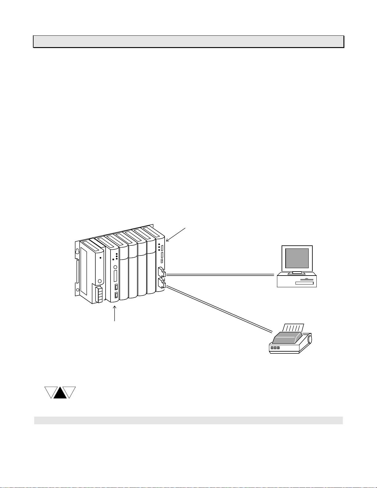
1. AS311 Overview
1.1 Introduction
The ASCI I interface module AS311 (hereaf ter called AS311) is a general purpose data
communicat ion m odule for Toshiba’s Program mable Controller PROSEC-T3 (hereafter
called T3) . By using t he AS311, T3 can communicate with external devices, such as a
micro comput er, bar code reader, printer, display device, sensor, etc., through the
serial inter face RS-232C or RS-422.
The AS311 has t wo ports of the serial interface. One port (channel 1) can be selected
either RS- 232C or RS-422 by switch setting. The other port ( c hannel 2) is RS- 232C
interface. These two ports can be used independently for data receiving and
transmitting.
The t r ansm ission is asynchronous (st ar t - s t op system) .
ASCII is used as t he transmission data code.
The figure below shows the typical system configuration.
NOTE
T3
CPU module
The maximum number of AS311 that can be cont rolled by one T3 is not limited by
software. However, this module consumes maximum 1 A of int ernal 5 Vdc power.
Confirm that the tot al 5 Vdc consum ed current per one power supply module is
within the limit (7 A).
AS311
Channel 1
RS-232C or RS-422
Channel 2
RS-232C
ASCII Interface Module (AS311)
8
Page 11
1. AS311 Overview
1.2 AS311 functions
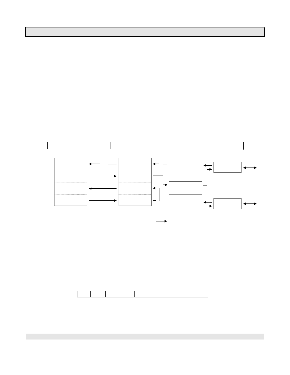
From t he point of view of T3, the AS311 works as communications driver. The
f ollowings are the simplified explanations for T 3 and AS311 functions.
When a message (one set of transmission characters) is received by AS311, the flag
which indicates the receiving complete will come ON. T3 can check the flag status then
read the m essage from the AS311 by using the READ instr u ct ion.
In case of transmitting a message (one set of transmission characters) from T3 through
AS311, T 3 writes t he message into the AS311 by using the WRITE instruction, then
sets the flag which instruct the AS311 to start t r ansm it t ing the message.
T3 AS311
Register Buffer memory
READ Receiving
area Receiving Channel 1
WRITE Transmitting buffer
area
READ Receiving Transmitting
area buffer
WRITE Transmitting
area Receiving Channel 2
buffer
Transmitting
buffer
Here, a m essage (one set of transmission charact er s) means a string of ASCII
character s which is ended by specified trailing code. The default set t ing of the trailing
code is CR (carr iage return code = H0D).
Applicable messag e format (default trailing code):
1 2 3 4 N-1 N
CR
N: message length = 896 bytes max.
In other words, t he AS311 cannot be used for the data communication in which the
transm ission m essage is ended by two or more types of trailing code.
User’s Manual
9
Page 12
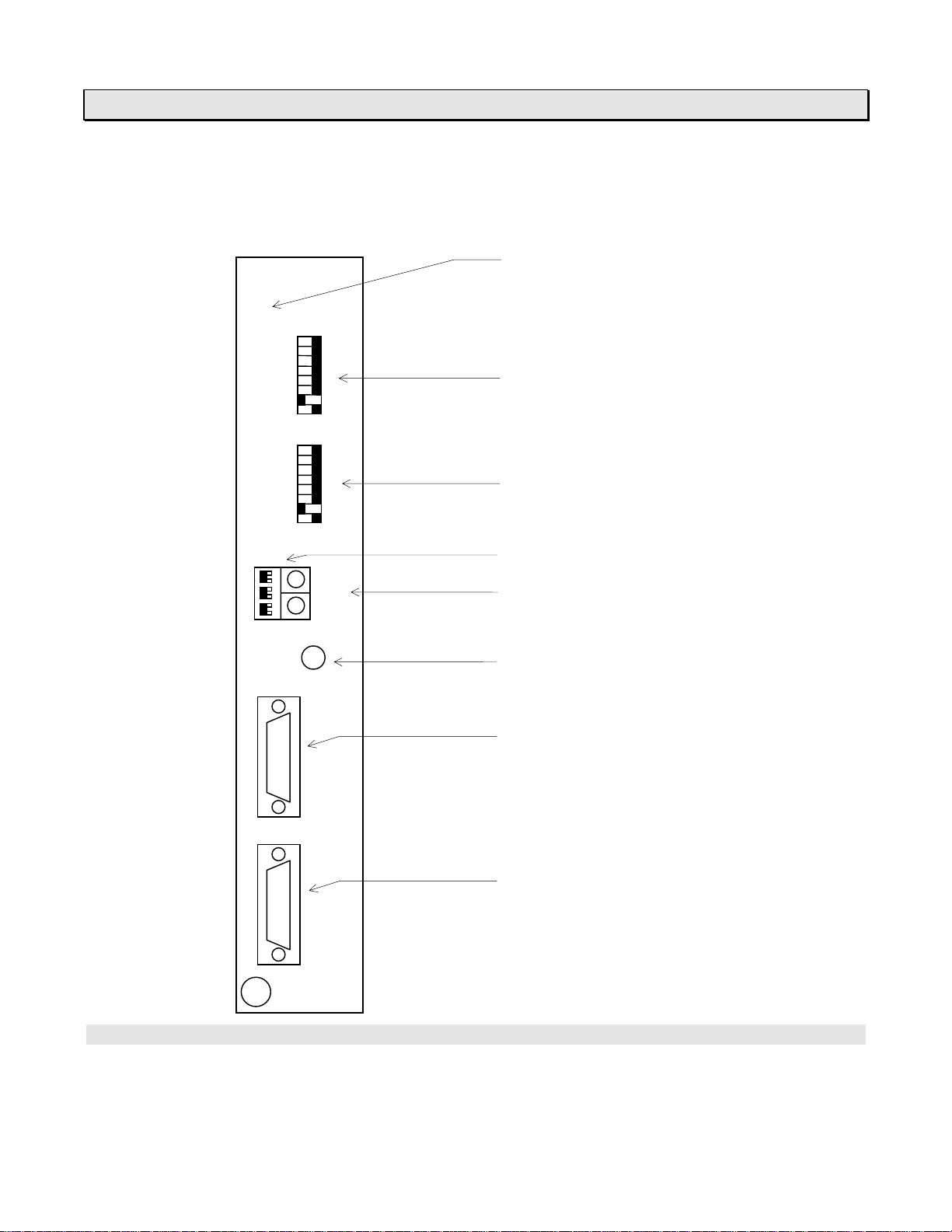
1. AS311 Overview
↓
RSW
RSW
1.3 External features
AS311
•
RUN
•
TX1
•
RX1
•
TX2
•
RX2
ON
SW3
1
2
3
RESET
ON
→
→
SW1
SW2
→
1
2
CH1
CH2
Status LEDs
8
7
6
5
4
3
2
1
Channel 1 transmission parameter
setting switches
8
7
6
5
4
3
2
1
Channel 2 transmission parameter
setting switches
RS-232C/RS-422 selection switches
Optional rotary switches
Hardware reset switch
Channel 1 serial port (RS-232C/RS-422)
D-Sub 25-pin female connector
Channel 2 serial port (RS-232C)
D-Sub 25-pin female connector
ASCII Interface Module (AS311)
10
Page 13
Status LEDs
RUN: Lit when AS311 is operating nor mally
TX 1: Lit while transmit ting data from channel 1
RX1: Lit while receiving data to channel 1
TX 2: Lit while transmit ting data from channel 2
RX2: Lit while receiving data to channel 2
SW1 channel 1 transmission parameter setting switches
8
7
6
5
4
3
2
1
→
ON
No.8 … No use (set always ON)
No.7
OFF ON
Stop bit 2 bit 1 bit
No.6
OFF ON
Data bit length 7 bit 8 bit
No.5
No.4
OFF ON ON
OFF/ON OFF ON
Parity None Even Odd
SW1
1. AS311 Overview
No.3
No.2
No.1
OFF OFF OFF OFF ON ON ON
OFF OFF ON ON OFF OFF ON
OFF ON OFF ON OFF ON OFF
Baud rate 300 600 1200 2400 4800 9600 19200
SW2 channel 2 transmission parameter setting switches
Used to set t he transmission parameters for channel 2. The functions of each switch
are the sam e as the SW1. Set t he transmission parameters independently for
channel 1 and channel 2.
NOTE
The factory settings of the SW1 and SW2 are as shown above figure.
That is, 1 stop bit, 8 data bits, odd parity and 9600 bps.
User’s Manual
11
Page 14
1. AS311 Overview
SW3 RS-232C/RS-422 selection switches (for channel 1)
1
2
3
→
ON
SW3
NOTE
The switches No.2 and No.3 should be set to ON when the AS311
is configured as terminal st at ion on the RS-422 transmission line.
The factory settings of the SW 3 ar e all OFF.
RSW1/RSW2 Optional rotary switches
RSW1
C
80
RSW2
4
C
80
4
Used to select the interface of the channel 1 either
RS-232C or RS-422.
No.1
OFF ON
Interface RS-232C RS-422
Used to connect the terminating resist or ( 120 Ω)
between RXDA and RXDB. (Eff e ct ive for RS-422)
No.2
OFF ON
Terminating Not connect Connect
Used to connect the terminating resist or ( 120 Ω)
between CTSA and CTSB. (Effective for RS-422)
No.3
OFF ON
Terminating Not connect Connect
Always set the RSW1 to 4 and the RSW2 to 0.
(Other settings are f or future use)
Do not set other than above, otherwise the AS311
will not work correctly.
ASCII Interface Module (AS311)
12
Page 15
1. AS311 Overview
Hardware reset switch
When this switch is pressed, the AS311 will be reset. Use t his switch when you
have changed the switch settings.
Channel 1 and channel 2 seri al ports
Used to connect the serial transmission line (RS-232C or RS-422). D- Sub 25-pin
f em ale connectors are provided on the AS311.
The pin assignment is as follows.
Channel 1 Channel 2
(RS-232C/RS-422) (RS-232C)
1 FG
2 TXD
3 RXD
4 RTS
5 CTS
6 6 DSR
7 SG
8 8
9 5 Vdc
10 TXDA
11 RXDA
12 RTSA
13 CTSA
14 14
15 15
16 16
17 17
18 18
19 19
20 DTR
21 TXDB
22 RXDB
23 RTSB
24 CTSB
25 25
• The arrow on the above figure shows the signal direction.
• FG is connected with the T3’s frame g r ound internally. (both channels)
• DTR and RTS are ON while power is on.
• Data transmitting is available when CTS is ON. DSR has no effect for t r ansm ission.
• Pin 9 (5 Vdc) can be used to supply 5 Vdc power. (total max. 50 mA)
↔
→
← for RS-232C
→
←
↔
→
→
← for RS-422
→
←
→ for RS232C
→
← for RS-422
→
←
1 FG
2 TXD
3 RXD
4 RTS
5 CTS
7 SG
9 5 Vdc
10
11
12
13
20 DTR
21
22
23
24
↔
→
←
→
←
←
↔
→
→
User’s Manual
13
Page 16

ASCII Interface Module (AS311)
14
Page 17

Section 2
Specifications
2.1 General specifications
2.2 Functional specifications
2.3 Transmission specifications
User’s Manual
15
Page 18

2. Specifications
2.1 General specifications
Item Specifications Remarks
Power voltage 5 Vdc (supplied from back plane bus)
Current consumption 1.0 A (5 Vdc) maximum Note (1)
Environmental conditions Conforms to T3 specifications
Insulation resistance
Withstand voltage 500 Vac - 1 minute Note (2)
Size T3 I/O module size (1 slot)
Weight 500 g
Note (1) The T3’s power supply module can supply maximum 7 A of internal 5 Vdc.
Check that the internal 5 Vdc current consum ption per one power supply
module does not exceed the limit.
Note (2) Between interface connector pins and internal circuit.
10 MΩ (500 Vdc)
2.2 Functional specifications
Item Specifications
Module type Serial communication interface
I/O allocation type iX+Y 4W
Buffer memory capacity 448 words x 4
(accessed from T3 by READ/WRITE instruction)
Transmission interface 2 channels;
Channel 1 … RS-232C or RS-422 (selectable)
Channel 2 … RS-232C
Display Status LEDs;
RUN … lit when operating normally
TX1 … lit while transmitting data from channel 1
RX1 … lit while receiving data to channel 1
TX2 … lit while transmitting data from channel 2
RX2 … lit while receiving data to channel 2
Connectable devices Computer, bar code reader, display device, sensor,
printer, or other serial ASCII device
RAS function Self diagnosis, watch dog timer ( 200 ms),
transmission error check, etc.
Note (2)
ASCII Interface Module (AS311)
16
Page 19

2. Specifications
2.3 Transmission specifications
Item Channel 1 Channel 2
Interface RS-232C or RS-422 RS-232C
Transmission mode Full-duplex
Synchronizing St art-stop method (asynchronous)
Transmission speed 300, 600, 1200, 2400, 4800, 9600, 19200 bps
Frame format Start bit
Data
Parity
Stop bit
Transmission code ASCII
Message length Max. 896 bytes
Configuration One to one (Note)
Transmission distance Max. 15 m (RS-232C)
Max. 1 km (RS-422)
Connector D-sub 25-pin female D-sub 25-pin female
Note) In case of RS- 422 interface, multiple devices can be connected to one AS311
if the connected RS-422 devices work as slave stations and support multi-point
connection. That is, the connected RS-422 devices must have the tr ansm ission
generators which support the passive state. Also, the RS- 422 devices must
support the message form at which contains the select ing address. In this case,
the number of the connected RS-422 devices is limit ed up t o 10.
On the other hand, the AS311’s transmission g enerator does not support the
passive state. Therefore the AS311 m ust be t he master station in the one-to-N
configuration.
1 bit
7 or 8 bits
even / odd / none
1 or 2 bits
Max. 15 m
User’s Manual
17
Page 20

ASCII Interface Module (AS311)
18
Page 21

Section 3
Cable Connections
3.1 RS-232C connection
3.2 RS-422 connection
User’s Manual
19
Page 22

3. Cable Connections
3.1 RS-232C connection
The following figure shows the RS-232C connection.
AS311 Shielded cable RS-232C device
FG
1
TXD
2
RXD
3
RTS
4
CTS
5
(DSR)
6
SG
7
DTR
20
(1) DSR is suppor ted only on the channel 2.
(2) Connect SG each other.
(3) Use shielded cable. The cable shield should be connected to FG at one end.
(4) I t is recommended to use twisted cable for noise imm unity.
NOTE
Do not connect or remove the connector while the AS311 is powered. Otherwise, it
will cause damage to the AS311.
RXD
TXD
DTR
SG
DSR
RTS
CTS
ASCII Interface Module (AS311)
20
Page 23

3. Cable Connections
3.2 RS-422 connection
The channel 1 can be select ed eit her RS-232C or RS-422. The following figure shows
the RS-422 connect ion.
AS311 Shielded cable RS-422 device
FG
1
10
21
11
22
7
12
23
13
24
TXDA
TXDB
RXDA
RXDB
SG
RTSA
RTSB
CTSA
CTSB
FG
RXDA
RXDB
TXDA
TXDB
SG
CTSA
CTSB
RTSA
RTSB
R
R
(1) O n the AS311, connect the built-in terminating resistors (120 Ω) between RXDA
and RXDB and bet ween CTSA and CTSB by setting switches.
(Set t he SW3-2 and SW3-3 to ON)
(2) O n the RS-422 device, connect the terminating resist ors R (120 Ω - 1/2 W)
between RXDA and RXDB and between CTSA and CTSB.
(3) Connect SG each other.
(4) Use shielded t wisted-pair cable. The A (+) and B (-) of the same signal should be
paired.
(5) The cable shield should be connected to FG at one end.
NOTE
Do not connect or remove the connector while the AS311 is powered. Otherwise, it
will cause damage to the AS311.
User’s Manual
21
Page 24

ASCII Interface Module (AS311)
22
Page 25

Section 4
Register Configuration
4.1 I/O allocation and I/O registers
4.2 AS311 buffer memory
User’s Manual
23
Page 26

4. Register Configuration
4.1 I/O allocation and I/O registers
The AS311 has the I/O type ‘
allocation is perf ormed with mounting the AS311, the f ollowing I/O allocation table will
be created in t he T3.
(T - PDS scr een example - in t he case that AS311 is mounted on Slot 0 of Unit 0)
i X+Y 4W
’ for I/O allocation. When the automatic I/O
Then, 4 I/O registers, XW(n), XW(n+1), YW(n+2) and YW(n+3), are assigned to the
AS311.
In the above example, X W000, XW001, YW002 and YW003 are assigned.
Note that the I/O type has ‘i’ designation. It means that t he T3 will not update the
assigned I/O registers in the batch I/O processing. To read or write data through
the I/O registers, the Direct I/O instruction (FUN235) or the direct I/O designation
(I/IW and O/OW instead of X/XW and Y/YW) is necessary.
The r eason of that is because the reading and writing timings are important f or
handshaking between T3 and AS311. Refer to section 5.
ASCII Interface Module (AS311)
24
Page 27

4. Register Configuration
The following table shows the functions of I/O registers assigned to the AS311.
XW(n) CH1 status
XW(n+1) CH2 status
YW(n+2) CH1 command
YW(n+3) CH2 command
Register Bit Name Description
F Write ready 1: ready to write data (transmit) for channel 1
E Transmit complete 1: transmitting has been completed normally
D Transmit error 1: transmitting has been canceled by error
XW(n) C - 8 − No use (always 0)
(CH1) 7 Read ready 1: ready to read the received data
6 Receive complete 1: receiving for channel 1 has been completed
5 Receive error 1: receiving error has occurred
4 - 0 − No use (always 0)
F Write ready 1: ready to write data (transmit) for channel 2
E Transmit complete 1: transmitting has been completed normally
D Transmit error 1: transmitting has been canceled by error
XW(n+1) C - 8 − No use (always 0)
(CH2) 7 Read ready 1: ready to read the received data
6 Receive complete 1: receiving for channel 2 has been completed
5 Receive error 1: receiving error has occurred
4 - 0 − No use (always 0)
F T ransmit start Set to 1 to start transmitting data fr om channel 1
YW(n+2) E - 8 − No use (set to 0)
(CH1) 7 Read star t Set to 1 to start reading data for channel 1
6 - 0 − No use (set to 0)
F T ransmit start Set to 1 to start transmitting data fr om channel 2
YW(n+3) E - 8 − No use (set to 0)
(CH2) 7 Read star t Set to 1 to start reading data for channel 2
6 - 0 − No use (set to 0)
NOTE
F E D C B A 9 8 7 6 5 4 3 2 1 0
No use No use
No use No use
No use No use
No use No use
These bits are used for handshak ing between T3 and AS311. The detailed
function and timing are explained in section 5.
User’s Manual
25
Page 28

4. Register Configuration
4.2 AS311 buffer memory
As explained in the previous section, the I/O registers that are assigned to AS311
are used to cont rol the reading and writing timings ( handshake) between T3 and
AS311.
On the ot her hand, for exchanging the transmission data between T3 and AS311, the
AS311’s buf fer memory is used.
This sect ion explains the buffer memory contents and how to access the buffer
memory.
4.2.1 Memory map
The AS311 has t he buffer memory that is used to exchange data with T3. The overall
map of the buffer me m or y is as follows.
Address W ord data
0 Stat us and com mand 4 words - same data as I/O registers
4 Parameter
128 Channel 1
reading (receiving)
data area
576 Channel 1
writing (transmitting )
data area
1024 Channel 2
reading (receiving)
data area
1472 Channel 2
writing (transmitting )
data area
1920 Access inhibited
124 words - transmission parameters, etc.
448 words
448 words
448 words
448 words
128 words
ASCII Interface Module (AS311)
26
Page 29

4. Register Configuration
4.2.2 Buffer memory access
T3 can r ead t he AS311’s buffer memory contents by using READ inst ruction (FUN237).
Also, T 3 can write dat a into the buffer me m or y by using WRITE instruction (FUN238).
READ instruction (FUN237)
Expression:
[ (A) READ (B) → (C) ]
Operands:
(A): I/O register (XW/YW) assigned to the AS311
(B): Starting address of the buffer memory to be read
(B)+1: Number of words to be read (max. 256)
(C): Starting register of the destination
Example:
R0100
[ 00128 MOV D5000 ] [ 00064 MOV D5001 ]
[ X W000 READ D5000 → D1000 ]
When R0100 is ON, 64 words of buffer memory data star t ing with address 128
are read from the AS311 which is allocated to XW000. And the dat a ar e st ored
in D1000 and after.
User’s Manual
27
Page 30

4. Register Configuration
WRI TE inst ruct i on (FUN238)
Expression:
[ (A) WRITE (B) → (C) ]
Operands:
(A): Starting register of the source
(B): Starting address of the buffer memory to be written
(B)+1: Number of words to be written (max. 256)
(C): I/O register (XW/YW) assigned to the AS311
Example:
R0101
[ 00576 MOV D5000 ] [ 00100 MOV D5001 ]
[ D2000 WRITE D5000 → YW002 ]
When R0101 is ON, 100 words of data starting with D2000 (D2000 to D2099)
are written into the buffer memory address 576 and after of the AS311 which is
allocated to YW 002.
ASCII Interface Module (AS311)
28
Page 31

4. Register Configuration
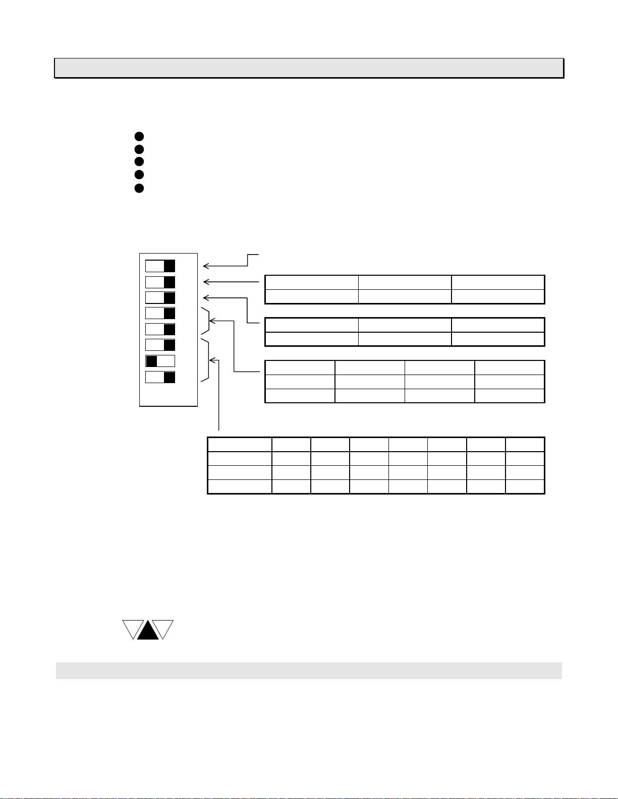
4.2.3 Parameter area
The par am et er area of the buff er m em or y contains t he following contents.
Address Address
0 CH1 status 64
1 CH2 status Status and 65
2 CH1 command command 66
3 CH2 command 67
4 Status 1 68
5 RSW1/2 information 69
6 SW1 information 70
7 SW2 information 71 Reserved
8 CH1, CH2 72
9 common 73
10 parameters 74
11 75
12 Command 1 76
13 77
14 78
15 79
16 CH1 receive error 80 CH2 receive error
17 CH1 transmit error 81 CH2 transmit error
18 CH1 channel status 82 CH2 channel status
19 CH1 receive length 83 CH2 receive length
20 84
21 85
22 86
23 87
24 CH1 trailing code 88 CH2 trailing code
25 CH1 time-out check CH1 89 CH2 time-out check CH2
26 parameters 90 parameters
27 91
28 92
29 93
30 94
31 95
63 127
Note: Blanks are for fut ur e use. ( Reser ved)
User’s Manual
29
Page 32

4. Register Configuration
Status and command (0 - 3)
The addresses 0 to 3 store the same data as the I/O registers that are assigned to the
AS311.
Refer to section 4.1 f or details.
0 CH1 stat us = XW( n)
1 CH2 stat us = XW( n+1)
2 CH1 comm and = YW ( n+2)
3 CH2 comm and = YW ( n+3)
Status 1 (4)
The address 4 shows the AS311 module status. If an er r or has occurred in the AS311,
the error code is stored here.
F E D C B A 9 8 7 6 5 4 3 2 1 0
RDY ERR 0 0 0 0 0 0 Error code
4
Bit F RDY (Ready) 1 = operating normally
Bit E ERR (Error) 1 = error state
Bit 7-0 Er r o r code Shows the detected error item if ERR is 1.
RSW1/2 information (5)
The address 5 stores the rotary switches RSW1 and RSW 2 setting status.
F E D C B A 9 8 7 6 5 4 3 2 1 0
0 0 0 0 0 0 0 0 RSW1 RSW2
5
Bit 7-4 RSW1 Stores the rotary switch 1 (RSW1) setting status.
Bit 3-0 RSW2 Stores the rotary switch 2 (RSW2) setting status.
0 = under initialization or error state
0 = no error (normal)
(H00 when normal)
See section 6.2.1 for details.
0 - F
0 - F
ASCII Interface Module (AS311)
30
Page 33

SW1 information (6)
The address 6 stores the setting status of the channel 1 transmission parameter set ting
switches (SW1).
6
OFF ON
ON: 1 OFF: 0
SW2 information (7)
The address 7 stores the setting status of the channel 2 transmission parameter set ting
switches (SW2).
7
OFF ON
ON: 1 OFF: 0
4. Register Configuration
F E D C B A 9 8 7 6 5 4 3 2 1 0
0 0 0 0 0 0 0 0 SW1
SW1
8
7
6
5
4
3
2
1
F E D C B A 9 8 7 6 5 4 3 2 1 0
0 0 0 0 0 0 0 0 SW2
SW2
8
7
6
5
4
3
2
1
User’s Manual
31
Page 34

4. Register Configuration
Command 1 (12)
The address 12 is used to reset the AS311 by T3 progr am .
Two types of reset commands are available, hot reset and cold r eset .
The hot reset is used to change the tr ailing code and the time-out check time set t ings.
The cold reset is used to initialize the AS311. The t r ailing code and the time-out check
time will be reset to the default sett ing . The operation of the cold reset is the same as the
hard reset switch and power on initialization.
Refer to sections 5.5, 5.6 and 5. 7 for these functions.
F E D C B A 9 8 7 6 5 4 3 2 1 0
RST 0 0 0 0 0 0 0 Command number
12
Bit F RST (Reset) 1 = reset request
Bit 7-0 Com mand
number
CH1 receive error (16) and
CH2 receive error (80)
The address 16 (for channel 1) and the addr ess 80 ( for channel 2) indicate the error
contents if an error has been detect ed in r eceiving a message. This inform at ion is set
during the received message read sequence.
Refer to section 6.2.3 for details.
16 or 80
F E D C B A 9 8 7 6 5 4 3 2 1 0
0 0 0 0 BRK PE FE OE Receive error code
Bit B BRK ( Br eak) 1 = break detected
Bit A PE ( Par ity error) 1 = parity error
Bit 9 FE
(Framing error)
Bit 8 OE
(Overrun error)
Bit 7-0 Receive err or
code
0 = normal (no reset request)
HFE = hot reset
HFF = cold reset
0 = normal
0 = normal
1 = framing error
0 = normal
1 = overrun error
0 = normal
Shows the error code regarding received message.
(H00 when normal)
See section 6.2.3 for details.
ASCII Interface Module (AS311)
32
Page 35

CH1 transmit error (17) and
CH2 transmit error (81)
The address 17 (for channel 1) and the addr ess 81 ( for channel 2) indicate the error
contents if an error has occurred dur ing message transmitting . This information is set
during the write sequence for m essage transmitting.
Refer to section 6.2.4 for details.
17 or 81
CH1 channel status (18) and
CH2 channel status (82)
The address 18 (for channel 1) and the addr ess 82 ( for channel 2) indicate the control
signal status. This inf or m ation is always updated.
18 or 82
Note: (1) The channel 1 does not support DSR. Therefore, bit 7 of the address 18 is
always 0.
( 2) The bit 2 is always 1.
F E D C B A 9 8 7 6 5 4 3 2 1 0
0 0 0 0 0 0 0 0 Transmit error code
Bit 7-0 Transmit error
code
F E D C B A 9 8 7 6 5 4 3 2 1 0
0 0 0 0 0 0 0 IDL DSR 0 0 0 CTS 1 0 0
Bit 8 IDL (Idle) 1 = transmitter is idle state
Bit 7 DSR
(Data set ready)
Bit 3 CTS
(Clear to send)
4. Register Configuration
Shows the error code for transmitting.
(H00 when normal)
See section 6.2.4 for details.
0 = transmitter is non-idle state
1 = DSR is ON
0 = DSR is OFF Note (1)
1 = CTS is ON
0 = CTS is OFF
User’s Manual
33
Page 36

4. Register Configuration
CH1 receive length (19) and
CH2 receive length (83)
The address 19 (for channel 1) and the addr ess 83 ( for channel 2) indicate the length of
the received message (number of bytes) . This information is set during the received
message read sequence.
19 or 83
CH1 trailing code (24) and
CH2 trailing code (88)
The address 24 (for channel 1) and the addr ess 88 ( for channel 2) store the trailing
codes. The default setting is H0D (CR code).
To change the trailing code, write the desired code into this address then write the hot
reset command into the Command 1 (12). See section 5.6 for this procedure.
24 or 88
F E D C B A 9 8 7 6 5 4 3 2 1 0
Bit F-0 Received
message length
F E D C B A 9 8 7 6 5 4 3 2 1 0
0 0 0 0 0 0 0 0 Trailing code
Bit 7-0 Trailing code Stores the trailing code.
Received message length
Shows the received message length (bytes).
0 - 896
Initial value at power on is H0D (carriage retur n ) .
ASCII Interface Module (AS311)
34
Page 37

CH1 time-out check (25) and
CH2 time-out check (89)
The address 25 (for channel 1) and the addr ess 89 ( for channel 2) store the time-out
check times. If the t im e bet ween each receiving charact er exceeds the specified time-out
check time, it becomes the receiving t im e- out error. The default set t ing is 1 second.
To change the setting, write t he desir ed data into this address then write the hot reset
command into the Command 1 (12). See sect ion 5. 7 for this procedure.
25 or 89
F E D C B A 9 8 7 6 5 4 3 2 1 0
Bit F-0 Time-out check
time
4. Register Configuration
Time-out check time
Stores the time-out check tim e ( 0. 1 s units).
Valid data range is 1 to 600 (0.1 to 60 s). If 0 or more
than 600 is specified, the time-out check will not work.
Initial value at power on is 10 (1 s).
User’s Manual
35
Page 38

4. Register Configuration
4.2.4 Receiving and transmitting data area
The r eceiving and transmitting data area is provided to exchange the com m unication
character s between T3 and AS311. The address ranges in the AS311 buf fer memory
are as follows.
Address W ord data
128 Channel 1
reading (receiving)
data area
576 Channel 1
writing (transmitting )
data area
1024 Channel 2
reading (receiving)
data area
1472 Channel 2
writing (transmitting )
data area
When AS311 receives a message (one set of transmission characters), AS311 set s the
character s into the receiving data area starting with the address 128 or 1024. Then T3
can read these char acters from the receiving dat a ar ea by using READ inst r uction.
When T3 attempts to send a message via AS311, T3 writes the characters into the
transm it t ing data area starting with the address 576 or 1472 by using WRITE
instruct ion, and instructs AS311 to start transmit t ing. AS311 recognizes from the
character st or ed in the starting address (576 or 1472) to t he t railing code character as
the one set of transmitting message.
Ref er t o section 5 for message receiving/t r ansmitting procedure.
448 words
448 words
448 words
448 words
ASCII Interface Module (AS311)
36
Page 39

Section 5
Operation Procedure
5.1 Transmission message format
5.2 Received message read sequence
5.3 Write sequence for message tr ansm it t ing
5.4 Checking the AS311 operation status
5.5 Resetting the AS311 by software
5.6 Setting the trailing code
5.7 Setting the time-out check time
User’s Manual
37
Page 40

5. Operation Procedure
5.1 Transmission message format
The t r ansm ission m essage is composed by ASCII characters and a specified t r ailing
code. T he default setting of t he trailing code is CR (carriage ret urn code = H0D).
Ref er to section 5.6 for setting the trailing code other than CR.
The m aximum length of a message is 896 bytes. An example of t he m essage is
shown below.
1 2 3 4 5 6 7 8 9
″0″ ″1″ ″2″ ″A″ ″B″ ″7″ ″8″ ″9″
In the above figure, ″x″ means an ASCII character. For example, ″0″ is H30.
When the above message is received or transm it t ed, the data arrangements in the
T3 r egisters are as follows.
Register F 8 7 0
n
n+1
n+2
n+3
n+4 CR
″1″ ″0″
″A″ ″2″
″7″ ″B″
″9″ ″8″
Transmission message
CR
″0″
″1″
″2″
″A″
″B″
″7″
″8″
″9″
CR
ASCII Interface Module (AS311)
38
Page 41

5. Operation Procedure
5.2 Received message read sequence
5.2.1 Flag control timing
In case of receiving a message, the f ollowing flags are used for handshaking between
T3 and AS311. These flags are the bits of the I/O registers assigned to the AS311.
Ref er t o section 4.1.
Read ready
Receive complete
Receive error
Read start
The m essage receiving procedure is as follows. It is called “received message read
sequence”.
AS311 receives a message
AS311 sets Receive complete to ON
T3 sets Read st art to ON
Normal receiving Receiving error
AS311 sets the message int o buffer AS311 sets the error information into
memory (receiving data area), and buffer memory (parameter area)
sets the received message length into
buffer memory (parameter area)
AS311 sets Read ready to ON, and AS311 sets Receive error to ON, and
resets Receive complete to OFF resets Receive complet e to OFF
T3 reads the message for m buffer T3 r eads t he er r or information from
memory (receiving data area) buffer memory (parameter area)
by READ instruction by READ instruction
T3 resets Read start to OFF T3 resets Read start to OFF
AS311 resets Read ready to OFF AS311 resets Receive error to OFF
Bit 7 of XW(n) for channel 1 or XW(n+1) for channel 2
Bit 6 of XW(n) for channel 1 or XW(n+1) for channel 2
Bit 5 of XW(n) for channel 1 or XW(n+1) for channel 2
Bit 7 of YW(n+2) for channel 1 or YW(n+3) f or channel 2
User’s Manual
39
Page 42

5. Operation Procedure
5.2.2 T3 sample program for message receiving
A sample program for the “received messag e read sequence” is shown below.
This sam ple pr ogram is for the channel 1 of the AS311 that is allocated to XW000 YW003.
(Main program)
Operation for normal received message
Operation for receiving error
(Subrout ine No. 0)
ASCII Interface Module (AS311)
40
Page 43

5. Operation Procedure
In this sam ple program, the following devices/registers are used.
R0100 AS311 status (ON when ready) - Refer to section 5.4
R0200 Receiving normal complete (comes ON when receiving is complete normally)
R0300 Receiving error complete (comes ON when receiving error has occurred)
X0006 Receive complete flag
X0007 Read ready flag
X0005 Receive error flag
Y0027 Read st ar t flag
D0000 - D0063 Received message is stored here
D3000 Receiving error information is st or ed here
D4000 - D4001 Parameters for READ instruction
This sam ple pr ogram works as follows.
Main program
- Rung 1: Calls Subroutine No. 0 when the AS311 is normal and both R0200 and
R0300 are OFF.
- Rung 2: When R0200 comes ON (normal receiving), perform s t he necessary
operation for the received message, then resets R0200 to OFF.
- Rung 3: When R0300 comes ON (r eceiving er r or has occurred), performs t he error
processing , t hen resets R0300 to OFF.
Subroutine No. 0
- Rung 1: Indicates the entry of Subroutine No. 0.
- Rung 2: Reads XW000 and XW001 from the AS311 by direct I/O instruction.
- Rung 3: Sets Y0027 (Read start flag) t o O N if X0006 (Receive complete flag) is O N.
- Rung 4: When X0007 (Read ready flag) comes ON, reads the received message from
the AS311’s buffer memory, 64 words starting with address 128, by READ instr uct ion,
and stores it into D0000 and after. Then reset s Y0027 (Read start flag) to O FF, and
sets R0200 t o O N.
When X0005 (Receive error flag) comes ON, reads the error information from t he
AS311’s buf fer memory, 1 word of address 16, by READ instr uct ion, and stores it into
D3000. T hen r eset s Y0027 ( Read st ar t flag) to OFF, and sets R0300 t o O N.
- Rung 5: Writes YW002 and YW003 into the AS311 by direct I/O instruction.
- Rung 6: Indicates the return of Subr out ine No. 0.
User’s Manual
41
Page 44

5. Operation Procedure
Explanation f or this sample program:
(1) The “ r eceived message read sequence” is programm ed on Subr out ine No. 0.
(2) The Subr outine No. 0 is called from Main program with reset t ing R0200 and R0300
to OFF.
(3) When a message is received norm ally, R0200 will come ON and t he m essage
(ASCII characters) will be stored in D0000 to D0063. In t his sample program, the
received message length information (buffer memory address 19) is not used. The
maximum length of a message is 128 bytes (64 words) because the number of
read words of the READ instruction is programm ed as 64 words.
(4) When an error has occurr ed in r eceiving t he m e ssage, R0300 will come ON and
the error information will be stored in D3000. For details of the error information,
refer to section 6.2.3.
ASCII Interface Module (AS311)
42
Page 45

5. Operation Procedure
5.3 Write sequence for message transmitting
5.3.1 Flag control timing
In case of transmitting a message, t he following flags are used for handshaking
between T3 and AS311. These flags are the bits of the I/O registers assigned to the
AS311. Refer to section 4.1.
Write ready
Transmit complete Bit E of XW(n) for channel 1 or XW(n+1) for channel 2
Transmit error
Transmit start
The m essage transmitting procedure is as follows. It is called “write sequence for
message transmitting”.
T3 checks Write ready is ON
T3 writes a message into buffer
memory (transmitting data ar ea)
by WRITE instruction
T3 sets Transmit start to ON
AS311 resets Write ready to OFF
Normal transmitting Transmitting error
AS311 sends out the message and AS311 sets the err or information into
sets Transmit complete to ON buffer memory (parameter area) and
sets Transmit error to ON
T3 resets Transmit st art to OFF
T3 reads the error information from
buffer memory (parameter area)
AS311 resets Transmit compl ete to by READ instruction, and resets
AS311 resets Transmit error to OFF,
and sets Write ready to ON
OFF, and sets Write ready to ON Transmit start to OFF
Bit F of XW(n) for channel 1 or XW(n+1) for channel 2
Bit D of XW(n) for channel 1 or XW(n+1) for channel 2
Bit F of YW(n+2) for channel 1 or YW(n+3) f or channel 2
User’s Manual
43
Page 46

5. Operation Procedure
5.3.2 T3 sample program for message transmitting
A sample program for the “write sequence for message transmitt ing” is shown below.
This sam ple pr ogram is for the channel 1 of the AS311 that is allocated to XW000 YW003.
(Main program)
Set the transmission message into
D0200 - D0263, and set R0110 to ON
Operation for transmitt ing error
(Subrout ine No. 1)
ASCII Interface Module (AS311)
44
Page 47

5. Operation Procedure
In this sam ple program, the following devices/registers are used.
R0100 AS311 status (ON when ready) - Refer to section 5.4
R0110 Internal flag to star t transmitting
R0201 Transmitting normal complete (comes ON when transmitting is complete
normally)
R0301 Transmitting error com plet e ( comes ON when transmitting error has
occurred)
X000F Write r eady flag
X000E Transmit complete f lag
X000D Transmit er r or flag
Y002F Transmit start flag
D0200 - D0263 Transmitting message is set here
D3010 Transmitting error information is stored here
D4010 - D4011 Parameters for W RI TE instruction
D4000 - D4001 Parameters for READ instruction
This sam ple pr ogram works as follows.
Main program
- Rung 1: Pr epares a transmission message and sets it into D0200 and after (maximum
64 words in this sample). Then sets R0110 to ON.
- Rung 2: Calls Subroutine No. 1 when the AS311 is normal and R0110 is ON.
- Rung 3: When R0201 comes ON (normal transmitting), r esets R0110 and R0201 to
OFF.
- Rung 4: When R0301 comes ON (t r ansm it t ing error has occurred), performs the error
processing , then resets R0110 and R0301 to OFF.
Subroutine No. 1
- Rung 1: Indicates the entry of Subroutine No. 1.
- Rung 2: Reads XW000 and XW001 from the AS311 by direct I/O instruction.
- Rung 3: When X000F (Write ready flag) is ON, writes the message that is st ored in
D0200 to D0263 into t he AS311’s buffer memory, 64 words start ing with address 576,
by WRITE instruction, and sets Y002F (Transmit start flag) to ON.
- Rung 4: When X000E (Transmit complete flag) com es O N, r eset s Y002F ( Transmit
start flag) to OFF, and sets R0201 t o O N.
When X000D (Transmit error flag) comes ON, reads the error information from the
AS311’s buf fer memory, 1 word of address 17, by READ instr uct ion, and stores it into
D3010. T hen r eset s Y002F ( Transmit start flag ) to OFF, and sets R0301 to ON.
- Rung 5: Writes YW002 and YW003 into the AS311 by direct I/O instruction.
- Rung 6: Indicates the return of Subr out ine No. 1.
User’s Manual
45
Page 48

5. Operation Procedure
Explanation f or this sample program:
(1) The “ write seq uence for message transmitt ing ” is programmed on Subroutine
No. 1.
(2) To st ar t transmitting, set the m essage (ASCII characters) into D0200 and after.
Then set R0110 to ON.
The message length is maximum 128 bytes (64 words) in this sample program.
(3) When R0110 is set to ON while the AS311 is ready, the Subroutine No. 1 will be
called and the message transmitting will be started.
(4) When the message is transmitted normally, R0201 will come ON. Then R0110 will
be reset to OFF.
(5) When an error has occurr ed in t r ansm it ting the message, R0301 will come ON and
the error information will be stored in D3010. For details of the error information,
refer to section 6.2.4.
ASCII Interface Module (AS311)
46
Page 49

5. Operation Procedure
5.4 Checking the AS311 operation status
AS311 operation st atus information is stored in the AS311’s buffer memory address 4
(Stat us 1) . T3 can read this informat ion by using READ inst ruction.
A sample program is shown below. This sample program is f or the AS311 that is
allocated to XW000 - YW003.
The above sample program works as follows.
- Rung 1: Reset s S0051 ( I nstruction error flag) t o O FF, and sets parameters for the
READ instruction.
- Rung 2: Reads the operation status information from the AS311’s buffer memory
address 4 (Stat us 1) .
- Rung 3: When S0051 (Inst r uction error flag) is OFF and R050F ( Ready) is ON, turns
R0100 to ON.
It means that the AS311 is operating norm ally when R0100 is ON.
If R050E (Error) is ON, the AS311 is in err or state. In that case, the err or code is
stored in t he lower 8 bits of RW 050. For the error code, refer t o section 6.2.1.
If S0051 (Instruction error flag) is ON, it means that an er r or has occur r ed dur ing the
READ instruction execution.
User’s Manual
47
Page 50

5. Operation Procedure
5.5 Resetting the AS311 by software
AS311 can be reset by T3 pr ogram. Two types of resetting are available, cold reset
and hot reset .
The cold r eset is used t o r eset the AS311 error state. When the cold reset is executed,
the AS311 will be initialized. The t railing code and the time-out check t im e ar e also
reset t o t he default settings. This function is the same as pressing the hardware reset
switch and power on initialization.
On the ot her hand, the hot reset is used to change the trailing code and/or the time-out
check time.
For executing these functions, write the following data into the AS311’s buffer mem ory
address 12 (Comm and 1) . The data writing into this address must be one-shot.
Clod reset: H80FF
Hot reset: H80FE
The writt en dat a will be cleared to 0 by AS311 when the operation is com pleted.
A sample program for the cold reset is shown below. This sample program is for the
AS311 that is allocated to XW000 - YW003.
In this sample program, the cold reset operation will be started by setting R0120 to ON.
(Main program)
(Subrout ine No. 2)
(H80FF)
For the hot r eset, refer to sections 5.6 and 5. 7.
ASCII Interface Module (AS311)
48
Page 51

5. Operation Procedure
5.6 Setting the trailing code
The default setting of the trailing code is CR (carriage return code = H0D). The tr ailing
code can be changed by T3 pr ogram.
To do t his, write desired trailing code into the AS311’s buffer memory address 24 (CH1
trailing code) and/or address 88 (CH2 trailing code), and execute the hot reset (ref er to
section 5.5).
A sample program is shown below. This sample program is f or the AS311 that is
allocated to XW000 - YW003.
In this sample program, the trailing code changing routine will be executed once when
the AS311 stat us is changed to ready (R0100 comes ON - refer to section 5.4), and the
channel 1 trailing code will be changed to H03.
If the channel 2 trailing code and/or the t im e- out check time are also changed, write
these data on the Main program Rung 2 before calling Subr outine No. 3 in the same
manner.
(Main program)
(Subrout ine No. 3)
(H0003)
(H80FE)
User’s Manual
49
Page 52

5. Operation Procedure
5.7 Setting the time-out check time
The default setting of the time-out check time is 1 second. The t ime- out check time
can be changed by T3 pr ogram. The valid setting rang e is 0. 1 to 60.0 seconds in 0.1
second units. Refer to section 4.2.3.
To change the time-out check time, write desired value into the AS311’s buffer mem or y
address 25 (CH1 t ime-out check) and/or address 89 (CH2 time-out check), and
execute the hot r eset ( r efer to section 5.5).
T3 pr ogram for this purpose is almost sam e as that for setting t he t r ailing code (refer to
section 5.6) . Only the difference is writing t he time-out check time instead of the trailing
code. See Rung 2 of the following sample. In this sam ple, the channel 1 time-out check
time is chang ed t o 5 seconds.
If the channel 2 time-out check time and/or the trailing code are also changed, write
these data on the Main program Rung 2 before calling Subr outine No. 3 in the same
manner.
(Main program)
ASCII Interface Module (AS311)
50
Page 53

Section 6
RAS Information
6.1 LED indication
6.2 Buffer memory information
6.3 Trouble shooting
User’s Manual
51
Page 54

6. RAS Information
6.1 LED indication
On the AS311, five status LEDs are provided as follows. These LEDs are useful to
check t he AS311 oper ation status and the communication status.
RUN
TX1
RX1
TX2
RX2
RUN Indicates the AS311 operation status.
Lit when the AS311 is in ready state.
Not lit when the AS311 is in error or under initialization.
TX1 Indicates the channel 1 communication status.
Lit while some data is transmitting f rom the AS311.
RX1 Indicates the channel 1 communication stat us.
Lit while some data is receiving into the AS311.
TX2 Indicates the channel 2 communication status.
Lit while some data is transmitting f rom the AS311.
RX2 Indicates the channel 2 communication stat us.
Lit while some data is receiving into the AS311.
ASCII Interface Module (AS311)
52
Page 55

6. RAS Information
6.2 Buffer memory information
Various RAS information are stored in the AS311’s buffer memory. These information
can be read by READ instruct ion. When some abnormality has occurred, check these
information.
6.2.1 Module status
Address 4 of the buffer mem or y stores the AS311 module status.
F E D C B A 9 8 7 6 5 4 3 2 1 0
RDY ERR 0 0 0 0 0 0 Error code
4
Bit F RDY (Ready) 1 = operating normally
0 = under initialization or error state
Bit E ERR (Error) 1 = error state
0 = no error (normal)
Bit 7-0 Er r o r code Shows the detected error item if ERR is 1.
See the table below (H00 when normal)
Error
code
H01 CPU error CPU err or has been detected
H02 ROM error ROM error has been detected
H03 RAM error Work RAM error has been
H04 Buffer memory
H05 Switch setting
H10 Watchdog
H11 Trap interrupt
H12 Buffer memory
Type of error Description Status
Operation is stopped.
during initialization.
Operation is stopped.
during initialization.
Operation is stopped.
detected during initialization.
error
abnormal
timer error
error
time-out error
Buffer memory error has been
detected during initialization.
Switch setting abnormality has
been detected during
initialization.
Watchdog timer error has
occurred during operation.
Trap interrupt has occurred by
detecting illegal instruction
during operation.
Buffer memory time-out has
occurred during operation.
Operation is stopped.
Operation is stopped.
Operation is stopped.
Cold reset will be
effective.
Operation is stopped.
Cold reset will be
effective.
Operation is stopped.
Cold reset will be
effective.
User’s Manual
53
Page 56

6. RAS Information
6.2.2 Switch setting status
Addresses 5, 6 and 7 of the buffer m em or y store the switches setting status. Check
that the information agrees with the physical setting status if some abnormality has
occurred.
F E D C B A 9 8 7 6 5 4 3 2 1 0
0 0 0 0 0 0 0 0 RSW1 RSW2
5
Bit 7-4 RSW1 Stores the rotary switch 1 (RSW1) setting status.
0 - F
Bit 3-0 RSW2 Stores the rotary switch 2 (RSW2) setting status.
0 - F
F E D C B A 9 8 7 6 5 4 3 2 1 0
0 0 0 0 0 0 0 0 SW1
6
OFF ON
ON: 1 OFF: 0
F E D C B A 9 8 7 6 5 4 3 2 1 0
0 0 0 0 0 0 0 0 SW2
7
OFF ON
ON: 1 OFF: 0
SW1
8
7
6
5
4
3
2
1
SW2
8
7
6
5
4
3
2
1
ASCII Interface Module (AS311)
54
Page 57

6. RAS Information
6.2.3 Error information for data receiving
Address 16 for channel 1 and address 80 for channel 2 store the er r or information for
data receiving .
16 or 80
F E D C B A 9 8 7 6 5 4 3 2 1 0
0 0 0 0 BRK PE FE OE Receive error code
Bit B BRK ( Br eak) 1 = break detected
0 = normal
When break has been detected, receive buffer is
cleared. The next message can be received.
Bit A PE ( Par ity error) 1 = parity error
0 = normal
When parity err or has occur r ed, the message is
disabled. The next message can be received.
Bit 9 FE
(Framing error)
Bit 8 OE
(Overrun error)
Bit 7-0 Receive err or
code
Error
code
H01 Receive time-
H02 Message
H03 Receive buffer
Type of error Description Stat us
out error
length error
overflow
1 = framing error
0 = normal
When f r aming error has occurred, the message is
disabled. The next message can be received.
1 = overrun error
0 = normal
When overrun error has occur red, the message is
disabled. The next message can be received.
Shows the error code regarding received message.
See the table below. (H00 when normal)
Specified time-out check
time has elapsed between
characters.
The message length has
exceeded the limit. (896
bytes)
Receive buffer overflow
has occurred.
The rest of the message
will be received as the next.
The message is disabled.
The next message can be
received.
The message is disabled.
The next message can be
received.
User’s Manual
55
Page 58

6. RAS Information
6.2.4 Error i n formation for data transmitting
Address 17 for channel 1 and address 81 for channel 2 store the er r or information for
data transmitting.
17 or 81
F E D C B A 9 8 7 6 5 4 3 2 1 0
0 0 0 0 0 0 0 0 Transmit error code
Bit 7-0 Transmit error
code
Error
code
H01 Trailing code
Type of error Description Stat us
missing
Shows the error code for transmitting.
See the table below. (H00 when normal)
The trailing code has not
been written into the
buffer memory.
The message is disabled.
The next message can be
transmitted.
ASCII Interface Module (AS311)
56
Page 59

6. RAS Information
6.3 Trouble shooting
When AS311 does not work properly, check the following points.
W hen AS311’s RUN Does t he PO WER LED on If no, check the power
LED does not light; the T3 power supply module voltage/connection.
light ?
If no, check the inter nal
5 Vdc current
consumption.
Is the AS311 mounted Remove the AS311,
securely on the base ? and mount again
securely.
When RX1/RX2 LED Are the transmission Check the cable
does not light while signals (RXD, SG, etc.) connection.
the connected device is connected properly ?
transmitting a message;
When the received data Does the receive error Check t he transmission
cannot be read pr oper ly; occur ? parameters (baudrate,
parity, etc.).
Check the cable
connection.
Confirm the receive
error information.
I s t he T3 program working Check the T 3 pr ogram.
correctly ?
When a data cannot be Does the t r ansm it er ror Confirm the transmit
transmitted from the occur ? error information.
AS311 (TX1/TX2 LED
does not light); Check the T3 program.
Is the CTS signal Check the cable
connected properly ? connection.
If CTS signal is OFF,
data transmitting
is prohibited.
User’s Manual
57
Page 60

ASCII Interface Module (AS311)
58
Page 61

Appendix
A.1 Specification of the READ instruction
A.2 Specification of the WRITE inst r uction
User’s Manual
59
Page 62

Appendix
A.1 Specification of the READ instruction
FUN 237 Special module data read (READ)
Reads designated range of data from the special module.
Input Execution output
[ A READ B → C ]
Function
• This instruction reads data f r om the buffer memor y of the special module that is
designated by operand A, and stores them in T3’s r egisters starting with operand C.
• The transfer source address (buffer memory
address) is designated by operand B.
• The transfer size (number of words) is
designated by operand B+1.
Operand
Device
Opr Name
Input Action Output ERF
OFF No execution OFF
ON Normal execution ON
Error (see Note 2) ON ON
X Y S L R Z T. C. I O XW YW SW LW RW W T C D F IW OW I J K
Register
Constant
Index
A Special
module
B Transfer
parameter
C Top register
of destination
√ √
√ √ √ √ √ √ √ √ √ √
√ √ √ √ √ √ √ √ √
Program example
R0000
[ XW000 READ RW010 → D0100 ]
• When R0000 is ON, t he buffer memory data of the size indicated by RW011, starting with the
address indicated by RW010 of the special module allocated to XW000, are read and stored in
D0100 and after.
• The maximum number of words to be read is 256 words.
X W000 special module T3
RW010 20
Buf fer memory RW011 16
20 1234 READ D0100 1234
35 5678 16 words D0115 5678
√ √
√
ASCII Interface Module (AS311)
60
Page 63

Appendix
Note 1) The special module can be designated not only by the assigned register , but
also by the mounting position. The mount ing position is designated by a
constant data for the operand A as follows.
(Unit number) × 256 + (Slot number)
H
Slot number (hexadecimal)
Unit number (hexadecimal)
For example, if a special module is mounted on Slot- 4, Unit-0 (basic unit)
and allocated to XW008 - YW 011, the following two READ instructions
function the same.
[ XW008 READ RW010 → D0100 ]
[ H0004 READ RW010 → D0100 ]
Note 2) The READ instruction is not executed as error in the following cases. In
these cases, ERF (instruction error f lag = S0051) is set to ON.
Unit number Hexadecimal
0 H00
1 H01
2 H02
3 H03
• When the operand A is other than a valid constant (see Note 1) or XW/YW
register.
• When the designated special module has been disconnected.
• When no answer error occur s with the desig nated special module.
• When the number of words transferred exceeds 256 words.
• When the source table of transfer is out of the valid range.
• When the dest ination table of transfer is out of the valid range.
Slot number Hexadecimal
0 H00
1 H01
2 H02
3 H03
4 H04
5 H05
6 H06
7 H07
8 H08
9 H09
10 H0A
User’s Manual
61
Page 64

Appendix
A.2 Specification of the WRITE instruction
FUN 238 Special module data write (WRITE)
Writ es designated range of data into t he special m odule.
Input Execution output
[ A WRITE B → C ]
Function
• This instruction transfer s dat a st or ed in T3’s registers starting with operand A int o t he buffer
memory of the special module that is designated by operand C.
• The destination address (buffer memory
address) is designated by operand B.
• The transfer size (number of words) is
designated by operand B+1.
Operand
Device
Opr Name
Input Action Output ERF
OFF No execution OFF
ON Normal execution ON
Error (see Note 2) ON ON
X Y S L R Z T. C. I O XW YW SW LW RW W T C D F IW OW I J K
Register
Constant
Index
A Top register
of source
B Transfer
parameter
C Special
module
√ √ √ √ √ √ √ √ √ √
√ √ √ √ √ √ √ √ √ √
√ √
Program example
R0000
[ D0100 WRI TE RW010 → YW002 ]
• When R0000 is ON, t he register data of the size indicated by RW011, starting with D0100,
are transferred to the buffer memory start ing with the address indicated by RW010 of the
special module allocated to YW002.
• The maximum number of words to be transferred is 256 words.
T3 YW002 special module
RW010 320
RW011 150 Buffer mem o r y
D0100 1234 WRIT E 320 1234
D0249 5678 150 words 469 5678
√
√ √
ASCII Interface Module (AS311)
62
Page 65

Appendix
Note 1) The special module can be designated not only by the assigned register , but
also by the mounting position. The mount ing position is designated by a
constant data for the operand C as follows.
(Unit number) × 256 + (Slot number)
H
Slot number (hexadecimal)
Unit number (hexadecimal)
For example, if a special module is mounted on Slot- 2, Unit-1 (expansion
unit #1) and allocated to XW020 - YW023, the following two WRITE
instructions function the same.
[ D0100 WRITE RW010 → XW020 ]
[ D0100 WRITE RW010 → H0102 ]
Note 2) The WRITE instruction is not executed as error in the following cases. In
these cases, ERF (instruction error flag = S0051) is set t o O N.
Unit number Hexadecimal
0 H00
1 H01
2 H02
3 H03
• When the oper and C is ot her than a valid constant (see Note 1) or XW/YW
register.
• When the designated special module has been disconnected.
• When no answer error occur s with the desig nated special module.
• When the number of words transferred exceeds 256 words.
• When the source table of transfer is out of the valid range.
• When the dest ination table of transfer is out of the valid range.
Slot number Hexadecimal
0 H00
1 H01
2 H02
3 H03
4 H04
5 H05
6 H06
7 H07
8 H08
9 H09
10 H0A
User’s Manual
63
Page 66

TOSHIBA CORPORATION
Industrial Equipment Department
1-1, Shibaura 1-chome, Minato-ku
Tokyo 105-8001, JAPAN
Tel: 03-3457-4900 Fax: 03-5444-9268
 Loading...