

Page 1

SERVICE MANUAL
(*1), as indicated by the underlined serial number.
Page
1
of
1
02.04.2015
file://C:\Program Files\zeus\js\!!fcover.html
LCD Color Television
19AV605PG
Ver. 2.00
This model is classified as a green product
This Service Manual describes replacement parts for the green product. When repairing this
green product, use the part(s) described in this manual and
For (*1) and (*2), refer to
SOLDER
© TOSHIBA CORPORATION
.
GREEN PRODUCT PROCUREMENT and LEAD-FREE
lead-free solder (*2).
Page 2
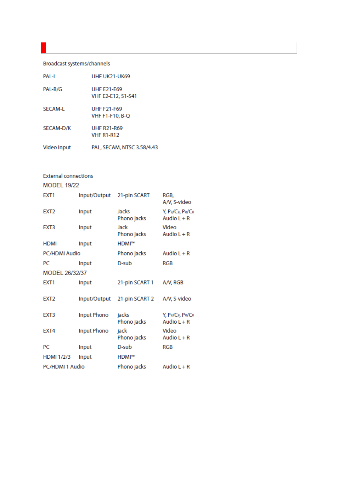
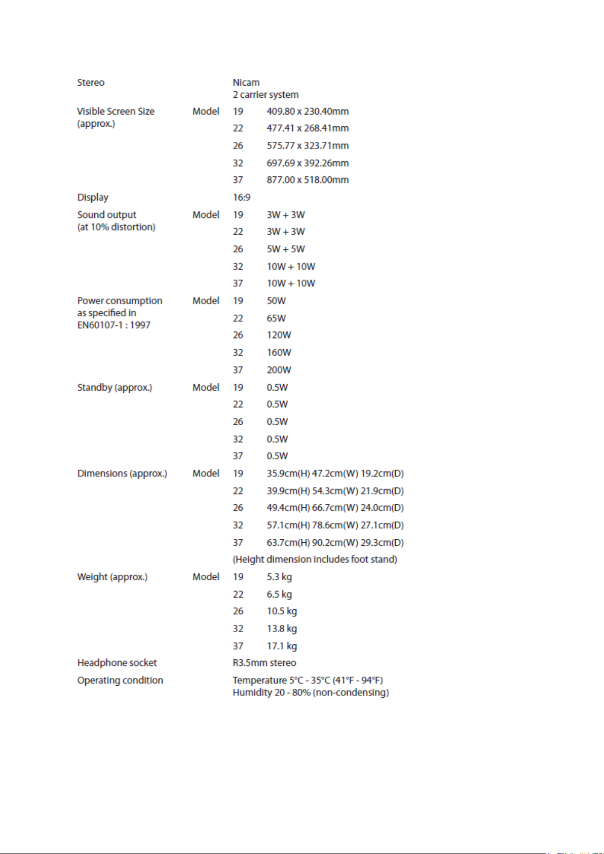
SPECIFICATION
Page
1
of
2
02.04.2015
file://C:\Documents and Settings\Admin\
Рабочий стол
\19AV605PG Ver. 2.00\html\!
...
Page 3
Page
2
of
2
02.04.2015
file://C:\Documents and Settings\Admin\
Рабочий стол
\
19AV605PG Ver. 2.00\html\!
...
Page 4

IMPORTANT NOTICE
Page
1
of 1WARNING
02.04.2015
file://C:\Program Files\zeus\js\!!warning.html
WARNING:
You are requested that you shall not modify or alter the information or data
provided herein without prior written consent by Toshiba. Toshiba shall not
be liable to anybody for any damages, losses, expenses or costs, if any,
incurred in connection with or as a result of such modification or alteration.
THE INFORMATION OR DATA HEREIN SHALL BE PROVIDED "AS IS"
WITHOUT ANY WARRANTY OF ANY KIND, EITHER EXPRESS OR IMPLIED
WARRANTY OF MERCHANTABILITY AND FITNESS FOR A PARTICULAR
PURPOSE.
Toshiba shall not be liable for any damages, losses, expenses or costs, if
any, incurred in connection with or as a result of use of any information or
data provided herein.
Page 5

IMPORTANT NOTICE
is necessary to view drawings and to activate the functions of this system. Please
up windows are limited by
the enhanced security function and this system may not work. In that case, perform the Internet Explorer
Page
1
of 9User's Guide
02.04.2015
file://C:\Program Files\zeus\js\!!uguide(e).html
User's Guide
Contents:
Install Autodesk DWF Viewer
Internet Explorer Settings
Operating Environment
Functions Provided on Each Drawing Page
Using with Network
Install Autodesk DWF Viewer
Autodesk DWF Viewer
download and install.
Internet Explorer Settings
When Windows XP SP2 or Windows Vista is used, ActiveX control and pop-
setting using the following procedure to restore normal operation.
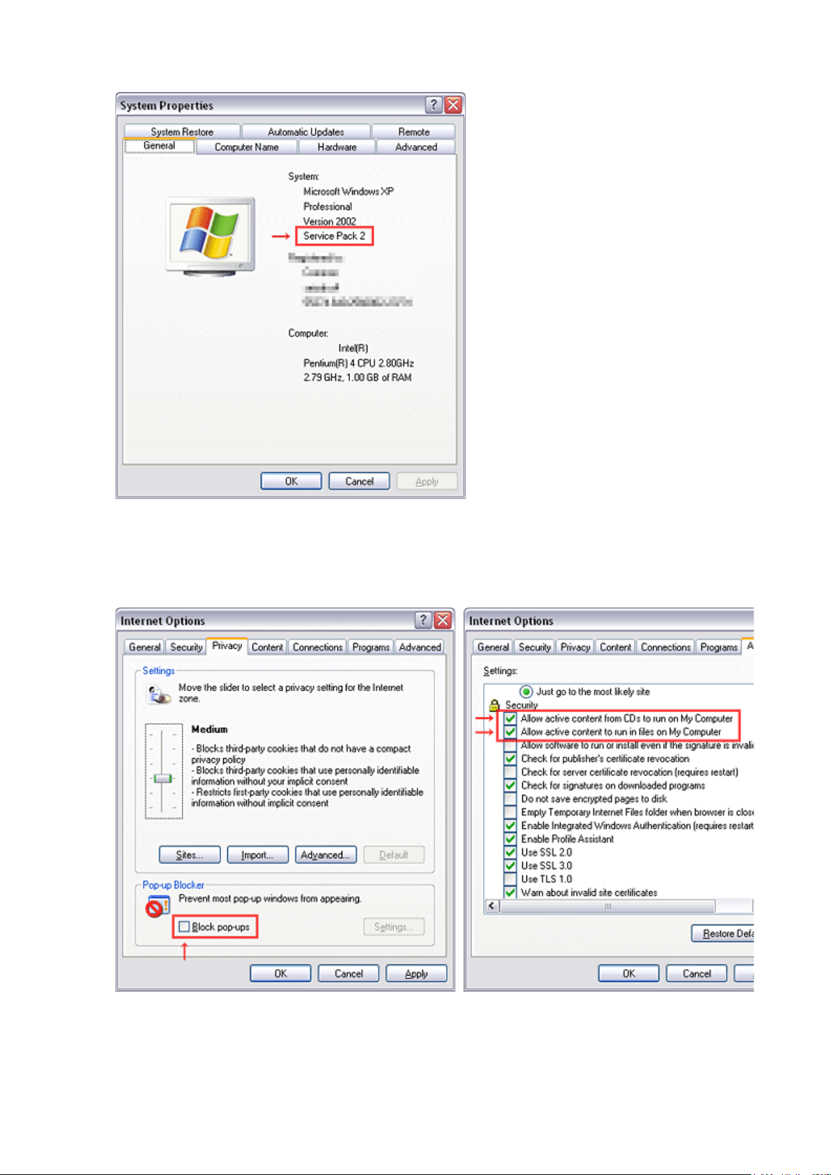
1. Windows version check
[My Computer (right-click)] - [Properties]
Page 6
Page
2
of 9User's Guide
02.04.2015
file://C:\Program Files\zeus\js\!!uguide(e).html
2. Internet Explorer setting
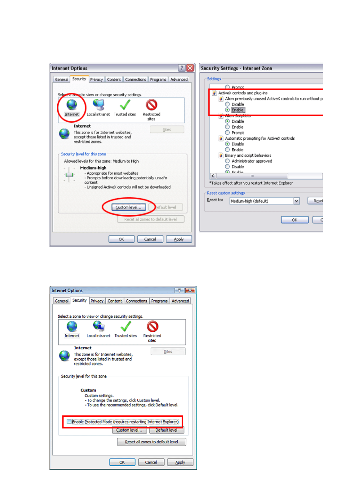
[Tools] - [Internet Options]
for Internet Explorer 7
Page 7
Page
3
of 9User's Guide
02.04.2015
file://C:\Program Files\zeus\js\!!uguide(e).html
for Windows Vista
Page 8

When the character string of a part on the drawing is clicked, its information is popped up at the location.
You can get any parts information immediately on the screen without referring to the maintenance parts list.
You can search any part within the displayed drawing or within the whole schematic diagram/board view by
up window displayed by clicking a part 's character string allows to
When a name at the end of a signal line in a divided schematic diagram is clicked, the destination of the
signal is searched and the display changes to the destination. Connecter destinations can also be searched in
When two or more search results are provided, their drawing names are displayed, allowing you to choose a
Page
4
of 9User's Guide
02.04.2015
file://C:\Program Files\zeus\js\!!uguide(e).html
Operating Environment
PC : Pentium III or higher recommended
Monitor : 1024 x 768 or higher resolution recommended
Mouse : A mouse with wheel recommended
OS : Microsoft Windows 2000 SP4 / XP / Vista
Browser :
Drawing viewer : Autodesk DWF Viewer 6.0 / 7.0
* Use the software following respective license terms and conditions.
Microsoft Internet Explorer 6.0 / 7.0
Functions Provided on Each Drawing Page
Parts Information Reference Function
Parts Search Function
specifying a location number. The popsearch the part within the applicable schematic diagram, board view or spare parts list.
A circle appears when the part is found, showing the part's location within the drawing.
Signal Line/Connector Destination Display Function
the same way.
desired drawing to display.
Page 9

Layer Display Changing Function
When any of the color buttons on the toolbar is clicked, it can be selected to display desired layer in its color
or not to display each layer. This allows you to see the pattern layer only by setting other layers to "non
When a pattern on a board view is clicked, it is highlighted in green. This allows easy pattern tracing.
The Autodesk DWF Viewer enables to print the displayed drawing region as it is on a printer. It also allows
path names written on the source files of each
Create the appropriate folder where the ZEUS Engine Program Ver.2 and the ZEUS Service Manual
Page
5
of 9User's Guide
02.04.2015
file://C:\Program Files\zeus\js\!!uguide(e).html
display".
PC Board View Pattern Highlighting Function
Specified Area Printing Function
to print a large-sized drawing in multiple pieces (tile printing).
Using with Network
PRECAUTION
To use ZEUS Service Manual Ver.2 with network, the file-
ZEUS Engine Program Ver.2 and ZEUS Service Manual Ver.2 are to be modified.
Perform the procedure described below.
Preparation
1. Run the program file zuesFPch.exe to install the program file for File-Path to the Local PC.
-> Download zeusFPch_setup.zip (2.3MB)
2. Run the program file ZeusSetup_v2.0.exe to install the ZEUS Engine Program in C:\Program
Files\zeus of the local PC. This can be done by running the installer program provided.
3.
Ver.2 to be stored in the server.
Page 10
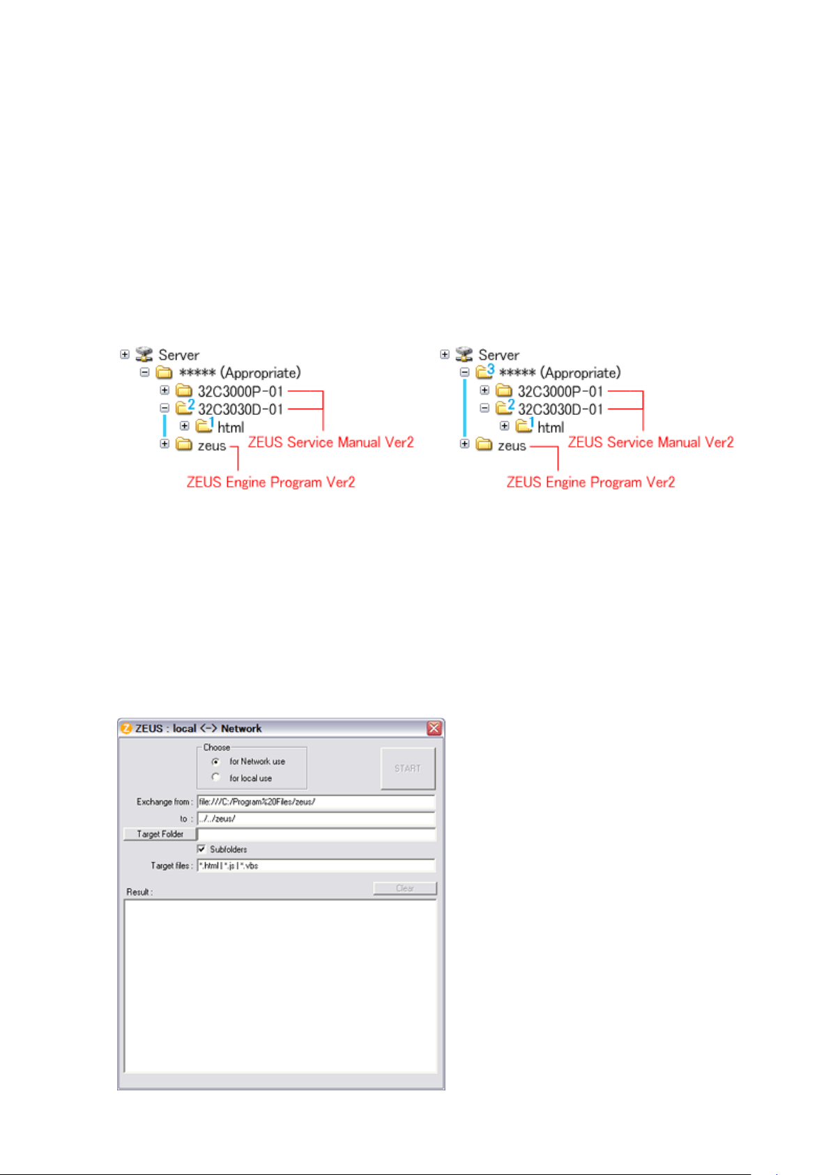
4. Move the ZEUS Engine Program of step 2 to the folder created at step 3 in the Server.
path names written in both source files of ZEUS
Page
6
of 9User's Guide
02.04.2015
file://C:\Program Files\zeus\js\!!uguide(e).html
5. Detach the ZEUS Service Manual Ver.2 to the folder created at step 3 in the Server.
6. Unzip the ZEUS Service Manual Ver.2 within the folder in the Server.
Example of folder
Procedure of File-Path
The zeusFPch is the exclusive program to exchange the file-
Manual and ZEUS Engine program into those applicable to the network use.
Page 11
path of both ZEUS Engine Program and ZEUS Service Manual to use with
network, pay the attention to set the "Exchange to" column that should have a proper relation between
In the "Exchange to" column shows the relation between ZEUS Service Manual and ZEUS Engine
Page
7
of 9User's Guide
02.04.2015
file://C:\Program Files\zeus\js\!!uguide(e).html
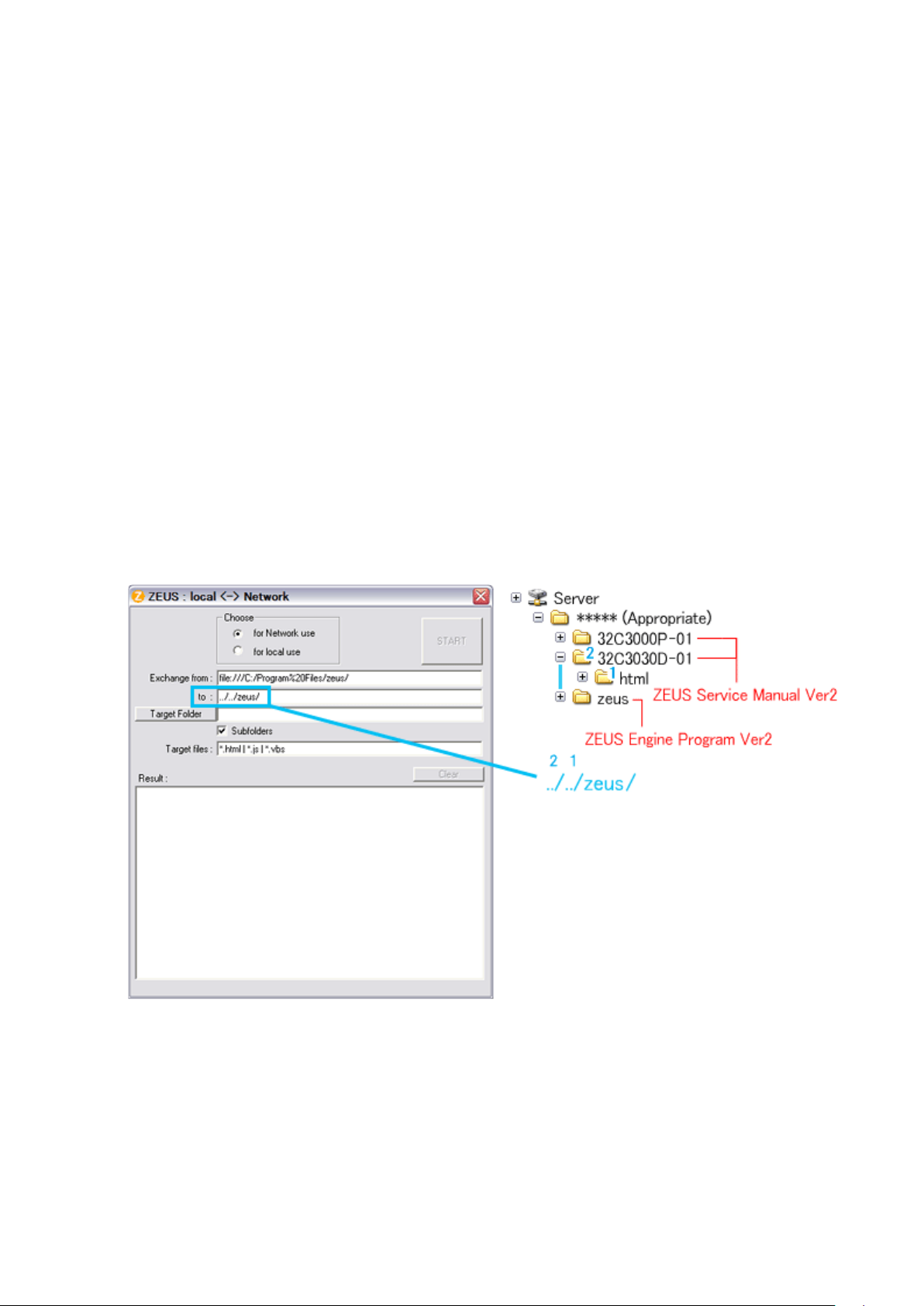
1. Whenever changing the file-
ZEUS Engine Program and ZEUS Service Manual with referring the following.
Run the zeusFPch and set "Exchange to" by referring to the examples below.
Example 1 :
Program.
../ counts the relation between.
Thus in this case, it must be ../../zeus/ (2 counts).
Example 2 :
In this case, it must be ../../../zeus/ (3 counts).
Page 12
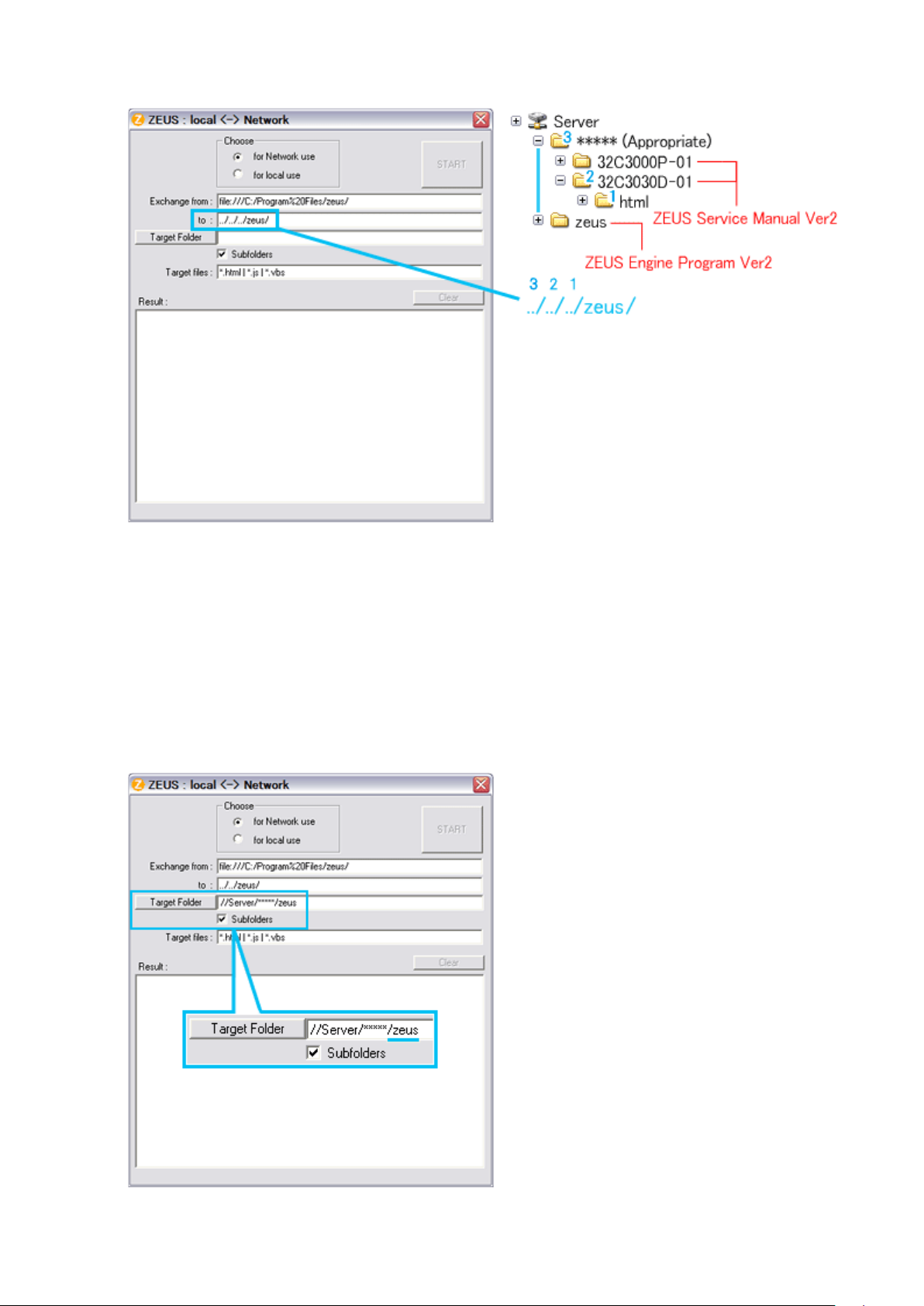
Set ZEUS Engine Program in the created folder in the server to the "Target Folder", and then press
Page
8
of 9User's Guide
02.04.2015
file://C:\Program Files\zeus\js\!!uguide(e).html
2. Run the zeusFPch to change the path in the ZEUS Engine Program Ver.2.
3.
"START".
(This procedure is one time only)
Page 13
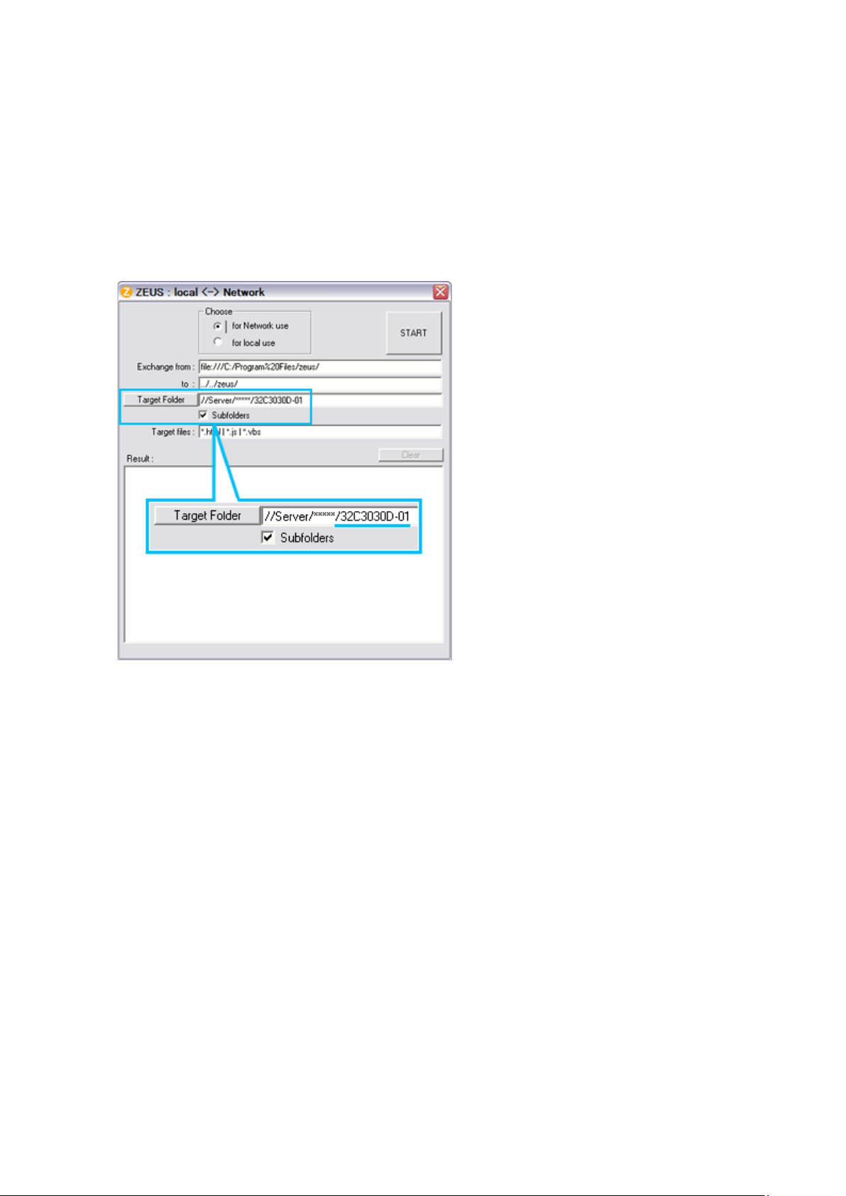
4. Run the ZeusFPch to change the path in the ZEUS Service Manual Ver2.
Set unzipped ZEUS Service Manual in the created folder in the server to the "Target Folder", and then
up window appears at the left
Page
9
of 9User's Guide
02.04.2015
file://C:\Program Files\zeus\js\!!uguide(e).html
5.
press "START".
(This procedure is required whenever placing service manual.)
Confirmation
Confirm that service manual on the server can be operated normally by client PC.
Note:
In case of accessing the ZEUS Manual through WEB site, the small pop-
bottom corner on the screen whenever searching the location links. This is not malfunction.
Page 14

IMPORTANT NOTICE
Through WEB, ver. 6.5 has been released but with it, the linking function in this manual may
Page
1
of 2A Known Malfunction
02.04.2015
file://C:\Program Files\zeus\js\!!malfunction.html
A Known Malfunction
Autodesk® DWF™ Viewer version
(Free software provided through WEB)
Use Autodesk DWF Viewer ver. 6.0.
not work properly.
If ver. 6.5 has been installed, uninstall it and reinstall ver. 6.0.
To get ver. 6.0, click the icon, or contact to the nearest Toshiba Service Centre for further
assistance.
Freezing windows opened
(Cannot close the open windows)
This may happen occasionally.
In case of encountering this, follow the procedure below.
1. Press [Ctrl], [Alt] and [Delete] keys at the same time to engage windows security
windows.
2. Then, choose TASK manager and Application tab, and select TOSHIBA SERVICE
MANUAL-Microsoft Internet Explorer.
3. Click TASK-end.
Main Window back forwarded
The real cause has not been found yet but with this condition, nothing disturbs the service
manual operation.
Page 15

Continue to use by operating the windows.
Page
2
of 2A Known Malfunction
02.04.2015
file://C:\Program Files\zeus\js\!!malfunction.html
Precaution when opening the diagrams
While opening the diagrams, the menu in the left frame changes its color to GRAY. This is
an indication that the viewer is processing.
With this condition, the menu indication color may stick to the GRAY color or Windows
may freeze if clicking other menu.
To avoid such things, do not operate any others while menu turns GRAY color.
If entering this, re-open the service manual or refresh the left frame.
Page 16

GREEN PRODUCT PROCUREMENT
Corporation recognizes environmental protection as a key management tasks, and is doing its
Page
1
of 1GREEN PRODUCT PROCUREMENT
02.04.2015
file://C:\Program Files\zeus\js\!!green.html
The EC is actively promoting the WEEE & RoHS Directives that define standards for
recycling and reuse of Waste Electrical and Electronic Equipment and for the Restriction of
the use of certain Hazardous Substances. From July 1, 2006, the RoHS Directive will
prohibit any marketing of new products containing the restricted substances.
Increasing attention is given to issues related to the global environmental. Toshiba
utmost to enhance and improve the quality and scope of its environmental activities. In line
with this, Toshiba proactively promotes Green Procurement, and seeks to purchase and use
products, parts and materials that have low environmental impacts.
Green procurement of parts is not only confined to manufacture. The same green parts used
in manufacture must also be used as replacement parts.
Page 17

LEAD-FREE SOLDER
free solder must
free solder may result in damage to the component and or PCB being
Page
1
of 1LEAD
-
FREE SOLDER
02.04.2015
file://C:\Program Files\zeus\js\!!l
-
f_solder.html
This product is manufactured using lead-free solder as a part of a movement within the
consumer products industry at large to be environmentally responsible. Lead-
be used in the servicing and repair of this product.
WARNING: This product is manufactured using lead free solder.
DO NOT USE LEAD BASED SOLDER TO REPAIR THIS PRODUCT!
The melting temperature of lead-free solder is higher than that of leaded solder by 86ºF to
104ºF (30ºC to 40ºC). Use of a soldering iron designed for lead-based solders to repair
product made with lead-
soldered. Great care should be made to ensure high-quality soldering when servicing this
product especially when soldering large components, through-hole pins, and on PCBs as the
level of heat required to melt lead-free solder is high.
Page 18
PARTS LIST
Capacitors
OMF
Page
1
of
2
02.04.2015
file://C:\Documents and Settings\Admin\
Рабочий стол
\19AV605PG Ver. 2.00\html\l
...
Precaution
WARNING: BEFORE SERVICING THIS CHASSIS, READ THE "SAFETY
PRECAUTION"
AND "PRODUCT SAFETY NOTICE".
CAUTION: The international hazard symbols " " in the schematic diagram
and the parts list designate components which have special characteristics
important for safety and should be replaced only with types identical to
those in the original circuit or specified in the parts list.
The mounting position of replacements is to be identical with originals.
Before replacing any of these components, read carefully the
PRECAUTION"
and "PRODUCT SAFETY NOTICE".
"SAFETY
Do not degrade the safety of the receiver through improper servicing.
Note:
The part number must be used when ordering parts, in order to assist in processing, be
sure to include the Model number and Description.
The PC board assembly with mark is no longer available after the end of the
production.
Abbreviations
CD : Ceramic Disk
Resistors CF : Carbon film
: Oxide Metal Film
PF : Plastic Film
CC : Carbon Composition
VR : Variable Resistor
EL : Electrolytic
MF : Metal Film
Page 19

FR : Fusible Resistor
Page
2
of
2
02.04.2015
file://C:\Documents and Settings\Admin\
Рабочий стол
\
19AV605PG Ver. 2.00\html\l
...
All CD and PF capacitors are ±5 %, 50 V and all resistor, ±5 %, 1/6 W unless otherwise
noted.
Page 20
PARTS LIST
All Block
Cabinet
E100
75 01 50 71
BEZEL ASSY, 19AV615DB, 705TZ834061
Cabinet
E110
75 01 51 95
BACK COVER ASSY, 19AV605PB, 705TZ834062
Cabinet
E112
75 01 50 70
SCREW, (BC TO FB SCREW TYPE 1), 0Q1T1030
-12-47-
CR3
Cabinet
E114
75 01 51 93
SCREW, (BC TO FB SCREW TYPE 2), 0Q1T
-
330--8-47-CR3
Cabinet
E120
75 01 50 72
BASE ASSY, 19AV615DB, 705TZ834065
Cabinet
E124
75 01 49 51
SCREW, (BASE TO STAND), 0M1T1740
-10-47-
CR3
Cabinet
E130
75 01 50 73
SIDE KEY ASSY, 19AV615DB, 705TZ834068
Cabinet
E140
75 01 51 96
COVER ASSY, SIDE I/O, 19AV605PB, 705TZ834069
Electric Parts
E200
75 01 51 97
PC BOARD ASSY, MAIN, 19AV605PB, CBPFR3HBA1
Electric Parts
E250
75 01 50 77
PC BOARD ASSY, POWER, G3377
-B-X-X-3-
081104, PWTV8941GAAJ
Electric Parts
E260
75 01 50 75
PC BOARD ASSY, KEY, 19AV615DB, KEPF8AB2
Electric Parts
E265
75 01 50 74
PC BOARD ASSY, IR, T2992
-C-X-X-1-
080428, IRPF8AA5
Electric Parts
E300
75 01 39 39
LCD PANEL, LC190WH1
-
TLA1
Electric Parts
E310
75 01 51 92
HARNESS, 30P
-
30P 260MM(LVDS CABLE), 095G801830FA85
Electric Parts
E320
75 01 50 88
POWER CORD, 1500MM NON
-
METAL TIE, 089G404A15NIST
Page
1
of
1
02.04.2015
file://C:\Documents and Settings\Admin\
Рабочий стол
\19AV605PG Ver. 2.00\html\l
...
Block :
Location :
Parts No. :
Block Location Parts No. Description
Search
Search
Page :
1 / 2
Jump
SMM L
Page 21
PARTS LIST
Electric Parts
Electric Parts
E200
75 01 51 97
PC BOARD ASSY, MAIN, 19AV605PB, CBPFR3HBA1
Electric Parts
E250
75 01 50 77
PC BOARD ASSY, POWER, G3377
-B-X-X-3-
081104, PWTV8941GAAJ
Electric Parts
E260
75 01 50 75
PC BOARD ASSY, KEY, 19AV615DB, KEPF8AB2
Electric Parts
E265
75 01 50 74
PC BOARD ASSY, IR, T2992
-C-X-X-1-
080428, IRPF8AA5
Electric Parts
E300
75 01 39 39
LCD PANEL, LC190WH1
-
TLA1
Electric Parts
E310
75 01 51 92
HARNESS, 30P
-
30P 260MM(LVDS CABLE), 095G801830FA85
Electric Parts
E320
75 01 50 88
POWER CORD, 1500MM NON
-
METAL TIE, 089G404A15NIST
Electric Parts
E322
75 01 50 68
AC SOCKET, AND WIRE 100/90MM, 087G501A
--5--
X
Electric Parts
E330
75 01 50 67
SPEAKER, 8 OHM 3.5W 25X80MM, 078G
-
494--4--Y
Electric Parts
E340
75 01 51 91
HARNESS, 11P
-
3P+6P 260/290MM(MAIN TO KEY/IR), 095G801411FA13
Electric Parts
E350
75 01 51 90
HARNESS, 4P
-
2*(2*PAST) 400+450MM(SPEAKER), 095G8014
-
4FA49
Electric Parts
E370
75 01 51 89
HARNESS, 11P(SAN)
-
10P 160MM(POWER TO MAIN), 095G
-
82011X
Page
1
of
1
02.04.2015
file://C:\Documents and Settings\Admin\
Рабочий стол
\19AV605PG Ver. 2.00\html\l
...
Block :
Location :
Parts No. :
Block Location Parts No. Description
Search
Search
Page :
1 / 1
Jump
Jump
SMM L
Page 22

PARTS LIST
Accessory
Accessory
E400
75 01 48 27
REMOCON HAND UNIT, CT
-
90326
Accessory
E410
75 01 51 98
ACCESSORY KIT, (BASE SCREW, USER MANUAL, ETC), 705TZ841065
Page
1
of
1
02.04.2015
file://C:\Documents and Settings\Admin\
Рабочий стол
\19AV605PG Ver. 2.00\html\l
...
Block :
Location :
Parts No. :
Search
Search
Page :
Block Location Parts No. Description
1 / 1
Jump
Jump
SMM L
Page 23
FIRMWARE UPDATING
Page
1
of 3How to update using a USB Mass
-
storage device
02.04.2015
file://C:\Documents and Settings\Admin\
Рабочий стол
\19AV605PG Ver. 2.00\html\!
...
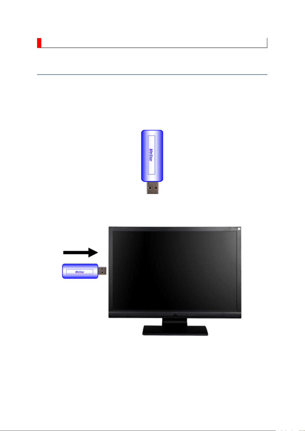
How to update using a USB Mass-storage device
1. Copy the software corresponding to the model to USB Mass-Storage device. (root
directory)
Note: The software should be renamed to upgrade.pkg from the original one before
copying.
Fig.1 USB Mass-storage device
2. Turn TV off, then plug USB Mass-storage device into the USB slot on the TV.
Fig.2 Plugging in USB Mass-storage device into the USB slot on TV
(Viewing from the TV front)
Page 24

Turn TV on, then a software updating wizard will be displayed. Select "YES" and press
Page
2
of 3How to update using a USB Mass
-
storage device
02.04.2015
file://C:\Documents and Settings\Admin\
Рабочий стол
\
19AV605PG Ver. 2.00\html\!
...
Fig.3 Plugging USB Mass-storage device into the USB slot on the TV (Actual view)
3.
"OK" button on the remote control to start the updating.
Fig.4 Updating Wizard
4. Upon completion, the display will show the message.
Fig.5 Updating completion
Page 25

5. Unplug the USB Mass-storage device, and turn TV off.
Page
3
of 3How to update using a USB Mass
-
storage device
02.04.2015
file://C:\Documents and Settings\Admin\
Рабочий стол
\
19AV605PG Ver. 2.00\html\!
...
Fig. 6 Removing USB Mass-storage device
6. Turn TV on and press "MENU" and "0000" on the remote control to confirm a new
software version.
Fig. 7 FW version checking display
Page 26

PARTS LIST
Cabinet
Cabinet
E100
75 01 50 71
BEZEL ASSY, 19AV615DB, 705TZ834061
Cabinet
E110
75 01 51 95
BACK COVER ASSY, 19AV605PB, 705TZ834062
Cabinet
E112
75 01 50 70
SCREW, (BC TO FB SCREW TYPE 1), 0Q1T1030
-12-47-
CR3
Cabinet
E114
75 01 51 93
SCREW, (BC TO FB SCREW TYPE 2), 0Q1T
-
330--8-47-CR3
Cabinet
E120
75 01 50 72
BASE ASSY, 19AV615DB, 705TZ834065
Cabinet
E124
75 01 49 51
SCREW, (BASE TO STAND), 0M1T1740
-10-47-
CR3
Cabinet
E130
75 01 50 73
SIDE KEY ASSY, 19AV615DB, 705TZ834068
Cabinet
E140
75 01 51 96
COVER ASSY, SIDE I/O, 19AV605PB, 705TZ834069
Page
1
of
1
02.04.2015
file://C:\Documents and Settings\Admin\
Рабочий стол
\19AV605PG Ver. 2.00\html\l
...
Block :
Location :
Parts No. :
Block Location Parts No. Description
Search
Search
Page :
1 / 1
Jump
Jump
SMM L
Page 27

PARTS LIST
Packing
Packing
E500
75 01 50 79
CARTON BOX, 19AV615DB, Z44G9022939
-
1A
Packing
E510
75 01 50 78
CUSHION KIT, 19AV615DB, Z44G9006001
Packing
E520
75 01 50 76
PE BAG, (SET)(520*740), 19AV615DB, P45G9901001
Page
1
of
1
02.04.2015
file://C:\Documents and Settings\Admin\
Рабочий стол
\19AV605PG Ver. 2.00\html\l
...
Block :
Location :
Parts No. :
Search
Search
Block Location Parts No. Description
Page :
1 / 1
SMM L
Jump
Jump
Page 28

SCHEMATIC DIAGRAM
Page
1
of
2
02.04.2015
file://C:\Documents and Settings\Admin\
Рабочий стол
\19AV605PG Ver. 2.00\html\c
...
Precaution
WARNING: BEFORE SERVICING THIS CHASSIS, READ THE "X-RAY
RADIATION PRECAUTION" FOR DIRECT VIEW CTV ONLY, "SAFETY
PRECAUTION" AND "PRODUCT SAFETY NOTICE" OF THIS MANUAL.
CAUTION: The international hazard symbols " " in the schematic diagram
and the parts list designate components which have special characteristics
important for safety and should be replaced only with types identical to
those in the original circuit or specified in the parts list.
The mounting position of replacements is to be identical with originals.
Before replacing any of these components, read carefully the SAFETY
PRECAUTION and PRODUCT SAFETY NOTICE.
Do not degrade the safety of the receiver through improper servicing.
Note:
1. RESISTOR
Resistance is shown in ohm [K=1,000, M=1,000,000]. All resistors are 1/6 W and 5 %
tolerance carbon resistor, unless otherwise noted as the following marks.
1/2R : Metal or Metal oxide of 1/2 watt
1/2S : Carbon composition of 1/2 watt
1RF : Fuse resistor of 1 watt
10 W : Cement of 10 watt
K : ±10 %
G : ±2 %
F : ±1 %
2. CAPACITOR
Unless otherwise noted in schematic, all capacitor values less than 1 are expressed in
µF, and the values more than 1 in pF.
All capacitors are ceramic 50 V, unless otherwise noted as the following marks.
Page 29

= Electrolytic capacitor
Page
2
of
2
02.04.2015
file://C:\Documents and Settings\Admin\
Рабочий стол
\
19AV605PG Ver. 2.00\html\c
...
= Mylar capacitor
3. The parts indicated with " " have special characteristics, and should be replaced with
identical parts only.
4. Voltages read with DIGITAL MULTI-METER from point indicated to chassis ground,
using a color bar signal with all controls at normal, line voltage at nominal AC volts.
5. Waveforms are taken receiving color bar signal with enough sensitivity.
6. Voltage reading shown are nominal values and may vary ±20 % except H.V.
Page 30

Page 31

PARTS LIST
Capacitors
OMF
Page
1
of
2
02.04.2015
file://C:\Documents and Settings\Admin\
Рабочий стол
\19AV605PG Ver. 2.00\html\l
...
Precaution
WARNING: BEFORE SERVICING THIS CHASSIS, READ THE "SAFETY
PRECAUTION"
AND "PRODUCT SAFETY NOTICE".
CAUTION: The international hazard symbols " " in the schematic diagram
and the parts list designate components which have special characteristics
important for safety and should be replaced only with types identical to
those in the original circuit or specified in the parts list.
The mounting position of replacements is to be identical with originals.
Before replacing any of these components, read carefully the
PRECAUTION"
and "PRODUCT SAFETY NOTICE".
"SAFETY
Do not degrade the safety of the receiver through improper servicing.
Note:
The part number must be used when ordering parts, in order to assist in processing, be
sure to include the Model number and Description.
The PC board assembly with mark is no longer available after the end of the
production.
Abbreviations
CD : Ceramic Disk
Resistors CF : Carbon film
: Oxide Metal Film
PF : Plastic Film
CC : Carbon Composition
VR : Variable Resistor
EL : Electrolytic
MF : Metal Film
Page 32

FR : Fusible Resistor
Page
2
of
2
02.04.2015
file://C:\Documents and Settings\Admin\
Рабочий стол
\
19AV605PG Ver. 2.00\html\l
...
All CD and PF capacitors are ±5 %, 50 V and all resistor, ±5 %, 1/6 W unless otherwise
noted.
Page 33

IR & LED [Bottom]
Page 34

IR & LED [Top]
Page 35

KEY [Bottom]
Page 36

KEY [Top]
Page 37

MAIN [Bottom]
Page 38

FUNCTION AND OPERATION
Page
1
of
2
02.04.2015
file://C:\Documents and Settings\Admin\
Рабочий стол
\19AV605PG Ver. 2.00\html\!
...
The Remote Control
A simple at-a-glance reference of your remote control.
Page 39

Page
2
of
2
02.04.2015
file://C:\Documents and Settings\Admin\
Рабочий стол
\
19AV605PG Ver. 2.00\html\!
...
Page 40

MAIN [Top]
Page 41

POWER [Bottom]
Page 42

POWER [Top]
Page 43

5
4
DV33SB
3
DV33SB
2
1
LED 1 LED 2
R003
750 OHM +-5% 1/10W
750 OHM +-5% 1/10W
Green GreenRed
D D
Function
Control
method
C C
Standby Power on Timer
HW Power_on LED_Timer
CN002
CN002
R005
R005
2.2KOHM +-5% 1/10W
2.2KOHM +-5% 1/10W
TP003TP003
TP005TP005
TP004TP004
TP002TP002
TP001TP001
78
1
2
3
4
5
6
CONN
CONN
LED_Timer
Power_on
RC6
C003NCC003
NC
NC/100N 50V
R003
LED002
LED002
Green
1
DV33
R009
R009
4.7KOHM +-5% 1/10W
4.7KOHM +-5% 1/10W
DV33SB
12
LED
LED
3
Q003
Q003
MMBT3904
MMBT3904
2
R004
R004
2.2KOHM +-5% 1/10W
2.2KOHM +-5% 1/10W
DV33
750 OHM +-5% 1/10W
750 OHM +-5% 1/10W
Red
R006
R006
2.2KOHM +-5% 1/10W
2.2KOHM +-5% 1/10W
R001
R001
BLUE
BLUE
Q001
Q001
MMBT3906
MMBT3906
1
R002
R002
750 OHM +-5% 1/10W
750 OHM +-5% 1/10W
4
RED
RED
1
2 3
3
Q002
Q002
MMBT3904
MMBT3904
2
LED001
LED001
Green
LED
LED
DV33SB
B B
R008
R007
RC6
10N 50V
10N 50V
R007
C002
C002
10KOHM +-5% 1/10W
10KOHM +-5% 1/10W
A A
R008
100 OHM +-5% 1/10W
100 OHM +-5% 1/10W
3
----><----|
VCC
2
GND
1
----><----|
VOUT
KSM-2003TH2M
KSM-2003TH2M
C001
C001
1U 10V
1U 10V
U001
U001
IR & LED
5
4
3
2
1
Page 44

5
4
3
2
1
CH+
D D
CN001
CN001
1
2
3
CONN
CONN
C C
----><----|
----><----|
C024C024 C023C023
NC/100N 50V
NC/100N 50V
Key1
key2
2.44V
2 1
5
SW001
SW001
34
SW
SW
----><----|
C016C016
NC/100N 50V NC/100N 50V
R020
R020
11KOHM1/10W
11KOHM1/10W
SOURCE
2.44V
SW004
SW004
2 1
5
B B
34
CH-
1.73V
SW002
SW002
2 1
5
34
SW
SW
----><----|
C017C017
NC/100N 50V
R021
R021
4.3KOHM +-1% 1/10W
4.3KOHM +-1% 1/10W
MENU VOL-
1.73V
2 1
5
SW005
SW005
34
1.04V
2 1
5
POWER
1.04V
SW003
SW003
2 1
5
34
SW
SW
----><----|
R022
R022
1.8K OHM 1% 1/10W
1.8K OHM 1% 1/10W
SW006
SW006
34
C018C018
VOL+
0.35V
SW007
SW007
2 1
5
34
SW
SW
----><----|
C019C019
NC/100N 50V
R016
R016
11KOHM1/10W
11KOHM1/10W
A A
SW
SW
----><----|
C020C020
NC/100N 50V
R017
R017
4.3KOHM +-1% 1/10W
4.3KOHM +-1% 1/10W
SW
SW
----><----|
C021C021
NC/100N 50V
R018
R018
1.8K OHM 1% 1/10W
1.8K OHM 1% 1/10W
SW
SW
----><----|
C022C022
NC/100N 50V
R019
R019
470 OHM +-1% 1/10W
470 OHM +-1% 1/10W
KEY
5
4
3
2
1
Page 45

5
4
3
2
1
VCC_AMP
12
C6102
Q6103
C6101
R6105
R6105
Q6102
Q6102
BC847C
BC847C
C6101
330N 50V
330N 50V
180K
180K
R6103
R6103
56K
R6101
R6101
47K
47K
R61021KR6102
1K
Q6101
Q6101
MUN2211T
MUN2211T
56K
R6104
R6104
56K
56K
2
3
1
DD
12V_PWR_SW10
+5V_SW
2
Q6103
1
S
2
S
3
S
4
G
SI4835BDY
SI4835BDY
D
D
D
D
1 3
VCC_AMP_M
R6171
R6171
47K
47K
CC
MMBT3906 PNP
MMBT3906 PNP
Q6111
Q6111
Q6110MMBT3906 PNPQ6110MMBT3906 PNP
R6170
R6170
3.3KOHM +-5% 1/10W
3.3KOHM +-5% 1/10W
R6173
R6173
47K
47K
D6110
D6110
LS4148
LS4148
C6160
C6160
+
+
47uF/35V
47uF/35V
R6174
47K
R6174
47K
For AC off POP noise
SPK_CPU_MUTE
AUOutL
AUOutR
R6108 100RR6108 100R
R6109 100RR6109 100R
C6104
C6104
10N 16V
10N 16V
R6137
R6137
C6105
C6105
22K
22K C61111UC6111
10N 16V
10N 16V
BB
AUOutL10
AUOutR10
R6138
R6138
22K
22K
C6106 1UC6106 1U
C6107 1UC6107 1U
R6135 10KR6135 10K
R6136 10KR6136 10K
C6108
C6108
330P
330P
8
7
6
5
R6172
R6172
47K
47K
R6110 10KR6110 10K
C6109
C6109
330P
330P
C6102
0.1uF
0.1uF
FB6102
FB6102
120R(NC)
120R(NC)
R6106
R6106
10K
10K
D6111LS4148 D6111LS4148
+3V3_STBY
3
2
1
R6139 47KR6139 47K
R6140 47KR6140 47K
VCC_AMP_M
+
+
10UF/50V
10UF/50V
R6111
R6111
47K
47K
Q6104
Q6104
BC847C
BC847C
C6110 1UC6110 1U
C6103
C6103
AMP_STBY
R6107 0R(NC)R6107 0R(NC)
C6148
C6148
0.1uF
0.1uF
AUOutL10
AUOutR10
1
C1P
3
C1N
5
PVSS
7
SVSS
13
INL
15
INR
1U
D6101
D6101
S3D
S3D
AUOutL
AUOutR
AMP_STBY10
19
18
14
/SDL
/SDR
SVDD10PVDD
PGND
SGND
OUTL
OUTR
NC4NC6NC8NC12NC16NC20TH1
C6112 33P 50VC6112 33P 50V
R6113 27K R6113 27K
C6113 33P 50VC6113 33P 50V
R6114 27K R6114 27K
+12V_SW
R6131 100RR6131 100R
R6132 100RR6132 100R
10N 16V
10N 16V
C6114
C6114
100N 16V
100N 16V
2
17
9
11
U6101
U6101
21
DRV601RTJR
DRV601RTJR
C6132
C6132
R6163 100R R6163 100R
+3V3_SW
R6112
R6112
33R
33R
C6115
C6115
100N 16V
100N 16V
+
C6116
+
C6116
220uF/10V
220uF/10V
C6133
C6133
R6133
R6133
22K
22K
10N 16V
10N 16V
C6151
C6151
22UF16V
22UF16V
R6164
R6164
47K
47K
R6115 10 RR6115 10 R
R6116 10 RR6116 10 R
R6134
R6134
22K
22K
C6162
C6162
100N
100N
R6117
R6117
1K5
1K5
ZD6101
ZD6101
BZX84-C5V1
BZX84-C5V1
1 3
R6118
R6118
470R
470R
AMP_MUTE5,10
C6117 1UC6117 1U
C6118 1UC6118 1U
C6134 1UC6134 1U
C6135 1UC6135 1U
+3V3_STBY
+12V_SW
Q6105
Q6105
BC847C
BC847C
R61621KR6162
1K
Q6108
Q6108
2N7002
2N7002
R6119
R6119
47K
47K
R6153
R6153
470K
470K
HP_MUTE10
+
C6121
+
C6121
470UF35V
470UF35V
Q6106
Q6106
BC847C
BC847C
R6142 10KR6142 10K
R6143 10KR6143 10K
D6112
D6112
LS4148
LS4148
R6121 10 RR6121 10 R
C61191UC6119
1U
C6137
C6137
330P
330P
C6161
C6161
4700pF
4700pF
C61201UC6120
1U
R6146 10KR6146 10K
C6138
C6138
330P
330P
+12V_AMP
R6144 47KR6144 47K
R6145 47KR6145 47K
+
C6122
+
C6122
470UF35V
470UF35V
U6102
U6102
TPA3123D2PWPR
TPA3123D2PWPR
1
PVCCL
2
SD
3
PVCCL
4
MUTE
5
LIN
6
RIN
7
BYPASS
8
AGND
9
AGND
10
PVCCR
11
VCLAMP
12
PVCCR
+3V3_STBY
2
R6147
R6147
47K
47K
3
Q6107
Q6107
BC847C
BC847C
1
C6123
C6123
100N 50V
100N 50V
PGNDL
PGNDL
PGNDR
PGNDR
TH1
25
C6139 1UC6139 1U
C6124
C6124
100N 50V
100N 50V
24
23
22
LOUT
21
BSL
20
AVCC
19
AVCC
18
GAIN0
17
GAIN1
16
BSR
15
ROUT
14
13
1
3
5
7
13
15
C61401UC6140
1U
18
/SDL
C1P
C1N
PVSS
SVSS
INL
INR
NC4NC6NC8NC12NC16NC20TH1
C6144 33P 50VC6144 33P 50V
C6145 33P 50VC6145 33P 50V
C6125
C6125
C6126
C6126
14
/SDR
SVDD10PVDD
220N 25V
220N 25V
220N 25V
220N 25V
C6141
C6141
100N 16V
100N 16V
100N 16V
2
17
9
11
U6103
U6103
21
DRV601RTJR
DRV601RTJR
100N 16V
19
PGND
SGND
OUTL
OUTR
R6149 33KR6149 33K
R6150 33KR6150 33K
2K2
2K2
L6101
L6101
35uH
35uH
C6136
C6136
470N
470N
R6175 220 OHM +-5% 1/10WR6175 220 OHM +-5% 1/10W
R6125 10K (NC)R6125 10K (NC)
R6124 10K(NC)R6124 10K(NC)
+3V3_SW
+3V3_SW
C6142
C6142
R6122
R6122
C6128
C6128
100N 50V
100N 50V
R6126 0RR6126 0R
2K2
2K2
R6148
R6148
33R
33R
+
C6143
+
C6143
220uF/10V
220uF/10V
C6127
C6127
+
+
470UF35V
470UF35V
R6127 0RR6127 0R
R6129
R6129
R6151 10 RR6151 10 R
R6152 10 RR6152 10 R
R6123
R6123
2K2
2K2
LOUT+
+12V_AMP
C6129
C6129
4.7uF
4.7uF
R6130
R6130
2K2
2K2
C6146 330uF 10V
C6146 330uF 10V
+
+
+
+
C6147 330uF 10V
C6147 330uF 10V
HPL5
HPR5
CN6101
CN6101
1
2
3
4
CONN
CONN
C6130
L6102
L6102
35uH
35uH
C6131
C6131
470N
470N
AA
C6130
+
+
470UF35V
470UF35V
ROUT+
MAIN AUDIO/AMP
5
4
3
2
1
Page 46

5
4
3
2
1
SPDIF OUT
DD
+5V_SW
R1725
R1725
10 OHM 1/16W (NC)
R1723
FB1701
FB1701
CN1702
CN1702
Green PH JACK 3P V
Green PH JACK 3P V
CC
1
2
3
SIDE_AU_INL5
SIDE_AU_INR5
PC_AU_INL
PC_AU_INR
SIDE_AU_INL
SIDE_AU_INR
1 2
120R
120R
C1713
C1713
22P
22P
FB1702
FB1702
1 2
120R
120R
C1716
C1716
22P
22P
C1719
C1719
22P
22P
C1722
C1722
22P
22P
R1709 10KR1709 10K
R1711 10KR1711 10K
R1713 10KR1713 10K
R1715 10KR1715 10K
R1710
R1710
12K
12K
R1712
R1712
12K
12K
R1714
R1714
12K
12K
R1716
R1716
12K
12K
C1714
C1714
560P
560P
C1717
C1717
560P
560P
C1720
C1720
560P
560P
C1723
C1723
560P
560P
C1707 1U 10VC1707 1U 10V
C1708 1U 10VC1708 1U 10V
C1715 1U 10VC1715 1U 10V
C1718 1U 10VC1718 1U 10V
AUL210
AUR210
AUL310
AUR310
R1722
SPDIF_OUT10
R1722
910 R (NC)
910 R (NC)
R1723
1K 1/16W 5% (NC)
1K 1/16W 5% (NC)
C1734 100N (NC)C1734 100N (NC)
R1724
R1724
1K 1/16W 5% (NC)
1K 1/16W 5% (NC)
10 OHM 1/16W (NC)
Q1701
Q1701
BC847C (NC)
BC847C (NC)
C1735 100N (NC)C1735 100N (NC)
R1726
R1726
180R 1/10W (NC)
180R 1/10W (NC)
R1740 0 OHM (NC)R1740 0 OHM (NC)
TP1701TP1701
R1727 75R 1% (NC)R1727 75R 1% (NC)
+5V_SW
12
88G78-8-5N (NC)
88G78-8-5N (NC)
2
C1757
C1757
100P 50V (NC)
100P 50V (NC)
1
CN1704
CN1704
FB1708
FB1708
120R
120R
SPDIF Out
R1721 0R(NC)R1721 0R(NC)
R1728 0R(NC)R1728 0R(NC)
Use 0R when only rear AV or side AV
AV1_L5
C1729
C1729
22P
22P
AV1_R5
C1730
C1730
22P
22P
BB
YPbPr2_AU_INL6
YPbPr2_AU_INR6
CN1202B
CN1202B
8
7
10
9
5105-8D4-XX3-65 (NC)
5105-8D4-XX3-65 (NC)
AA
YPbPr2_AU_INL
YPbPr2_AU_INR
1 2
C1732
C1732
470P 50V
470P 50V
1 2
C1731
C1731
470P 50V
470P 50V
FB1706
FB1706
120R
120R
FB1705
FB1705
120R
120R
AUL55
AUR55
AUL4
C1733
C1733
22P
22P
AUR4
C1736
C1736
22P
22P
AUR4
AUL4
R1729 0R(NC)R1729 0R(NC)
R1730 0R(NC)R1730 0R(NC)
U1701
U1701
TS5A3157DCKRE4
R1744470K R1744470K
TS5A3157DCKRE4
1
NO
IN
2
GND
V+
NC3COM
U1702
U1702
TS5A3157DCKRE4
TS5A3157DCKRE4
1
NO
IN
2
GND
V+
NC3COM
6
5
4
6
5
4
C1726 1U 10VC1726 1U 10V
AUR55
AUL55
C1728 1U 10VC1728 1U 10V
C1721 1U 10VC1721 1U 10V
C1725 1U 10VC1725 1U 10V
AUDIOSW10
R1741470K R1741470K
R1743470K R1743470K
R1742470K R1742470K
C1738
C1738
100N 16V
100N 16V
C1724 1U 10VC1724 1U 10V
C1727 1U 10VC1727 1U 10V
R1746470K R1746470K
R1745470K R1745470K
C1737
C1737
10uF/10V
10uF/10V
C1739
C1739
10uF/10V
10uF/10V
R1748 2K2 R1748 2K2
R1747 2K2 R1747 2K2
R1705 10KR1705 10K
R1707 10KR1707 10K
+5V_SW
R1706
R1706
12K
12K
R1708
R1708
12K
12K
C1709
C1709
560P
560P
C1711
C1711
560P
560P
C1710 2U2 16VC1710 2U2 16V
C1712 2U2 16VC1712 2U2 16V
AUR110
AUL110
MAIN AUDIO I/F AND SPIDF OUT
5
4
3
2
1
Page 47

5
4
3
2
1
IF use TPS6220 ADJ, then R7106:560K R7107:100K C7108:33p C7109:180p
35uH
35uH
L7101
U7101
U7101
TPS62203DBVRG4
DD
C7101
C7101
C7104
C7104
+
+
470uF/16V
470uF/16V
CC
4.7UF10V
4.7UF10V
TPS62203DBVRG4
1
IN
2
GND
3
EN
SW
FB
L7101
5
4
R71060RR7106
0R
R7107
R7107
100K(NC)
100K(NC)
C7105
C7105
C7103
C7103
100N
100N
10uF/10V
10uF/10V
33P 50V(NC)
33P 50V(NC)
C7108
C7108
C7109
C7109
180P 50V(NC)
180P 50V(NC)
+
+
+3V3_STBY+5V_STBY
C7102
C7102
470uF/16V
470uF/16V
U7102
U7102
LS4148
LS4148
D7102
D7102
2
5
3
3
1
U7103
U7103
VIN
SS
ROSC
SC4524B
SC4524B
AIC1084PE
AIC1084PE
+5V_SW +3V3_SW
C7160
+5V_STBY
+
+
C7107
C7107
100UF 25V
100UF 25V
+5V_STBY
5V_PWR_SW10,11
2
R7101
R7101
47K
47K
R71021KR7102
1K
Q7102
Q7102
MUN2211T
MUN2211T
R7103
R7103
56K
56K
2
3
1
R7104
R7104
Q7103
Q7103
BC847C
BC847C
56K
56K
C7106
C7106
100N
100N
Q7101
Q7101
1
2
3
4
SI4835BDY
SI4835BDY
S
S
S
G
D
D
D
D
1 2
8
7
6
5
FB7101
FB7101
120R(NC)
120R(NC)
R7105
R7105
10K
10K
+
+
+5V_SW
C7127
C7127
220uF/10V
220uF/10V
C7160
100N
100N
+
+
C7156
C7156
10UF 50V
10UF 50V
1 3
+5V_SW
C7117
C7117
10uF/10V
10uF/10V
C7120
C7120
33N 16V
33N 16V
R7117
R7117
56K
56K
VIN
ADJ
R7125 120R 1% R7125 120R 1%
R7137 200R 1% R7137 200R 1%
8
BST
COMP
GND
4
VOUT
SW
FB
220pF/50V
220pF/50V
C7122
C7122
2
C7159
C7159
+
+
C7158
C7158
100uF 10V
100uF 10V
100N
100N
C7121
C7121
15uH
15uH
220N 16V
220N 16V
L7102
L7102
1
R7119
7
6
ZD7101
ZD7101
C7123
R7121
R7121
8.2K
8.2K
C7123
2N2 50V
2N2 50V
SSA34
SSA34
1 2
R7118
R7118
2R2
2R2
C7124
C7124
330PF
330PF
R7119
2K7 1%
2K7 1%
R7120
R7120
10KOHM +-1%
10KOHM +-1%
C7125
C7125
10uF/10V
10uF/10V
+
+
C7126
C7126
220uF/10V
220uF/10V
FB7114
FB7114
1 2
120R
120R
C7118
C7118
100N
100N
+1V2
C7163
C7163
100N
100N
+3V3_STBY
+
+
C7162
C7162
100uF 10V
100uF 10V
FB7115
FB7115
120R(NC)
120R(NC)
1 2
+3V3
+5V2
12
FB7106
FB7106
120R(NC)
120R(NC)
Q7109
Q7109
1
2
3
4
SI4835BDY
SI4835BDY
+5V_STBY
12
FB7107
FB7107
120R
120R
C7111
C7111
0.1uF
0.1uF
R7114
C7129
C7129
+
+
220UF 25V
220UF 25V
R7114
0R05(NC)
0R05(NC)
R7115
R7115
10K
10K
1 2
C7113
C7113
100N
100N
FB7108
FB7108
120R
120R
C7135
C7135
100N
100N
8
S
D
7
S
D
6
S
D
5
G
D
Without WT6703F : FB7115 NC
U7109
U7109
AME1117ACGTZ
AME1117ACGTZ
PANEL_VCC
+5V_SW
C7164
C7164
100N
100N
+
+
C7161
C7161
10UF 50V
10UF 50V
3
VIN
VOUT
ADJ
1
R7140 120R 1% R7140 120R 1%
R7141 200R 1% R7141 200R 1%
2
4
TH
+12V
12
FB7105
FB7105
120R (NC)
120R (NC)
+5V_SW
R7138
R7138
47K
47K
BB
PANEL_PWR10
2
R71161KR7116
1K
Q7104
Q7104
MUN2211T
MUN2211T
R7139
R7139
56K
56K
2
R7113
R7113
3
1
Q7108
Q7108
BC847C
BC847C
C7110
C7110
220N 25V
220N 25V
56K
56K
1 3
R7122
R7122
0 OHM (NC)
0 OHM (NC)
D7101
+5V_SW +2V6
AA
D7101
S1D-E3
S1D-E3
C7131
C7131
100N
100N
+
+
C7132
C7132
10UF 50V
10UF 50V
U7105
U7105
AME1117ACGTZ
AME1117ACGTZ
3
VIN
VOUT
1
2
4
TH
ADJ
R7123
100R 1%
R7123
100R 1%
R7124
110R 1%
R7124
110R 1%
C7133
C7133
100N
100N
+
+
C7134
C7134
100uF 10V
100uF 10V
R71600 OHM 3/4W (NC)R71600 OHM 3/4W (NC)
R71610 OHM 3/4W (NC)R71610 OHM 3/4W (NC)
R71620 OHM 3/4W (NC)R71620 OHM 3/4W (NC)
R71630 OHM 3/4W (NC)R71630 OHM 3/4W (NC)
R71640 OHM 3/4W (NC)R71640 OHM 3/4W (NC)
R71650 OHM 3/4W (NC)R71650 OHM 3/4W (NC)
R71660 OHM 3/4W (NC)R71660 OHM 3/4W (NC)
R71670 OHM 3/4W (NC)R71670 OHM 3/4W (NC)
R71500 OHM 1/3W (NC)R71500 OHM 1/3W (NC)
R71510 OHM 1/3W (NC)R71510 OHM 1/3W (NC)
R71520 OHM 1/3W (NC)R71520 OHM 1/3W (NC)
R71530 OHM 1/3W (NC)R71530 OHM 1/3W (NC)
R71540 OHM 1/3W (NC)R71540 OHM 1/3W (NC)
R71550 OHM 1/3W (NC)R71550 OHM 1/3W (NC)
R71560 OHM 1/3W (NC)R71560 OHM 1/3W (NC)
R71570 OHM 1/3W (NC)R71570 OHM 1/3W (NC)
R71580 OHM 1/3W (NC)R71580 OHM 1/3W (NC)
R71590 OHM 1/3W (NC)R71590 OHM 1/3W (NC)
R71680 OHM 1/3W (NC)R71680 OHM 1/3W (NC)
R71690 OHM 1/3W (NC)R71690 OHM 1/3W (NC)
MAIN DC-DC POWER
5
4
3
2
1
Page 48

5
4
3
2
1
+3V3_STBY
R1430
R1430
10K
10K
+5V_STBY +5V_SW
R1432
R1431
R1431
0R05
DD
0R05
R1432
0R05(NC)
0R05(NC)
D1401
D1401
BAT54C
BAT54C
1
C1401
C1401
100N
100N
U1401
U1401
1
A0
2
A1
3
A2
GND4SDA
M24C02-WMN6TP
M24C02-WMN6TP
VCC
WP
SCL
8
7
6
5
C1402
C1402
33P (NC)
33P (NC)
VGA5V
2
3
VGA_5V
R1407 10KR1407 10K
C1403
C1403
33P (NC)
33P (NC)
R1401
R1401
2.7K
2.7K
R1403
R1403
2.7K
2.7K
R1402
R1402
10R
10R
+5V_STBY
R1404
R1404
10R
10R
R1405
R1405
10K (NC)
10K (NC)
DDC_DSUB_WP8
R1406
R1406
22K(NC)
22K(NC)
ISP2_SDA_IN
+3V3_SW
Q1401 2N7002Q1401 2N7002
R1437 0 OHM(NC)R1437 0 OHM(NC)
ISP2_SDA10
+3V3_ESD
D1402
D1402
2
R BG
3
BAV99
BAV99
C1410
C1410
100N
100N
1
3
D1403
D1403
BAV99
BAV99
D1404
D1404
2
C1411
C1411
100N
100N
1
3
BAV99
BAV99
2
C1412
C1412
100N
100N
1
+3V3_SW
CC
ISP2_SCL_IN
ISP_SDA13
R1418
R1418
0 OHM
R1415
R1415
0 OHM
0 OHM
0 OHM
ISP1_SDA11
ISP2_SDA_IN
DSUB_11
DDCSDA
HS
VS
R1417
R1417
0 OHM
0 OHM
ISP1_SCL11
ISP2_SCL_IN
R1416
R1416
0 OHM
0 OHM
DDCSCL
BB
ZD1401
ZD1401
ZD1402
ZD1402
1 3
1 3
BZX84-C5V6
BZX84-C5V6
BZX84-C5V6
BZX84-C5V6
R1421 100R R1421 100R
R1422 100R R1422 100R
11
12
13
14
15
CN1401
CN1401
DSUB15-FEM
DSUB15-FEM
ISP_SCL13
1716
6
1
7
2
8
3
9
DSUB_4
4
10
5
HS_RGB10,11
VS_RGB10,11
1 2
FB1401
FB1401
120R
120R
VGA5V
C1405
C1405
100N
ZD1405
ZD1405
100N
1 3
BZX84-C5V6
BZX84-C5V6
Q1402 2N7002Q1402 2N7002
R1438 0 OHM(NC)R1438 0 OHM(NC)
FB1402
R
FB1402
G
B
R1424
R1423
R1423
75R 1%
75R 1%
R1424
75R 1%
75R 1%
1 2
FB1403
FB1403
1 2
FB1404
FB1404
R1425
R1425
75R 1%
75R 1%
ISP2_SCL10
30R
30R
30R
30R
30R
30R
1 2
R1426 47RR1426 47R
R1427 47RR1427 47R
R1428 47RR1428 47R
R1429 470 RR1429 470 R
C1406 47N C1406 47N
C1407 47N C1407 47N
C1408 47N C1408 47N
C1409 1N C1409 1N
RIN+10
GIN+10
BIN+10
SOG10
R1436
R1436
ISP2_SDA
0 OHM(NC)
0 OHM(NC)
R1434
AA
ISP2_SCL
0 OHM(NC)
0 OHM(NC)
R1434
DSUB_11
R1433
R1433
0 OHM
0 OHM
DSUB_4
R1435
R1435
0 OHM
0 OHM
ZD1403
ZD1403
R1419
R1419
2K2
2K2
ZD1404
ZD1404
1 3
BZX84-C5V6
BZX84-C5V6
1 3
R1420
R1420
2K2
2K2
BZX84-C5V6
BZX84-C5V6
MAIN D-SUB INPUT
5
4
3
2
1
Page 49

5
4
3
2
1
reduce ripple voltage
+2V6
R4401
R4401
10K
10K
MVREF-D
R4402
R4402
10K
10K
C4410
C4410
100N
100N
C44111NC4411
1N
C4418
C4418
4.7UF
4.7UF
DMC
C4416
C4416
10N 16V
10N 16V
C4417
C4417
10N 16V
10N 16V
FB4401
FB4401
R4424 0R R4424 0R
DD
+2V6
+3V3
R4425 0R (NC)R4425 0R (NC)
C4401
C4401
10uF/10V
10uF/10V
1 2
120R
120R
C4415
C4415
4.7UF
4.7UF
+3V3
SPI_CZ10
SPI_DO10
SPI_WP10
R4414 100RR4414 100R
R4415 100RR4415 100R
R4413 0 R (NC)R4413 0 R (NC)
FB44040RFB4404
0R
1 2
DMC
C4404
C4403
C4402
C4402
100N
CC
100N
C4403
100N
100N
C4404
100N
100N
C4405
C4405
100N
100N
C4406
C4406
100N
100N
C4407
C4407
100N
100N
C4408
C4408
100N
100N
C4409
C4409
100N
100N
FB4403
FB4403
1 2
120R
120R
C4413
C4413
100N
100N
SPI_FDO
C4430
C4430
22P 50V (NC)
22P 50V (NC)
R4420
R4420
10K
10K
U4403
U4403
S25FL032A0LMF1001
S25FL032A0LMF1001
1
HOLD
2
VCC
3
NC
4
NC
5
NC
6
NC
7
CS
8
SO
SCK
NC
NC
NC
NC
GND
SI
W
16
15
14
13
12
11
10
9
C4412
C4412
100N
100N
C4431
C4431
22P 50V (NC)
22P 50V (NC)
R4421 100RR4421 100R
R4417 100RR4417 100R
R4426 0RR4426 0R
SPI_CK10
SPI_DI10
MADR[0..11]10
BB
MADR[0..11]MADR[0..11]
U4401
U4401
DATA7
2
DATA6
4
DATA5
5
DATA4
7
DATA3 MDATA3
8
DATA2
10
DATA1
11
DATA0
13
DATA15
54
DATA14
56
DATA13
57
DATA12
59
DATA11
60
DATA10
62
DATA9
63
DATA8
65
MVREF-D
49
MCLK-
46
MCLK+
45
CKE
44
19
25
256M
42
43
50
53
1
18
33
3
9
15
55
61
DMC
4
RP440456 OHMRP440456 OHM
3
2
1
4
RP440356 OHMRP440356 OHM
3
2
1
4
RP440256 OHMRP440256 OHM
3
2
1
4
RP440156 OHMRP440156 OHM
3
2
1
R4410 150R 0.5%R4410 150R 0.5%
CKE10
R4411 22RR4411 22R
DMC
5
6
7
8
5
6
7
8
5
6
7
8
5
6
7
8
MVREF-D
C4414
C4414
100N
100N
ADR0
ADR1
ADR2
ADR3
ADR4
ADR5
ADR6
ADR7
ADR8
ADR9
ADR10
ADR11
WEZM
RASZMRASZ
LDQS
UDQS
DQMS0
29
A0
30
A1
31
A2
32
A3
35
A4
36
A5
37
A6
38
A7
39
A8
40
A9
28
A10/AP
41
A11
21
WE
22
CAS
23
RAS
16
LDQS
51
UDQS
20
LDM
47
UDM
26
BA0
27
BA1
24
CS
14
NC
17
NC
34
VSS
48
VSS
66
VSS
6
VSSQ
12
VSSQ
52
VSSQ
58
VSSQ
64
VSSQ
HY5DU281622FTP-4-C
HY5DU281622FTP-4-C
DQ0
DQ1
DQ2
DQ3
DQ4
DQ5
DQ6
DQ7
DQ8
DQ9
DQ10
DQ11
DQ12
DQ13
DQ14
DQ15
VREF
CLK
CLK
CKE
MVDD
MVDD
MVDD
VDDQ
VDDQ
VDDQ
VDDQ
VDDQ
NC
NC
NC
NC
NC
NC
MADR0
RP440556 OHMRP440556 OHM
1
MADR1
MADR2
MADR3
MADR4
RP440656 OHMRP440656 OHM
MADR5
MADR6
MADR7
MADR8
RP440756 OHMRP440756 OHM
MADR9
MADR10
MADR11
WEZ
WEZ10
CASZ CASZM
CASZ10
RASZ10
DQS0
DQS010
DQS1
DQS110
LDQM10
UDQM10
MCLK10
MCLKZ10
LDQM
UDQM DQMS1
BA0
BA010
BA1
BA110
MCLK+
MCLK-
R4403 22R R4403 22R
R4404 22R R4404 22R
R4405 22R R4405 22R
R4406 56RR4406 56R
R4407 56RR4407 56R
R4408 56RR4408 56R
R4409 56RR4409 56R
R4422 100RR4422 100R
R4423 100RR4423 100R
8
2
7
3
6
4
5
1
8
2
7
3
6
4
5
1
8
2
7
3
6
4
5
MDATA7
MDATA6
MDATA5
MDATA4
MDATA2
MDATA1
MDATA0
MDATA15
MDATA14
MDATA13
MDATA12
MDATA11
MDATA10
MDATA9
MDATA8
MDATA[0..15]
MDATA[0..15]10
AA
DDR 2M x 16bit x 4BK
MAIN FLASH ROM & MEMORY
5
4
3
2
1
Page 50

FUNCTION AND OPERATION
Page
1
of
2
02.04.2015
file://C:\Documents and Settings\Admin\
Рабочий стол
\19AV605PG Ver. 2.00\html\!
...
Using the Controls
Although all necessary adjustments and controls for the television are normally made using
the remote control, the buttons on the television may be used for some functions.
Switching On
Using the Remote Control
Using the Controls
Page 51

Page
2
of
2
02.04.2015
file://C:\Documents and Settings\Admin\
Рабочий стол
\
19AV605PG Ver. 2.00\html\!
...
Page 52

5
4
3
2
1
CN1502
CN1502
CON-HDMI-V-19P
CON-HDMI-V-19P
1
D2+
D2-
D1+
D1-
D0+
D0-
CK+
CK-
NC
GND
+5V
HP DET
HPD_INB
2
3
4
5
6
7
8
9
10
11
12
13
14
15
16
17
18
HPD_INB
19
D2 Shield
D1 Shield
DD
D0 Shield
CK Shield
CE Remote
20
TH1
TH2
TH3
TH4
TH5
ZD1504
ZD1504
ZD1505
ZD1505
ZD1506
ZD1506
DDC CLK
DDC DATA
PESD0603-240
PESD0603-240
DDC_CLK_INB
12
PESD0603-240
PESD0603-240
DDC_DAT_INB
12
PESD0603-240
PESD0603-240
12
21
22
23
24
RX_B2+
RX_B2-
RX_B1+
RX_B1-
RX_B0+
RX_B0-
RX_BC+
RX_BC-
R1503 22RR1503 22R
R1505 22RR1505 22R
R1504 1K 1/16W 5%R1504 1K 1/16W 5%
+5V_STBY
Q1501
Q1501
2N7002 (NC)
2N7002 (NC)
R1510
0R(NC)
R1510
0R(NC)
DDC_CLK_INB
DDC_DAT_INB
1 2
FB1501
120R
FB1501
120R
+5V_STBY
Q1502
Q1502
2N7002 (NC)
2N7002 (NC)
R1511
0R(NC)
R1511
0R(NC)
DDC_HDMI_WP
ZD1501
ZD1501
1 3
BZX84-C5V6
BZX84-C5V6
HD5V_B
C1522
C1522
100N
100N
CEC_HDMI10,11
R1506
R1506
4K7
4K7
C1502
C1502
22P 50V(NC)
22P 50V(NC)
132
ZD1503
ZD1503
RCLAMP0502B
CN1601
CN1601
D2+
D2-
D1+
D1-
D0+
D0-
CK+
CK-
NC
GND
+5V
HP DET
HPD_INA
RCLAMP0502B
1
2
3
4
5
6
7
8
9
10
11
12
13
14
15
16
17
18
HPD_INA
19
LS4148
LS4148
C1533
C1533
D1506
D1506
22P 50V
22P 50V
LS4148
LS4148
C1534
C1534
D1507
D1507
22P 50V
22P 50V
L150590 ohm (NC)L150590 ohm (NC)
L150690 ohm (NC)L150690 ohm (NC)
L150790 ohm (NC)L150790 ohm (NC)
L150890 ohm (NC)L150890 ohm (NC)
R1507 22R (NC)R1507 22R (NC)
R1508 22R (NC)R1508 22R (NC)
R1509 1K 1/16W 5% (NC)R1509 1K 1/16W 5% (NC)
C1535
C1535
22P 50V (NC)
22P 50V (NC)
HD5V_B1
HD5V_A1
2
1
2
1
2
1
2
1
1 2
FB1502
FB1502
3
4
3
4
3
4
3
4
DDC_CLK_INA
DDC_DAT_INA
120R (NC)
120R (NC)
ZD1502
ZD1502
DDC_DSUB_WP4
RX_A2RX_A1+
RX_A1RX_A0+
RX_A0RX_AC+
RX_AC-
DDC_HDMI_WP
C1523
C1523
100N (NC)
100N (NC)
1 3
BZX84-C5V6 (NC)
BZX84-C5V6 (NC)
HD5V_A
DDC_HDMI_WP
D1505
D1505
BAT54C
BAT54C
R1516
R1516
4K7 (NC)
4K7 (NC)
C1504
C1504
22P 50V (NC)
22P 50V (NC)
CC
20
TH1
22
TH3
D2 Shield
D1 Shield
D0 Shield
CK Shield
CE Remote
DDC CLK
23
21
BB
DDC DATA
TH4
TH2
5300-519-031-E2(NC)
5300-519-031-E2(NC)
ZD1507
ZD1507
PESD0603-240 (NC)
PESD0603-240 (NC)
DDC_CLK_INA
12
ZD1508
ZD1508
PESD0603-240 (NC)
PESD0603-240 (NC)
DDC_DAT_INA
12
ZD1509
ZD1509
PESD0603-240 (NC)
PESD0603-240 (NC)
12
HD5V_B
HD5V_A
AA
+5V_SW HD5V_B
1
D1501
D1501
BAT54C
BAT54C
3
R1562
R1562
R1520
R1520
R1521
R1521
4K7
4K7
10K
10K
C1503
C1503
R1561
R1561
22K (NC)
22P 50V(NC)
22P 50V(NC)
+5V_SW HD5V_A
22K (NC)
D1502
D1502
BAT54C (NC)
BAT54C (NC)
1
3
R1563
R1563
R1518
R1518
R1517
R1517
10K (NC)
10K (NC)
4K7 (NC)
4K7 (NC)
C1505
C1505
22P 50V (NC)
22P 50V (NC)
R1560
R1560
22K 1/16W 5% (NC)
22K 1/16W 5% (NC)
+3V3_SW
R1531
R1531
47K 1/16W 5%
47K 1/16W 5%
3
2
Q1503
Q1503
BC847C
BC847C
1
2
3
1
2
100R 1/16W 5%(NC)
100R 1/16W 5%(NC)
C1519
C1519
100N
100N
U1501
8
7
6
5
U1501
GND
A0
A1
A2
VCC
WP
SCL
SDA
M24C02-WMN6TP
M24C02-WMN6TP
2
100R 1/16W 5% (NC)
100R 1/16W 5% (NC)
C1525
C1525
100N (NC)
100N (NC)
U1502
8
7
6
5
U1502
GND
A0
A1
A2
VCC
WP
SCL
SDA
M24C02-WMN6TP (NC)
M24C02-WMN6TP (NC)
DDC_WP10
FB1503
FB1503
1 2
120R
120R
C1509
C1509
10uF/10V
10uF/10V
C1510
C1510
100N
100N
C1511
C1511
100N
100N
C1512
C1512
100N
100N
C1513
C1513
100N
100N
C1514
C1514
100N
100N
C1515
C1515
100N
100N
C1516
C1516
100N
100N
C1517
C1517
100N
100N
+3V3_HD_SW+3V3
HD5V_A HD5V_B
1
2
3
4
+5V_SW
1
1
D1503
D1503
3
BAT54C
BAT54C
D1504
D1504
3
BAT54C
BAT54C
2
+5V_HD_SW
C1520
C1520
100N
2
100N
+5V_HD_SW
C1521
C1521
100N
100N
+3V3_HD_SW
HPD_INA
3
R1540
Q1508
Q1508
BC847C
BC847C
R1540
2
4K7 1/16W 5%
4K7 1/16W 5%
1
DDC_DAT_INARX_A2+
DDC_CLK_INA
RX_ACRX_AC+
RX_A0RX_A0+
RX_A1RX_A1+
RX_A2-
+5V_HD_SW
1
2
3
4
HDMILP10
HPD_INB
R1526 1K 1/16W 5%R1526 1K 1/16W 5%
Use at w/o WT6703F
RX_A2+
For DDC Power
R1527 10KR1527 10K
3
BC847C(NC)
BC847C(NC)
2
Q1513
Q1513
1
R1573 1K R1573 1K
R1574 1K R1574 1K
R1575 1K R1575 1K
R1576 1K R1576 1K
R1577 1K R1577 1K
R1578 1K R1578 1K
R1579 1K R1579 1K
R1580 1K R1580 1K
R1581 1K R1581 1K
R1582 1K R1582 1K
C1524
C1524
100N
100N
3
Q1509
Q1509
BC847C
BC847C
1
R1541
R1541
2
4K7 1/16W 5%
4K7 1/16W 5%
HDMI_DET_B
DDC_DAT_INB
DDC_CLK_INB
RX_BCRX_BC+
RX_B0RX_B0+
RX_B1RX_B1+
RX_B2RX_B2+
TP4229TP4229
HDMI_DET_A
+3V3_HD_SW
49
VDD
50
HPD2
51
SDA2
52
SCL2
53
B21
54
A21
55
VCC
56
B22
57
A22
58
GND
59
B23
60
A23
61
VCC
62
B24
63
A24
64
HPD3
46
45
48
B1447A14
VCC
TMDS261-TQFP64
TMDS261-TQFP64
43
B1344A13
U1503
U1503
R1547 15K 1/16W 5%R1547 15K 1/16W 5%
C1538
C1538
47pF
47pF
R1545 2K2 1/16W 5% (NC)R1545 2K2 1/16W 5% (NC)
C1539
C1539
47pF
47pF
R159110 R R159110 R
R159210 R R159210 R
R1546 15K 1/16W 5%R1546 15K 1/16W 5%
C1541 47pF (NC)C1541 47pF (NC)
C1540 47pF (NC)C1540 47pF (NC)
I2C_SCL
I2C_SDA
+5V_HD_SW
R1524
R1524
4K7 1/16W 5%
R1550
R1550
0 OHM +-5% 1/16W
0 OHM +-5% 1/16W
33
36
37
40
39
42
B1241A12
VCC
GND
34
35
S2
EQ
B1138A11
SCL1
SDA1
HPD1
HPD_SINK
SDA_SINK
SCL_SINK
GND
VCC
GND
VCC
32
S1
31
30
29
28
27
Z1
26
Y1
25
24
Z2
23
Y2
22
21
Z3
20
Y3
19
18
Z4
17
Y4
C1530
C1530
22P 50V
22P 50V
HPLUGB
HDMI_SDA
HDMI_SCL
RXCRXC+
RX0RX0+
RX1RX1+
RX2RX2+
4K7 1/16W 5%
R1569
R1569
4K7 1/16W 5%
4K7 1/16W 5%
R1570
R1570
4K7 1/16W 5%
4K7 1/16W 5%
R1571 0RR1571 0R
R1572 0RR1572 0R
HPLUGB10
SDA_HD110
SCL_HD110
TXCLK1-10
TXCLK1+10
B_1TX0-10
B_1TX0+10
G_1TX1-10
G_1TX1+10
R_1TX2-10
R_1TX2+10
SDA31SCL32GND3B314A315VCC6B327A328GND9B3310A3311VCC12B3413A3414GND15Vsadj
16
R1553
R1553
3.9K1/10W
3.9K1/10W
R1565 1K R1565 1K
R1555 1K R1555 1K
R1557 1K R1557 1K
R1554 1K R1554 1K
R1556 1K R1556 1K
R1558 1K R1558 1K
R1559 1K R1559 1K
R1568 1K R1568 1K
R1564 1K R1564 1K
R1567 1K R1567 1K
MAIN HDMI INPUT1
5
4
3
2
1
Page 53

5
For IR / Key / LED BOARD
LED_VGA
4
3
2
1
2
D7301
3
D7301
BAT54C (NC)
BAT54C (NC)
1
R7331 100R (NC)R7331 100R (NC)
For Compair I/F
DD
LED3_Timer11
RC_IR_3V310,11
C7304
C7304
33P
33P
KEY110,11
KEY210
C7302
C7302
100N
ZD7302
ZD7302
CC
ZD7301
ZD7301
1 3
1 3
BZX84-C5V6(NC)
BZX84-C5V6(NC)
BZX84-C5V6(NC)
BZX84-C5V6(NC)
100N
R7319 47RR7319 47R
R7301 4.7RR7301 4.7R
R7302 4.7RR7302 4.7R
C7301
C7301
100N
100N
Light_sensor10
LED2_STBY10,11
R7322 100RR7322 100R
+3V3_STBY
R7320 100RR7320 100R
+3V3_STBY
C7303
C7303
470P 50V
470P 50V
C7310
C7310
470P 50V
470P 50V
C7305
C7305
470P 50V
470P 50V
C7306
C7306
470P 50V
470P 50V
C7307
C7307
470P 50V
470P 50V
C7308
C7308
470P 50V
470P 50V
10
11
1
2
3
4
5
6
7
8
9
CN7306
CN7306
CONN
CONN
ISP_SDA4
ISP_SCL4
R7308 22R (NC)R7308 22R (NC)
R7309 22R (NC)R7309 22R (NC)
ZD7303
ZD7304
ZD7304
ZD7303
1 3
1 3
BZX84-C5V6 (NC)
BZX84-C5V6 (NC)
BZX84-C5V6 (NC)
BZX84-C5V6 (NC)
1
2
3
CN7407
CN7407
63383 3P 2.0mm (NC)
63383 3P 2.0mm (NC)
For Illumination
+5V_STBY
CN7307
+5V_STBY
CN7307
R7328
R7328
R7326
R7326
68KOHM +-5% 1/10W (NC)
BB
+5V_STBY
R7330
R7330
47K (NC)
47K (NC)
R7329
R7329
1
1K 1/10W 5% (NC)
1K 1/10W 5% (NC)
3
R7323
Logo_illumination10
R7323
10K (NC)
10K (NC)
Q7306
1
Q7306
MMBT3904 (NC)
MMBT3904 (NC)
68KOHM +-5% 1/10W (NC)
R7327
R7327
1K 1/10W 5% (NC)
1K 1/10W 5% (NC)
R7325
R7325
10K (NC)
10K (NC)
3
Q7304
Q7304
MMBT3904 (NC)
MMBT3904 (NC)
2
100R 1/10W 5% (NC)
100R 1/10W 5% (NC)
Q7305
Q7305
MMBT3906 PNP (NC)
MMBT3906 PNP (NC)
1
2
3
C7309
C7309
470P 50V (NC)
470P 50V (NC)
CONN (NC)
CONN (NC)
2
R7324
R7324
10K (NC)
10K (NC)
AA
MAIN KEY, IR BD & Compair I/F
5
4
3
2
1
Page 54

5
4
3
2
1
+5V_SW+3V3
R7202
R7202
4K7 1/16W 5%(NC)
R7201
R7201
4K7 1/16W 5%(NC)
1K 1/16W 5%
DD
BL_ADJ10
1K 1/16W 5%
R7205
R7205
4K7 1/16W 5%
4K7 1/16W 5%
10K
10K
R7217
R7217
2
R7203 10RR7203 10R
3
Q7201
Q7201
BC847C
BC847C
1
C7201
C7201
22UF16V (NC)
22UF16V (NC)
BRIGHT_ADJ
+5V_SW
R7206
R7206
4K7 1/16W 5%
4K7 1/16W 5%
R7208
R7208
100R
100R
INVERTER_ON_OFF
3
R7209
BL_EN10
CC
R7209
1 2
FB7204
FB7204
120R
120R
10K
10K
Q7202
2
Q7202
BC847C
BC847C
1
C7204
C7204
0.1uF
0.1uF
PANEL_ID10
C7205
C7205
0.1uF
0.1uF
1 2
FB7201
120R
FB7201
120R
For PS
CN7202
BB
AA
CN7202
CONN
CONN
1
2
3
4
5
6
7
8
9
10
1 2
FB7202
120R
FB7202
120R
R7212
R7212
10K(NC)
10K(NC)
C7210
C7210
470uF 35V
470uF 35V
1 2
FB7205
FB7205
1 2
+
+
C7207
C7207
1000uF 16V
1000uF 16V
1 2
+
+
120R
120R
120R
120R
FB7203
FB7203
FB7409
FB7409
120R
120R
R7213
R7213
47K
47K
C7206
C7206
0.1uF
0.1uF
C7209
C7209
0.1uF
0.1uF
R7214 0RR7214 0R
INVERTER_ON_OFF
BRIGHT_ADJ
+5V_STBY
+12V
ACDetect
+12V
1 2
120R
120R
FB7208
FB7208
VCC_AMP
MAIN LIPS & INVERTER I/F
5
4
3
2
1
Page 55

PANEL_VCC
5
4
3
2
1
DD
R7514
R7514
10K(NC)
10K(NC)
PANEL_HIGH
R7513
R7513
2.7K OHM 1/16W
2.7K OHM 1/16W
RXE3RXECRXE2-
RXE1RXE0RXO3RXOC-
RXO2RXO1RXO0-
PANEL_VCC
R7526
R7526
0R(NC)
0R(NC)
R7527
R7527
0R(NC)
0R(NC)
ODSEL
ODSEL10
FB7501
FB7501
CC
PANEL_HIGH
RXE3+
RXEC+
RXE2+
RXE1+
RXE0+
RXO3+
RXOC+
RXO2+
RXO1+
RXO0+
RXE3+
RXEC+
RXE2+
RXE1+
RXE0+
RXO3+
RXOC+
RXO2+
RXO1+
29
27
25
23
21
19
17
15
13
11
9
7
5
3
1
30
28
26
24
22
20
18
16
14
12
10
8
6
4
2
1 2
120R
120R
RXE3RXECRXE2-
RXE1RXE0RXO3RXOC-
RXO2RXO1-RXO0+
RXO0-
CN7503
31 32
BB
AA
CN7503
60948 30P 1.25MM
60948 30P 1.25MM
MAIN PANEL I/F
5
4
3
2
1
Page 56

5
+3.3VSW for AVDDA
FB4201
FB4201
1 2
120R
120R
C4201
C4201
10uF/10V
10uF/10V
DD
+3V3_SW
+3V3_SW VDDP
+1V2 VDDC
+3.3VSW for AVDD_MPLL
FB4202
FB4202
1 2
120R
120R
C4206
C4206
10uF/10V
10uF/10V
+3.3VSW for VDDP
FB4203
FB4203
1 2
120R
120R
C4208
C4208
4.7UF10V
4.7UF10V
+1.2V for VDDC
FB4204
FB4204
1 2
120R
120R
C4216
C4216
10uF/10V
10uF/10V
Pin18, Pin37, Pin245
C4204
C4203
C4203
100N
100N
C4204
100N
100N
Pin48
C4202
C4202
100N
100N
C4205
C4205
100N
100N
AVDD_MPLL
Pin96, Pin166, Pin186, Pin195, Pin202, Pin222, Pin236
C4210
C4296
C4296
4.7UF10V
4.7UF10V
C4207
C4207
100N
100N
C4209
C4209
100N
100N
C4210
100N
100N
Pin98, Pin109, Pin173, Pin209, Pin242
C4215
C4215
C4217
C4217
C4218
C4218
C4219
100N
100N
100N
100N
100N
100N
C4219
100N
100N
AVDDA+3V3_SW
C4211
C4211
C4212
C4212
C4213
C4213
C4214
100N
100N
C4214
100N
100N
C4220
C4220
100N
100N
100N
100N
100N
100N
+3.3V for AVDD_USB2
FB4205
FB4205
CC
BB
1 2
120R
120R
FB4206
FB4206
1 2
120R
120R
FB4207
FB4207
1 2
120R
120R
FB4209
FB4209
1 2
120R
120R
FB4210
FB4210
1 2
120R
120R
Pin162
C4221
C4222
C4222
4.7UF10V
4.7UF10V
C4221
100N
100N
+3.3V for AVDD_AU
Pin64, Pin69
C4224
C4224
10uF/10V
10uF/10V
C4223
C4223
100N
100N
+3.3V for AVDD_MemPLL
C4226
C4226
C4295
C4295
4.7UF10V
4.7UF10V
4.7UF10V
4.7UF10V
+3.3V for AVDD_VIF1
Pin59
C4229
C4229
C4228
C4228
100N
100N
10uF/10V
10uF/10V
+3.3V for AVDD_VIF2
Pin52
C4232
C4231
C4231
100N 16V
100N 16V
10uF/10V
10uF/10V
AVDD_USB2+3V3
C4225
C4225
100N
100N
Pin124
C4230
C4230
100P 50V
100P 50V
C4233
C4233
100P 50V
100P 50V
C4227
C4227
100N
100N
AVDD_VIF1+3V3
AVDD_VIF2+3V3
AVDD_AU+3V3
AVDD_MemPLL+3V3
+5V_SW
+5V_SW
RF_AGC7
C4265
C4265
10uF/10V
10uF/10V
C4266
C4266
100N 16V
100N 16V
FB4212
FB4212
1 2
120R
120R
FB4213
FB4213
1 2
120R
120R
C4267
C4267
100P 50V
100P 50V
R4202 1KR4202 1K
C4268
C4268
100N 16V
100N 16V
Please close to chip
+3.3V for AVDD_VIF5
FB4211
FB4211
1 2
120R
120R
10uF/10V
10uF/10V
+2.6V for VDDM
FB4208
FB4208
1 2
+2V6
120R
120R
C4237
C4237
10uF/10V
10uF/10V
AA
C4245
C4245
C4246
C4246
1N 50V
1N 50V
100N 16V
100N 16V
Pin61
C4235
C4235
100N 16V
100N 16V
C4236
C4236
100P 50V
100P 50V
AVDD_VIF5+3V3
C4234
C4234
Pin111, Pin127, Pin132, Pin138, Pin143,Pin149,Pin154
C4240
C4240
C4239
VDDM
R4203
R4203
10K
10K
R4294
R4294
10K
10K
C4238
C4238
100N
100N
MVREF
C4239
100N 16V
100N 16V
100N 16V
100N 16V
C4241
C4241
100N 16V
100N 16V
WARNING!!!!!!
C4242
C4242
100N 16V
100N 16V
C4243
C4243
100N 16V
100N 16V
C4244
C4244
100N 16V
100N 16V
KEY111,13
VDDM
2
D4205
D4205
3
BAT54C
BAT54C
1
R4293
0R(NC)
R4293
0R(NC)
4
C4248
C4248
12
15PF 50V
15PF 50V
X4201
X4201
14.318180MHz
R4213 0R(NC)R4213 0R(NC)
SPI_CK12
SPI_DI12
SPI_CZ12
SPI_DO12
R4244 4K7R4244 4K7
+3V3_SW
R4231
R4231
10K(NC)
10K(NC)
R4235
R4235
10K
10K
14.318180MHz
243
244
246
247
249
250
252
253
254
255
256
2
5
6
7
3
4
8
9
10
11
12
14
13
15
16
17
20
21
22
23
24
25
26
27
28
29
30
31
32
33
34
35
36
38
39
68
67
66
70
71
72
73
74
75
76
77
78
79
80
81
82
83
84
85
86
87
57
56
55
54
63
60
51
50
180
181
182
183
RC_IR_3V311,13
R4232
R4232
10K
10K
R4236
R4236
10K(NC)
10K(NC)
RXBCKN
RXBCKP
RXB0N
RXB0P
RXB1N
RXB1P
RXB2N
RXB2P
HPLUGB
DDCDB_DA
DDCDB_CK
REXT
VCLAMP
REFP
REFM
HSYNC1
VSYNC1
BIN1
SOGIN1
GIN1
RIN1
VCOM3
VCOM2
BIN0
GIN0
SOGIN0
RIN0
HSYNC0
VSYNC0
VSYNC2
BIN2
SOGIN2
GIN2
RIN2
C1
Y1
C0
Y0
CVBS3
CVBS2
CVBS1
VCOM1
CVBS0
VCOM0
CVBSOUT2
CVBSOUT1
AUVREF
AUVRP
AUVRM
AUL0
AUR0
AUL1
AUR1
AUCOM
AUL2
AUR2
AUL3
AUR3
AUMONO
LINEOUTL0
LINEOUTR0
LINEOUTL1
LINEOUTR1
DACOUTL0
DACOUTR0
DACOUTL1
DACOUTR1
VIFP
VIFM
SIFM
SIFP
TAGC
TAFC
VR12
VR27
DDCR_DA
DDCR_CK
DDCA_DA
DDCA_CK
C4249
C4249
15PF 50V
15PF 50V
KEY213
C4261
C4261
10uF/10V
10uF/10V
R42160RR4216
C4273
C4273
4.7UF(NC)
4.7UF(NC)
R158320OHM1/16WR158320OHM1/16W
R158420OHM1/16WR158420OHM1/16W
R158520OHM1/16WR158520OHM1/16W
R158620OHM1/16WR158620OHM1/16W
R158720OHM1/16WR158720OHM1/16W
R158820OHM1/16WR158820OHM1/16W
R158920OHM1/16WR158920OHM1/16W
R159020OHM1/16WR159020OHM1/16W
C4257
C4257
100N (NC)
100N (NC)
C4259 100NC4259 100N
0R
I2C_SDA
I2C_SCL
TXD
RXD
KEY1#
R4226 10KR4226 10K
BL_ADJ9
PANEL_ID9
SPI_WP12
STANDBY9,11
C4260
C4260
100N
100N
R4227 3.3KR4227 3.3K
SAV_CVBS15,6
TUNER_CVBS7
TUNER_VCOM7
R4223 1K R4223 1K
R4224 1K R4224 1K
R4225 1K R4225 1K
Light_sensor13
R4228 6.8KR4228 6.8K
R4301 0R (NC)R4301 0R (NC)
SAV_CVBS15,6
AV_CVBS15
AV_CVBS5
AV_VCOM5
HPLUGB8
SDA_HD18
SCL_HD18
HS_RGB4,11
VS_RGB4,11
BIN+4
SOG4
GIN+4
RIN+4
PB2+5
Y2+5
SOY25
PR2+5
SC_FS6
SC_FSW6
PB1+5
SOY15
Y1+5
PR1+5
PR2+5
SV_C05
SV_Y05
SCVBSOUT6
CVBSOUT5
AUL05
AUR05
AUL118
AUR118
AUL218
AUR218
AUL318
AUR318
AUMONO7
LineoutL5
LineoutR5
SCAL6
SCAR6
AUOutL17
AUOutR17
TP4240TP4240
TP4241TP4241
SIFM7
SIFP7
R4217 22R R4217 22R
R4218 22R R4218 22R
R4219 22R R4219 22R
R4220 22R R4220 22R
C4255 100NC4255 100N
TXCLK1-8
TXCLK1+8
C4263
C4263
4.7UF
4.7UF
B_1TX0-8
B_1TX0+8
G_1TX1-8
G_1TX1+8
R_1TX2-8
R_1TX2+8
C4262
C4262
1U 10V
1U 10V
I2C_SDA7,11
I2C_SCL7,11
ISP2_SDA4
ISP2_SCL4
+3V3_SW
C4251 100NC4251 100N
C4252 100NC4252 100N
C4256 100NC4256 100N
C4258 100NC4258 100N
R4221 10KR4221 10K
R4222 10KR4222 10K
AVDDA
R4208
R4208
390R 1%
390R 1%
C4264 100NC4264 100N
R4201
R4201
4K7
4K7
C4272100P 50V C4272100P 50V
C424710uF/10V C424710uF/10V
C426910uF/10V C426910uF/10V
C4270100P 50V C4270100P 50V
+3V3_SW
KEY1#
With WT6703F: R4301 NC
168
R4206
R4206
1M(NC)
1M(NC)
SCK
SDI
169
15K(NC)
15K(NC)
R4233
R4233
10K(NC)
10K(NC)
R4237
R4237
10K
10K
3
R4207
R4207
C4250
C4250
100N 16V
100N 16V
AVDD_AU
207
46
SCZ
SDO
170
171
+3V3_STBY
R4229
R4229
47
XIN
69
XOUT
HWRESET
MST9A885GL- LF
MST9A885GL- LF
SAR1
SAR2
SAR3
PWM0/MCUCFG0
SAR0
IRIN
175
176
177
178
179
174
185
R4254 47RR4254 47R
R4230
R4230
100R
100R
R4234
R4234
10K
10K
PWM0
PWM1
PWM2
PWM3
R4238
R4238
10K(NC)
10K(NC)
With WT6703F: R4302 NC
100R 1/16W 5%
100R 1/16W 5%
AVDDA
37
18
245
209
173
109
64
AVDD_AU
PWM1/MCUCFG1
193
242
VDDC
VDDC
VDDC
AVDD_AU
AVDD_DVI
AVDD_ADC
AVDD_ADC
GND
GND
AVSS_VIF4
AVSS_VIF2
PWM3/MCUCFG3
PWM2/MCUCFG2
194
GND
AVSS_VIF1
AVSS_VIF5
GND
1
40
49
53
65
97
58
62
19
RST_MSPH11
VDDPVDDC VDDM
222
236
202
195
186
166
98
VDDC
U4201
U4201
GND
110
96
VDDP
VDDP
VDDP
VDDP
VDDP
VDDP
VDDC
GND
VDDP
GND
GND
GND
GND
GND
GND
GND
GND
126
146
208
223
167
237
135
172
2
+3V3_SW
R4299
R4299
10K
10K
Q4201
Q4201
C4275
C4275
100N 16V
100N 16V
11,13
+3V3_SW
LED2_STBY
AVDD_VIF2
AVDD_VIF5
AVDD_VIF1
AVDD_MPLL
AVDD_MemPLL
128
VDDM
138
VDDM
AD[3]
102
132
127
VDDM
VDDM
RDZ
WRZ
104
103
CEC_HDMI
SPDIF_OUT
111
VDDM
ALE
GPIOR[0]
105
129
R4245 47RR4245 47R
USB2_OC_DET
USB_PWR_SW
48
AVDD_MPLL
AVDD_MEMPLL
ICLK
GPIOL[4]
45
197
198
TP4230TP4230
TP4224TP4224
143
149
154
VDDM
VDDM
GND
GND
AVSS_USB2
248
251
165
AVDD_VIF252AVDD_VIF561AVDD_VIF1
DI[0]
DI[1]
199
R4239 47RR4239 47R
18
BL_EN
200
R4240 47RR4240 47R
8,11
5V_PWR_SW
DI[2]
DI[3]
201
R4302 0R(NC)R4302 0R(NC)
16
59
DI[4]
DI[5]
203
204
TP4232TP4232
R4242 47RR4242 47R
R4243 47RR4243 47R
16
PANEL_PWR
AVDD_USB2
R4277 47R (NC)R4277 47R (NC)
162
196
AVDD_USB2
DI[6]
DI[7]
205
206
R4297 47RR4297 47R
R4246 47RR4246 47R
R4247 33KR4247 33K
R4295 33K(NC)R4295 33K(NC)
R4249 33KR4249 33K
R4250 33K(NC)R4250 33K(NC)
R4251 33KR4251 33K
R4296 10KR4296 10K
R4252 10KR4252 10K
R4255 27K(NC)R4255 27K(NC)
R4253 10K (NC)R4253 10K (NC)
R4256 10KR4256 10K
9
DDC_WP
D4203 BAT54CD4203 BAT54C
NVRAM_WP
R427322R R427322R
R4278 10K (NC)R4278 10K (NC)
R4280 15K R4280 15K
R4279 15K R4279 15K
TP4226TP4226
TP4227TP4227
189
184
187
190
188
191
INT
OTG_DP
GPIOT[0]
OTG_DM
GPIOB[0]
OTG_CID
OTG_VBUS
GPIOL[1]42GPIOL[0]41GPIOL[2]
GPIOL[3]
43
44
HD5V_A1
HD5V_B1
+3V3_SW
19
11,19
1
3
GPIOB[1]
USB2_DP
USB2_DM
USB2_REXT
LVSYNC
LHSYNC
LVB0M
LVB0P
LVB1M
LVB1P
LVB2M
LVB2P
LVBCKM
LVBCKP
LVB3M
LVB3P
LVB4M
LVB4P
LVA0M
LVA0P
LVA1M
LVA1P
LVA2M
LVA2P
LVACKM
LVACKP
LVA3M
LVA3P
LA4M
LVA4P
MVREF
MCLKE
MCLK
MCLKZ
DQM1
DQS[1]
MDATA[15]
MDATA[14]
MDATA[13]
MDATA[12]
MDATA[11]
MDATA[10]
MDATA[9]
MDATA[8]
MDATA[7]
MDATA[6]
MDATA[5]
MDATA[4]
MDATA[3]
MDATA[2]
MDATA[1]
MDATA[0]
DQS[0]
DQM0
MADR[0]
MADR[1]
MADR[2]
MADR[3]
MADR[4]
MADR[5]
MADR[6]
MADR[7]
MADR[8]
MADR[9]
MADR[10]
MADR[11]
WEZ
CASZ
RASZ
BARD[0]
BARD[1]
AD[2]
AD[1]
AD[0]
GPIOD[7]
GPIOD[6]
GPIOD[5]
GPIOD[4]
GPIOD[3]
GPIOD[2]
GPIOD[1]
GPIOD[0]
8
2
LDE
LCK
TH1
R4282 47RR4282 47R
192
164
163
161
R4309 47RR4309 47R
241
240
TP4218TP4218
R4305 47RR4305 47R
239
238
TP4219TP4219
235
234
233
232
231
230
229
228
227
226
225
TP4222TP4222
224
TP4223TP4223
221
220
219
218
217
216
215
214
213
212
211
TP4225TP4225
210
TP4233TP4233
MVREF
160
CKE
159
R4320 100RR4320 100R
158
R4321 100RR4321 100R
157
UDQM
156
DQS1
155
MDATA15
153
MDATA14
152
MDATA13
151
MDATA12
150
MDATA11
148
MDATA10
147
MDATA9
145
MDATA8
144
MDATA7
142
MDATA6
141
MDATA5
140
MDATA4
139
MDATA3
137
MDATA2
136
MDATA1
134
MDATA0
133
DQS0
131
LDQM
130
MADR0
125
MADR1
124
MADR2
123
MADR3
122
MADR4
121
MADR5
120
MADR6
119
MADR7
118
MADR8
117
MADR9
116
MADR10
115
MADR11
114
WEZ
113
CASZ
112
RASZ
108
BA0
107
BA1
106
R4257 47R (NC)R4257 47R (NC)
101
100
R4241 47RR4241 47R
99
95
94
R4274 47RR4274 47R
93
R4263 47RR4263 47R
92
R4264 47RR4264 47R
91
R4265 47R (NC)R4265 47R (NC)
90
R4266 47RR4266 47RC4232
89
R4267 47RR4267 47R
88
R4268 47RR4268 47R
257
+3V3_STBY
CPU_MUTE11
SC_AMP_MUTE6
470 OHM +-1%
470 OHM +-1%
2N7002
2N7002
+3V3_STBY
R4281
R4281
10K
10K
R4283
R4283
430R OHM 1%
430R OHM 1%
Use at w/o WT6703F
R4308 1KR4308 1K
R4304 1KR4304 1K
DQS012
LDQM12
R4269 10KR4269 10K
R4270 2.7K R4270 2.7K
+3V3_SW
TXD111
RXD111
R4214100R 1/16W 5%R4214100R 1/16W 5%
Logo_illumination13
USB2_DP16
USB2_DM16
R4284
R4284
HDMILP8
ODSEL14
RXO0-14
RXO0+14
RXO1-14
RXO1+14
RXO2-14
RXO2+14
RXOC-14
RXOC+14
RXO3-14
RXO3+14
RXE0-14
RXE0+14
RXE1-14
RXE1+14
RXE2-14
RXE2+14
RXEC-14
RXEC+14
RXE3-14
RXE3+14
MCLK
MCLKZ
R4259 10KR4259 10K
R4303 10KR4303 10K
R4271 10KR4271 10K
R4260 4K7R4260 4K7
R4275 10K (NC)R4275 10K (NC)
R4272 10K (NC)R4272 10K (NC)
R4276 33KR4276 33K
+3V3_STBY
ACDetect
MDATA[0..15]12
MADR[0..11]12
CKE12
MCLK12
MCLKZ12
UDQM12
DQS112
WEZ12
CASZ12
RASZ12
BA012
BA112
12V_PWR_SW17
AUDIOSW18
HD_DET5
D4204 BAT54CD4204 BAT54C
D4201 BAT54CD4201 BAT54C
D4202 BAT54CD4202 BAT54C
1
3
1
3
1
3
POWER ON RESET
4K7 1/16W 5%(NC)
4K7 1/16W 5%(NC)
RST_MSPH11
ISP & Debug PORT
NVRAM
U4203
U4203
1
A0
2
A1
3
A2
4
GND
M24C32-WMN6TP
M24C32-WMN6TP
2
2
2
100R(NC)
100R(NC)
RXD
TXD
VCC
WP
SCL
SDA
AMP_STBY17
AMP_MUTE5,17
HP_MUTE17
R4286
R4286
R4285
R4285
+5V_STBY
R4288
R4288
R4289
R4289
I2C address at A0
C4254
C4254
100N 16V
100N 16V
8
7
6
5
1
R4287
R4287
100K(NC)
100K(NC)
+3V3_STBY
U4202
U4202
1
GND
VCC
2
RESET
AP1702EWL(NC)
AP1702EWL(NC)
CN4201
CN4201
1
2
10R
10R
3
10R
10R
4
63384 4P 2.0MM (NC)
63384 4P 2.0MM (NC)
R4291
R4291
R4290
R4290
15KOHM +-5% 1/10W
15KOHM +-5% 1/10W
10K
10K
1
D4206 BAT54CD4206 BAT54C
3
2
VDDPVDDP
3
C4271
C4271
100N 16V(NC)
100N 16V(NC)
R4292
R4292
15KOHM +-5% 1/10W
15KOHM +-5% 1/10W
NVRAM_WP
SPK_CPU_MUTE
I2C_SCL
I2C_SDA
CPU_MUTE11
MAIN SCALER MST6B885GL-1
5
4
3
2
1
Page 57

5
4
3
2
1
DD
C1901 47pFC1901 47pF
R1905 75 R 1%R1905 75 R 1%
R1901 47R R1901 47R
C1908 47N C1908 47N
SAV_CVBS15,10
+5V_SW
12
120R
120R
FB1901
FB1901
CN1901 SCARTCN1901 SCART
20
18
16
14
12
10
8
6
CC
4
2
21
19
17
15
SCR5
13
11
SCG5
9
7
SCB5
5
3
1
C1914
C1914
R1909 75 RR1909 75 R
+
+
100uF 16V
100uF 16V
C1913 47pFC1913 47pF
2Vp-p
2N3906S-RTK/PS
2N3906S-RTK/PS
Q1901
Q1901
R1914
R1914
300R 1%
300R 1%
23
1
3
1
R1915
R1915
100R 1%
100R 1%
Q1902
Q1902
2
BC847C
BC847C
C1915
+
+
C1915
10U/25V
10U/25V
R19130R R19130R
C1935 10uF/10VC1935 10uF/10V
SCVBSOUT10
+3V3_SW
+3V3_STBY
C1916
C1916
100N
100N
R1910470 R R1910470 R
R1911
R1911
33K
33K
R1912
R1912
15K
15K
R1926 33RR1926 33R
R1927
47K
R1927
Q1903
Q1903
BC847C
BC847C
C19311U C19311U
47K
3
R192810K R192810K
2
SC_AMP_MUTE10
1
C19291U 10V C19291U 10V
C19301U 10V C19301U 10V
R1934
R1934
C1937
C1937
R1933
R1933
2200pF/50V
2200pF/50V
22K
22K
22K
22K
C1928
C1928
330P 50V
330P 50V
R193110K R193110K
R193210K R193210K
R192947K R192947K
R193047K R193047K
C1927
C1927
330P 50V
330P 50V
C1933
C1933
2200pF/50V
2200pF/50V
R1935100R R1935100R
R1936100R R1936100R
SCAL10
SCAR10
C1921
C1921
C1922
C1922
100N
100N
100N
SC_FSW10
R191675 R R191675 R
SCAUD_LOUT
C1919
C1919
4700pF
4700pF
R1918
R1918
1K
1K
FB1902
30R
FB1902
30R
C1943 47pFC1943 47pF
R1917
R1917
10K
10K
SCAUD_ROUT
C11920
C11920
4700pF
4700pF
R1919
R1919
1K
1K
FB1903
30R
FB1903
30R
C1944 47pFC1944 47pF
C19182.2UF16V C19182.2UF16V
12
R1920
R1920
33K
33K
C19252.2UF16V C19252.2UF16V
12
R1921
R1921
33K
33K
R1922
R1922
R1923
R1923
10R
10R
10R
10R
C1932
C1932
+
+
47uF 16V
47uF 16V
DRV601RTJR
DRV601RTJR
2
17
9
11
U1901
U1901
PGND
SGND
OUTL
OUTR
R192433K R192433K
R192533K R192533K
100N
14
19
18
/SDL
/SDR
1
SVDD10PVDD
C1P
3
C1N
5
PVSS
7
SVSS
13
INL
15
INR
NC4NC6NC8NC12NC16NC20TH1
21
C19261UC1926
1U
C192333P C192333P
C192433P C192433P
SC_FS10
R1937
BB
R1937
1K8
1K8
YPbPr2_AU_INR18
YPbPr2_AU_INL18
AA
MAIN SCART
5
4
3
2
1
Page 58

5
TUN-TAFT-S710D
TUN-TAFT-S710D
20
GND
+B1(+5V)
RF AGC
NC(Vtu)
GND
SDA
MOPLL AS
+B2(+5V)
AUDIO
Video
TU1101
TU1101
TH1
21
TH2
1
NC
2
NC
3
4
5
6
7
8
9
SCL
10
11
NC
12
NC
13
NC
14
NC
15
16
SIF
17
NC
18
19
22
TH3
23
TH4
TUN-TAET-Z710D
TUN-TAET-Z710D
DD
TU1102
TU1102
TH1
TH2
GND
+B1(+5V)
RF AGC
NC(Vtu)
GND
SDA
SCL
MOPLL AS
IF OUT
TH3
TH4
C11501UC1150
20
21
1
NC
2
NC
3
4
5
6
7
8
9
10
11
NC
12
NC
13
14
NC
15
NC
16
NC
17
NC
18
NC
19
NC
22
23
T_5V
T_AGC
T_SDA
T_SCL
T_AS
M_5V
M_S
M_A
M_V
1U
C11011UC1101
1U
R1113 0 RR1113 0 R
C1131
C1131
10N(NC)
10N(NC)
C1130
C1130
+5V_SW
10uF/10V
10uF/10V
+
+
4
C1116
C1116
470UF 10V
470UF 10V
C1104
C1104
10N
10N
100R (NC)
100R (NC)
C1122
C1122
100N 16V (NC)
100N 16V (NC)
C1128
C1128
C1115
C1115
10uF/10V
10uF/10V
47pF
47pF
+5V_SW
L1101
L1101
150uH
150uH
+
+
C1106
C1106
47uF 16V
47uF 16V
D1101LS4148 (NC) D1101LS4148 (NC)
R1118
R1118
C1127
C1127
47pF
47pF
C1121
C1121
100N 16V (NC)
100N 16V (NC)
R111712K (NC) R111712K (NC)
R111410 R R111410 R
R111510 R R111510 R
Delete SAW Filter
+
+
C1105
C1105
470UF 10V
470UF 10V
RF_AGC10
I2C_SDA10,11
I2C_SCL10,11
3
2
1
CC
TV_SIF
C1111
C1111
22P 50V
22P 50V
C1118
C1118
+
+
R1120 10K (NC)R1120 10K (NC)
10UF/50V (NC)
10UF/50V (NC)
+5V_SW
Q1101
Q1101
2N3904S-RTK/PS (NC)
2N3904S-RTK/PS (NC)
C1143
C1143
100P(NC)
BB
TUN-HFT-8-235
TUN-HFT-8-235
TU1103
TU1103
TUN-6C3-235S
TUN-6C3-235S
TU1108
TU1108
100P(NC)
R1122
R1122
75 OHM 1/16W 1% (NC)
75 OHM 1/16W 1% (NC)
R1119
R1119
1K 1/16W 5% (NC)
1K 1/16W 5% (NC)
100K (NC)
100K (NC)
R1123 0 RR1123 0 R
TV_CVBS
R1121
R1121
C1108
C1108
330P 50V (NC)
330P 50V (NC)
C1119
C1119
100P(NC)
100P(NC)
R1107 0 RR1107 0 R
R1108 0 RR1108 0 R
C1112 100NC1112 100N
C1113 100NC1113 100N
C1120 100N (NC)C1120 100N (NC)
R1106 47RR1106 47R
R1105
R1105
75R 1%
75R 1%
R1116 0 RR1116 0 R
SIFP10
SIFM10
AUMONO10
C1109 47NC1109 47N
C1114 47NC1114 47N
TUNER_CVBS10
Delete
TUNER_VCOM10
1
BT(TP)
2
IF
3
NC
4
AS
5
SDA
6
SCL
7
+5V
8
NC
9
AGC
10
NC
11
NC
12
NC
TH113TH214TH315TH4
16
AA
TH113TH214TH315TH4
BT(TP)
IF(TP)
VT(+33V)
SDA
AGC
AUDIO
VIDEO
16
1
2
3
4
AS
5
6
SCL
7
+5V
8
SIF
9
10
AFT
11
12
MAIN TUNER
5
4
3
2
1
Page 59

5
4
3
2
1
+5V_SW
DD
CC
4K7 1/16W 5%
4K7 1/16W 5%
USB_PWR_SW10
R1801 0RR1801 0R
+5V2
R1802
1 2
120R
120R
1 2
120R(NC)
120R(NC)
+3V3
FB1801
FB1801
FB1803
FB1803
USB2_OC_DET10
USB5V
+
+
C1803
C1803
100uF 10V
100uF 10V
USB5V
STMPS2171STR-SOT23-5
STMPS2171STR-SOT23-5
5
4
USB2_OC_DET
IN
EN
C1801
C1801
100N
100N
C1802
C1802
100N
100N
4K7 1/16W 5%
4K7 1/16W 5%R1802
U1801
U1801
OUT
GND
FAULT
R1803
R1803
1
2
3
USB5V
C1805
C1805
10uF/10V
10uF/10V
FB1802
FB1802
1 2
120R
120R
USB_Power
C1806
C1806
100N 16V
100N 16V
R1804
R1804
36K 1/10W 5%
36K 1/10W 5%
CONNENTOR
USB_Power
BB
USB2_DM10
C1807
C1807
+
+
C1811
C1811
100uF 10V
100uF 10V
100N 16V
100N 16V
USB2_DP10
R1809 0 RR1809 0 R
90R/400mA(NC)
90R/400mA(NC)
2
1
L1801
L1801
R1810 0 RR1810 0 R
3
4
C1808
C1808
4P7 50V
4P7 50V
C1809
C1809
4P7 50V
4P7 50V
CONNENTOR
CN1801
CN1801
1 2 3 4
1 2 3 4
1
2
3
4
6 5
Close to connecter
R1808
R1807
R1807
15K 1/16W 5%
15K 1/16W 5%
AA
R1808
15K 1/16W 5%
15K 1/16W 5%
MAIN USB
5
4
3
2
1
Page 60

5
CN1201
CN1201
2
1
4
3
6
5
8
7
10
DD
CC
JACK
JACK
9
CN1202A
CN1202A
2
1
4
3
6
5
5105-8D4-XX3-65 (NC)
5105-8D4-XX3-65 (NC)
PR1
Y1
PB1
SCR6
SCG6
SCB6
R1208
R1208
75R 1%
75R 1%
YPbPr1_AU_INL
YPbPr1_AU_INR
C1255 47pF(NC)C1255 47pF(NC)
C1221 47pF(NC)C1221 47pF(NC)
1 2
FB1204
FB1204
C1208
C1208
10P
10P
C1256 47pF(NC)C1256 47pF(NC)
R1209
R1209
75R 1%
75R 1%
R1201
R1201
75R 1%
75R 1%
30R
30R
FB1205
FB1205
1 2
FB1201
FB1201
C1201
C1201
10P (NC)
10P (NC)
1 2
C1209
C1209
75R 1%
75R 1%
10P
10P
C1701
C1701
1N 50V
1N 50V
C1704
C1704
1N 50V
1N 50V
30R
30R
R1202
R1202
75R 1%
75R 1%
30R
30R
R1210
R1210
R1701 10KR1701 10K
R1703 10KR1703 10K
1 2
FB1202
FB1202
C1202
C1202
10P (NC)
10P (NC)
1 2
FB1206
FB1206
C1210
C1210
10P
10P
30R
30R
R1203
R1203
75R 1%
75R 1%
R1702
R1702
12K
12K
R1704
R1704
12K
12K
30R
30R
C1203
C1203
10P (NC)
10P (NC)
1 2
FB1203
FB1203
4
R1211 47R R1211 47R
R1212 47R R1212 47R
R1213 47R R1213 47R
R1214 470 RR1214 470 R
C1703 1U 10VC1703 1U 10V
C1702
C1702
560P
560P
C1706 1U 10VC1706 1U 10V
C1705
C1705
560P
560P
30R
30R
SAV_CVBS16,10
C1211 47NC1211 47N
C1212 47NC1212 47N
C1213 47NC1213 47N
C1214 1NC1214 1N
R1204 47RR1204 47R
R1205 47RR1205 47R
R1206 47RR1206 47R
R1207 470 R (NC)R1207 470 R (NC)
PR1+
Y1+
PB1+
SOY1
AUL010
AUR010
C1204 47NC1204 47N
C1205 47NC1205 47N
C1206 47NC1206 47N
C1207 1NC1207 1N
PR1+10
Y1+10
PB1+10
SOY110
PR2+
Y2+
PB2+
SOY2
PR2+10
Y2+10
PB2+10
SOY210
3
+3V3_ESD
D1205
D1205
3
BAV99
BAV99
D1210
D1210
3
BAV99(NC)
BAV99(NC)
2
1
2
1
C1218
C1218
100N
100N
+3V3_ESD
C1259
C1259
100N(NC)
100N(NC)
PR1 Y1 PB1
SCR SCG SCB
D1206
D1206
3
BAV99
BAV99
BAS32L
BAS32L
D1211
D1211
3
BAV99(NC)
BAV99(NC)
BAS32L(NC)
BAS32L(NC)
2
D1207
D1207
D1209
D1209
2
C1219
C1219
100N
100N
1
2
C1260
C1260
100N(NC)
100N(NC)
1
R1252 0R(NC)R1252 0R(NC)
1
D1208
D1208
2
C1220
3
BAV99
BAV99
D1212
D1212
3
BAV99(NC)
BAV99(NC)
AV_CVBSAV_CVBS1
C1220
100N
100N
1
2
C1261
C1261
100N(NC)
100N(NC)
1
Use 0R when only rear AV or side AV
CN1203B
CN1203B
SJACK+RCA1X3H (NC)
2
1
4
3
6
5
12
7 8
9 10
13
SJACK+RCA1X3H (NC)
2
1
4
3
6
5
CN1203A
CN1203A
SJACK+RCA1X3H (NC)
SJACK+RCA1X3H (NC)
CY
CY
GG
GG
11
SIDE_AV_CVBS
SIDE_AU_INL
SIDE_AU_INR
SIDE_SV_Y0
R1242
R1242
75R 1% (NC)
75R 1% (NC)
SIDE_SV_C0
R1243
R1243
75R 1% (NC)
75R 1% (NC)
CN1204
CN1204
2SJ1508-001111
2SJ1508-001111
5105-870-083-98 (NC)
5105-870-083-98 (NC)
CN1206
CN1206
R1216
R1216
75R 1%
75R 1%
2
1
4
3
6
5
5
4
3
2
7
8
1
C1222
C1222
330P
330P
1 2
C1250
C1250
330P (NC)
330P (NC)
1 2
C1251
C1251
330P (NC)
330P (NC)
HP_DET_IN
1 2
FB1207
FB1207
FB1212
FB1212
FB1213
FB1213
C1225
C1225
10N
10N
75R 1% (NC)
75R 1% (NC)
30R
30R
C1262
C1262
470P 50V
470P 50V
30R (NC)
30R (NC)
30R (NC)
30R (NC)
R1217 100R R1217 100R
FB1208 10RFB1208 10R
FB1209 10RFB1209 10R
C1226
C1226
10N
10N
R1251
R1251
R1246 0 RR1246 0 R
C1263
C1263
470P 50V
470P 50V
R1244 47R (NC)R1244 47R (NC)
R1245 47R (NC)R1245 47R (NC)
C1224
C1224
100P (NC)
100P (NC)
C1248
C1248
330P (NC)
330P (NC)
R1215 47RR1215 47R
SIDE_AU_INL18
SIDE_AU_INR18
HD_DET10
1 2
FB1214
FB1214
C1223 47NC1223 47N
C1254 47NC1254 47N
C1252 47N (NC)C1252 47N (NC)
C1253 47N (NC)C1253 47N (NC)
HPR
HPR17
HPL
HPL17
30R (NC)
30R (NC)
AV1_L18
AV1_R18
SV_Y010
SV_C010
R1249 47R (NC)R1249 47R (NC)
AV_CVBS10
AV_VCOM10
C1249 47N (NC)C1249 47N (NC)
AV_CVBS110
LineoutL10
LineoutR10
CVBS OUT
R1229
R1229
22K (NC)
22K (NC)
C1233 1U 10V (NC)C1233 1U 10V (NC)
C1234 1U 10V (NC)C1234 1U 10V (NC)
R1225 100R (NC)R1225 100R (NC)
R1226 100R (NC)R1226 100R (NC)
C1231
C1231
2200pF/50V (NC)
2200pF/50V (NC)
R1228
R1228
2200pF/50V (NC)
2200pF/50V (NC)
22K (NC)
22K (NC)
C1232
C1232
SC_AMP_MUTE10,17
R1247 10K (NC)R1247 10K (NC)
R1248 10K (NC)R1248 10K (NC)
C1235
C1235
330P 50V (NC)
330P 50V (NC)
R1230 10K (NC)R1230 10K (NC)
C1236
C1236
330P 50V (NC)
330P 50V (NC)
+3V3_STBY
R1227 33R (NC)R1227 33R (NC)
3
Q1203
Q1203
2
BC847C (NC)
BC847C (NC)
1
C1237 1UC1237 1U
R1231 47K (NC)R1231 47K (NC)
R1232 47K (NC)R1232 47K (NC)
+5V_SW
12
120R (NC)
120R (NC)
FB1210
FB1210
C1228
C1228
C1227
C1227
10uF/10V (NC)
10uF/10V (NC)
100N (NC)
100N (NC)
R1218 470 R (NC)R1218 470 R (NC)
R1220
R1220
33K (NC)
CVBSOUT10
R1219 0R (NC)R1219 0R (NC)
C1257 10uF/10V (NC)C1257 10uF/10V (NC)
33K (NC)
R1221
R1221
15K (NC)
15K (NC)
2
PLACEMENT SHOULD BE CLOSED TO CHIP SIDE
R1233
47K (NC)
R1233
13
15
C12381UC1238
1U
47K (NC)
1
C1P
3
C1N
5
PVSS
7
SVSS
INL
INR
14
18
/SDL
/SDR
SVDD10PVDD
NC4NC6NC8NC12NC16NC20TH1
C1242 33P (NC)C1242 33P (NC)
C1243 33P (NC)C1243 33P (NC)
C1239
C1239
100N (NC)
100N (NC)
19
2
PGND
17
SGND
9
OUTL
11
OUTR
U1201
U1201
21
DRV601RTJR (NC)
DRV601RTJR (NC)
R1236 33K (NC)R1236 33K (NC)
R1237 33K (NC)R1237 33K (NC)
C1240
C1240
100N (NC)
100N (NC)
+
C1241
+
C1241
220uF/10V (NC)
220uF/10V (NC)
R1234
R1234
10R (NC)
10R (NC)
R1235
R1235
10R (NC)
10R (NC)
23
2N3906S-RTK/PS (NC)
2N3906S-RTK/PS (NC)
1
Q1202
Q1202
R1223
R1223
300R 1% (NC)
300R 1% (NC)
3
Q1201
Q1201
BC847C (NC)
BC847C (NC)
1
R1224
R1224
100R 1% (NC)
100R 1% (NC)
C1244 2.2UF16V (NC)C1244 2.2UF16V (NC)
R1238
R1238
33K (NC)
33K (NC)
C1245 2.2UF16V (NC)C1245 2.2UF16V (NC)
R1239
R1239
33K (NC)
33K (NC)
R1222
R1222
75R 1% (NC)
75R 1% (NC)
C1229
C1229
47uF 25V (NC)
47uF 25V (NC)
1 2
FB1228
FB1228
1 2
FB1229
FB1229
+
+
R1250
R1250
0R(NC)
0R(NC)
C1230
C1230
47pF (NC)
47pF (NC)
30R (NC)
30R (NC)
R1240
R1240
100K (NC)
100K (NC)
30R (NC)
30R (NC)
R1241
R1241
100K (NC)
100K (NC)
AUD_LOUT
C1246
C1246
100P 50V (NC)
100P 50V (NC)
AUD_ROUT
C1247
C1247
100P 50V (NC)
100P 50V (NC)
CN1205
CN1205
2
1
4
3
6
5
5105-870-083-98 (NC)
5105-870-083-98 (NC)
CN1207
CN1207
5105-875-092-A4
5105-875-092-A4
BB
AA
MAIN VIDEO INPUT AND CVBS OUTPUT
5
4
3
2
1
Page 61

5
DD
+3V3_STBY
R4129 33K R4129 33K
R4130 10KR4130 10K
+3V3_STBY
R4133 6.8KR4133 6.8K
R4132 33K R4132 33K
KEY110,13
STANDBY9,10
5V_PWR_SW10,19
RC_IR_3V310,13
LED_VGA11
VS_RGB4,10
CC
HS_RGB4,10
C4105
C4105
22P
22P
TXD110
RXD110
CPU_MUTE10
LED2_STBY10,13
ISP1_SCL4
ISP1_SDA4
I2C_SCL7,10
I2C_SDA7,10
C4106
C4106
100P
100P
4
FB4101
FB4101
1 2
120R
120R
R4120 47RR4120 47R
R4119 47RR4119 47R
RESET
R4118 47RR4118 47R
R4117 47RR4117 47R
R4116 47RR4116 47R
HD_CEC
R4115 47RR4115 47R
R4114 47RR4114 47R
R4113 47RR4113 47R
R4112 47RR4112 47R
R4111 47RR4111 47R
R4110 47RR4110 47R
R4109 22R R4109 22R
R4108 22R R4108 22R
R4107 47RR4107 47R
R4106 47RR4106 47R
C4101
C4101
10uF/10V
10uF/10V
4
22
21
20
19
12
11
10
9
8
7
18
17
16
15
14
13
C4102
C4102
100N 16V
100N 16V
U4101
U4101
NPST
GPIOA0/AD0
GPIOA1/AD1
GPIOA2/AD2
GPIOA3/AD3/IR
GPIOB2/IRQ0
GPIOB3/IRQ1
GPIOB4/VIN
GPIOB5/HIN
GPIOB6/IRQ2/TXD
GPIOB7/IRQ3/RXD
GPIOA4/SCL3
GPIOA5/SDA3
GPIOA6/SCL1
GPIOA7/SDA1
GPIOB0/SCL2
GPIOB1/SDA2
WT6703F_S240
WT6703F_S240
23
24
VDD
VSS
3
3
32KOSCO
VDD_RTC
32KOSCI
GPIOC1/PWM1
GPIOC0/PWM0
1
2
R4102 47RR4102 47R
5
R4103 47RR4103 47R
6
OSCO
OSCI
R4104 33K (NC)R4104 33K (NC)
+3V3_STBY
+3V3_SW
OSCO
OSCI
2
R4101 33RR4101 33R
C4103
C4103
22P
22P
1 2
X1401
X1401
32.768KHz
32.768KHz
C4104
C4104
22P
22P
1
LED3_Timer13
RST_MSPH10
R4105 33K R4105 33K
+3V3_STBY
+3V3_STBY
U4102
R4124 10K (NC)R4124 10K (NC)
R4123 2.7K R4123 2.7K R4131 10KR4131 10K
R4122 10KR4122 10K
R4121 10KR4121 10K
BB
+3V3_STBY
AA
R4126 10K(NC)R4126 10K(NC)
R4127 15K 1/16W 5%R4127 15K 1/16W 5%
R4125 10K(NC)R4125 10K(NC)
R4128 15K 1/16W 5%R4128 15K 1/16W 5%
R4136 100R (NC)R4136 100R (NC)
R4134
R4134
27K
27K
CEC_HDMI8,10
CEC_HDMI
R4140 100R R4140 100R
HD_CEC
C4110
C4110
47pF(NC)
47pF(NC)
RESET
R4138 100R R4138 100R
C4109
C4109
4.7UF
4.7UF
U4102
1
GND
2
RESET
AP1701FWL(NC)
AP1701FWL(NC)
R4137
R4137
100K (NC)
100K (NC)
R4139 10KR4139 10K
Vcc
3
C4108
C4108
100N 16V (NC)
100N 16V (NC)
+3V3_STBY
MAIN WT6703F (STANDBY MCU)
5
4
3
2
1
Page 62

FUNCTION AND OPERATION
Page
1
of
3
02.04.2015
file://C:\Documents and Settings\Admin\
Рабочий стол
\19AV605PG Ver. 2.00\html\!
...
Tuning the Television
Before switching on the television put your decoder and media recorder to Standby if they
are connected.
Quick Setup
Page 63

Page
2
of
3
02.04.2015
file://C:\Documents and Settings\Admin\
Рабочий стол
\
19AV605PG Ver. 2.00\html\!
...
Page 64

Page
3
of
3
02.04.2015
file://C:\Documents and Settings\Admin\
Рабочий стол
\
19AV605PG Ver. 2.00\html\!
...
Page 65

5
+16V
5 5
ON/OFF
+5V
DIM
R803
R803
5K1 1/10W 5%
5K1 1/10W 5%
1 2
R802
R802
22R 1/8W 5%
22R 1/8W 5%
ZD802
ZD802
RLZ5.6B
RLZ5.6B
4 4
R813
R813
470K 1/10W 5%
470K 1/10W 5%
C806
C806
1uF/16V
1uF/16V
3 3
R816
R816
10K 1/10W 5%
10K 1/10W 5%
C805
C805
R817
C804
C804
2.2uF/16V
2.2uF/16V
D810
2 2
C825
C825
10pF50V
10pF50V
D810
IN4148
IN4148
arcing
絬隔
Q807
Q807
RK7002
RK7002
0.01uF
0.01uF
R817
1M 1/10W 5%
1M 1/10W 5%
C813
C813
33NF50V
33NF50V
R818
R818
75K 1/10W 5%
75K 1/10W 5%
R819
R819
100K 1/10W 5%
100K 1/10W 5%
1
2
3
4
5
6
7
C826
C826
10pF50V
10pF50V
R823
R823
390R 1/10W 1%
390R 1/10W 1%
4
C801
C801
0.047uF
0.047uF
IC801
IC801
DRV1
PGND
VDDA
DRV2
TIMER
GNDA
DIM
ISEN
SSTCMP
VSEN
LCT
OVPT
ENA
NC18NC2
OZ9938GN
OZ9938GN
56T 608 10
56T 608 10
ZD803
ZD803
GDZJ5.6B
GDZJ5.6B
16
15
14
13
CT
12
11
10
9
510R 1/10W 5%
510R 1/10W 5%
R824
R824
3K9 1/10W 1%
3K9 1/10W 1%
SST
Q802
Q802
RK7002
RK7002
R825
R825
1 2
C802
C802
0.047uF
0.047uF
C814
C814
390PF50V
390PF50V
R820
R820
C807
C807
0.01uF
0.01uF
CT
R805
R805
100R 1/10W 5%
100R 1/10W 5%
LL4148
LL4148
R806
R806
100R 1/10W 5%
100R 1/10W 5%
R804
R804
5K1 1/10W 5%
5K1 1/10W 5%
R807
R807
100R 1/10W 5%
100R 1/10W 5%
D803
D803
IN4148
IN4148
R808
R808
100R 1/10W 5%
100R 1/10W 5%
D804
D804
LL4148
LL4148
R821
R821
1M 1/10W 5%
1M 1/10W 5%
10K 1/10W 5%
10K 1/10W 5%
C808
C808
180K 1/10W 5%
180K 1/10W 5%
Q803
Q803
RK7002
RK7002
C815
C815
0.047uF
0.047uF
R826
R826
1M 1/10W 5%
1M 1/10W 5%
D801
D801
D802
D802
IN4148
IN4148
R822
R822
20K OHM 1% 1/8W
20K OHM 1% 1/8W
C810
C810
C809
C809
560PF/50V
560PF/50V
0.047uF
0.047uF
D805
D805
IN4148
IN4148
+
+
C812
C812
1000uF/35V
1000uF/35V
CT
SST
C811
C811
0.1uF
0.1uF
3
3
3
3
Q805
Q805
G14D1
3
S1
2
G2
1
S2
AO4620
AO4620
Q806
Q806
G14D1
3
S1
2
G2
1
S2
AO4620
AO4620
1
D806
D806
BAV70
BAV70
2
1
D807
D807
NC/BAV70
NC/BAV70
2
1
D808
D808
NC/BAV70
NC/BAV70
2
R842NCR842
D1
D2
D2
D1
D2
D2
NC
5
6
7
8
6
5
2
1 8
5
6
7
8
6.2M OHM 1/2W
6.2M OHM 1/2W
R829
R829
7K5 1/8W 5%
7K5 1/8W 5%
R843NCR843
NC
PT801
PT801
80TL22T 4 DN
POWER X'FMR
POWER X'FMR
R828
R828
R830NCR830
NC
R844NCR844
NC
C816
C816
NC/22pF/6KV
NC/22pF/6KV
7
C824
C824
NC/22pF/6KV
NC/22pF/6KV
2PF6KV
2PF6KV
36K 1/10W 5%
36K 1/10W 5%
6K8 1/10W 5%
6K8 1/10W 5%
R838NCR838
R839NCR839
R840NCR840
R841 NCR841 NC
R845NCR845
NC
0R05 1/4W 5%
0R05 1/4W 5%
470R 1/8W 5%
470R 1/8W 5%
C817
C817
C818
C818
220pF
220pF
R836
R836
R837
R837
NC
LV1
NC
LV2
NC
LV3
LV4
R831
R831
R827
R827
2
jump
LV1
LV2
1
2
1
2
R832
R832
0R05 1/4W 5%
0R05 1/4W 5%
LV3
C823NCC823
NC
C819
C819
NC/68pF3KV
NC/68pF3KV
C820
C820
NC/68pF3KV
NC/68pF3KV
4
L801
L801
NC/200mH
NC/200mH
3
4
L802
L802
NC/200mH
NC/200mH
3
C821
C821
NC/68pF3KV
NC/68pF3KV
C822
C822
NC/68pF3KV
NC/68pF3KV
jump
R846NCR846
NC
R848NCR848
NC
Q804
Q804
NC/PMBS3904
NC/PMBS3904
R847
R847
0R05 1/10W 5%
0R05 1/10W 5%
3
2
R849
R849
0R05 1/10W
1
2
1
2
1
2
1
2
D809
D809
1
BAV99
BAV99
LV4
CN801
CN801
CONN
CONN
CN802
CN802
NC/CONN
NC/CONN
CN803
CN803
NC/CONN
NC/CONN
CN804
CN804
CONN
CONN
1
1 1
INVERTER
5
4
3
2
1
Page 66

5
5443322
5
!!
BD901
BD901
GBU408
GBU408
93G 50460900
93G 50460900
3
!!
1
+
+
-
-
4
L902
L902
30.0mH
30.0mH
73L 174 40 L GP
73L 174 40 L GP
1
4
2
3
!!
C903
C903
0.47UF
0.47UF
180uF 450V
180uF 450V
67G 40S18115N
67G 40S18115N
2
Vbus
C905
C905
+
+
R941
R941
100K OHM 1% 1/8W
100K OHM 1% 1/8W
C924
C924
220pF
220pF
1
2
3
IC901
IC901
RT
HV
COMP
NC
CS
VCC
GND4OUT
LD7575A PS
LD7575A PS
!!
R902
R902
!!
620K OHM 1/4W
620K OHM 1/4W
R900
R900
620K OHM 1/4W
620K OHM 1/4W
!!
NR901
NR901
NTCR
NTCR
!!
C901
C901
680pF
680pF
4
CN901
CN901
CONN
CONN
R901
R901
620K OHM 1/4W
620K OHM 1/4W
!!
C902
C902
FG
123
!!
680pF
680pF
1 1
C923
C923
470pF/25V
470pF/25V
!!
F901
F901
FUSE
FUSE
84G 56 4 B
84G 56 4 B
HS1
HS1
HEAT SINK(Q901)
HEAT SINK(Q901)
1
2
1M 1/4W 5%
1M 1/4W 5%
1M 1/4W 5%
1M 1/4W 5%
1M 1/4W 5%
1M 1/4W 5%
330K 1/4W 5%
330K 1/4W 5%
R944
R944
R945
R945
R946
R946
R947
R947
Vbus
R904
R904
8.2K OHM 1/4W
8.2K OHM 1/4W
R905
R905
8.2K OHM 1/4W
8.2K OHM 1/4W
8
7
6
5
HS2
HS2
HEAT SINK (D904)
HEAT SINK (D904)
1
2
300K OHM 1/10W
300K OHM 1/10W
10K 1/10W 5%
10K 1/10W 5%
ZD921
ZD921
GDZJ2.0B
GDZJ2.0B
51K 1/10W 5%
51K 1/10W 5%
4
Vcc
D909
D909
LL4148
LL4148
R907
R907
10R 1/8W 5%
10R 1/8W 5%
R951
R951
470K 1/10W 5%
470K 1/10W 5%
R948
R948
R949
R949
C919
C919
0.1uF
0.1uF
47K 1/8W 5%
47K 1/8W 5%
C906
C906
2200PF2KV
2200PF2KV
D902
D902
FR103
FR103
93G 6038T52T
93G 6038T52T
+
+
C908
C908
22uF/50V
22uF/50V
R912
R912
10R 1/8W 5%
10R 1/8W 5%
R938
R938
10K 1/8W 5%
10K 1/8W 5%
R922
R922
200 OHM 1/8W
200 OHM 1/8W
1
2
Vcc +5V
R950
R950
R952
R952
PMBS3906
PMBS3906
Q902
Q902
PMBS3904
PMBS3904
57T 417 4
57T 417 4
12
HS3
HS3
HEAT SINK(D906)
HEAT SINK(D906)
12
43
IC904
IC904
PC123X2YFZOF
PC123X2YFZOF
56G 139 3A
56G 139 3A
R953
R953
68K 1/10W 5%
68K 1/10W 5%
Q904
Q904
R954
R954
150K 1/10W 5%
150K 1/10W 5%
POWER X'FMR
POWER X'FMR
4
R908
R908
100K OMH 2W +-5%
100K OMH 2W +-5%
2R2 1/4W 5%
2R2 1/4W 5%
D901
D901
FR107
FR107
R909
R909
FB901
FB901
BEAD
BEAD
5
6
3
2
!!
Q901
Q901
STP10NK70ZFP
STP10NK70ZFP
57T 667 21
57T 667 21
R914
R914
0R36 5% 2W
0R36 5% 2W
!!
IC903
IC903
PC123X2YFZOF
PC123X2YFZOF
56G 139 3A
56G 139 3A
C931
C931
0.001uF/250V
0.001uF/250V
AC detect
3
!!
T901
T901
8
7
12
11
10
9
43
AC decter
100 OHM 1/4W
100 OHM 1/4W
100 OHM 1/4W
100 OHM 1/4W
1
3
R935
R935
100 OHM 1/4W
100 OHM 1/4W
R903
R903
100 OHM 1/4W
100 OHM 1/4W
R934
R934
100 OHM 1/4W
100 OHM 1/4W
12
絬隔
R918
R918
R919
R919
R920
R920
100 OHM 1/4W
100 OHM 1/4W
1
3
D904
D904
SP10100
SP10100
2
C929
C929
0.001uF
0.001uF
2
0.001uF
0.001uF
C921
C921
D906
D906
YG906C2RSC
YG906C2RSC
C930
C930
1000uF/16V
1000uF/16V
+
+
+
+
C917
C917
1000uF/25V
1000uF/25V
C914
C914
1000uF/16V
1000uF/16V
+
+
R925
R925
150R 1/8W 5%
150R 1/8W 5%
IC902
IC902
KIA431A-AT/P
KIA431A-AT/P
56G 158 12
56G 158 12
+
+
C918
C918
1000uF/25V
1000uF/25V
R926
R926
0R05 1/8W
0R05 1/8W
R924
R924
1K 1/8W 5%
1K 1/8W 5%
C912
C912
0.022uF/25V
0.022uF/25V
2
L904
L904
3.5uH
3.5uH
C920
C920
0.1uF
0.1uF
L903
L903
3.5uH
3.5uH
3K6 1/8W 1%
3K6 1/8W 1%
R928
R928
0R05 1/8W
0R05 1/8W
R927
R927
+
+
C922
C922
470uF/25V
470uF/25V
Q903
Q903
PMBS3904
PMBS3904
57T 417 4
57T 417 4
+
+
C915
C915
470uF/16V
470uF/16V
R929
R929
43KOHM +-1% 1/8W
43KOHM +-1% 1/8W
R930
R930
2.43K OHM 1% 1/8W
2.43K OHM 1% 1/8W
R940
R940
150OHM2W
150OHM2W
C916
C916
0.1uF
0.1uF
ZD920
ZD920
GDZJ18B
GDZJ18B
R943
R943
470R 1/8W 5%
470R 1/8W 5%
C932
C932
1000pF
1000pF
DIM
ON/OFF
+16V
+5V
ACD
C927
C927
0.1uF
0.1uF
1
R936
R936
1K 1/4W 5%
1K 1/4W 5%
+5V
CN902
CN902
1
2
3
4
5
6
7
8
9
10
11
Wire Harness
Wire Harness
+16V
POWER
5
4
3
2
1
Page 67

SAFETY INSTRUCTION
should enter the mouth, rinse the mouth thoroughly with water. If the fluid should contact the
When attaching the LCD module to the LCD cover, position it appropriately and fasten
Page
1
of 4Handling the LCD Module
02.04.2015
file://C:\Documents and Settings\Admin\
Рабочий стол
\19AV605PG Ver. 2.00\html\!
...
Handling the LCD Module
Safety Precaution
In the event that the screen is damaged or the liquid crystal (fluid) leaks, do not breathe in or
drink this fluid.
Also, never touch this fluid. Such actions could cause toxicity or skin irritation. If this fluid
skin or clothing, wipe off with alcohol, etc., and rinse thoroughly with water. If the fluid
should enter the eyes, immediately rinse the eyes thoroughly with running water.
Precautions for Handling the LCD Module
CAUTION: The metal edges of the LCD module are sharp, handle it with
care.
The LCD module can easily be damaged during disassembly or reassembly; therefore,
always observe the following precautions when handling the module.
1.
at the position where the display can be viewed most conveniently.
2. Carefully align the holes at all four corners of the LCD module with the corresponding
holes in the LCD cover and fasten with screws. Do not strongly push on the module
because any impact can adversely affect the performance. Also use caution when
handling the polarized screen because it can easily be damaged.
Page 68

Page
2
of 4Handling the LCD Module
02.04.2015
file://C:\Documents and Settings\Admin\
Рабочий стол
\
19AV605PG Ver. 2.00\html\!
...
3. If the panel surface becomes soiled, wipe with cotton or a soft cloth. If this does not
remove the soiling, breathe on the surface and then wipe again.
If the panel surface is extremely solied, use a CRT cleaner as a cleaner. Wipe off the
panel surface by drop the cleaner on the cloth. Do not drop the cleaner on the panel.
Pay attention not to scratch the panel surface.
4. Leaving water or other fluids on the panel screen for an extended period of time can
result in discoloration or stripes. Immediately remove any type of fluid from the screen.
5. Glass is used in the panel, so do not drop or strike with hard objects. Such actions can
damage the panel.
Page 69

6. CMOS-LSI circuitry is used in the LCD module, so avoid damage due to static
Page
3
of 4Handling the LCD Module
02.04.2015
file://C:\Documents and Settings\Admin\
Рабочий стол
\
19AV605PG Ver. 2.00\html\!
...
electricity. When handling the module, use a wrist ground or anchor ground.
7. Do not expose the LCD module to direct sunlight or strong ultraviolet rays for an
extended period of time.
8. Do not store the LCD module below the temperature conditions described in the
specifications. Failure to do so could result in freezing of the liquid crystal due to cold
air or loss of resilience or other damage.
9. Do not disassemble the LCD module. Such actions could result in improper operation.
Page 70

Page
4
of 4Handling the LCD Module
02.04.2015
file://C:\Documents and Settings\Admin\
Рабочий стол
\
19AV605PG Ver. 2.00\html\!
...
10. When transporting the LCD module, do not use packing containing epoxy resin
(amine) or silicon resin (alcohol or oxim). The gas generated by these materials can
cause loss of polarity.
Page 71

Page 72

Page 73

SAFETY INSTRUCTION
Always keep tools, components of the product, etc away from the children, These items
Page
1
of
4
02.04.2015
file://C:\Documents and Settings\Admin\
Рабочий стол
\19AV605PG Ver. 2.00\html\!
...
WARNING: BEFORE SERVICING THIS CHASSIS, READ THE "SAFETY
PRECAUTION" AND "PRODUCT SAFETY NOTICE" INSTRUCTIONS BELOW.
Safety Precaution
WARNING: SERVICING SHOULD NOT BE ATTEMPTED BY ANYONE
UNFAMILIAR WITH THE NECESSARY PRECAUTIONS ON THIS RECEIVER.
THE FOLLOWING ARE THE NECESSARY PRECAUTIONS TO BE OBSERVED
BEFORE SERVICING THIS CHASSIS.
1. An isolation transformer should be connected in the power line between the receiver
and the AC line before any service is performed on the receiver.
2. Always disconnect the power plug before any disassembling of the product. It may
result in electrical shock.
3. When replacing a chassis in the cabinet, always be certain that all the protective
devices are put back in place, such as nonmetallic control knobs, insulating covers,
shields, isolation resistor-capacitor network, etc.
4.
may cause injury to children.
5. Depending on the model, use an isolation transformer or wear suitable gloves when
servicing with the power on, and disconnect the power plug to avoid electrical shock
when replacing parts. In some cases, alternating current is also impressed in the
chassis, so electrical shock is possible if the chassis is contacted with the power on.
6. Always use the replacement parts specified for the particular model when making
repairs. The parts used in products require special safety characteristics such as
Page 74

inflammability, voltage resistance, etc. therefore, use only replacement parts that have
NEVER remodel the product in any way. Remodeling can result in improper operation,
Page
2
of
4
02.04.2015
file://C:\Documents and Settings\Admin\
Рабочий стол
\
19AV605PG Ver. 2.00\html\!
...
these same characteristics. Use only the specified parts when the mark is indicated
in the circuit diagram or parts list.
7. Parts mounting and routing dressing of wirings should be the same as that used
originally. For safety purposes, insulating materials such as isolation tube or tape are
sometimes used and printed circuit boards are sometimes mounted floating. Also make
sure that wirings is routed and clamped to avoid parts that generate heat and which use
high voltage. Always follow the manufactured wiring routes / dressings.
8. Always ensure that all internal wirings are in accordance before re-assembling the
external casing after a repairing completed. Do not allow internal wiring to be pinched
by cabinets, panels, etc. Any error in reassembly or wiring can result in electrical
leakage, flame, etc., and may be hazardous.
9.
malfunction, or electrical leakage and flame, which may be hazardous.
10. Touch current check. (After completing the work, measure touch current to prevent an
electric shock.)
Plug the AC cord directly into the AC outlet. Do NOT use an isolation transformer
for this check.
Connect a measuring network for touch currents between each exposed metallic part
on the set and a good earth ground such as a water pipe.
Annex D
(normative)
Measuring network for TOUCH CURRENTS
Page 75

Resistance values in orms (Ω).
V: Voltmeter or oscilloscope
Page
3
of
4
02.04.2015
file://C:\Documents and Settings\Admin\
Рабочий стол
\
19AV605PG Ver. 2.00\html\!
...
(r.m.s. or peak reading)
Input resistance : 1 MΩ
Input capacitance : 200 pF
Frequency range : 15 Hz to 1 MHz and d.c. respectively
Note: Appropriate measures should be taken to obtain the correct value in case of non
sinusoidal waveforms.
The measuring instrument is calibrated by comparing the frequency factor of with the
solid line in figure F.2 of IEC 60990 at various frequencies. A calibration curve is
constructed showing the deviation of from the ideal curve as a function of frequency.
TOUCH CURRENT = /500 (peak value).
The potential at any point (TOUCH CURRENT) expressed as voltage and
does not exceed the following value:
The part or contact of a TERMINAL is not HAZARDOUS LIVE if:
a) The open-circuit voltage should not exceed 35 V (peak) a.c. or 60 V d.c. or, if a) is not
met.
b) The measurement of the TOUCH CURRENT shall be carried out in accordance with
IEC 60990, with the measuring network described in Annex D of this standard.
The TOUCH CURRENT expressed as voltages and , does not exceed the
following values:
- for a.c. : = 35 V (peak) and = 0.35 V (peak);
- for d.c. : = 1.0 V
Note: The limit values of = 0.35 V (peak) for a.c. and = 1.0 V for d.c. correspond to
the values 0.7 mA (peak) a.c. and 2.0 mA d.c.
Page 76

Product Safety Notice
Page
4
of
4
02.04.2015
file://C:\Documents and Settings\Admin\
Рабочий стол
\
19AV605PG Ver. 2.00\html\!
...
Many electrical and mechanical parts in this chassis have special safety-related
characteristics. These characteristics are often passed unnoticed by a visual inspection and
the protection afforded by them cannot necessarily be obtained by using replacement
components rated for higher voltage, wattage, etc. Replacement parts which have these
special safety characteristics are identified in this manual and its supplements; electrical
components having such features are identified by the international hazard symbols on the
schematic diagram and the parts list.
Before replacing any of these components, read the parts list in this manual carefully. The
use of substitute replacement parts which do not have the same safety characteristics as
specified in the parts list may create electrical shock, fire, or other hazards.
 Loading...