

XC6902 Series
-16V Input Three Terminal Negative Voltage Regulator
■GENERAL DESCRIPTION
The XC6902 Series is a negative voltage CMOS regulator which includes a reference voltage source, error amplifiers, driver
transistors, current limiters and phase compensators.
XC6902 is a 3 terminal negative voltage regulator (without CE pin) which is capable of accepting -16V input.
The over current protection circuit will operate when the output current reaches limit current. The thermal shutdown circuit will
operate when the junction temperature reaches limit temperature.
■APPLICATIONS
●CCD power supplies
●LCD Modules
●Op-Amp power supplies
●Digital still cameras
●Battery powered equipment
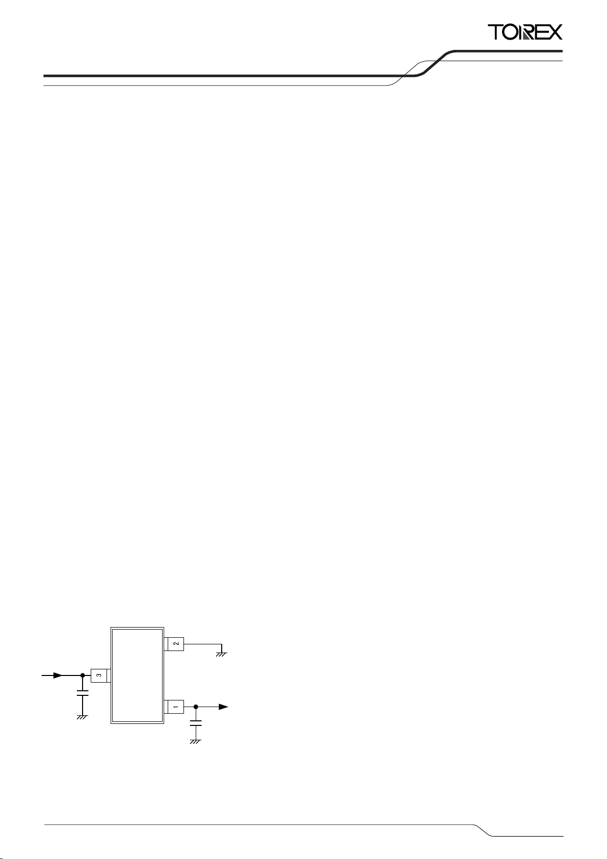
■TYPICAL APPLICATION CIRCUIT
IN
-V
CIN=1μF
(ceramic)
GND
-VOUT
IN=1μF
C
(ceramic)
■FEATURES
Input Voltage Range
Output Voltage Range
Accuracy
Temperature Stability
Dropout Voltage
Low Power Consumption
Protection Circuits
Output Capacitor
Operating Ambient
Temperature
Packages
Environmentally Friendly
: -2.4 ~ -16V
:
-2.5V,-2.6V,-3.0V,-3.3V,-4.0V,-4.5V,-5.0V,-6.0V,-12.0V
:
±1.5% for -2.0V~-12V
: TYP. ±50ppm/℃
: 400mV@I
: 100μA
:
Current Limit 350mA TYP. Foldback
=100mA
OUT
Thermal Shutdown (150℃)
: Ceramic Capacitor Compatible
:
-40℃~+85℃
: SOT-23, SOT-89, USP-6C
: EU RoHS Compliant, Pb Free
ETR0363-002
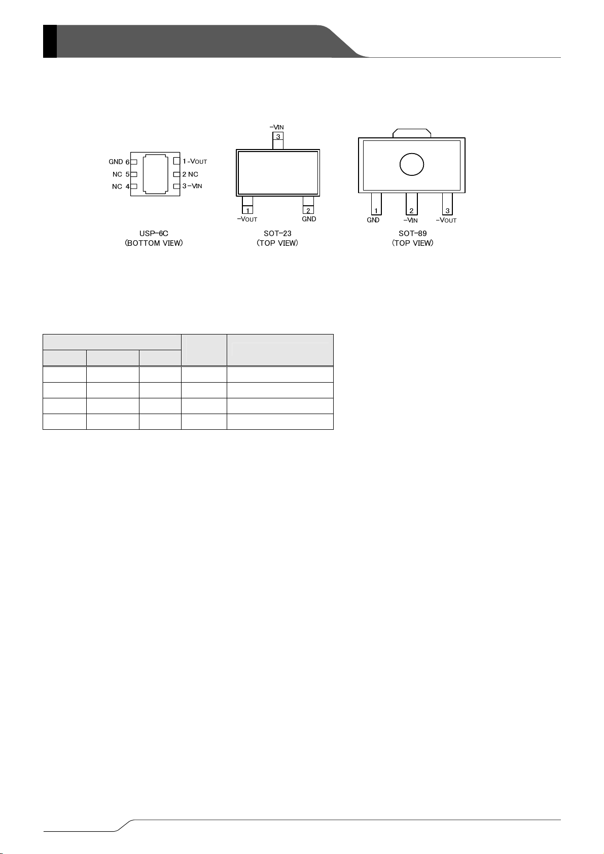
SOT-23
(TOP VIEW)
1/16
XC6902
Series
■PIN CONFIGURATION
* The dissipation pad for the USP-6C package should be solder-plated in recommended mount pattern and metal masking to enhance
mounting strength and heat release. If the pad needs to be connected to other pins, it should be connected to the -V
(No. 3) pin.
IN
■PIN ASSIGNMENT
PIN NUMBER
USP-6C SOT-23 SOT-89
3 3 2 -VIN Negative Supply Input
1 1 3 -V
6 2 1 GND Ground
2,4,5 - - NC No Connection
PIN
NAME
Negative Output
OUT
FUNCTIONS
2/16
■PRODUCT CLASSIFICATION
●Ordering Information
XC6902①②③④⑤⑥-⑦
DESIGNATOR ITEM SYMBOL DESCRIPTION
① Type N Soft-start, Thermal Shutdown
②③④
⑤⑥-⑦
(*1)
The “-G” suffix indicates that the products are Halogen and Antimony free as well as being fully RoHS compliant.
(*2)
For other output voltages, please contact your local Torex sales office or representative. The output voltage optional range is -0.9V to
-12V.
Output Voltage
(Order Unit)
(*1)
(Accuracy)
Packages
Three Terminal Voltage Regulator
251 -2.5V (±1.5%)
261 -2.6V (±1.5%)
301 -3.0V (±1.5%)
(*2)
331 -3.3V (±1.5%)
401 -4.0V (±1.5%)
451 -4.5V (±1.5%)
501 -5.0V (±1.5%)
601 -6.0V (±1.5%)
C01 -12.0V (±1.5%)
ER-G USP-6C(3,000/Reel)
MR-G
PR-G
SOT-23 (3,000/Reel)
SOT-89(1,000/Reel)
XC6902
Series
3/16

XC6902
Series
■ABSOLUTE MAXIMUM RATINGS
PARAMETER SYMBOL RATINGS UNITS
Input Voltage VIN GND-18 ~ GND+0.3 V
Output Current
Output Voltage V
Power
Dissipation
Operating Ambient Temperature
Storage Temperature Tstg -55~+125 ℃
(*1) Please use within the range of I
(*1)
I
USP-6C
SOT-23
SOT-89
≦Pd/(V
OUT
500 mA
OUT
V
OUT
1000 (PCB mounted)
Pd
Topr -40~+85 ℃
OUT-VIN
500 (PCB mounted)
1000 (PCB mounted)
)
■BLOCK DIAGRAM
GND=0V,Ta=25℃
-0.3 ~ VIN+18 V
IN
120
250
500
mW
4/16
*Diodes inside the circuit are an ESD protection diode and a parasitic diode.
■ELECTRICAL CHARACTERISTICS
XC6902
Series
●XC6902 Series
Ta=25℃
PARAMETER SYMBOL CONDITIONS MIN. TYP. MAX. UNITS CIRCUIT
V
<-2.0V
Output Voltage V
Maximum Output
(*4)
Current
OUT(E)
I
OUTMAX
Load Regulation ΔV
Dropout Voltage Vdif
Supply Current I
Input Line
Regulation
ΔV
(ΔV
V
(*2)
I
OUT
OUT
VIN=V
V
VIN=V
VIN=-4.0V
=20mA
OUT(T)
=-4.4V
IN
OUT(T)
-2.0V
-1.0V
1mA≦I
(*3)
I
V
BIAS
=-16V, I
IN
VIN:-16V~-2.4V V
VIN:-16V~
/
OUT
OUT
・
IN
)
V
-1V
OUT(T)
VIN:-16V~
V
-1V
OUT(T)
OUT(T)
≧-2.0V
V
OUT(T)
≦-2.4V
V
OUT(T)
V
>-2.4V
OUT(T)
V
≦-3.0V
OUT(T)
>-3.0V
V
OUT(T)
≦100mA
OUT
=20mA - E-1
OUT
=0mA - 100 200
OUT
>-1.4V
OUT(T)
-9≦V
=20mA
I
OUT
V
OUT(T)
OUT(T)
≦-1.4V
<-9.0V
Input Voltage VIN -16 - -2.4 V
Output Voltage
Temperature
Characteristics
Ripple Rejection
Ratio
Limit Current I
Short-Circuit
Current
ΔV
OUT
(ΔTopr・
V
OUT
PSRR
LIM
I
SHORT
/
)
={V
V
IN
VIN=V
OUT(T)
V
IN
=-4.4V
Short -V
=20mA
I
OUT
-40℃≦Topr≦85℃
-1.0}+0.5Vp-pAC,
OUT(T)
I
=20mA, f=1kHz
OUT
-2.0V
V
IN=VOUT(T)
to GND level
OUT
V
OUT(T)
V
OUT(T)
-2.0V
≦-2.4V
>-2.4V
×1.015 ×0.985
-0.030
V
OUT(T)
(*1)
V
+0.030
200 - - mA
- 20 60 mV
(*5)
mV
μA ①
- 0.05 0.20
%/V ①
- 0.1 0.30
- ±50 -
- 45 -
ppm/℃ ①
dB ②
210 300 - mA
- 80 - mA
①
①
①
①
①
①
①
Detect Thermal
Shutdown
T
TSD
℃ ①
IC Junction temperature - 150 -
Temperature
Release Thermal
Shutdown
T
TSR
℃ ①
IC Junction temperature - 125 -
Temperature
Hysteresis Width T
Soft Start Time tSS
T
HYS
(*6)
R
=3kΩ
L
- 25 -
TSD-TTSR
V
OUT(T)
V
OUT(T)
>-4.0V
≦-4.0V
℃ ①
0.12 0.4 1.2 ms
0.2 0.7 2 ms
③
③
NOTE:
The test condition for input voltage, Unless otherwise stated, GND=0V、V
*1) V
*2) V
*3)Vdif=-{V
: Nominal output voltage
OUT(T)
: Effective output voltage (see the voltage chart)
OUT(E)
(ie.The output voltage when “V
- V
OUT1
IN
}
pin.
IN1
is the input voltage when V
V
IN1
V
is the voltage equal to 98% of the normal output voltage when amply stabilized V
OUT1
are input at the V
-1.0V” or “-2.4V”is provided at the VIN pin while maintaining a certain I
OUT(T)
appears at the V
OUT1
pin while input voltage is gradually increased
OUT
IN=VOUT(T)
-1.0V or -2.4V.
-1.0V or -2.4V (the bigger absolute value one )
OUT(T)
OUT
value.
*4) The maximum current may not be able to flow when thermal shutdown operates, it depends on power dissipation.
*5) E-1:Refer to Dropout Voltage Chart.
*6) Input voltage condition is V
Soft-start time t
is defined as the time taken from the 90% rising of V
SS
=0V → V
IN
-1V with 5μs rising time.
OUT
to the 95% rising of V
IN
OUT(E).
5/16

XC6902
■ELECTRICAL CHARACTERISTICS(Continued)
Dropout Voltage Chart
NOMINAL
OUTPUT
VOLTAGE
V
OUT(T)
-2.50 129 174
-2.60 125 169
-3.00 110 151
-3.30 102 142
-4.00 91 127
-5.00 78 11 4
-6.0 70 105
-12.0 50 87
DROPOUT VOLTAGE
TYP. MAX.
Series
E-1
Vdif (mV)
6/16

■TEST CIRCUIT
1) CIRCUIT①
2) CIRCUIT②
XC6902
Series
3) CIRCUIT③
7/16

XC6902
Series
■OPERATIONAL EXPLANATION
The voltage divided by resistors R1 and R2 is compared with the internal reference voltage based on ground by the error
amplifier.
The driver transistor tied to the -V
controlled and stabilized by a system of negative feedback.
<Soft-Start Function>
The XC6902 series includes soft-start circuit. During power start-up, the inrush current from –V
capacitor can be reduced and it makes the V
Fugure1:Soft-Start Time and Inrush Current
<Current Limiter, Short-Circuit Protection>
The XC6902 series fold-back circuit operates as an output current limiter and a short protection circuit for the output pin. When the
output current reaches the current limit level, output voltage drops with the decrease of the output current.
There are no parasitic diode between the -V
pin voltage is pulled up toward positive.
<Thermal Shutdown>
The XC6902 Series has an internal thermal shutdown (TSD) circuit for protection against overheating.
When the junction temperature reaches the detection temperature, the driver transistor is forcibly turned off. When the junction
temperature falls to the release temperature with the driver transistor still in the off state, the driver transistor turns on (automatic
recovery) and restarts regulator operation.
pin is then driven by the subsequent output signal. The output voltage at the -V
IN
XC6902 Series
pin to V
IN
stable. Soft-start time (tSS) is optimized internally.
IN
pin and GND pin. The minimized short-circuit current is maintained even if the -V
OUT
pin to charge CL
OUT
OUT
pin is
OUT
8/16

XC6902
Series
■OPERATIONAL EXPLANATION (Continued)
Low ESR Capacitor>
<
With the XC6902 series, a stable output voltage is achievable even if used with low ESR capacitors, as a phase compensation
circuit is built-in. The output capacitor (C
compensation. Values required for the phase compensation are as the table below.
For a stable power input, please connect an input capacitor (C
compensation while avoiding run-out of values, please use the capacitor (C
too much. The table below shows recommended values of C
CHART 1:Recommended Values of CIN, CL
OUTPUT VOLTAGE
RANGE
V
OUT(T)
-0.9V~-12V 1.0μF~ 1.0μF~100μF
) should be connected as close to V
L
) near power supply. In order to ensure the stable phase
IN
IN
, CL.
IN
OUT
, CL ) which does not depend on bias or temperature
INPUT CAPACITOR OUTPUT CAPACITOR
CIN CL
pin and GND pin to obtain stable phase
■NOTES ON USE
1. Please use this IC within the stated maximum ratings. For temporary, transitional voltage drop or voltage rising
phenomenon, the IC is liable to malfunction should the ratings be exceeded.
2. Where wiring impedance is high, operations may become unstable due to noise and/or phase lag depending on output
current. Please keep the resistance low for the -V
3. Please wire the C
4. Capacitances of these capacitors (C
temperature. Care shall be taken for capacitor selection to ensure stability of phase compensation from the point of ESR
influence.
5. Torex places an importance on improving our products and its reliability.
However, by any possibility, we would request user fail-safe design and post-aging treatment on system or equipment.
IN and CL as close to the IC as possible.
IN, CL) are decreased by the influences of bias voltage and ambient
IN and GND wiring in particular.
9/16

XC6902
■PACKAGING INFORMATION
●SOT-23
●USP-6C
2.0±0.05
0.6MAX
1.0±0.05
0.70±0.05
Series
0.25±0.05
●SOT-89
Reference Pattern Layout Dimension
Reference Metal Mask Design
0.225
0.50.5
0.6
0.25
1.2
0.250.25
1.4
10/16

●SOT-23 Power Dissipation
Power dissipation data for the SOT-23 is shown in this page.
The value of power dissipation varies with the mount board conditions.
Please use this data as one of reference data taken in the described condition.
1. Measurement Condition (Reference data)
Condition : Mount on a board
Ambient : Natural convection
Soldering : Lead (Pb) free
Board : Dimensions 40×40mm(1600mm
2
in one side)
Copper (Cu) traces occupy 50% of the board area
In top and back faces
Package heat-sink is tied to the copper traces
(Board of SOT-26 is used)
XC6902
Series
Material : Glass Epoxy(FR-4)
Thickness : 1.6mm
Through-hole : 4 x 0.8 Diameter
2. Power Dissipation vs. Ambient temperature
Board Mount ( Tjmax=125℃)
Ambient Temperature (℃)
Power Dissipation Pd (mW)
25 500
85 200
Pd vs Ta
600
500
400
300
200
100
Power Dissipation Pd(mW)
0
25 45 65 85 105 125
Ambient Temperature Ta(℃)
Evaluation Board (Unit: mm)
Thermal Resistance (℃/W)
200.00
11/16

XC6902
Series
●SOT-89 Power Dissipation
Power dissipation data for the SOT-89 is shown in this page.
The value of power dissipation varies with the mount board conditions.
Please use this data as one of reference data taken in the described condition.
1. Measurement Condition (Reference data)
Condition : Mount on a board
Ambient : Natural convection
Soldering : Lead (Pb) free
Board : Dimensions 40×40mm(1600mm
2
in one side)
Copper (Cu) traces occupy 50% of the board area
In top and back faces
Package heat-sink is tied to the copper traces
Material : Glass Epoxy(FR-4)
Thickness : 1.6mm
Through-hole : 5 x 0.8 Diameter
28.9
40.0
2.5
2. Power Dissipation vs. Ambient temperature
Board Mount ( Tjmax=125℃)
Ambient Temperature (℃)
Power Dissipation Pd (mW)
25 1000
85 400
Pd vs Ta
1200
1000
800
600
400
200
Power Dissipation Pd(mW)
0
25 45 65 85 105 125
Ambient Temperature Ta(℃)
Thermal Resistance (℃/W)
100.00
12/16

●USP-6C Power Dissipation
Power dissipation data for the USP-6C is shown in this page.
The value of power dissipation varies with the mount board conditions.
Please use this data as one of reference data taken in the described condition.
1. Measurement Condition (Reference data)
Condition : Mount on a board
Ambient : Natural convection
Soldering : Lead (Pb) free
Board : Dimensions 40mm×40mm(1600mm
2
in one side)
Copper (Cu) traces occupy 50% of the board area
In top and back faces
Package heat-sink is tied to the copper traces
Material : Glass Epoxy(FR-4)
Thickness : 1.6mm
Through-hole : 4 x 0.8 Diameter
XC6902
Series
Evaluation Board (Unit: mm)
Evaluation Board (Unit: mm)
2. Power Dissipation vs. Ambient temperature(85℃)
Board Mount ( Tjmax=125℃)
Ambient Temperature (℃)
Power Dissipation Pd (mW)
25 1000
85 400
Thermal Resistance (℃/W)
100.00
13/16

XC6902
Series
■MARKING RULE
●SOT-23、SOT-89
① represents product series
MARK PRODUCT SERIES
E XC6902xxxxxx-G
② represents output voltage range
MARK
A
B
C
D -9.9 ~ -12.0
③ represents output voltage
3
① ② ③ ④ ⑤
12
SOT-23
VOLTAGE (V) PRODUCT SERIES
-0.9 ~ -3.8
-3.9 ~ -6.8
-6.9 ~ -9.8
③①
②
⑤
④
123
SOT-89
XC6902*091**-G ~ XC6902*381**-G
XC6902*391**-G ~ XC6902*681**-G
XC6902*691**-G ~ XC6902*981**-G
XC6902*991**-G ~ XC6902*C01**-G
MARK OUTPUT VOLTAGE (V) MARK OUTPUT VOLTAGE (V) MARK OUTPUT VOLTAGE (V)
0 -0.9 -3.9 -6.9 -9.9 A -1.9 -4.9 -7.9 -10.9 N -2.9 -5.9 -8.9 -11.9
1 -1.0 -4.0 -7.0 -10.0 B -2.0 -5.0 -8.0 -11.0 P -3.0 -6.0 -9.0 -12.0
2 -1.1 -4.1 -7.1 -10.1 C -2.1 -5.1 -8.1 -11.1 R -3.1 -6.1 -9.1 -
3 -1.2 -4.2 -7.2 -10.2 D -2.2 -9.2 --5.2 -8.2 -11.2 S -3.2 -6.2
4E
5 -1.4 -4.4 -7.4
6 -1.5 -4.5 -7.5
7 -1.6 -4.6 -7.6
8 -1.7 -4.7
9
-10.4
-10.5
-10.6
-7.7 -10.7
-10.8-1.8 -4.8 -7.8
F-2.4
H
K -2.6 -5.6
L -2.7 -5.7 -8.7
-5.4 -8.4
-2.5 -5.5 -8.5
-8.6 -11.6
-11.4
-11.5
-11.7
-11.8M -2.8 -5.8 -8.8
U -3.4 -6.4 -9.4
V -3.5 -6.5 -9.5 -
X -3.6 -6.6 -9.6
Y -3.7 -6.7 -9.7 -
-9.3 --2.3 -5.3 -8.3 -11.3 T -3.3 -6.3-1.3 -4.3 -7.3 -10.3
④⑤ represents production lot number
01~09, 0A~0Z, 11~9Z, A1~A9, AA~AZ、B1~ZZ repeated.
(G, I, J, O, Q, W excluded.)
* No character inversion used.
-
-
-Z -3.8 -6.8 -9.8
14/16

■MARKING RULE
●USP-6C
XC6902
Series
1
2
3
④ ⑤
USP-6C
② ③①
① represents product series
MARK PRODUCT SERIES
T XC6902xxxxxx-G
② represents output voltage range
MARK
A
B
C
VOLTAGE (V) PRODUCT SERIES
-0.9 ~ -3.8
-3.9 ~ -6.8
-6.9 ~ -9.8
D -9.9 ~ -12.0
③ represents output voltage
6
5
4
XC6902*091**-G ~ XC6902*381**-G
XC6902*391**-G ~ XC6902*681**-G
XC6902*691**-G ~ XC6902*981**-G
XC6902*991**-G ~ XC6902*C01**-G
MARK OUTPUT VOLTAGE (V) MARK OUTPUT VOLTAGE (V) MARK OUTPUT VOLTAGE (V)
0 -0.9 -3.9 -6.9 -9.9 A -1.9 -4.9 -7.9 -10.9 N -2.9 -5.9 -8.9 -11.9
1 -1.0 -4.0 -7.0 -10.0 B -2.0 -5.0 -8.0 -11.0 P -3.0 -6.0 -9.0 -12.0
2 -1.1 -4.1 -7.1 -10.1 C -2.1 -5.1 -8.1 -11.1 R -3.1 -6.1 -9.1 -
3 -1.2 -4.2 -7.2 -10.2 D -2.2 -9.2 --5.2 -8.2 -11.2 S -3.2 -6.2
4E
5 -1.4 -4.4 -7.4
6 -1.5 -4.5 -7.5
7 -1.6 -4.6 -7.6
8 -1.7 -4.7
9
-10.4
-10.5
-10.6
-7.7 -10.7
-10.8-1.8 -4.8 -7.8
F-2.4
H
K -2.6 -5.6
L -2.7 -5.7 -8.7
-5.4 -8.4
-2.5 -5.5 -8.5
-8.6 -11.6
-11.4
-11.5
-11.7
-11.8M -2.8 -5.8 -8.8
U -3.4 -6.4 -9.4
V -3.5 -6.5 -9.5 -
X -3.6 -6.6 -9.6
Y -3.7 -6.7 -9.7 -
-9.3 --2.3 -5.3 -8.3 -11.3 T -3.3 -6.3-1.3 -4.3 -7.3 -10.3
④⑤ represents production lot number
01~09, 0A~0Z, 11~9Z, A1~A9, AA~AZ、B1~ZZ repeated.
(G, I, J, O, Q, W excluded.)
* No character inversion used.
-
-
-Z -3.8 -6.8 -9.8
15/16

XC6902
Series
1. The products and product specifications contained herein are subject to change without
notice to improve performance characteristics. Consult us, or our representatives
before use, to confirm that the information in this datasheet is up to date.
2. We assume no responsibility for any infringement of patents, patent rights, or other
rights arising from the use of any information and circuitry in this datasheet.
3. Please ensure suitable shipping controls (including fail-safe designs and aging
protection) are in force for equipment employing products listed in this datasheet.
4. The products in this datasheet are not developed, designed, or approved for use with
such equipment whose failure of malfunction can be reasonably expected to directly
endanger the life of, or cause significant injury to, the user.
(e.g. Atomic energy; aerospace; transport; combustion and associated safety
equipment thereof.)
5. Please use the products listed in this datasheet within the specified ranges.
Should you wish to use the products under conditions exceeding the specifications,
please consult us or our representatives.
6. We assume no responsibility for damage or loss due to abnormal use.
7. All rights reserved. No part of this datasheet may be copied or reproduced without the
prior permission of TOREX SEMICONDUCTOR LTD.
16/16
 Loading...