

Page 1

F
XC6801 Series
ETR2502-004
1 Cell Li-ion Battery Linear Charger IC
with Constant-Current/Constant-Voltage
■GENERAL DESCRIPTION
The XC6801 series is a constant-current/constant-voltage linear charger IC for single cell lithium-ion batteries. The XC6801
includes a reference voltage source, battery voltage monitor, driver transistor, constant-current/constant-voltage charge circuit,
overheat protection circuit and phase compensation circuit. The battery charge termination voltage is internally set to 4.2V ±
0.7% and the trickle charge voltage and accuracy is 2.9V ±3%. In trickle charge mode, a safe battery charge is possible
because approximately only 1/10 of the full charge current is supplied to the battery. As it is possible to select a highly
accurate charge current of either 100mA (MAX.) for L level input to the L
for applications where the charge is from USB. The series’ charge status output pin, /CHG pin, is capable of checking the IC’s
charging state via connection to an external LED.
■APPLICATIONS
● USB charge applications
● Charging docks, charging cradles
● MP3 players, portable audio players
● Cellular phones, PDAs
● Bluetooth headsets
■TYPICAL APPLICATION CIRCUIT
■ FEATURES
Operating Voltage Range : 4.25V ~ 6.0V
Charge Current
(externally set)
Charge Termination Voltage : 4.2V ±0.7%
Trickle Charge Voltage : 2.9V ±3%
Supply Current (Stand-by)
Operating Ambient Tempera ture
Packages : SOT-89-5, SOT-25, USP-6C
Constant-current/constant-voltage operation
with thermal shutdown
Automatic recharge
Charge status output pin
Soft-start function (Inrush limit current)
Environmentally Friendly : EU RoHS Compliant, Pb Free
pin or 500mA (MAX.) for H level, the series is ideal
IM
: 100mA (MAX.) @ LIM pin=L
500mA (MAX.) @ L
: 12μA (TYP.)
: - 40℃~ + 85℃
■TYPICAL PERFORMANCE
CHARACTERISTICS
●Battery Charge Cycle
XC6801A421
1000
900
800
(mA)
700
BAT
600
500
400
300
Charge Current I
200
100
Char ge Cur ren t(Lim: H)
0
0 0.3 0.6 0.9 1.2 1.5
Time (hour)
V
=5V, CIN=1.0μ
IN=VLim
420mAh Battery
Battery Voltage
pin=H
IM
4.5
4.2
3.9
3.6
3.3
3.0
(V)
BAT
Battery Voltage V
1/19
Page 2

XC6801 Series
■PIN CONFIGURATION
■PIN ASSIGNMENT
SOT-25 SOT-89-5 USP-6C
■ FUNCTIONS
XC6801A421
PIN NUMBER
1 5 3 /CHG Charge Status Output Pin
2 2 2 VSS Ground
3 4 1 BAT Charge Current Pin
4 3 6 VIN Input Voltage Pin
5 1 4 LIM Changing Current Switch
- - 5 NC No Connection
PIN NAME CONDITIONS IC OPERATION
LIM
L
H
pin is left open, battery current is unstable. L
*If L
IM
■ PRODUCT CLASSIFICATION
●Ordering Information
XC6801A42①②③-④
* The dissipation pad for the USP-6C package should be solder-plated in recommended mount pattern and
metal masking so as to enhance mounting strength and heat release. If the pad needs to be connected to
other pins, it should be connected to the V
PIN NAME FUNCTION
0V≦V
1V≦V
≦0.4V
LIM
LIM
≦6V
(No. 2) pin.
SS
Charging Battery Current 1 (CC Mode)
Charging Battery Current 2 (CC Mode)
pin level should be fixed “High” or “Low”.
IM
DESIGNATOR ITEM SYMBOL DESCRIPTION
① Setting Charge Current 1 LIM”L”=95mA, LIM”H”=475mA
PR-G
MR-G
②③-④
(*1)
Packages
(Order Unit)
ER-G
(*1)
The “-G” suffix denotes Halogen and Antimony free as well as being fully RoHS compliant.
SOT-89-5 (1,000/Reel)
SOT-25 (3,000/Reel)
USP-6C (3,000/Reel)
2/19
Page 3

■BLOCK DIAGRAM
■ABSOLUTE MAXIMUM RATINGS
* Diodes inside the circuits are ESD protection diodes and parasitic diodes.
Ta =2 5℃
PAR AMETER SYMBOL RATINGS UNIT
VIN Pin Voltage VIN
LIM Pin Voltage VLIM
BAT Pin Voltage VBAT
/CHG Pin Voltage V/CHG
BAT Pin Current IBAT 900
Power Dissipation
SOT-25
SOT-89-5
USP-6C
Pd
-0.3 ~ +6.5
-0.3 ~ +6.5
-0.3 ~ +6.5
-0.3 ~ +6.5
(*1)
mA
250
600 (PCB mounted)
500
1300 (PCB mounted)
120
1000 (PCB mounted)
(*2)
(*2)
(*2)
Operating Ambient Temperature Topr - 40 ~ + 85 ℃
Storage Temperature Tstg - 55 ~ + 125 ℃
All voltages are described based on the VSS pin.
(*1) Please use within the range of I
(*2) The power dissipation figure shown is PCB mounted. Please refer to page 16 to 18 for details.
≦Pd/(VIN-V
BAT
BAT
).
V
V
V
V
mW
XC6801
Series
3/19
Page 4

XC6801 Series
■ELECTRICAL CHARACTERISTICS
XC6801A421
PAR AMETER SYMBOL CONDITIONS MIN TYP MAX UNIT CIRCUIT
Input Voltage VIN
Supply Current ISS
Stand-by Current I
Shut-down Current I
Float Voltage 1 V
Float Voltage 2
(*1)
V
Battery Current 1 I
Battery Current 2 I
Battery Current 3 I
Battery Current 4 I
Battery Current 5 I
Trickle Charge Current 1 I
Trickle Charge Current 2 I
STBY
SHUT
FLOAT1
FLOAT2
BAT1
BAT2
BAT3
BAT4
BAT5
TRIKL1
TRIKL2
Charge mode (V
Stand-by mode - 12 30
V
V
Shut-down mode
(VIN<V
or VIN<V
BAT
Ta=25℃, I
0℃≦Ta≦50℃, I
=3.8V, V
BAT
=3.8V, V
BAT
LIM
LIM
Stand-by mode, V
Shut-down mode - - 2.0
Stop mode, VIN=0V - - 2.0
V
BAT<VTRIKL(VLIM
V
BAT<VTRIKL(VLIM
LIM
=H or V
LIM
4.25 - 6.00 V
=L)
- 12 30
μA ③
μA ③
BAT
UVLO
=40mA
=40mA
BAT
)
- 8 18
×0.993 4.2 ×1.007 V
×0.99 4.2 ×1.01 V
μA ③
=L, CC mode 88 95 100 mA
=H, CC mode 440 475 500 mA
=4.2V - - 2.5
BAT
μA ③
μA ③
μA ③
=L )
=H )
7.5 9.5 12.0 mA
37.5 47.5 60.0 mA
Ta =2 5℃
-
②
③
③
③
③
Trickle Voltage V
Trickle Voltage
Hysteresis Width
UVLO Voltage V
UVLO Hysteresis Width V
VIN-V
BAT
Shut-down Voltage
VIN-V
Shut-down Voltage
BAT
Hysteresis Width
C/10 Charge Termination
Current Threshold
/CHG Pin
Weak Pull-Down Current
/CHG Pin
Strong Pull-Down Current
/CHG Pin
Output Low Voltage
Recharge Battery
Threshold Voltage
ON Resistance RON - 300 450 800 mΩ
Soft-Start Time tSS I
Recharge Battery Time t
Battery Termination
Detect Time
LIM Pin "H" Level Voltage V
LIM Pin "L" Level Voltage V
LIM Pin "H" Level Current I
LIM Pin "L" Level Current I
Thermal Shut-Down
Detect Temperature
Thermal Shut-Down
Release Temperature
Unless otherwise stated, VIN=5.0V.
(*1) The figures under the condition of 0
(*2) V
is a voltage to start recharging while reducing V
RECHRG
V
TRIKL
V
TRIKL_HYS
UVLO_HYS
V
ASD_HYS
I
I
V
ΔV
RECHRG
V
V
UVLO
- 150 190 280 mV
V
V
ASD
- 50 70 90 mV
I
TERM
V
/CHG1
V
/CHG2
I
/CHG
V
RECHRG
V
t
I
TERM
1 V
LIM_H
0.4 V
LIM_L
-0.1 0.1
LIM_H
-0.1 0.1
LIM_L
T
Junction temperature 120
TSD
T
Junction temperature 100
TSR
O
C≦Ta≦50OC are guaranteed by design calculation.
BAT
=L, V
LIM
=4.3V, V
BAT
=4.0V, V
BAT
FLOAT1-VRECHRG
= 0 → I
BAT
BAT
Rising 2.813 2.9 2.987 V
BAT
=L 58 90 116 mV
LIM
: L → H 3.686 3.8 3.914 V
IN
: L → H 70 100 140 mV
IN
V
=L 0.07 0.1 0.13 mA/mA
LIM
V
=H 0.07 0.1 0.13 mA/mA
LIM
/CHG
/CHG
=5mA - 0.35 0.60 V
/CHG
BAT2(VLIM
: H → L 0.4 1.7 3.2 ms
falling (Less than I
in stand-by mode from the full charge.
BAT
=5V 8 20 35
=1V 4 10 18 mA
(*2)
100 150 200 mV
=H) 120 150 180
) 0.3 1.2 2.4 ms
TERM
③
③
⑥
-
③
-
②
②
μA ③
③
④
③
①
μs ⑤
⑥
⑥
③
③
μA ①
μA ①
℃ -
℃ -
4/19
Page 5

Maintaini
Maintaini
)
≦
XC6801
Series
■OPERATIONAL DESCRIPTION
Constant-Current Charge (CC)
Constant-Voltage Charge (CV)
V
V
Charge Termination
<Charge Cycle>
If the BAT pin trickle voltage is less than 2.9V(TYP.), the charger enters trickle charge mode. In this mode, a safe battery
charge is possible because approximately only 1/10 of the charge current is supplied to the battery. When the BAT pin voltage
rises above trickle voltage, the charger enters constant-current mode (CC mode) and the battery is charged by the programmed
charge current. When the BAT pin voltage reaches 4.2V, the charger enters constant-voltage mode (CV mode) automatically.
After this, the charge current starts to drop and when it reaches a level which is 1/10 of the programmed charge current, the
charge terminates.
<Setting Charge Current>
The charge current can be set from 475mA(TYP.)or 95mA(TYP.)by the L
”H” level input:475mA(TYP.)
L
IM
L
”L” level input:95mA(TYP.)
IM
<Charge Termination>
The battery charge is terminated when the charge current decreases to 1/10 of the full charging level after the battery pin
voltage reaches a float voltage. An internal comparator monitors the I
the comparator sees that the I
A driver transistor turns off during the stand-by mode.
<Automatic Recharge>
In stand-by mode battery voltage falls. When the voltage level at the battery pin drops to recharge battery threshold voltage
4.05V(TYP.) or less, the charge cycle automatically re-start after a delay of 1.7ms. As such, no external activation control is
needed.
Charge Cycle
(Charge Main Routine)
Trickle Charge
V
>2.9V
BAT
-“L” I
I
LIM
BAT
BAT1
-“H” I
≦
I
LIM
BAT
BAT2
during a charge termin ation
detect time (1.2ms)
(Stand-by mode)
V
≦
4.05V
BAT
during a recharge time (1.7ms)
V
≦
2.9V
BAT
/10
/10
ng the charge state
ng the stand-by mode
Failure Detection
Input Voltage Monitor (UVLO) VIN-BAT Voltage Monitor (UVLO)
Shut-Down Shut-Down
VIN≧
3.8V
Charge Cycle Charge Cycle
VIN≧
3.61V
pin.
IM
pin voltage to detect the charge termination. When
pin voltage is less than 1.2ms (charge termination detect time), the IC enters stand-by mode.
SEN
SEN
△
(VIN-V
△(VIN-V
BAT
BAT
)>0.1V
<0.03V
No
Yes
5/19
Page 6

XC6801 Series
■OPERATIONAL EXPLANATION (Continued)
<Charge Condition Status>
The /CHG pin constantly monitors the charge states classified as below:
●Strong pull-down: I
●Weak pull-down: I
●High impedance: in shutdown mode.
<Connection of Shorted BAT Pin>
Even if the BAT pin is shorted to V
current.
<Under-voltage Lockout (UVLO)>
The UVLO circuit keeps the charger in shut-down mode until the input voltage, V
in order to protect the battery charger, the UVLO circuit keeps the charger in shut-down mode when the voltage between the
input pin voltage and BAT pin voltage falls to less than 30mV. The charge will not restart until the voltage between the input pin
voltage and BAT pin voltage rises more than 100mV. During shut-down mode, the driver transistor turns off but a failure
detection circuit operates, and supply current is reduced to 8μA.
<Soft-Start Function>
To protect against inrush current from the input to the battery, soft-start time is optimized and internally set (150μs, TYP.).
<Backflow Prevention Between the BAT Pin and the V
A backflow prevention circuit protects against current flowing from the BAT pin to the V
higher than the V
IN
=10mA (TYP.) in a charge cycle,
/CHG
=20μA (TYP.) in a stand-by mode,
/CHG
, a trickle charge mode operates in order to protect the IC from destruction caused by over
SS
pin voltage.
Pin>
IN
, rises above the UVLO voltage. Moreover,
IN
pin even if the BAT pin voltage is
IN
6/19
Page 7

XC6801
Series
■NOTES ON USE
1. For temporary, transitional voltage drop or voltage rising phenomenon, the IC is liable to malfunction should the ratings be
exceeded.
2. Where wiring impedance is high, operations may become unstable due to noise and/or phase lag depending on output
current. Please wire the C
3. Torex places an importance on improving our products and their reliability.
We request that users incorporate fail-safe designs and post-aging protection treatment when using Torex products in their
systems.
as close to the IC as possible.
IN
7/19
Page 8
y
XC6801 Series
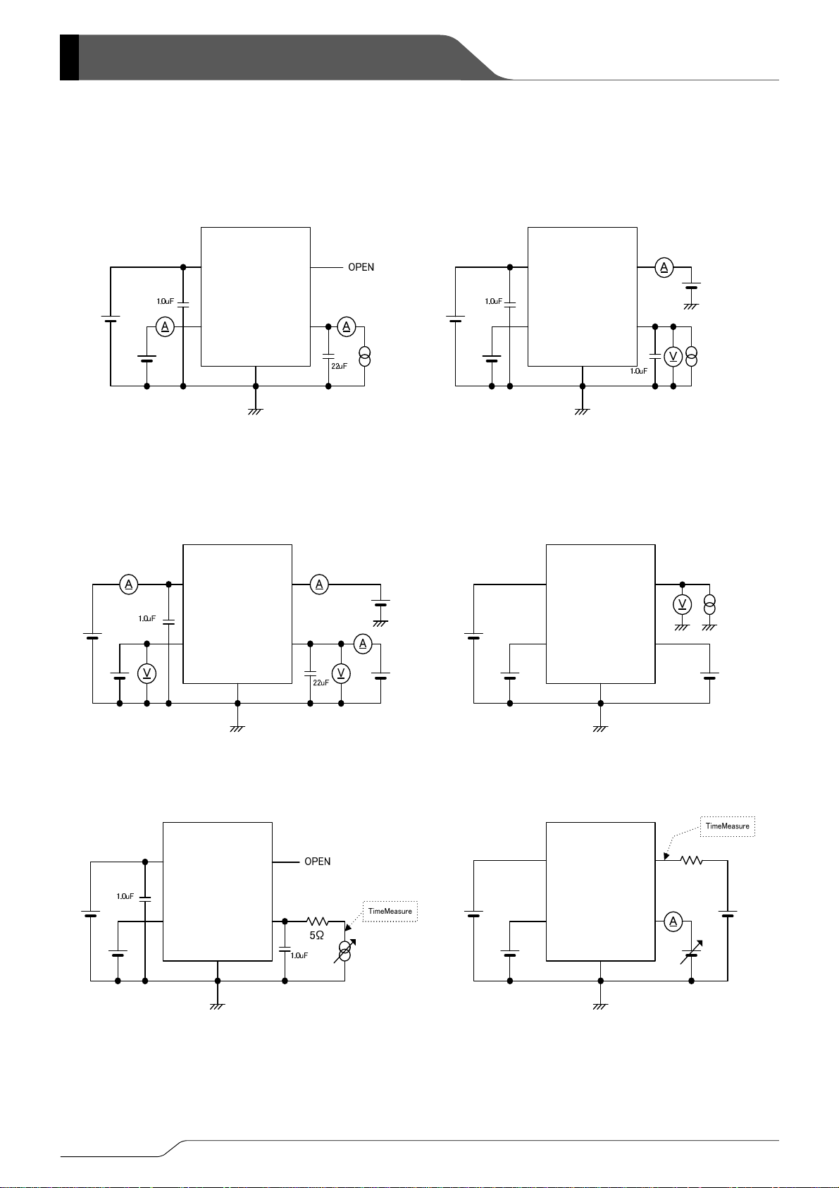
■TEST CIRCUITS
CIRCUIT①
測定回路①
1)
ON Resistance, L
抵抗、
ON
LIM端子"H"
L
Pin “L” level current,
IM
Pin “H” level current,
IM
レベル電流、
LIM端子"L"
レベル電流
CIRCUIT②
測定回路②
2)
C/10 Charge Termination Current Threshold,
充電完了電流閾値、充電完了電圧
C/10
Battery Termination Voltage1
1
V
IN
LIM
CIRCUIT③
測定回路 ③
3)
Trickle Charge Current1~2, Battery Current1~5,
トリクル充電電流1~2、バッテリー電流1~
L
Pin “H” level Voltage, LIM Pin “L” level Voltage,
IM
端子"H"レベル電圧、 LIM端子" L"レベ ル電圧
LIM
Trickle Charge Voltage, Recharge Battery Threshold Voltage,
トリクル電圧、 再充電しきい値電圧、
V
/CHG端子 Weak_Pull_down
消費電流、スタンバイ 電流、シャットダウン 電流
Shut-down Voltage, /CHG Pin Weak_Pull_down Current,
IN-VBAT
/CHG Pin Strong_Pull_down Current, Supply Current,
Stand-b
Current, Shut-down Current
5
V
IN-VBAT
電流、
/CHG端子 Strong_Pull_down
V
IN
LIM
V
/CHG
BAT
V
SS
間シャットダウン 電圧
/CH G
BAT
SS
電流
V
IN
LIM
V
SS
CIRCUIT④
測定回路④
4)
/CHG Pin Output Low Voltage
/CHG端子 出力LOW
電圧
V
LIM
IN
/CHG
V
SS
BAT
/CHG
BAT
CIRCUIT⑤
測定回路⑤
5)
Soft-Start Time
ソフトスタート時間
8/19
V
LIM
CIRCUIT⑥
測定回路⑥
6)
Recharge Time at Charge Termination Detect, UVLO Voltage
再充電時間、充電完了検出時間、
IN
/CH G
BAT
V
SS
V
LIM
IN
UVLO
電圧
V
/CHG
BAT
SS
Page 9

■TYPICAL PERFORMANCE CHARACTERISITCS
(1) Charge Cycle
(1)充電サイクル特性例
XC6801
Series
XC6801A421
V
IN=VLim
1000
900
800
(mA)
(mA)
700
BAT
BAT
600
Battery Voltege
バッテリー電圧
500
400
バッテリー電流
Battery Current
300
200
バッテリー電流 I
Battery Current: I
100
0
0 0.3 0.6 0.9 1.2 1.5
Charge Time (hour) Charge Time (hour)
充電時間 Time (hour)
(2) Battery Current vs. Battery Voltage
(2)定電流モード特性例
XC6801A421
120
100
(mA)
(mA)
BAT
80
BAT
=5V, CIN=1.0μF
420mAh Battery
V
=5V, V
IN
Lim
=0V
4.50
4.20
3.90
3.60
3.30
3.00
(V)
(V)
BAT
BAT
バッテリー電圧 V
Battery Voltage: V
XC6801A421
V
IN=VLim
1000
900
800
(mA)
(mA)
700
BAT
BAT
600
Battery Voltege
バッテリー電圧
500
400
300
200
バッテリー電流 I
Battery Current: I
100
Battery Current
バッテリー電流
0
0 0.3 0.6 0.9 1.2 1.5 1.8 2.1 2.4
充電時間 Time (hour)
XC6801A421
600
500
(mA)
(mA)
400
BAT
BAT
=5V, CIN=1.0μF
850mAh Battery
V
IN=VLim
4.50
4.20
3.90
3.60
3.30
3.00
=5V
(V)
(V)
BAT
BAT
バッテリー電圧 V
Battery Voltage: V
60
40
バッテリー電流 I
Battery Current: I
20
-40℃
25℃
85℃
0
3.5 3.6 3.7 3.8 3.9 4.0 4.1 4.2 4.3
バッテリー電圧 V
Battery Voltage: V
BAT
BAT
(V)
(V)
XC6801A421
120
100
(mA)
(mA)
80
BAT
BAT
60
VIN=4.5V
40
バッテリー電流 I
Battery Current: I
20
VIN=5.0V
VIN=5.5V
VIN=6.0V
0
3.5 3.6 3.7 3.8 3.9 4.0 4.1 4.2 4.3
バッテリー電圧 V
Battery Voltage: V
BAT
BAT
(V)
(V)
300
200
バッテリー電流 I
100
Battery Current: I
-40℃
25℃
85℃
0
3.5 3.6 3.7 3.8 3.9 4.0 4.1 4.2 4.3
Battery Voltage: V
バッテリー電圧 V
BAT
BAT
(V)
(V)
XC6801A421
V
=0V
V
Lim
600
Lim=VIN
500
(mA)
(mA)
400
BAT
BAT
300
VIN=4.5V
200
バッテリー電流 I
100
Battery Current: I
VIN=5.0V
VIN=5.5V
VIN=6.0V
0
3.5 3.6 3.7 3.8 3.9 4.0 4.1 4.2 4.3
Battery Voltage: V
バッテリー電圧 V
BAT
BAT
(V)
(V)
9/19
Page 10

XC6801 Series
■TYPICAL PERFORMACNE CHARACTORISTICS (Continued)
(3) Battery Voltage vs. Battery Current
(3)定電圧モード特性例
XC6801A421
4.25
(V)
4.20
(V)
BAT
BAT
4.15
4.10
-40℃
4.05
バッテリー電圧 V
Battery Voltage: V
25℃
85℃
4.00
50 60 70 80 90 100 110
Battery Current: I
バッテリー電流 I
BAT
BAT
XC6801A421
4.25
(V)
4.20
(V)
BAT
BAT
4.15
XC6801A421
V
=5V, V
IN
Lim
=0V
4.25
(V)
4.20
(V)
BAT
BAT
4.15
4.10
-40℃
4.05
バッテリー電圧 V
Battery Voltage: V
25℃
85℃
4.00
250 300 350 400 450 500 550
(mA) Battery Current: I
(mA)
バッテリー電流 I
XC6801A421
=0V
V
Lim
(V)
(V)
BAT
4.25
4.20
BAT
4.15
BAT
BAT
(mA)
(mA)
V
IN=VLim
V
Lim=VIN
=5V
4.10
Battery Voltage: V
4.05
バッテリー電圧 V
VIN=4.5V
VIN=5.0V
VIN=5.5V
VIN=6.0V
4.00
50 60 70 80 90 100 110
Battery Current: I
バッテリー電流 I
(4) Charge Termination Voltage vs. Ambient Temperature
(4)充電完了電圧 - 周囲温度特性例
(mA) Battery Current: I
(mA)
BAT
BAT
XC6801A421
(V)
4.24
VIN=5V, I
FLOAT1
=40mA, V
BAT
=0V
Lim
4.23
(V)
4.22
FLOAT1
4.21
4.20
4.19
4.18
充電完了電圧1 V
4.17
Charge Termination Voltage1: V
4.16
-50 -25 0 25 50 75 100
Ambient Temperature: Ta (℃)
周囲温度 Ta(℃)
4.10
VIN=4.5V
VIN=5.0V
Battery Voltage: V
4.05
バッテリー電圧 V
VIN=5.5V
VIN=6.0V
4.00
250 300 350 400 450 500 550
(mA)
BAT
バッテリー電流 I
BAT
(mA)
XC6801A421
(V)
FLOAT1
(V)
FLOAT
4.24
4.23
4.22
4.21
VIN=V
Lim
=5V, I
4.20
4.19
4.18
充電完了電圧 V
4.17
Charge Termination Voltage: V
4.16
-50 -25 0 25 50 75 100
Ambient Temperature: Ta (℃)
周囲温度 Ta(℃)
BAT
=200mA
10/19
Page 11

■TYPICAL PERFORMANCE CHARACTORISITCS (Continued)
(5) Battery Current vs. Ambient Temperature
(5)バッテリー電流 - 周囲温度特性例
XC6801
Series
XC6801A421
(mA)
(mA)
BAT1
BAT1
80
VIN=5V, V
90
=3.8V, V
BAT
Lim
=0V
100
110
Battery Current1: I
バッテリー電流1 I
120
-50 -25 0 25 50 75 100
周囲温度 Ta(℃)
Ambient Temperature: Ta (℃) Ambient Temperature: Ta (℃)
(6) Trickle Charge Current vs. Ambient Temperature
(6)トリクル充電電流 - 周囲温度特性例
XC6801A421
6
VIN=5V, V
(mA)
7
TRIKL1
(mA)
8
TRIKL1
9
BAT
=2.5V, V
Lim
=0V
10
11
12
13
トリクル充電電流1 I
Trickle Charge Current1: I
14
-50 -25 0 25 50 75 100
周囲温度 Ta(℃)
Ambient Temperature: Ta (℃) Ambient Temperature: Ta (℃)
XC6801A421
VIN=V
=5V, V
Lim
(mA)
(mA)
BAT2
BAT2
460
480
500
520
Battery Current2: I
バッテリー電流2 I
540
-50 -25 0 25 50 75 100
周囲温度 Ta(℃)
XC6801A421
VIN=V
=5V, V
30
(mA)
35
TRIKL2
(mA)
40
TRIKL2
45
Lim
50
55
60
65
トリクル充電電流2 I
Trickle Charge Current2: I
70
-50 -25 0 25 50 75 100
周囲温度 Ta(℃)
BAT
BAT
=3.8V
=2.5V
(7) Trickle Voltage vs. Ambient Temperature
(7)トリクル電圧 - 周囲温度特性例 (8)UVLO電圧 - 周囲温度特性例
XC6801A421
VIN=5V
3.00
2.95
(V)
(V)
2.90
TRIKL
TRIKL
2.85
(8) UVLO Voltage vs. Ambient Temperature
XC6801A421
3.95
3.85
(V)
(V)
UVLO
3.75
UVLO
3.65
2.80
2.75
トリクル電圧 V
Trickle Voltage: V
2.70
Trickle Voltage (Release)
トリクル電圧(解除)
トリクル電圧(検出)
Trickle Voltage (Detect)
2.65
-50 -25 0 25 50 75 100
周囲温度 Ta(℃)
Ambient Temperature: Ta (℃) Ambient Temperature: Ta (℃)
3.55
UVLO電圧 V
UVLO Voltage: V
3.45
UVLO Voltage (Detect)
UVLO電圧(検出)
UVLO Voltage (Release)
UVLO電圧(解除)
3.35
-50 -25 0 25 50 75 100
周囲温度 Ta(℃)
11/19
Page 12

XC6801 Series
■TYPICAL PERFORMANCE CHARACTORISTICS (Continued)
(9)VIN-VBAT間シャットダウン電圧 - 周囲温度特性例
(9) VIN – V
(V)
ASD
ASD
Shutdown Voltage vs. Ambient Temperature
BAT
XC6801A421
200
VIN-VBAT間シャットダウン電圧(検出)
VIN-V
Shutdown Voltage (Detect)
BAT
VIN-V
160
Shutdown Voltage (Release)
VIN-VBAT間シャットダウン電圧(解除)
BAT
120
(V)
80
間シャットダウン解除電圧 V
40
Shutdown Release Voltage: V
BAT
-V
BAT
IN
V
0
– V
IN
-50 -25 0 25 50 75 100
V
周囲温度 Ta(℃)
Ambient Temperature: Ta (℃) Ambient Temperature: Ta (℃)
(11)再充電時間 - 周囲温度特性例 (12)再充電しきい値電圧 - 周囲温度特性例
(11) Recharge Time vs. Ambient Temperature
XC6801A421
3.0
2.5
(ms)
VIN=5V
(ms)
2.0
RECHRG
RECHRG
(10) Charge Termination Detect Time vs. Ambient Temperature
(10)充電完了検出時間 - 周囲温度特性例
XC6801A421
2.5
(ms)
TERM
(ms)
2.0
TERM
1.5
1.0
0.5
充電完了検出時間 T
0.0
-50 -25 0 25 50 75 100
Charge Termination Detect Time: t
周囲温度 Ta(℃)
(12) Recharge Threshold Voltage vs. Ambient Temperature
XC6801A421
(mV)
220
RECHRG
(mV)
200
RECHRG
180
160
1.5
140
1.0
0.5
再充電時間 T
Recharge Time: t
0.0
-50 -25 0 25 50 75 100
周囲温度 Ta(℃)
Ambient Temperature: Ta (℃) Ambient Temperature: Ta (℃)
120
100
再充電しきい値電圧 △V
80
-50 -25 0 25 50 75 100
Recharge Threshold Voltage: △V
周囲温度 Ta(℃)
VIN=5V
VIN=5V
(13)ソフトスタート時間 - 周囲温度特性例 (14)ON抵抗 - 周囲温度特性例
(13) Soft Start Time vs. Ambient Temperature
XC6801A421
(14) ON Resistance vs. Ambient Temperature
XC6801A421
VIN=5V
220
200
(μs)
(μs)
180
SS
ss
160
140
120
Soft Start Time: t
100
ソフトスタート時間 T
80
-50 -25 0 25 50 75 100
周囲温度 Ta(℃)
Ambient Temperature: Ta (℃) Ambient Temperature: Ta (℃)
1.0
0.8
(Ω)
ON
(Ω)
0.6
ON
0.4
ON抵抗 R
0.2
ON Resistance: R
0.0
-50 -25 0 25 50 75 100
周囲温度 Ta(℃)
12/19
VIN=4.15V, I
=100mA
BAT
Page 13

■TYPICAL PERFORMANCE CHARACTORISTCS (Continued)
XC6801
Series
(15) Shutdown Current vs. Ambient Temperature
(15)シャットダウン電流 - 周囲温度特性例 (16)スタンバイ電流 - 周囲温度特性例
XC6801A421
VIN=5V
25
20
(μA)
(μA)
Shut
SHUT
15
10
(16) Stand-by Current vs. Ambient Temperature
XC6801A421
35
30
(μA)
(μA)
25
STBY
Stby
20
15
VIN=5V, V
10
5
シャットダウン電流 I
Shutdown Current: I
0
-50 -25 0 25 50 75 100
周囲温度 Ta(℃)
Ambient Temperature: Ta (℃)
(17)/CHG Weak Pull Down電流特性例 (18)/CHG Strong Pull Down電流特性例
(17) /CHG Weak Pull Down Current vs. /CHG Pin Voltage
XC6801A421
(μA)
45
CHG1
40
(μA)
chg1
35
30
-40℃
25℃
85℃
25
20
V
=5V, V
IN
BAT
=4.3V
スタンバイ電流 I
5
Stand-by Current: I
0
-50 -25 0 25 50 75 100
Ambient Temperature: Ta (℃)
周囲温度 Ta(℃)
(18) /CHG Strong Pull Down Current vs. /CHG Pin Voltage
XC6801A421
V
=5V, V
(mA)
(mA)
CHG2
chg2
25
20
15
10
-40℃
25℃
85℃
IN
15
10
5
5
/CHG Weak_Pull_Down電流 I
0
/CHG Weak Pull Down Current: I
0.0 1.0 2.0 3.0 4.0 5.0 6.0
/CHG Pin Voltage: V
/CHG端子電圧 V
CHG
CHG
(V)
(V)
/CHG Strong_Pull_Down電流 I
0
0123456
/CHG Strong Pull Down Current: I
/CHG Pin Voltage: V
/CHG端子電圧 V
CHG
CHG
(V)
(V)
BAT
BAT
=4.3V
=4.0V
(19) /CHG Pin Output Low Voltage vs. Ambient Temperature
(19)/CHG端子出力LOW電圧 - 周囲温度特性例
XC6801A421
(V)
CHG
(V)
=5mA, VIN=5V, V
1.0
/CHG
0.9
/CHG
0.8
BAT
=2.5V
I
0.7
0.6
0.5
0.4
0.3
0.2
0.1
/CHG端子 出力LOW電圧 V
0.0
/CHG Pin Output Low Voltage: V/
-50 -25 0 25 50 75 100
周囲温度 Ta(℃)
Ambient Temperature: Ta (℃)
13/19
Page 14
XC6801 Series
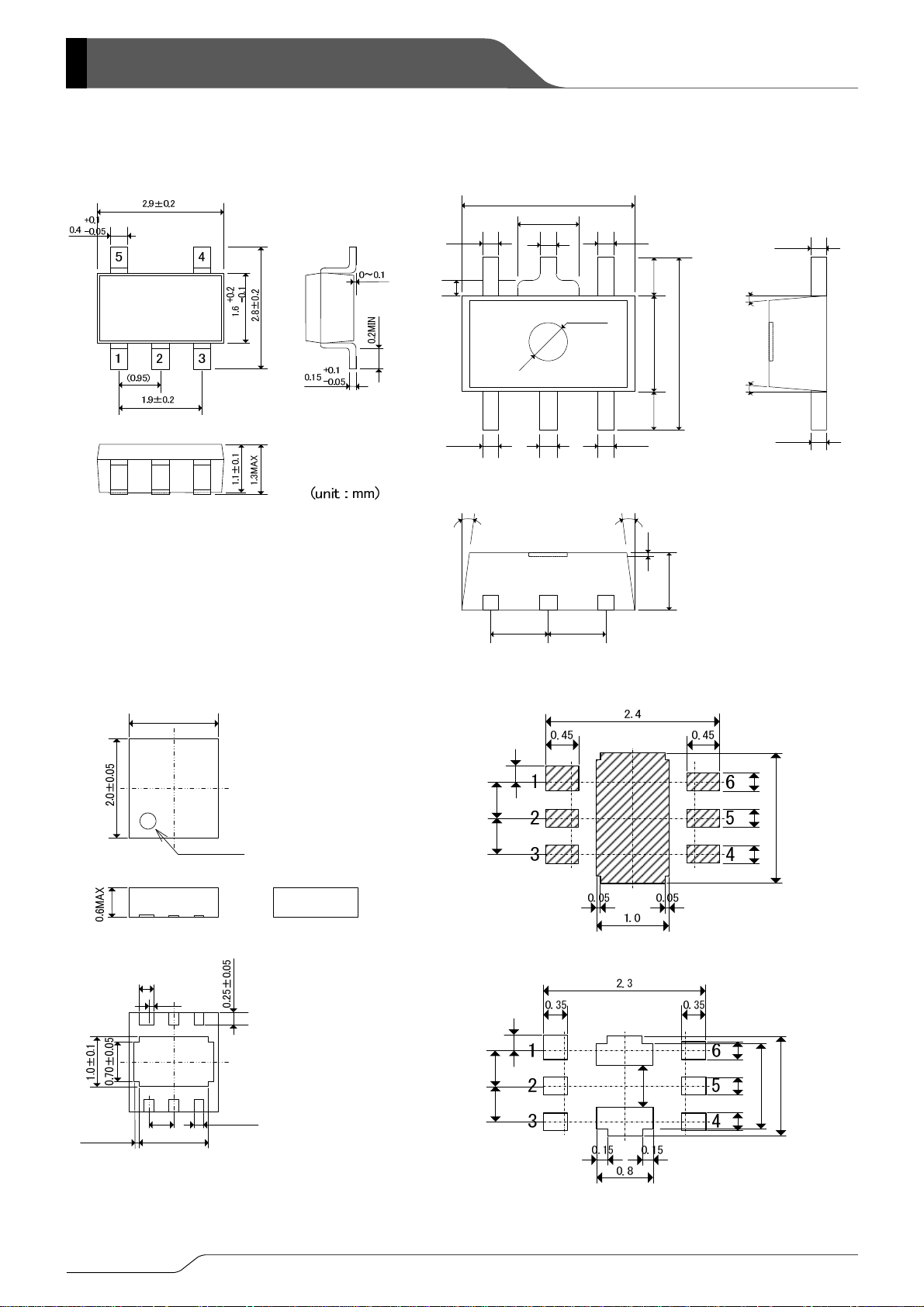
■PACKAGING INFORMATION
●SOT-25
●USP-6C
1.8±0.05
1pin INDENT
0.30±0.05
(0.10)
●SOT-89-5
0.42±0.06
(0.4)
0.42±0.06 0.42±0.060.47±0.06
8°
0.42±0.06
5
123
1.5±0.1 1.5±0.1
●USP-6C Reference Pattern Layout
0.225
0.50.5
●USP-6C Reference Metal Mask Design
4.5±0.1
+0.15
1.6
-0.2
2
Φ1.0
0.42±0.06
4
8°
0.8 MIN
2.5±0.10.8 MIN
4.35 MAX
(0.1)
1.5±0.1
5°
5°
0.4
0.4
(unit : mm)
0.25
1.8
0.250.25
+0.03
-0.02
+0.03
-0.02
0.10±0.05
14/19
0.50
1.4±0.1
0.20±0.05
(unit : mm)
0.225
0.50.5
0.6
0.25
1.2
0.250.25
1.4
Page 15

■MARKING RULE
SOT25
SOT-25
54
① represents product series
MARK PRODUCT SERIES
① ② ③ ④ ⑤
123
② represents the 7th digits
4 XC6801******-G
MARK PRODUCT SERIES
SOT89-5
SOT-89-5
524
③①
②
123
⑤
④
③ represents the 8th digits
④⑤ represents production lot number
A XC6801A*****-G
MARK PRODUCT SERIES
4
XC6801*4****-G
01~09, 0A~0Z, 11・・・9Z, A1・・・A9, AA ・・・Z9, ZA・・・ZZ in order.
USP-6C
USP6C
*No character inversion used.
(G, I, J, O, Q, W excepted)
1
2
3
①
④ ⑤
6
②
5
③
4
XC6801
Series
15/19
Page 16

XC6801 Series
■PACKAGING INFORMATION (Continued)
● SOT-89-5 Power Dissipation
Power dissipation data for the SOT-89-5 is shown in this page.
The value of power dissipation varies with the mount board conditions.
Please use this data as one of reference data taken in the described condition.
1. Measurement Condition (Reference data)
Condition: Mount on a board
Ambient: Natural convection
Soldering: Lead (Pb) free
Board: Dimensions 40 x 40 mm (1600 mm
Copper (Cu) traces occupy 50% of the board area
Material: Glass Epoxy (FR-4)
Thickness: 1.6 mm
Through-hole: 5 x 0.8 Diameter
2. Power Dissipation vs. Ambient Temperature
Board Mount (Tj max = 125℃)
In top and back faces
Package heat-sink is tied to the copper traces
2
in one side)
Evaluation Board (Unit: mm)
Ambient Temperature(℃) Power Dissipation Pd(mW) Thermal Resistance (℃/W)
25 1300
76.92
85 520
Pd-Ta特性グラフ
Pd vs. Ta
1400
1200
1000
800
600
400
200
許容損失Pd(mW)
Power Dissipation Pd (mW)
0
25 45 65 85 105 125
Ambient Temperature Ta (℃)
周辺温度Ta(℃)
16/19
Page 17

XC6801
Series
■PACKAGING INFORMATION (Continued)
● SOT-25 Power Dissipation
Power dissipation data for the SOT-25 is shown in this page.
The value of power dissipation varies with the mount board conditions.
Please use this data as one of reference data taken in the described condition.
1. Measurement Condition (Reference data)
Condition: Mount on a board
Ambient: Natural convection
Soldering: Lead (Pb) free
Board: Dimensions 40 x 40 mm (1600 mm
Copper (Cu) traces occupy 50% of the board area
Material: Glass Epoxy (FR-4)
Thickness: 1.6 mm
Through-hole: 4 x 0.8 Diameter
2. Power Dissipation vs. Ambient Temperature
Board Mount (Tj max = 125℃)
In top and back faces
Package heat-sink is tied to the copper traces
(Board of SOT-26 is used.)
2
in one side)
Evaluation Board (Unit: mm)
Ambient Temperature(℃) Power Dissipation Pd(mW) Thermal Resistance (℃/W)
25 600
166.67
85 240
Pd-Ta特性グラフ
Pd vs. Ta
700
600
500
400
300
200
100
許容損失Pd(mW)
Power Dissipation Pd (mW)
0
25 45 65 85 105 125
Ambient Temperature Ta (℃)
周辺温度Ta(℃)
17/19
Page 18
XC6801 Series
■PACKAGING INFORMATION (Continued)
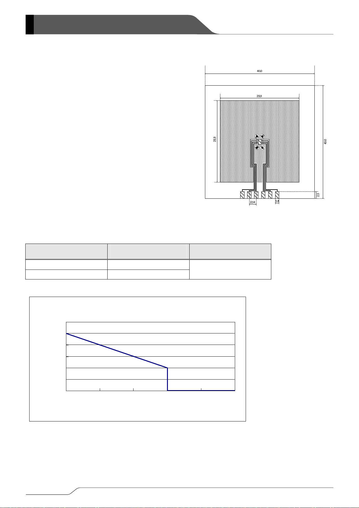
● USP-6C Power Dissipation
Power dissipation data for the USP-6C is shown on this page.
The value of power dissipation varies with the mount board conditions.
Please use this data as one of reference data taken in the described condition.
1. Measurement Condition (Reference data)
Condition: Mount on a board
Ambient: Natural convection
Soldering: Lead (Pb) free
Board: Dimensions 40 x 40 mm (1600 mm
Copper (Cu) traces occupy 50% of the board area
In top and back faces
Package heat-sink is tied to the copper traces
Material: Glass Epoxy (FR-4)
Thickness: 1.6 mm
Through-hole: 4 x 0.8 Diameter
Evaluation Board (Unit: mm)
2. Power Dissipation vs. Ambient Temperature
Board Mount (Tj max = 125℃)
2
in one side)
Ambient Temperature(℃) Power Dissipation Pd(mW) Thermal Resistance (℃/W)
25 1000
100
85 400
Pd vs. Ta
1200
1000
800
600
400
200
0
Power Dissipation Pd(mW)
25 45 65 85 105 125
Ambient Temperature Ta(℃)
18/19
Page 19

XC6801
Series
1. The products and product specifications contained herein are subject to change without
notice to improve performance characteristics. Consult us, or our representatives
before use, to confirm that the information in this datasheet is up to date.
2. We assume no responsibility for any infringement of patents, patent rights, or other
rights arising from the use of any information and circuitry in this datasheet.
3. Please ensure suitable shipping controls (including fail-safe designs and aging
protection) are in force for equipment employing products listed in this datasheet.
4. The products in this datasheet are not developed, designed, or approved for use with
such equipment whose failure of malfunction can be reasonably expected to directly
endanger the life of, or cause significant injury to, the user.
(e.g. Atomic energy; aerospace; transport; combustion and associated safety
equipment thereof.)
5. Please use the products listed in this datasheet within the specified ranges.
Should you wish to use the products under conditions exceeding the specifications,
please consult us or our representatives.
6. We assume no responsibility for damage or loss due to abnormal use.
7. All rights reserved. No part of this datasheet may be copied or reproduced without the
prior permission of TOREX SEMICONDUCTOR LTD.
19/19
 Loading...