

Page 1
XC6365/XC6366 Series
ETR0501_005a
PWM Controlled, PWM/PFM Switchable Step-Down DC/DC Controllers
■GENERAL DESCRIPTION
The XC6365/XC6366 series are multi-functional step-down DC/DC controllers which have 1A output current capability by
using an externally connected transistor, coil, diode and capacitor.
Output voltage is programmable in 0.1V increments between 1.5V to 6.0V (V
standard voltage supply internal and using externally connected components, output voltage can be set up freely (FB). With
a 300kHz switching frequency, the size of the external components can be reduced.
Control switches from PWM to PFM during light loads with the XC6366 (PWM/PFM switchable) and the series is highly
efficient from light loads to large output currents.
Soft start time of XC6365/ XC6366A, B series is internally set to 10ms and XC6365/66C, D series regulate soft-start time by
connecting resistors and capacitors externally.
During stand-by time (CE pin "Low" ), current consumption is reduced to less than 0.5μA.
With UVLO internal, the external transistor will be forcibly switched off if used below the stipulated voltage.
■APPLICATIONS
●Electronic information organizers
●Palmtops
●Cellular and portable phones
●Portable audio systems
●Various multi-function power supplies
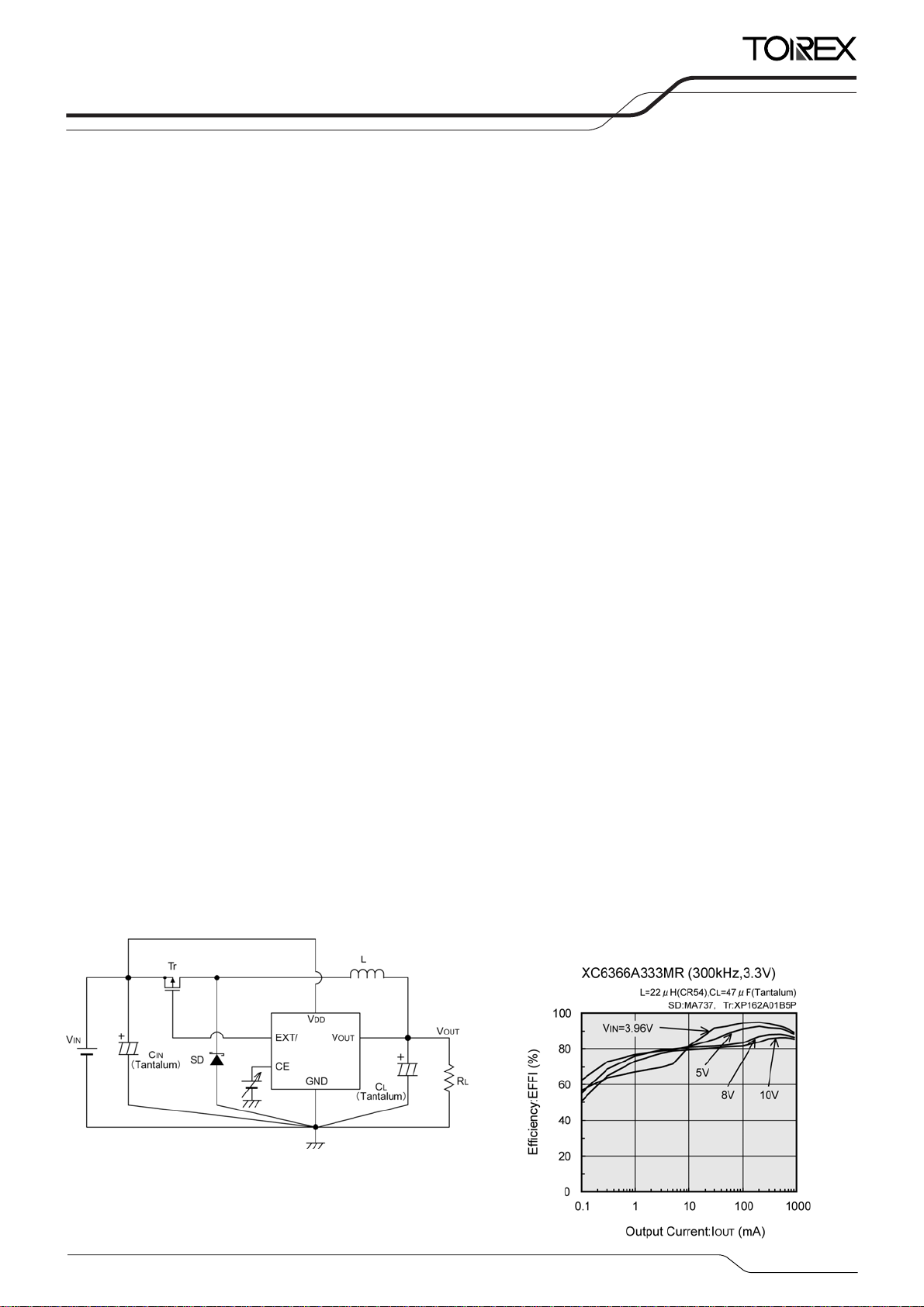
■TYPICAL APPLICATION CIRCUIT
■FEATURES
Input Voltage Range : 2.2V ~ 10V (VOUT type)
Output Voltage Range
Oscillation Frequency
Output Current : More than 1.0A (V
High Efficiency : 92% (TYP.)
Stand-by Capability : I
Selection : Soft-start set-up external
Maximum Duty Cycle : 100%
Packages : SOT-25, USP-6C
Environmentally Friendly :
■TYPICAL PERFORMANCE
CHARACTERISTICS
OUT) (±2.5% accuracy). Further, with 1.0V of
☆GreenOperation Compatible
: 1.5V ~ 6.0V (0.1V increments) (±2.5%)
: 300kHz (±15%)
Custom products for 180, 500kHz
IN=5.0V, VOUT=3.0V)
=0.5μA (MAX.)
STB
Output voltage set-up internal (V
Output voltage set-up external (FB)
PWM/PFM Control (XC6366)
EU RoHS Compliant, Pb Free
OUT)
1/24
Page 2
XC6365/XC6366 Series
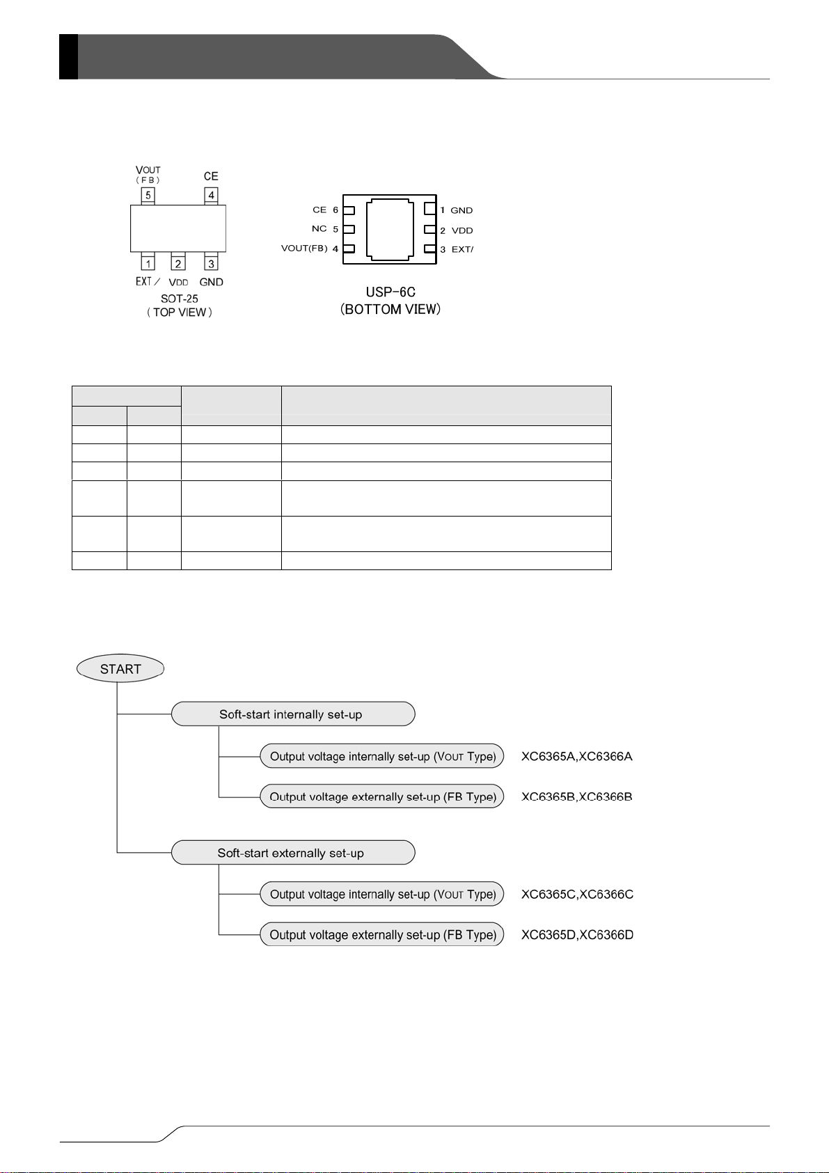
■PIN CONFIGURATION
■PIN ASSIGNMENT
PIN NUMBER
SOT-25
USP-6
PIN NAME FUNCTION
1 3 EXT/ External Transistor Connection
2 2 VDD Power Supply
3 1 GND Ground
4 6 CE
5 4 VOUT (FB)
-
■PRODUCT CLASSIFICATION
●Selection Guide
5 NC No Connection
Chip Enable Soft-Start Capacitor Connection
with Soft-Start Externally Set-Up Types (C, D)
Output Voltage Monitor FB with Externally
Set-Up Types (B, D)
*The dissipation pad of the USP-6C package
should be left open. If the circuit needs to be
connected to other pin, it should be connected to
the V
DD (No.2) pin.
2/24
Page 3

■PRODUCT CLASSIFICATION (Continued)
●Ordering Information
XC6365①②③④⑤⑥-⑦
XC6366①②③④⑤⑥-⑦
(*1)
PWM control
(*1)
PWM/PFM switching control
DESIGNATOR ITEM SYMBOL DESCRIPTION
A VOUT type: Internally set-up, soft-start internally set-up
①
Type of DC/DC Converter
B FB type: Externally set-up, soft-start internally set-up
C VOUT type: Internally set-up, soft-start externally set-up
D FB type: Externally set-up, soft-start internally set-up
②③
Output Voltage
15~60 VOUT type: 3.0V output → ②=3, ③=0
10
FB type: 10 fixed → ②=1, ③=0 fixed
3 300kHz
④
Oscillation Frequency
5 500kHz (custom)
2 180kHz (custom)
MR SOT-25 (3,000/Reel)
⑤⑥-⑦
Packages
(Order Unit)
MR-G SOT-25 (3,000/Reel)
ER USP-6C (3,000/Reel)
ER-G USP-6C (3,000/Reel)
(*1)
The “-G” suffix indicates that the products are Halogen and Antimony free as well as being fully RoHS compliant.
XC6365/XC6366
Series
3/24
Page 4
XC6365/XC6366 Series
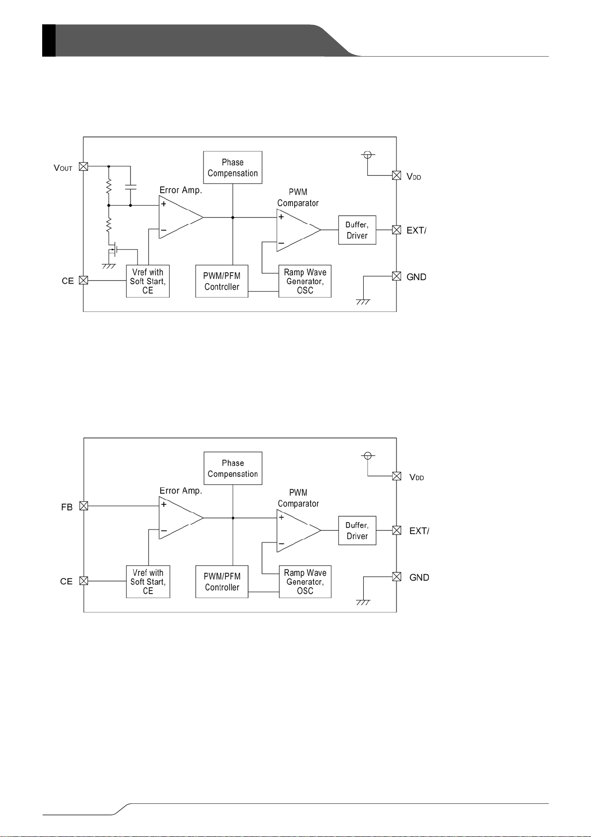
■BLOCK DIAGRAMS
XC6365, XC6366 Series A, C type (VOUT)
XC6365, XC6366 Series B, D type (FB)
4/24
Page 5
XC6365/XC6366
Series
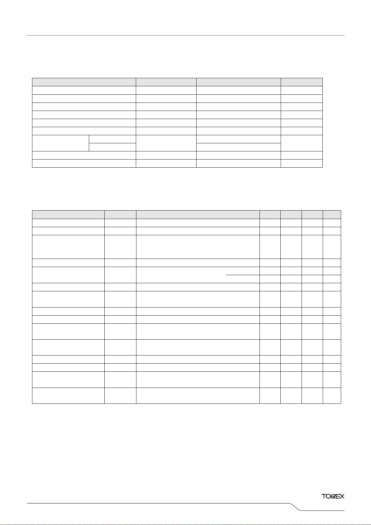
■ABSOLUTE MAXIMUM RATINGS
PAR AMETER SYMBOL RATINGS UNITS
VIN Pin Voltage VDD -0.3 ~ +12 V
VOUT Pin Voltage VOUT -0.3 ~ VIN +0.3 V
FB Pin Voltage VFB -0.3 ~ VIN +0.3 V
CE Pin Voltage VCE -0.3 ~ VIN +0.3 V
EXT/ Pin Voltage VEXT/ -0.3 ~ VIN +0.3 V
EXT/ Pin Current
Power Dissipation
SOT-25 150
USP-6C
IEXT/
Pd
±100
100
Operating Temperature Range Topr -30 ~ +80
Storage Temperature Range Tstg -40 ~ +125
Note: Voltage is all ground standardized.
■ELECTRICAL CHARACTERISTICS
XC6365A333MR, XC6366A333MR
(VOUT=3.3V, f
=300kHz)
OSC
PAR AMETER SYMBOL CONDITIONS MIN. TYP. MAX. UNITS
Output Voltage VOUT 3.218 3.300 3.383 V
Maximum Input Voltage VIN 10.0 - - V
UVLO Voltage
(Minimum Operating
Voltage)
V
UVLO
Same as I
Voltage which EXT/pin voltage holding “H” level
DD1,
0.9 - 2.2 V
Supply Current 1 IDD1 No external components, CE=VDD, VOUT=0V - 57 102
Supply Current 2 IDD2
No external components,
CE=V
OUT=VDD
XC6365 - 57 102
XC6366 - 15 27
Stand-by Current ISTB No external components, CE=VOUT=0V - - 0.5
Oscillation Frequency f
OSC
Measuring of EXT/ waveform,
VIN=output voltage + 0.1V
255 300 345 kHz
Maximum Duty Ratio MAXDTY 100 - - %
PFM Duty Ratio PFMDTY No load (XC6366 only) 15 25 35 %
CE "High" Voltage VCEH
CE "Low" Voltage VCEL
No external components, V
Voltage which EXT/pin voltage holding “L” level
No external components, V
Voltage which EXT/pin voltage holding “H” level
OUT=0V,
OUT=0V,
0.65 - - V
- - 0.20 V
EXT "High" ON Resistance REXTBH Same as IDD2, VEXT/=VDD-0.4V - 16 22
EXT "Low" ON Resistance REXTBL Same as IDD1, VEXT/=0.4V - 14 19
Efficiency EFFI
Soft-Start Time tSS
Conditions: 1. Unless otherwise stated, connect external components. VIN=VDD = 5.0V, IOUT = 220mA
2. XC6365/66C series external components: C
Use of a XP162A12A6 transistor
recommended
Connect R
(When V
SS, CSS, CE, 0V→ 3.0V
IN≦3.0V, VIN=3.0V)
SS=0.033μF, R SS=470kΩ
- 92 - %
5 10 20
Ta = 2 5℃
mA
mW
℃
℃
Ta =2 5℃
μA
μA
μA
μA
μA
μA
ms
5/24
Page 6
XC6365/XC6366 Series
■ELECTRICAL CHARACTERISTICS (Continued)
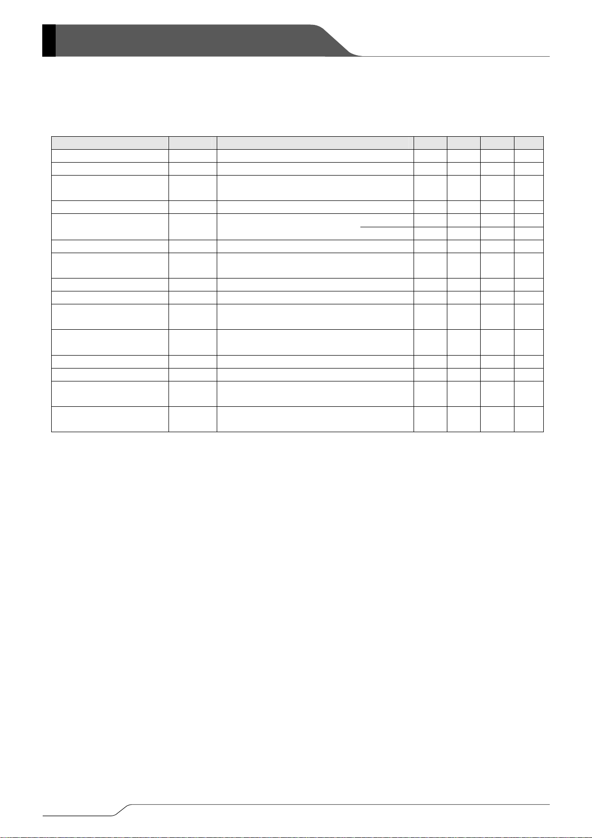
XC6365A503MR, XC6366A503MR
PAR AMETER SYMBOL CONDITIONS MIN. TYP. MAX. UNITS
Output Voltage VOUT 4.875 5.000 5.125 V
Maximum Input Voltage VIN 10.0 - - V
UVLO Voltage
(Minimum Operating Voltage)
VUVLO
Same as IDD1,
Voltage which EXT/pin voltage holding “H” level
Supply Current 1 IDD1 No external components, CE=VDD, VOUT=0V - 67 122
Supply Current 2 IDD2
No external components,
CE=V
OUT=VDD
Stand-by Current ISTB No external components, CE=VOUT=0V - - 0.5
Oscillation Frequency f
OSC
Measuring of EXT/ waveform,
V
IN=output voltage + 0.1V
Maximum Duty Ratio MAXDTY 100 - - %
PFM Duty Ratio PFMDTY No load (XC6366 only) 15 25 35 %
CE "High" Voltage VCEH
CE "Low" Voltage VCEL
No external components, VOUT=0V,
Voltage which EXT/pin voltage holding “L” level
No external components, VOUT=0V,
Voltage which EXT/pin voltage holding “H” level
EXT "High" ON Resistance REXTBH Same as IDD2, VEXT/=VIN-0.4V - 12 17
EXT "Low" ON Resistance REXTBL Same as IDD1, VEXT/=0.4V - 10 14
Efficiency EFFI
Soft-Start Time tSS
Conditions: 1. Unless otherwise stated, connect external components. VIN=VDD = 7.5V, IOUT = 330mA
2. XC6365/66C series external components: C
Use of a XP162A12A6
transistor recommended
Connect R
(When V
SS, CSS, CE, 0V→ 3.0V
IN≦3.0V, VIN=3.0V)
SS=0.033μF, R SS=470kΩ
(VOUT=5.0V, f
XC6365 - 67 122
XC6366 - 16 29
=300kHz)
OSC
Ta =2 5℃
0.9 - 2.2 V
μA
μA
μA
μA
255 300 345 kHz
0.65 - - V
- - 0.20 V
μA
μA
- 93 - %
5 10 20 ms
6/24
Page 7
XC6365/XC6366
Series
■ELECTRICAL CHARACTERISTICS (Continued)
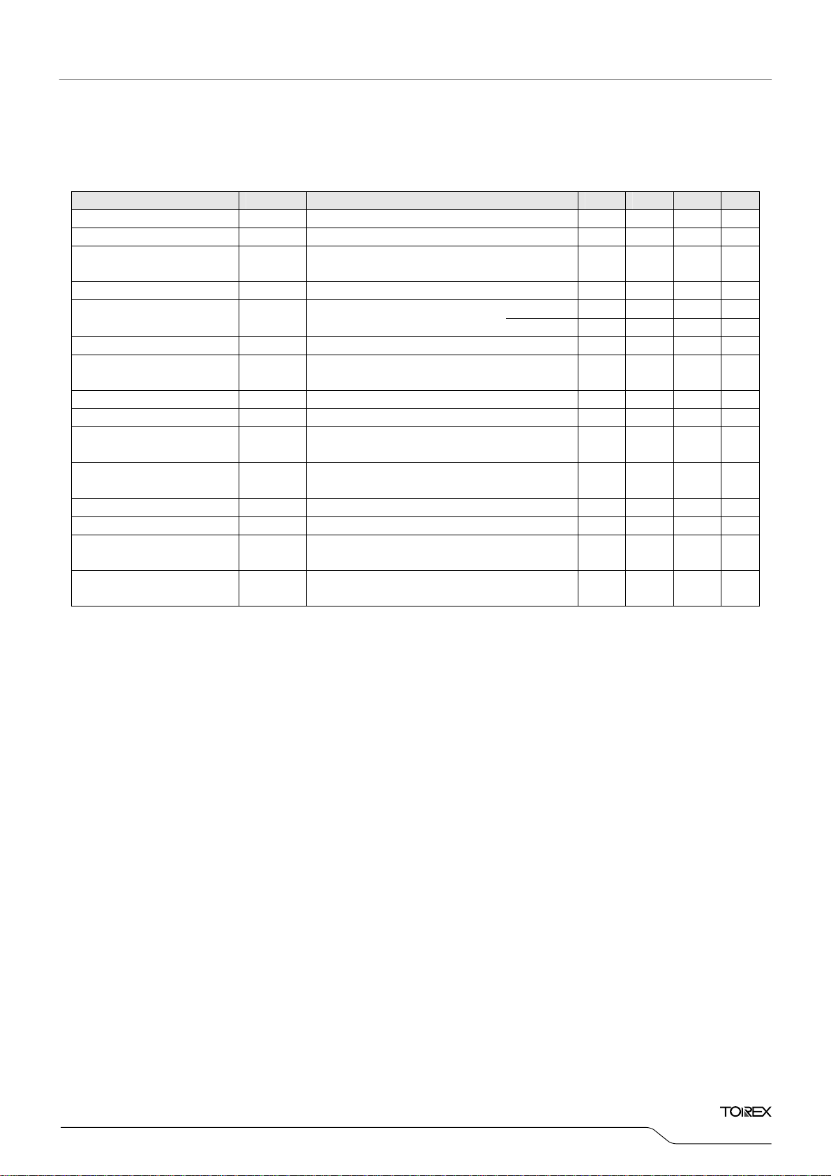
XC6365B103MR, XC6366B103MR
PAR AMETER SYMBOL CONDITIONS MIN. TYP. MAX. UNITS
Output Voltage VOUT 2.925 3.000 3.075 V
Maximum Input Voltage VIN 10.0 - - V
UVLO Voltage
(Minimum Operating Voltage)
VUVLO
Same as IDD1,
Voltage which EXT/pin voltage holding “H” level
Supply Current 1 IDD1 No external components, CE=VIN, VOUT=0V - 55 100
Supply Current 2 IDD2
No external components,
CE=V
DD, FB=1.2V
Stand-by Current ISTB No external components, CE=FB=0V - - 0.5
Oscillation Frequency f
OSC
Measuring of EXT/ waveform,
V
IN=output voltage + 0.1V
Maximum Duty Ratio MAXDTY 100 - - %
PFM Duty Ratio PFMDTY No load (XC6366 only) 15 25 35 %
CE "High" Voltage VCEH
CE "Low" Voltage VCEL
No external components, FB=0V,
Voltage which EXT/pin voltage holding “L” level
No external components, VOUT=0V,
Voltage which EXT/pin voltage holding “H” level
EXT "High" ON Resistance REXTBH Same as IDD2, VEXT/=VIN-0.4V - 17 24
EXT "Low" ON Resistance REXTBL Same as IDD1, VEXT/=0.4V - 15 20
Efficiency EFFI
Soft-Start Time tSS
Conditions: 1. Unless otherwise stated, connect external components. VIN=VDD = 4.5V, IOUT = 200mA
2. XC6365/66C series external components: C
3. R
FB1 = 400kΩ, RFB2 = 200kΩ, CFB = 100ppF
Use of a XP162A12A6
transistor recommended
Connect R
(When V
SS, CSS, CE, 0V→ 3.0V
IN≦3.0V, VIN=3.0V)
SS=0.033μF, R SS=470kΩ
(VOUT=3.0V, f
=300kHz) Ta=25℃
OSC
0.9 - 2.2 V
XC6365 - 55 100
XC6366 - 15 27
255 300 345 kHz
0.65 - - V
- - 0.20 V
- 92 - %
5 10 20 ms
μA
μA
μA
μA
μA
μA
7/24
Page 8

XC6365/XC6366 Series
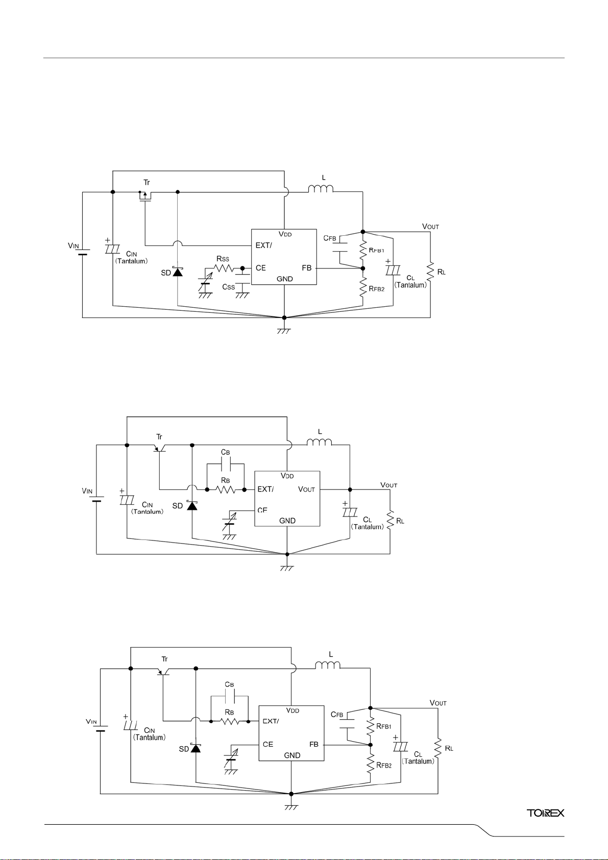
■TEST CIRCUITS
Circuit 1. XC6365A, XC6366A
Circuit 2. XC6365B, XC6366B
Circuit 3. XC6365C, XC6366C
8/24
Page 9
,
)
■TEST CIRCUITS (Continued)
Circuit 4. XC6365D, XC6366D
XC6365/XC6366
Series
Circuit 5. XC6365A
Circuit 6. XC6365B, XC6366B (when used with a PNP transistor)
XC6366A (when used with a PNP transistor
9/24
Page 10
)
XC6365/XC6366 Series
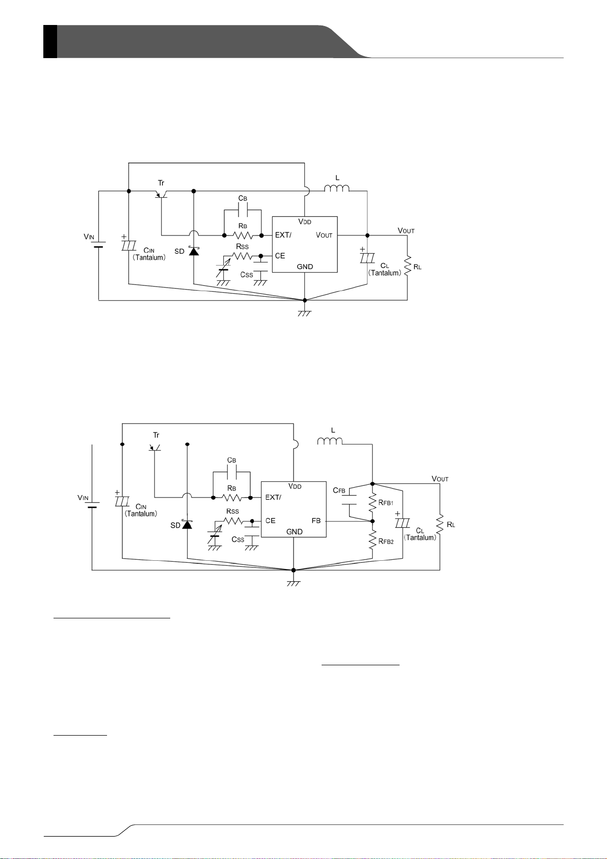
■TEST CIRCUITS (Continued)
Circuit 7. XC6365C, XC6366C (when used with a PNP transistor)
Circuit 8. XC6365D, XC6366D (when used with a PNP transistor
Recommended Components C, D type (soft-start externally set-up)
Tr : XP162A12A6PR (Torex P-channel Power MOSFET) CSS : 0.033μF (Ceramic Capacitor)
Please use a PNP transistor where VIN < 2.5V RSS : 470kΩ(C type), 330kΩ(D type)
L : 22μH (CR54, SUMIDA, f
47μH (CR75, SUMIDA, f
10μH (CR54, SUMIDA, f
SD : MA2Q735 (Schottky Diode, MATSUSHITA) (VOUT = setting output voltage),
CL :10V, 47μF (Tantalum capacitor, NICHICHEMl MCE) RFB1 = RFB2 ≦ 2MΩ
CIN :16V 10μF (Tantalum capacitor, NICHICHEMI MCE) CFB : Set up so that fzfb = 1÷(2π x CFB x RFB1) is within
the 0.5 to 20kHz range (10kHz conventional)
PNP Tr. Type Adjustments necessary in respect of L, CL.
Tr : 2SA1213 (TOSHIBA) e.g. : VOUT = 3.0V
RB : 500Ω(Adjust according to load and Tr. hFE levels) RFB1 = 400kΩ, RFB2 = 200kΩ, CFB = 100pF
CB : 2200pF (Ceramic Type)
Set up so that CB≦1 / (2π x RB x FOSC x 0.7)
=300kHz)
OSC
=180kHz) B, D type (FB type)
OSC
=500kHz) RFB : Set up so that RFB1 / RFB2 = VOUT – 1
OSC
10/24
Page 11
XC6365/XC6366
■NOTES ON USE
1. Take ample care to ensure that none of the IC's, nor the external component's, absolute maximum ratings are exceeded.
2. Be extremely careful when selecting parts and do not limit your reference to the specifications and characteristics for the
DC/DC converter alone. The IC also depends, to a great extent, upon the external components.
3. Arrange the peripherals in the environs of the IC. In order to reduce wiring impedance, use short, thick wires. In particular,
wire the load capacitor as close as possible and strengthen the ground wiring sufficiently.
4. Ground current during switching may cause the IC's operations to become unstable due to changes in ground voltage, so
please strengthen the IC's GND pin surroundings.
●External Components
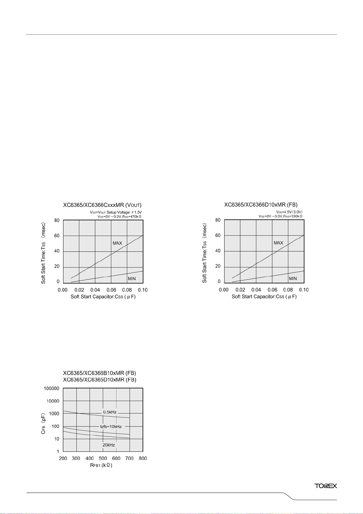
1. Setting soft start time
To set a longer soft start time, please use XC6365C or XC6365D series which soft start function is externally set up.
For the measurement of soft start time TSS, the time is needed to be between the maximum and the minimum value indicated
in the chart below. Please set a soft start capacitor C
SS according to the application.
Series
2. Setting R
fzfb=1 ÷ (2 π × CFB × RFB1)
As the combination of R
fzfb=20kHz as the chart below can be effective.
Under normal condition, please set the combination to configure around fzfb=10kHz.
FB1 and CFB
FB1 and CFB enable to set fzfb between 0.5kHz to 20kHz, within the realm of fzfb=0.5kHz to
11/24
Page 12
XC6365/XC6366 Series
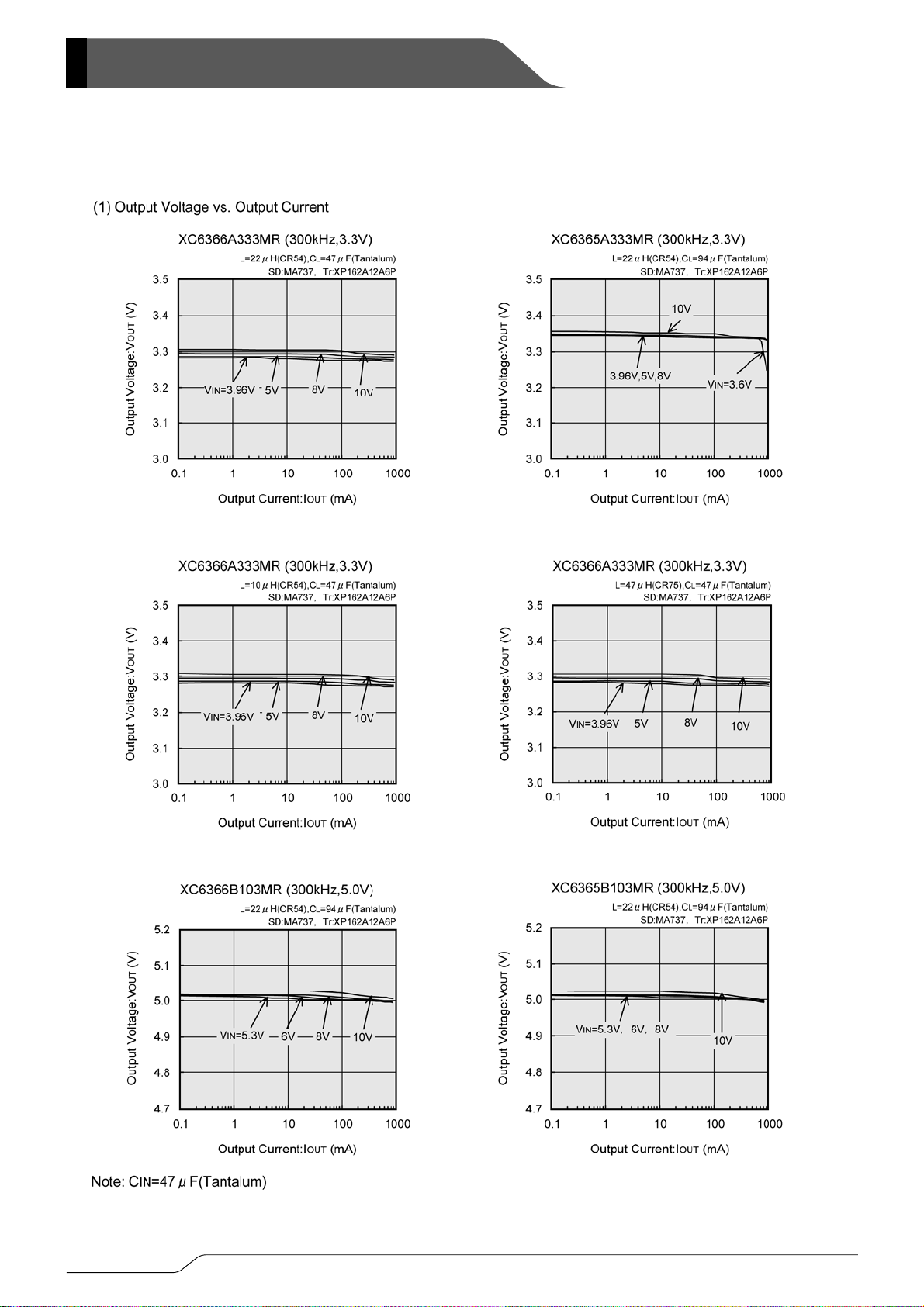
■TYPICAL PERFORMANCE CHARACTERISTICS
12/24
Page 13
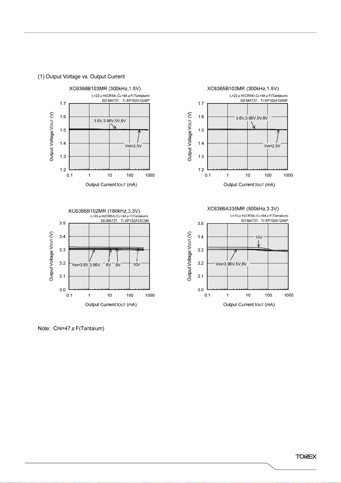
■TYPICAL PERFORMANCE CHARACTERISTICS (Continued)
(Continued)
XC6365/XC6366
Series
13/24
Page 14
XC6365/XC6366 Series
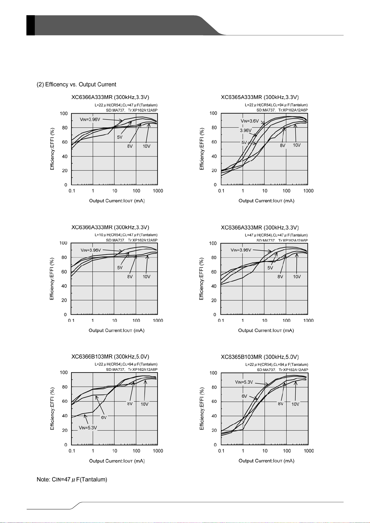
■TYPICAL PERFORMANCE CHARACTERISTICS (Continued)
14/24
Page 15
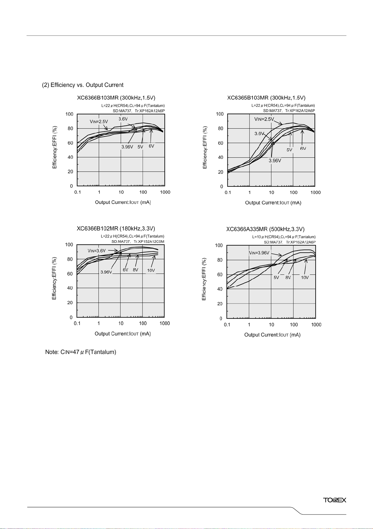
■TYPICAL PERFORMANCE CHARACTERISTICS (Continued)
(Continued)
XC6365/XC6366
Series
15/24
Page 16
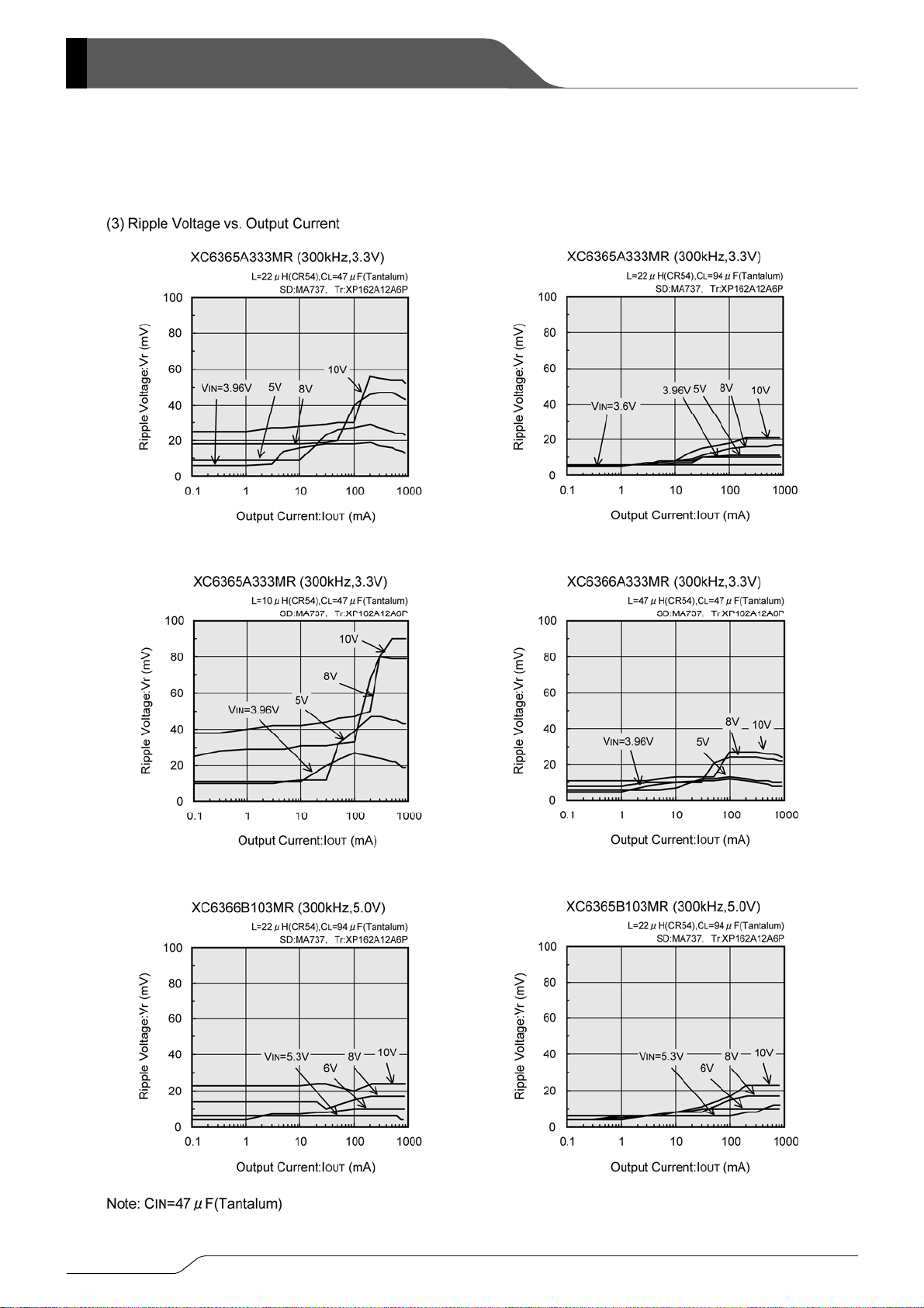
XC6365/XC6366 Series
■TYPICAL PERFORMANCE CHARACTERISTICS (Continued)
16/24
Page 17
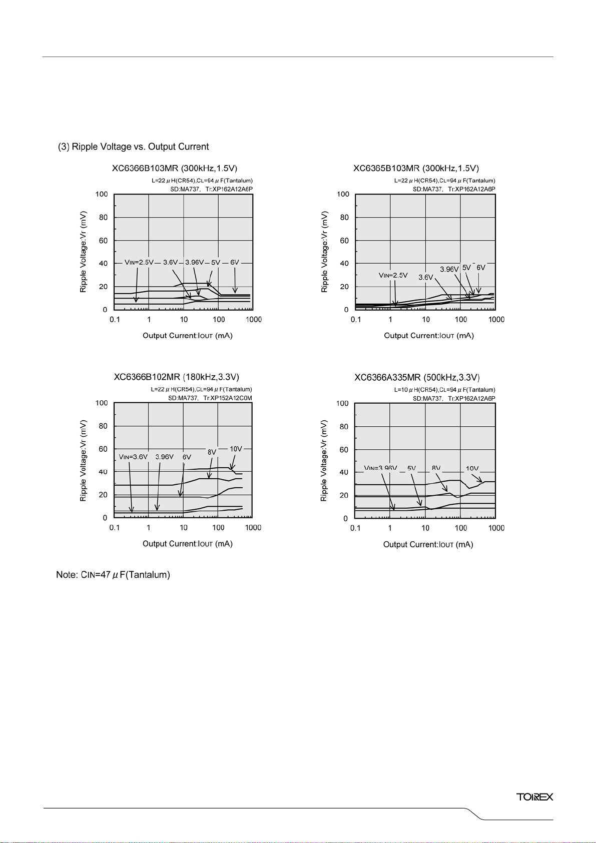
■TYPICAL PERFORMANCE CHARACTERISTICS (Continued)
(Continued)
XC6365/XC6366
Series
17/24
Page 18
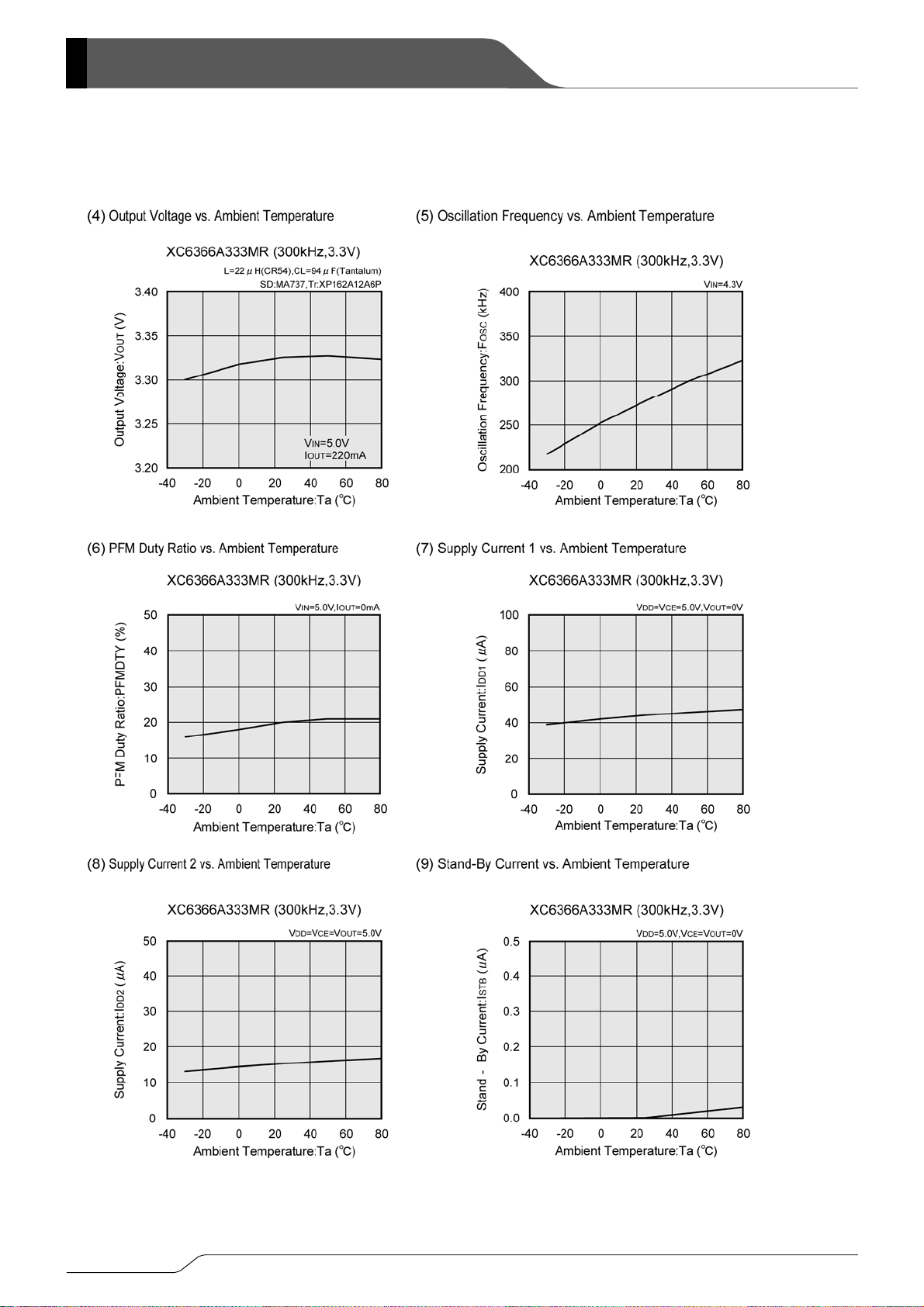
XC6365/XC6366 Series
■TYPICAL PERFORMANCE CHARACTERISTICS (Continued)
18/24
Page 19
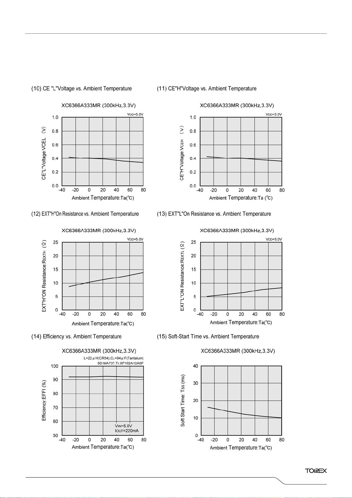
■TYPICAL PERFORMANCE CHARACTERISTICS (Continued)
XC6365/XC6366
Series
19/24
Page 20
XC6365/XC6366 Series
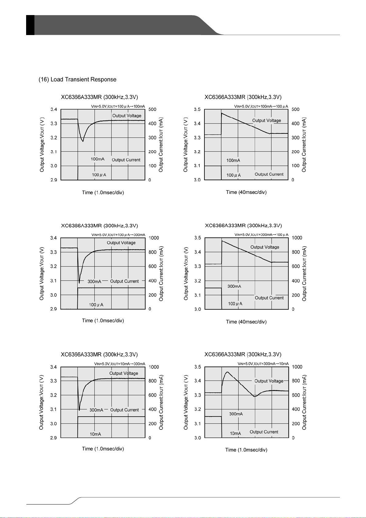
■TYPICAL PERFORMANCE CHARACTERISTICS (Continued)
20/24
Page 21
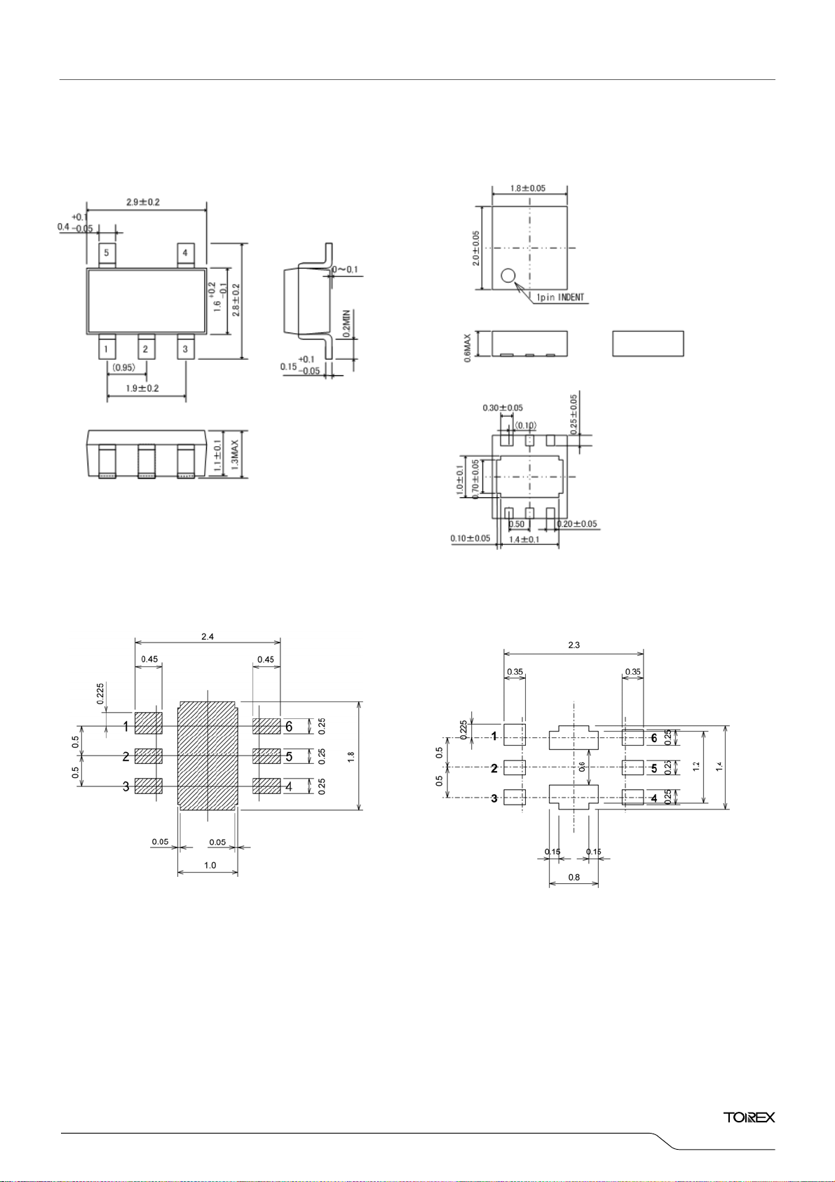
■PACKAGING INFORMATION
●SOT-25
XC6365/XC6366
Series
●USP-6C
●USP-6C Reference Pattern Layout
●USP-6C Reference Metal Mask Design
21/24
Page 22
XC6365/XC6366 Series
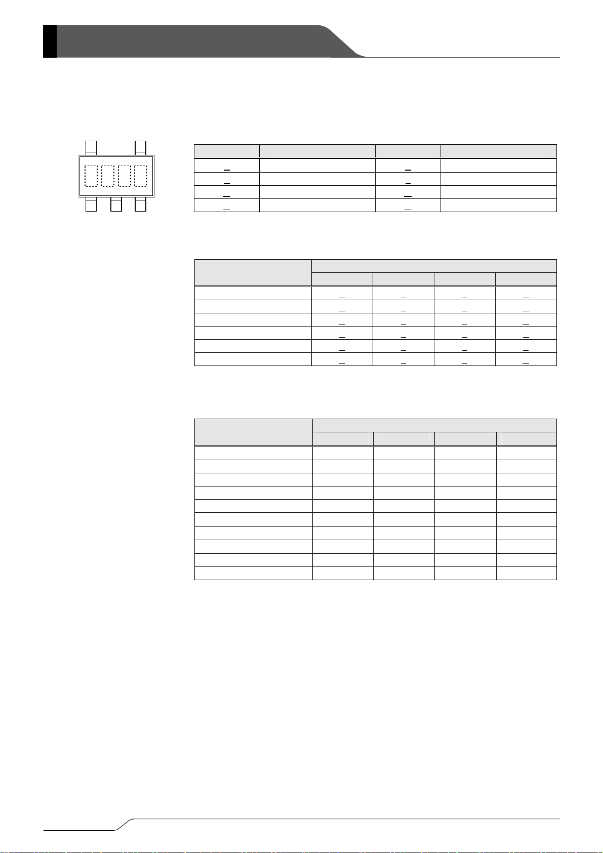
■MARKING RULE
54
① ② ③ ④
123
SOT-25
(TOP VIEW)
① represents product classification
MARK PRODUCT SERIES MARK PRODUCT SERIES
② represents integer of output voltage and oscillation frequency
OUTPUT VOLTAGE
③ represents decimal number of output voltage and oscillation frequency
OUTPUT VOLTAGE
④ represents production lot number
0 to 9, A to Z repeated (G, I, J, O, Q, W excluded)
A XC6365A K XC6366A
B XC6365B L XC6366B
C XC6365C M XC6366C
D XC6365D N XC6366D
OSCILLATION FREQUENCY (kHz)
100 180 300 500
1.x B 1 1 B
2.x C 2 2 C
3.x D 3 3 D
4.x E 4 4 E
5.x F 5 5 F
6.x H 6 6 H
OSCILLATION FREQUENCY (kHz)
100 180 300 500
x.0 0 0 A A
x.1 1 1 B B
x.2 2 2 C C
x.3 3 3 D D
x.4 4 4 E E
x.5 5 5 F F
x.6 6 6 H H
x.7 7 7 K K
x.8 8 8 L L
x.9 9 9 M M
22/24
Page 23
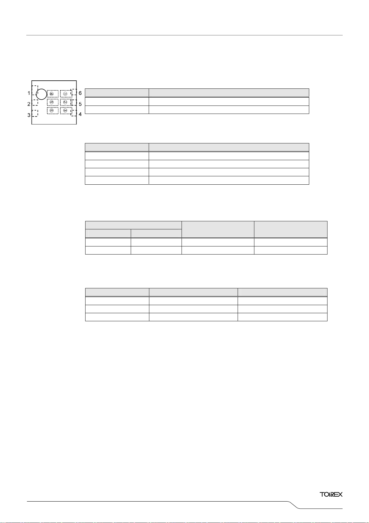
■MARKING RULE (Continued)
USP-6C
(TOP VIEW)
① represents product series
MARK PRODUCT SERIES
2 XC6365****E*
0 XC6366****E*
② represents product classification
MARK PRODUCT SERIES
A XC6365/66A***E*
B XC6365/66B***E*
C XC6365/66C***E*
D XC6365/66D***E*
③④ represents output voltage
e.g.:
MARK
③ ④
3 3 3.3 XC6365/66*33*E*
5 0 5.0 XC6365/66*50*E*
represents oscillation frequency
⑤
MARK
2 180kHz XC6365/66***2E*
3 300kHz XC6365/66***3E*
5 500kHz XC6365/66***5E*
represents production lot number
⑥
0 to 9, A to Z repeated (G, I, J, O, Q, W excluded)
OUTPUT VOLTAGE (V)
OCSILLATION FREQUENCY
XC6365/XC6366
Series
PRODUCT SERIES
PRODUCT SERIES
23/24
Page 24
XC6365/XC6366 Series
1. The products and product specifications contained herein are subject to change without
notice to improve performance characteristics. Consult us, or our representatives
before use, to confirm that the information in this datasheet is up to date.
2. We assume no responsibility for any infringement of patents, patent rights, or other
rights arising from the use of any information and circuitry in this datasheet.
3. Please ensure suitable shipping controls (including fail-safe designs and aging
protection) are in force for equipment employing products listed in this datasheet.
4. The products in this datasheet are not developed, designed, or approved for use with
such equipment whose failure of malfunction can be reasonably expected to directly
endanger the life of, or cause significant injury to, the user.
(e.g. Atomic energy; aerospace; transport; combustion and associated safety
equipment thereof.)
5. Please use the products listed in this datasheet within the specified ranges.
Should you wish to use the products under conditions exceeding the specifications,
please consult us or our representatives.
6. We assume no responsibility for damage or loss due to abnormal use.
7. All rights reserved. No part of this datasheet may be copied or reproduced without the
prior permission of TOREX SEMICONDUCTOR LTD.
24/24
 Loading...