

XC6601 Series
ETR0335_006
Low Voltage Input LDO Voltage Regulator with Soft-Start Function
■GENERAL DESCRIPTION
The XC6601 series is a low voltage input CMOS LDO regulator which provides highly accurate (±20mV) outputs and can
supply current efficiently due to its ultra low on-resistance even at low output voltages. The series is ideally suited to the
applications which require very low dropout voltage operation and consists of a voltage reference, an error amplifier, a driver
transistor, a current limiter, a fold back circuit, a thermal shutdown (TSD) circuit, an under voltage lock out (UVLO) circuit,
soft-start circuit and a phase compensation circuit.
Output voltage is selectable in 0.05V increments within a range of 0.7V to 1.8V using laser trimming technology and ceramic
capacitors can be used for the output stabilization capacitor (C
The over current protection circuit (the current limiter and the fold back circuit) as well as the thermal shutdown circuit (the
TSD circuit) are built-in. These two protection circuits will operate when either the output current reaches the current limit
level or the junction temperature reaches the temperature limit level.
With the built-in UVLO function, the regulator output is forced OFF when the voltage level at the V
below the UVLO voltage level. With the soft-start function, the inrush current from V
be reduced and makes the V
The CE function enables the output to be turned off and the series to be put in stand-by mode resulting in greatly reduced
power consumption. At the time of entering the stand-by mode, the series enables the electric charge at the output capacitor
(C
) to be discharged via the internal auto-discharge switch which is located between the V
L
result the V
■APPLICATIONS
●Mobile phones
●Cordless phones
●Wireless communication equipment
●Portable games
●Cameras
●Audio visual equipment
●Portable AV equipment
●PDAs
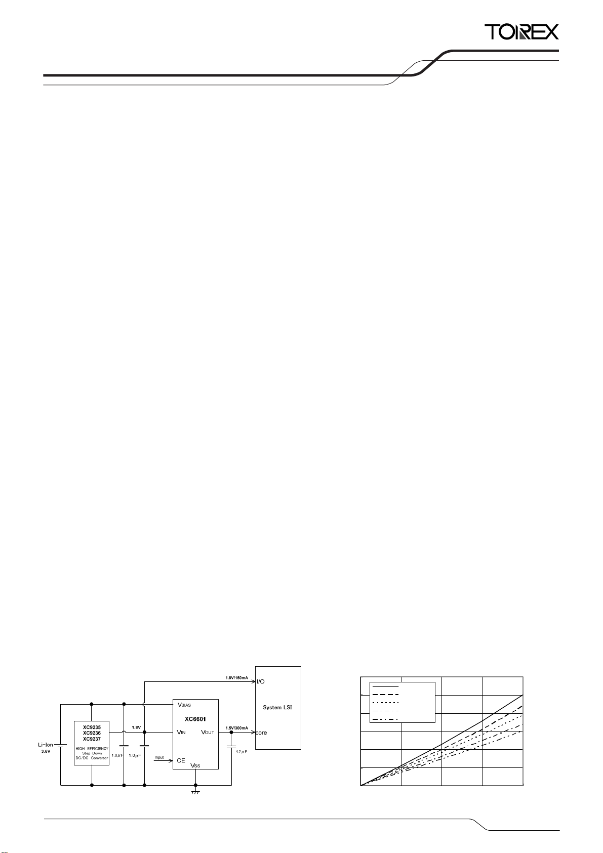
■ TYPICAL APPLICATION CIRCUIT
●VBIAS =3.6V , VIN =1.8V , VOUT =1.5V
pin quickly returns to the VSS level.
OUT
stable.
IN
).
L
BIAS pin or the VIN pin falls
IN
to V
for charging CL at start-up can
OUT
pin and the VSS pin. As a
OUT
■FEATURES
Maximum Output Current
Dropout Voltage
Bias Voltage Range
Input Voltage Range
: 400mA
: 38mV@I
(at V
: 2.5V ~ 6.0V (VBIAS - VOUT≧1.2V)
: 1.0V ~ 3.0V(V
Output Voltage Range : 0.7V ~ 1.8V (0.05V increments)
Output Voltage Accuracy :±20mV
Power Consumption : IBIAS=25μA , I IN=1.0μA
BIAS=0.01μA , I IN=0.01μA
I
UVLO : VBIAS=2.0V, VIN=0.4V (TYP.)
TSD (Detect/Release) : 150℃/125℃ (TYP.)
Soft-Start Time : 240μs @ V
Operating Temperature Range
Function
Low ESR Capacitor
: -40℃ ~ +85℃
: C
: Ceramic Capacitor Compatible
Packages : USP-6C, SOT-25, SOT-89-5
Environmentally Friendly
: EU RoHS Compliant, Pb Free
(Limit:550mA TYP.)
OUT=100mA (TYP.)
BIAS - VOUT=2.4V)
IN≦VBIAS)
=1.2V (TYP.)
OUT
L High Speed Auto-Discharge
■ TYPICAL PEFORMANCE
CHARACTERISTICS
●Dropout Voltage vs. Output Current
XC6601B121MR
300
250
200
150
100
Dropout Volt age: Vdif(mV)
50
0
0 100 200 300 400
VBIAS=3.0V
VBIAS=3.3V
VBIAS=3.6V
VBIAS=4.2V
VBIAS=5.0V
Out put Curr ent: I OUT(mA )
Ta=25 [℃]
(TYP.)
(TYP.)
1/33
XC6601 Series
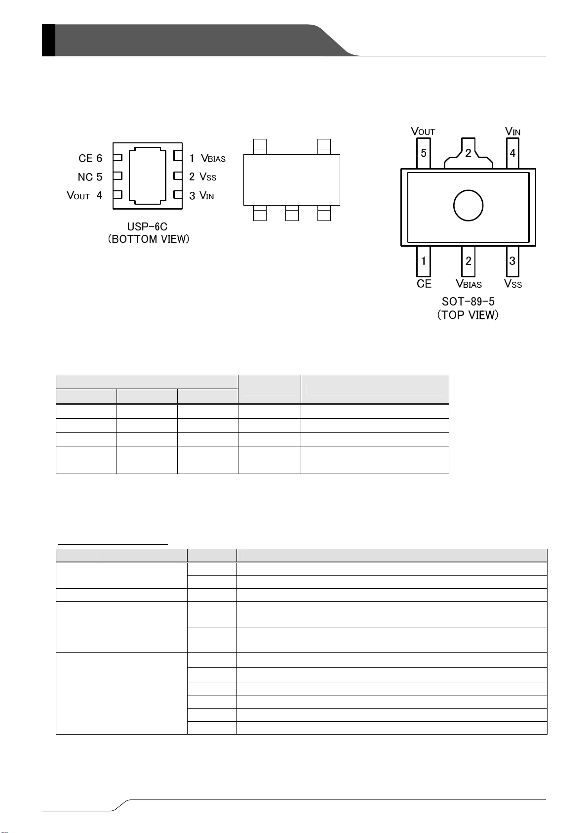
■PIN CONFIGURATION
●USP-6C ●SOT-25 ●SOT-89-5
123
*The heat dissipation pad of the USP-6C
package is recommended to solder as the
recommended mount pattern and metal
mask pattern for mounting strength. This
pad should be electrically opened or
connected to the V
■PIN ASSIGNMENT
BIAS (No.1) pin.
PIN NUMBER
USP-6C SOT-25 SOT-89-5
SOT-25
(TOP VIEW)
PIN NAME FUNCTION
1 2 2 VBIAS Power Supply Input
3 1 4 VIN Driver Transistor Input
4 5 5 VOUT Output
2 3 3 VSS Ground
6 4 1 CE ON/OFF Control
■PRODUCT CLASSIFICATION
●Ordering Information
XC6601①②③④⑤⑥-⑦
(*1)
: CE High Active, Soft-Start Function Built-in, CL Auto Discharge Function
MARK DESCRIPTION SYMBOL DESCRIPTION
①
②③
④
Type of Regulators
Output Voltage 07 ~ 18
Output Voltage
Type
A Pull-Down Resistor Built-in
B No Pull-Down Resistor Built-in
e.g.) VOUT(T)=1.2V⇒②=1,③=2
1
B
0.1V increments
e.g.) 1.2V⇒②=1,③=2,④=1
0.05V increments
e.g.) 1.25V⇒②=1,③=2,④=B
MR SOT-25
MR-G SOT-25
⑤⑥-⑦
Packages
Taping Type
(*2)
ER USP-6C
ER-G USP-6C
PR SOT-89-5
PR-G SOT-89-5
(*1)
The ”-G” suffix indicates that the products are Halogen and Antimony free as well as being fully RoHS compliant.
(*2)
The device orientation is fixed in its embossed tape pocket.
For reverse orientation, please contact your local Torex sales office or representative.
(Standard orientation: ⑤R-⑦, Reverse orientation: ⑤L-⑦)
2/33
CEVOUT
45
VSSVBIASVIN
(1)
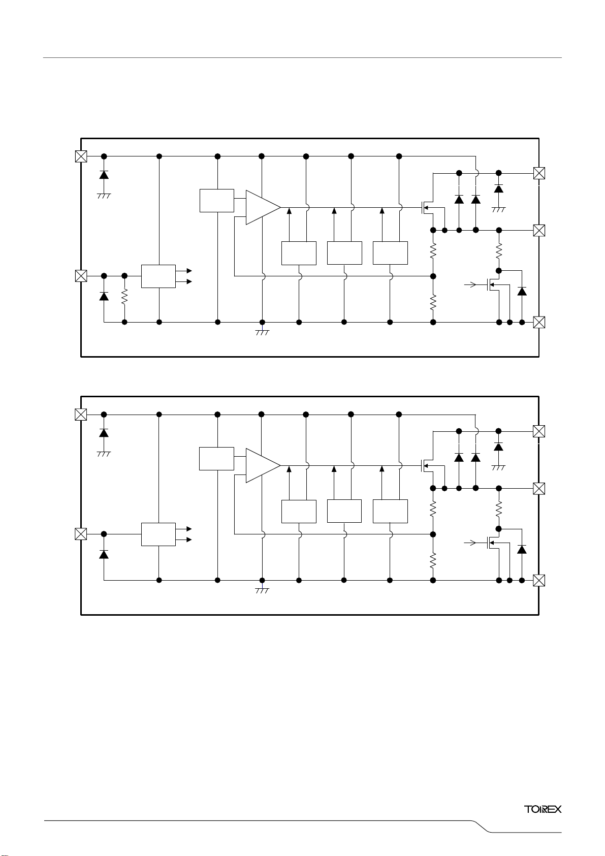
■BLOCK DIAGRAMS
XC6601A Series
(1)XC6601A Series
V
BIAS
Voltage Reference
With
Soft Start
+
Error
Amp
-
Control
CE/
each
circuit
CE
CE
ON/OFF
R pull-down
Under Voltage
Lock Out
(2) XC6601B Series
(2)XC6601B Series
V
BIAS
Voltage Reference
With
Soft Start
+
Error
Amp
-
CE
ON/OFF
Control
CE/
each
circuit
CE
Under Voltage
Lock Out
*Diodes inside the circuit are an ESD protection diode and a parasitic diode.
Thermal
Protection
Thermal
Protection
Current
Limit
Current
Limit
XC6601
Series
V
IN
V
OUT
CE/
CE/
Rdischg
Rdischg
V
SS
V
IN
V
OUT
V
SS
R1
R2
R1
R2
3/33
XC6601 Series
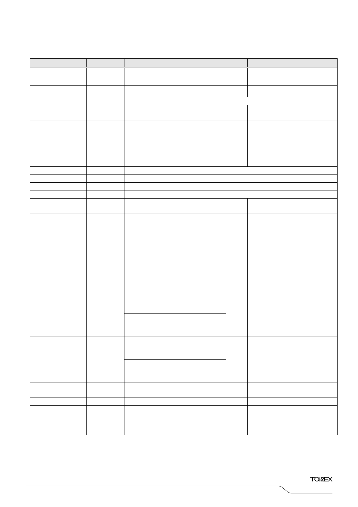
■MAXIMUM ABSOLUTE RATINGS
PAR AMETER SYMBOL RATINGS UNITS
Bias Voltage VBIAS VSS-0.3 ~ +7.0 V
Input Voltage VIN VSS-0.3 ~ +7.0 V
Output Current IOUT 700
Output Voltage VOUT
VSS-0.3 ~ VBIAS+0.3
VSS-0.3 ~ VIN+0.3
(*1)
mA
CE Input Voltage VCE VSS-0.3 ~ +7.0 V
100
250
500
Power Dissipation
USP-6C
SOT-25
SOT-89-5
Pd
1000 (PCB mounted) *2
600 (PCB mounted) *2
1300 (PCB mounted) *2
Operating Temperature Range Topr -40 ~ +85 ℃
Storage Temperature Range Tstg -55 ~ +125 ℃
(*1)
IOUT=Less than Pd / (VIN-VOUT)
(*2)
The power dissipation figure shown is PCB mounted. Please refer to pages 29~31 for details.
4/33
Ta =2 5 ℃
V
mW
■ELECTRICAL CHARACTERISTICS
XC6601
Series
Ta =2 5 ℃
PAR AMETER SYMBOL CONDITIONS MIN. TYP. MAX. UNITS
Bias Voltage
Input Voltage
Output Voltage VOUT(E)
Maximum Output
Current 1
Maximum Output
Current 2
Maximum Output
Current 3
Load Regulation
Dropout Voltage 1 Vdif1
Dropout Voltage 2 Vdif2
Dropout Voltage 3 Vdif3
Dropout Voltage 4 Vdif4
Supply Current 1 IBIAS
Supply Current 2 IIN
Bias Current
Stand-by Current 1 IBIAS_STB
Stand-by Current 2 IIN_STB
Bias Regulation
(*1)
V
(*2)
V
BIAS
IN
IOUTMAX 1
IOUTMAX 2
IOUTMAX 3
OUT
△V
(*10)
IBIASMAX
△V
OUT/
(△V
BIAS・VOUT)
(*7)
(*7)
(*7)
(*7)
(*3)
VCE =V
V
VBIAS=VCE=3.6V, VIN =VOUT(T)+0.3V,
V
CE =VBIAS
V
V
CE =VBIAS
V
V
CE =VBIAS
V
V
BIAS=VCE=3.6V, VIN=VOUT(T)+0.3V,
1mA≦I
BIAS=VCE, IOUT=100mA E-1
V
V
CE =VBIAS
V
CE =VBIAS
V
CE =VBIAS
=V
BIAS,VIN
BIAS=VCE
=3.6V
IOUT=100mA
,V
BIAS -VOUT(T)
=V
IN
,V
=V
IN
,V
=V
IN
+0.5V
OUT(T)
BIAS -VOUT(T)
+0.5V
OUT(T)
BIAS -VOUT(T)
+0.5V
OUT(T)
OUT≦300mA
, I
OUT
, I
OUT
, I
OUT
VBIAS=VCE=3.6V, VIN=VOUT(T)+0.3V
V
OUT=OPEN
VBIAS=VCE=3.6V, VIN=VOUT(T)+0.3V
V
OUT=OPEN
V
≧1.0V
OUT(T)
V
BIAS=VCE
V
V
= V
OUT
V
OUT(T)
BIAS=VCE
V
= V
OUT
=3.6V, VIN=V
OUT(T)
<1.0V
=3.6V, VIN=1.0V
OUT(T)
VBIAS=6.0V, VIN=3.0V, VCE=VSS - 0.01 0.10
VBIAS=6.0V, VIN=3.0V, VCE=VSS - 0.01 0.35
V
≧1.3V
OUT(T)
V
+1.2V≦V
V
IN=VOUT(T)
V
IN=VOUT(T)
OUT(T)
+0.3V, V
2.5V≦V
+0.3V, V
V
OUT(T)
BIAS
CE =VBIAS
<1.3V
≦6.0V,
BIAS
CE =VBIAS
OUT(T)
+0.3V
2.5 - 6.0 V
1.0 - 3.0 V
-0.02 VOUT(T)
E-0
≧1.2V
≧1.3V
≧1.5V
200 - -
300 - -
400 - -
- 8 17
=200mA E-2
=300mA E-3
=400mA E-4
8 25 45
0.1 1.0 3.0
OUT(T)
- 0.05V
- 1.0 2.5
- 0.05V
≦6.0V,
, I
=1mA
, I
OUT
OUT
=1mA
- 0.01 0.3
(*5)
(*6)
(*6)
(*6)
(*6)
(*4)
+0.02
VOUT(T)≧0.90V,
V
+0.1V≦VIN≦3.0V,
OUT(T)
BIAS=VCE=3.6V, IOUT=1mA
Input Regulation
△V
(△V
OUT/
IN・VOUT)
V
V
OUT(T)<0.90V,
- 0.01 0.1
1.0V≦VIN≦3.0V
BIAS=VCE=3.6V, IOUT=1mA
V
V
Bias Voltage UVLO VBIAS_UVLO
Input Voltage UVLO VIN_UVLO VBIAS=VCE=3.6V, IOUT=1mA
VBIAS Ripple Rejection VBIAS_PSRR
VIN Ripple Rejection VIN_PSRR
CE =VBIAS, VIN =VOUT(T)+0.3V,
OUT=1mA
I
BIAS= V
V
=3.6VDC+0.2Vp-pAC,
CE
VIN=VOUT(T)+0.3V, IOUT=30mA,f=1kHz
VIN=VOUT(T)+0.3VDC+0.2Vp-pAC,
VBIAS=3.6V, IOUT=30mA, f=1kHz
1.37 2.0 2.5
0.07 0.4 0.6
- 40 -
- 60 -
CIRCUIT
①
①
V ①
mA
mA
mA
mV
mV
mV
mV
mV
①
①
①
①
①
①
①
①
μA ①
μA ①
mA
①
μA ①
μA ①
%/V
%/V
V
V
dB
dB
①
①
①
①
②
②
5/33
XC6601 Series
■ELECTRICAL CHARACTERISTICS (Continued)
PAR AMETER SYNBOL CONDITIONS MIN. TYP. MAX. UNITS
Output Voltage
Temperature
Characteristics
Limit Current I
Short Current I
Thermal Shutdown
Detect Temperature
Thermal Shutdown
Release Temperature
△V
OUT/
△Topr・V
LIM
SHORT
TTSD
TTSR
OUT
Hysteresis Width TTSD-TTSR
CL Auto-Discharge
Resistance
Rdischg
CE "H" Level Voltage VCEH VBIAS=3.6V, VIN= VOUT(T)+0.3V 0.75 - 6.0
CE "L" Level Voltage VCEL VBIAS=3.6V, VIN= VOUT(T)+0.3V - - 0.16
CE "H" Level Current
(A Series)
CE "H" Level Current
ICEH
(B Series)
CE "L" Level Current ICEL
IN1
(*11)
t
(*8)
(*9)
-VOUT1
BIAS
}.
≧3.0V is input to the VIN pin.
SS
within the range V
BIAS
within the range VIN≦V
IN
reaches V
OUT
OUTPUT VOLTAGE (V) OUTPUT VOLTAGE (V)
VOUT
BIAS
E-0 E-0
Soft-Start Time
NOTE:
* 1: Please use Bias voltage V
* 2: Please use Input voltage V
* 3: V
OUT(E) = Effective output voltage (Refer to the voltage chart E-0 and E-1)
* 4: V
OUT (T) = Specified output voltage
* 5: E-0 = Please refer to the table named OUTPUT VOLTAGE CHART
* 6: E-1 = Please refer to the table named DROPOUT VOLTAGE CHART
* 7: Vdif = {V
* 8: V
IN1 = The input voltage when VOUT1 appears as input voltage is gradually decreased.
* 9: V
OUT1 = A voltage equal to 98% of the output voltage while maintaining an amply stabilized output voltage when V
V
=3.0V at V
IN
* 10:
IBIASMAX = A supply current at the V
* 11: t
is defined as a time V
SS
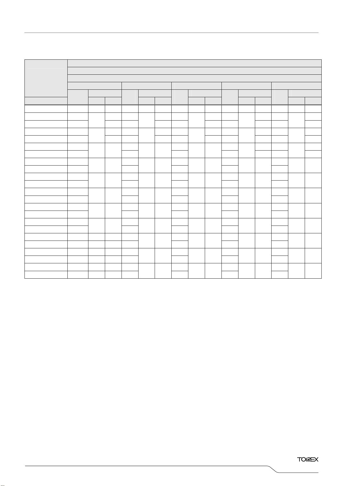
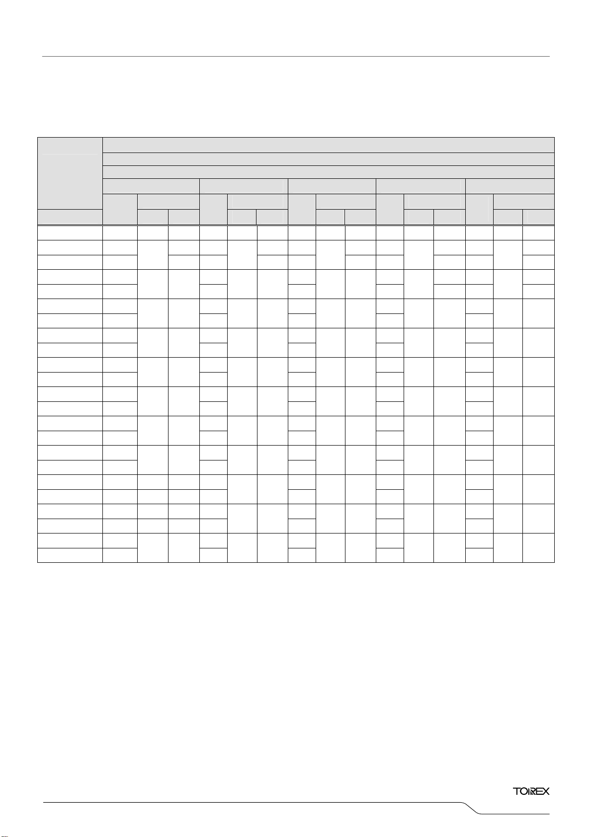
■OUTPUT VOLTAGE CHART
NOMINAL
OUTPUT
VOLTAGE (V)
VOUT(T) MIN. MAX. VOUT(T) MIN. MAX.
0.70 0.680 0.720 1.30 1.280 1.320
0.75 0.730 0.770 1.35 1.330 1.370
0.80 0.780 0.820 1.40 1.380 1.420
0.85 0.830 0.870 1.45 1.430 1.470
0.90 0.880 0.920 1.50 1.480 1.520
0.95 0.930 0.970 1.55 1.530 1.570
1.00 0.980 1.020 1.60 1.580 1.620
1.05 1.030 1.070 1.65 1.630 1.670
1.10 1.080 1.120 1.70 1.680 1.720
1.15 1.130 1.170 1.75 1.730 1.770
1.20 1.180 1.220 1.80 1.780 1.820
1.25 1.230 1.270
BIAS=VCE=3.6V, VIN=VOUT(T)+0.3V ,
V
I
OUT=30mA,
- ±100 -
- 40℃≦ Topr ≦85℃
OUT=VOUT(E)×0.95,
V
BIAS=VCE=3.6V, VIN=VOUT(T)+0.3V
V
VBIAS=VCE=3.6V, VIN=VOUT(T)+0.3V,
V
OUT=0V
400 550 -
- 80 -
Junction Temperature - 150 -
Junction Temperature - 125 -
- 25 -
V
BIAS=3.6V, VIN= VOUT(T)+0.3V,
V
CE= VSS, VOUT=VOUT(T)
V
BIAS=VCE=6.0V,
V
IN=VOUT(T)+0.3V
VBIAS=6.0V, VCE=VSS
V
IN=VOUT(T)+0.3V
V
=3.6V, VIN=V
BIAS
V
CE
BIAS
(*3)
BIAS –VOUT(E)
pin providing for the output current (I
x0.9V from the time when CE H threshold 0.75V is input to the CE pin.
OUT(E)
+0.3V, I
OUT(T)
=0V→3.6V
≧1.2V
OUT
OUT
=1mA
).
290 430 610 Ω ①
2.4 - 8.0
-0.1 - 0.1
-0.1 - 0.1
100 - 410
NOMINAL
OUTPUT
VOLTAGE (V)
IN
=V
BIAS
VOUT
Ta =2 5 ℃
CIRCUIT
ppm/℃ ①
mA
mA
℃ ①
℃ ①
℃ ①
V
V
μA ①
μA ①
μs ③
at
V
<3.0V, and
BIAS
①
①
①
①
6/33
XC6601
Series
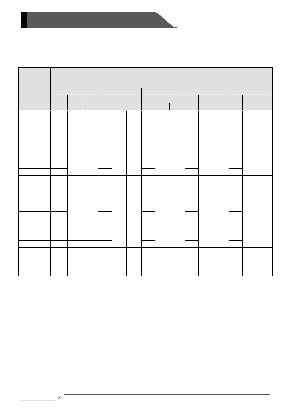
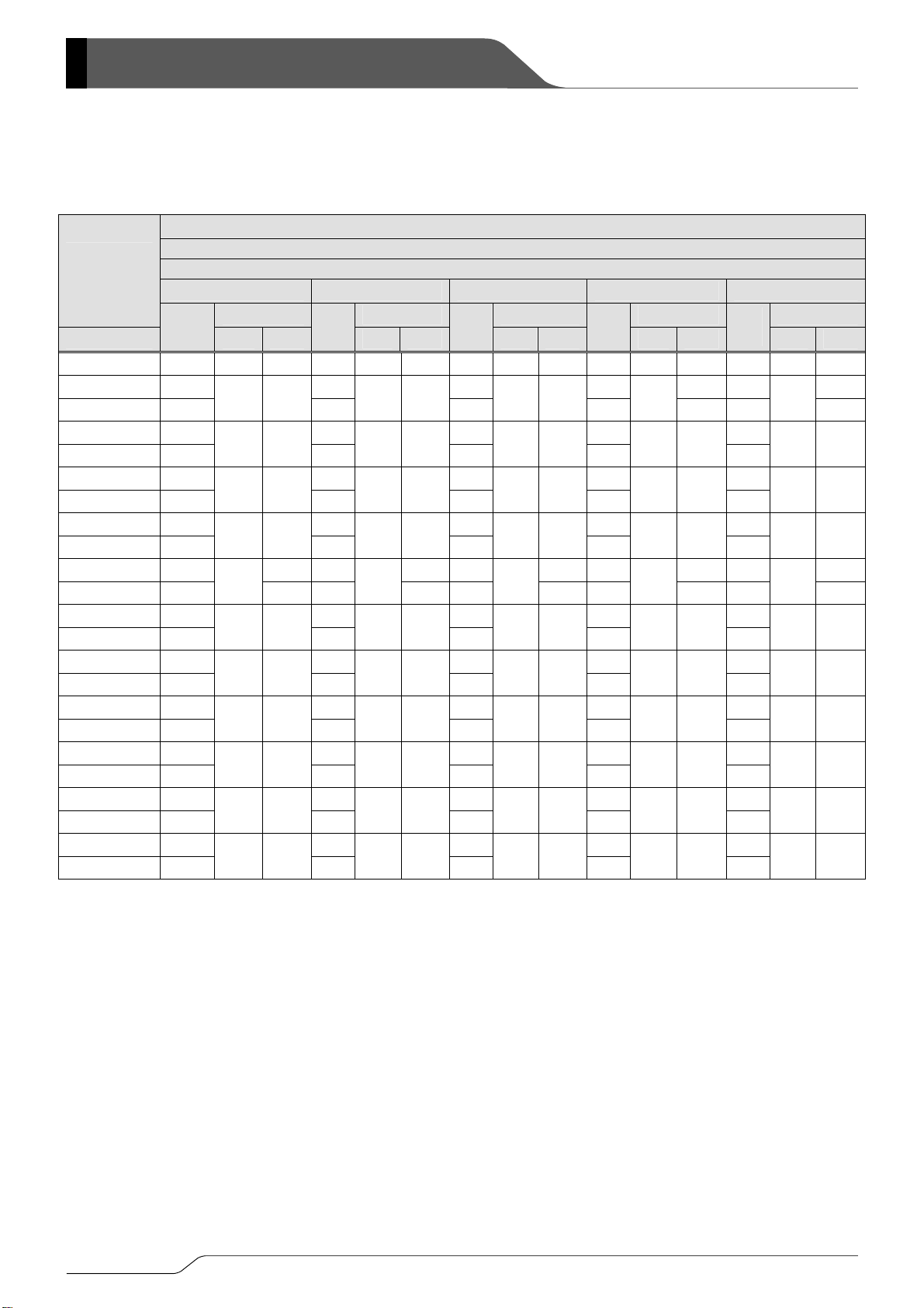
■DROPOUT VOLTAGE CHART
E-1
NOMINAL
OUTPUT
VOLTAGE (V)
VOUT(T)
VBIAS=3.0 (V) VBIAS=3.3 (V) VBIAS=3.6 (V) VBIAS=4.2 (V) VBIAS=5.0 (V)
(*1)
Vgs
(V)
Vdif(mV) Vdif(mV) Vdif(mV) Vdif(mV) Vdif(mV)
TYP. MAX.
Vgs
(V)
TYP. MAX.
0.70 2.30 40 300 2.60 35 300 2.90 33 300 3.50 30 300 4.30 27 300
0.75 2.25 250 2.55 250 2.85 250 3.45 250 4.25 250
0.80 2.20
0.85 2.15 150 2.45 150 2.75 150 3.35 150 4.15 150
0.90 2.10
0.95 2.05 2.35 2.65 3.25 50 4.05 50
1.00 2.00
1.05 1.95 2.25 2.55 3.15 3.95
1.10 1.90
1.15 1.85 2.15 2.45 3.05 3.85
1.20 1.80
1.25 1.75 2.05 2.35 2.95 3.75
1.30 1.70
1.35 1.65 1.95 2.25 2.85 3.65
1.40 1.60
1.45 1.55 1.85 2.15 2.75 3.55
1.50 1.50
41
200 2.50
42
100 2.40
43 68
46 72
48 75
51 81
54 87
57 92
2.30
2.20
2.10
2.00
1.90
1.80
1.55 1.45 61 94 1.75 2.05 2.65 3.45
1.60 1.40 63 97 1.70
1.65 1.35 67 104 1.65 1.95 2.55 3.35
1.70 1.30 70 113 1.60
1.75 1.25 74 131 1.55 1.85 2.45 3.25
1.80 1.20 79 154 1.50
*1): Vgs is a Gate –Source voltage of the driver transistor that is defined as the value of VBIAS - VOUT (T).
DROPOUT VOLTAGE 1 (mV)
Vdif 1
Vgs
(V)
TYP. MAX.
36
200 2.80
38
100 2.70
40 61
41 63
42 65
43 68
46 72
48 75
51 81
54 87
57 92
2.60
2.50
2.40
2.30
2.20
2.10
2.00
1.90
1.80
34
200 3.40
34
100 3.30
35 56
36 58
38 59
40 61
41 63
42 65
43 68
46 72
48 75
Vgs
(V)
3.20
3.10
3.00
2.90
2.80
2.70
2.60
2.50
2.40
TYP. MAX.
31
200 4.20
31
100 4.10
32
49 4.00
32 50
32 51
33 52
34 53
34 54
35 56
36 58
38 59
Vgs
(V)
3.90
3.80
3.70
3.60
3.50
3.40
3.30
3.20
TYP. MAX.
28
28
28
29 45
29 46
29 47
30 47
30 48
31 48
31 49
32 49
200
100
44
7/33
XC6601 Series
■DROPOUT VOLTAGE CHART (Continued)
E-2
NOMINAL
OUTPUT
VOLTAGE (V)
V
OUT (T)
Vgs
(V)
V
=3.0(V) V
BIAS
(*1)
Vdif(mV) Vdif(mV) Vdif(mV) Vdif(mV) Vdif(mV)
TYP. MAX.
Vgs
(V)
BIAS
TYP. MAX.
0.70 2.30 81 300 2.60 74 300 2.90 68 300 3.50 62 300 4.30 57 300
0.75 2.25 250 2.55 250 2.85 250 3.45 250 4.25 250
0.80 2.20
0.85 2.15 150 2.45 150 2.75 150 3.35 150 4.15 150
0.90 2.10
0.95 2.05 2.35 2.65 3.25 4.05
1.00 2.00
1.05 1.95 2.25 2.55 3.15 3.95
1.10 1.90
1.15 1.85 2.15 2.45 3.05 3.85
1.20 1.80
1.25 1.75 2.05 2.35 2.95 3.75
1.30 1.70
1.35 1.65 1.95 2.25 2.85 3.65
1.40 1.60
1.45 1.55 1.85 2.15 2.75 3.55
1.50 1.50
1.55 1.45 129 197 1.75 2.05 2.65 3.45
1.60 1.40 135 206 1.70
1.65 1.35 145 223 1.65 1.95 2.55 3.35
1.70 1.30 154 248 1.60
1.75 1.25 165 293 1.55 1.85 2.45 3.25
1.80 1.20 175 353 1.50
85
200 2.50
88
131 2.40
90 139
96 146
101 154
108 170
115 179
122 192
2.30
2.20
2.10
2.00
1.90
1.80
76
78
81 123
85 127
88 131
90 139
96 146
101 154
108 170
115 179
122 192
*1): Vgs is a Gate –Source voltage of the driver transistor that is defined as the value of VBIAS - VOUT (T).
8/33
DROPOUT VOLTAGE 2 (mV)
Vdif 2
=3.3(V) V
=3.6(V) V
BIAS
Vgs
(V)
TYP. MAX.
200 2.80
117 2.70
2.60
2.50
2.40
2.30
2.20
2.10
2.00
1.90
1.80
70
200 3.40
72
110 3.3 0
74 111
76 114
78 117
81 123
85 127
88 131
90 139
96 146
101 154
Vgs
(V)
3.20
3.10
3.00
2.90
2.80
2.70
2.60
2.50
2.40
=4.2(V) V
BIAS
TYP. MAX.
63
200 4.20
63
100 4.10
64 98
65 101
67 103
68 106
70 108
72 110
74 111
76 114
78 117
Vgs
(V)
4.00
3.90
3.80
3.70
3.60
3.50
3.40
3.30
3.20
BIAS
=5.0(V)
TYP. MAX.
58
200
58
100
58 88
59 90
59 91
60 92
61 93
62 94
63 95
63 97
64 98
■DROPOUT VOLTAGE CHART (Continued)
E-3
NOMINAL
OUTPUT
VOLTAGE (V)
V
OUT (T)
Vgs
(V)
V
=3.0(V) V
BIAS
(*1)
Vdif(mV) Vdif(mV) Vdif(mV) Vdif(mV) Vdif(mV)
TYP. MAX.
Vgs
(V)
BIAS
TYP. MAX.
DROPOUT VOLTAGE 3 (mV)
Vdif 3
=3.3(V) V
=3.6(V) V
BIAS
Vgs
(V)
TYP. MAX.
BIAS
Vgs
(V)
=4.2(V) V
TYP. MAX.
Vgs
(V)
BIAS
TYP. MAX.
0.70 2.30 130 300 2.60 115 300 2.90 107 300 3.50 95 300 4.30 89 300
0.75 2.25 250 2.55 250 2.85 250 3.45 250 4.25 250
0.80 2.20
0.85 2.15 2.45 2.75 3.35 150 4.15 150
0.90 2.10
0.95 2.05 2.35 2.65 3.25 4.05
1.00 2.00
1.05 1.95 2.25 2.55 3.15 3.95
1.10 1.90
1.15 1.85 2.15 2.45 3.05 3.85
1.20 1.80
1.25 1.75 2.05 2.35 2.95 3.75
1.30 1.70
1.35 1.65 1.95 2.25 2.85 3.65
1.40 1.60
1.45 1.55 1.85 2.15 2.75 3.55
1.50 1.50
1.55 1.45 209 323 1.75 2.05 2.65 3.45
1.60 1.40 222 344 1.70
1.65 1.35 239 388 1.65 1.95 2.55 3.35
1.70 1.30 256 442 1.60
1.75 1.25 1.55 1.85 2.45 3.25
1.80 1.20
134
200 2.50
138 204
145 216
153 227
161 239
173 264
184 289
196 313
- -
2.40
2.30
2.20
2.10
2.00
1.90
1.80
1.50
117
200 2.80
119 181
130 190
134 197
138 204
145 216
153 227
161 239
173 264
184 289
196 313
2.70
2.60
2.50
2.40
2.30
2.20
2.10
2.00
1.90
1.80
109
200 3.40
111 167
115 170
117 176
119 181
130 190
134 197
138 204
145 216
153 227
161 239
3.30
3.20
3.10
3.00
2.90
2.80
2.70
2.60
2.50
2.40
96
200 4.20
97
148 4.10
98 151
101 153
105 155
107 159
109 163
111 167
115 170
117 176
119 181
4.00
3.90
3.80
3.70
3.60
3.50
3.40
3.30
3.20
*1): Vgs is a Gate –Source voltage of the driver transistor that is defined as the value of VBIAS - VOUT (T).
XC6601
Series
=5.0(V)
90
200
90
132
91 134
92 137
93 139
93 140
94 141
95 142
96 145
97 148
98 151
9/33
XC6601 Series
■DROPOUT VOLTAGE CHART (Continued)
E-4
NOMINAL
OUTPUT
VOLTAGE (V)
V
OUT (T)
Vgs
(V)
V
=3.0(V) V
BIAS
(*1)
Vdif(mV) Vdif(mV) Vdif(mV) Vdif(mV) Vdif(mV)
TYP. MAX.
Vgs
(V)
BIAS
TYP. MAX.
0.70 2.30 189 300 2.60 157 300 2.90 146 300 3.50 129 300 4.30 116 300
0.75 2.25 2.55 2.85 3.45 250 4.25 250
0.80 2.20
0.85 2.15 2.45 2.75 3.35 4.15
0.90 2.10
0.95 2.05 2.35 2.65 3.25 4.05
1.00 2.00
1.05 1.95 2.25 2.55 3.15 3.95
1.10 1.90
1.15 1.85 227 2.15 272 2.45 250 3.05 246 3.85 231
1.20 1.80
1.25 1.75 2.05 2.35 2.95 3.75
1.30 1.70
1.35 1.65 1.95 2.25 2.85 3.65
1.40 1.60
1.45 1.55 1.85 2.15 2.75 3.55
1.50 1.50
1.55 1.45 1.75 2.05 2.65 3.45
1.60 1.40
1.65 1.35 1.65 1.95 2.55 3.35
1.70 1.30
1.75 1.25 1.55 1.85 2.45 3.25
1.80 1.20
195 277
201 277
206 277
218 277
231
334 2.10
248 376
264 418
281 460
- -
- -
- -
2.50
2.40
2.30
2.20
2.00
1.90
1.80
1.70
1.60
1.50
164 272
170 272
189 272
195 272
201
206 296
218 315
231 334
248 376
264 418
281 460
*1): Vgs is a Gate –Source voltage of the driver transistor that is defined as the value of VBIAS - VOUT (T).
10/33
DROPOUT VOLTAGE 4 (mV)
Vdif 4
=3.3(V) V
=3.6(V) V
BIAS
Vgs
(V)
TYP. MAX.
150 250
2.80
153 250
2.70
157 250
2.60
164 250
2.50
2.30
2.20
2.10
2.00
1.90
1.80
170
189 255
195 266
201 277
206 296
218 315
231 334
277 2.40
Vgs
(V)
3.40
3.30
3.20
3.10
248 3.00
2.90
2.80
2.70
2.60
2.50
2.40
=4.2(V) V
BIAS
TYP. MAX.
131
246 4.20
134 246
136 246
139 246
142
215 3.80
146 219
150 224
153 228
157 234
164 241
170 248
Vgs
(V)
4.10
4.00
3.90
3.70
3.60
3.50
3.40
3.30
3.20
=5.0(V)
BIAS
TYP. MAX.
118
119 231
121 231
125 231
128
128 191
129 193
129 195
131 198
134 202
136 205
231
189

XC6601
Series
■OPERATIONAL EXPLANATION
<Voltage Regulator>
The voltage divided by resistors R1 & R2 is compared with the internal reference voltage by the error amplifier. The N-channel
MOSFET which is connected to the V
controlled & stabilized by a system of negative feedback.
V
pin is power supply pin for output voltage control circuit, protection circuit and CE circuit. When output current increase,
BIAS
the V
pin supplies output current also. VIN pin is connected to a driver transistor and provides output current.
BIAS
In order to obtain high efficient output current through low on-resistance, please take enough Vgs (=V
transistor. Output current triggers operation of constant current limiter and fold-back circuit, heat generation triggers operation of
thermal shutdown circuit, the driver transistor circuit is forced OFF when V
Further, the IC's internal circuitry can be shutdown via the CE pin's signal.
<Low ESR Capacitor>
With the XC6601 series, a stable output voltage is achievable even if used with low ESR capacitors, as a phase compensation
circuit is built-in. The output capacitor (C
compensation. Values required for the phase compensation are as the table below.
For a stable power input, please connect an bias capacitor (C
connect an input capacitor (CIN) of 1.0μF between the VIN pin and the VSS pin. In order to ensure the stable phase
compensation while avoiding run-out of values, please use the capacitor (C
temperature too much. The table below shows recommended values of C
SETTING VOLTAGE
0.7V~1.8V C
OUT pin is then driven by the subsequent output signal. The output voltage at the VOUT pin is
Figure1: XC6601A series
) should be connected as close to V
L
) of 1.0μF between the V
BIAS
– V
BIAS
or VIN voltage goes lower than UVLO voltage.
BIAS
pin and VSS pin to obtain stable phase
OUT
pin and the VSS pin. Also, please
BIAS
, CIN, CL ) which does not depend on bias or
BIAS
, CIN, CL.
BIAS
) of the driver
OUT(T)
BIAS CAPACITOR INPUT CAPACITOR OUTPUT CAPACITOR
C
CIN CL
BIAS
=1.0μF CIN=1.0μF CL=4.7μF
BIAS
Recommended Values of C
BIAS, CIN, CL
11/3 3

)
)
XC6601 Series
■OPERATIONAL EXPLANATION (Continued)
<Soft-Start Function>
With the XC6601, the inrush current from VIN to V
The soft-start time is optimized to 240μs (TYP.) at V
V
from the time when CE H threshold 0.75V is input to the CE pin.
OUT(E)
Figure2: Example of the inrush current wave form at IC start-up. Figure3: Timing chart at IC start-up
<
CL High Speed Auto-Discharge>
XC6601 series can quickly discharge the electric charge at the output capacitor (C
enables a whole IC circuit put into OFF state, is inputted via the N-channel transistor located between the V
pin. When the IC is disabled, electric charge at the output capacitor (CL) is quickly discharged so that it could avoids malfunction.
At that time, CL discharge resistance is depended on a bias voltage. Discharge time of the output capacitor (C
auto-discharge resistance (R) and the output capacitor (CL). By setting time constant of a CL auto-discharge resistance value [R]
and an output capacitor value (CL) as τ(τ=C x R), the output voltage after discharge via the N channel transistor is calculated
by the following formulas.
V = V
V : Output voltage after discharge, V
L auto-discharge resistance R×Output capacitor (CL) value C
τ: C
<Current Limit, Short-Circuit Protection>
The XC6601 series’ fold-back circuit operates as an output current limiter and a short protection of the output pin. When the load
current reaches the current limit level, the fixed current limiter circuit operates and output voltage drops. When the output pin is
shorted to the V
<Thermal Shutdown Circuit (TSD) >
When the junction temperature of the built-in driver transistor reaches the temperature limit level (150℃ TYP.), the thermal
shutdown circuit operates and the driver transistor will be set to OFF. The IC resumes its operation when the thermal shutdown
function is released and the IC’s operation is automatically restored because the junction temperature drops to the level of the
thermal shutdown release temperature (125℃ TYP.).
500
450
400
350
(mA )
300
RUSH
250
200
150
Inrush Current I
100
50
0
0 100 200 300 400 500
OUT x e –t/τ, or t=τln( VOUT(E) / V )
SS
XC6601x121
CIN=C
=1.0μF (ceramic
VIN=1.5V ,V
CL=4.7μF (ceramic
BIAS
=3.6V ,I
Ti me (μs)
level, current flows about 80mA.
BIAS
=1mA ,tr=5.0μs ,Ta=25℃
OUT
CE Input Voltage
CL=10μF (ceramic)
Inrush Current
OUT(E) : Output voltage, t: Discharge time,
for charging CL at start-up can be reduced and makes the VIN stable.
OUT
=1.2V internally. Soft-start time is defined as the V
OUT
4
3
2
(V)
CE
1
0
-1
CE Inpu t Vol tag e V
-2
-3
-4
L) when a low signal to the EN pin which
reaches 90% of
OUT
OUT pin and the VSS
L) is set by the CL
12/33

XC6601
Series
■OPERATIONAL EXPLANATION (Continued)
<Under Voltage Lock Out (UVLO) >
When the V
forced OFF by UVLO function to prevent false output caused by unstable operation of the internal circuitry. When the V
pin voltage drops below 2.0V (TYP.) or VIN pin voltage drops below 0.4V (TYP.), the output driver transistor is
BIAS
BIAS
pin
voltage rise at 2.2V (TYP.) or the VIN pin voltage rises at 0.4V (TYP.), the UVLO function is released. The driver transistor is
turned in the ON state and start to operate voltage regulation.
<CE Pin>
The IC internal circuitry can be shutdown via the signal from the CE pin with the XC6601 series. In shutdown mode, output at the
V
pin will be pulled down to the VSS level via R1 & R2. However, as for the XC6601 series, the CL auto-discharge resistor is
OUT
connected in parallel to R1 and R2 while the power supply is applied to the VIN pin. Therefore, time until the V
V
level becomes short.
SS
pin reaches the
OUT
The CE pin of XC6601A has pull-down circuitry so that CE input current increase during IC operation. The CE pin of XC6601B
does not have pull-down circuitry so that logic is not fixed when the CE pin is open. If the CE pin voltage is taken from V
or V
pin then logic is fixed and the IC will operate normally. However, supply current may increase as a result of through current
SS
BIAS
pin
in the IC's internal circuitry when medium voltage is input.
■NOTE ON USE
1. Please use this IC within the stated absolute maximum ratings. The IC is liable to malfunction should the ratings be
exceeded.
2. Where wiring impedance is high, operations may become unstable due to noise and/or phase lag depending on output
current. Please keep the resistance low between V
3. Please wire the bias capacitor (C
), input capacitor (CIN) and the output capacitor (CL) as close to the IC as possible.
BIAS
4. Capacitance values of these capacitors (C
BIAS, CIN, CL
and VSS wiring or VIN and VSS wiring in particular.
BIAS
) are decreased by the influences of bias voltage and ambient
temperature. Care shall be taken for capacitor selection to ensure stability of phase compensation from the point of ESR
influence.
5. In case of the output capacitor more than C
6. VIN and CE should be applied at least 10μs after the bias voltage V
If V
and CE are applied within 10μs, inrush current like 1A may occurs.
IN
=22μF is used, ringing of input current occurs when rising time.
L
reaches the requested voltage.
BIAS
13/33

XC6601 Series
■TEST CIRCUITS
Circuit ①
Circuit ②
Circuit ③
* For the timing chart, please refer to page 12 <Soft-Start Function>.
14/33

)
)
)
)
)
)
■TYPICAL PERFORMANCE CHARACTERISTICS
(1) Output Voltage vs. Output Current
XC6601B071MR
CIN=C
=1.0μF(ceramic), CL=4.7μF(ceramic
BIAS
0.8
V
=3.6V, VIN=1.0V
BIAS
0.8
XC6601B071MR
CIN=C
=1.0μF(ceramic), CL=4.7μF(ceramic
BIAS
XC6601
V
=3.6V, Ta=25℃
BIAS
Series
(V)
0.6
OUT
0.4
Ta=-40℃
Ta=25℃
Ta=85℃
0.2
Output Voltage: V
0.0
0 100 200 300 400 500 600 700
Output Current: I
OUT
(mA)
XC6601B121MR
CIN=C
=1. 0μF(cera mic ), CL=4.7μF(ceramic
BIAS
1.4
1.2
(V)
OUT
1.0
0.8
0.6
Ta=-40℃
Ta=25℃
Ta=85℃
0.4
Output Voltage: V
0.2
0.0
0 100 200 300 400 500 600 700
Output Current: I
OUT
V
(mA)
BIAS
=3.6V, VIN=1.5V
(V)
0.6
OUT
0.4
VIN=1.0V
VIN=1.2V
VIN=1.5V
0.2
Output Voltage: V
0.0
0 100 200 300 400 500 600 700
Output Current: I
OUT
XC6601B121MR
CIN=C
=1.0μF(ceramic), CL=4.7μF(ceramic
BIAS
1.4
1.2
(V)
OUT
1.0
0.8
0.6
VIN=1.3V
VIN=1.5V
VIN=1.8V
0.4
Output Voltage: V
0.2
0.0
0 100 200 300 400 500 600 700
Output Current: I
OUT
(mA)
V
(mA)
BIAS
=3.6V, Ta=25℃
XC6601B181MR
CIN=C
=1. 0μF(cera mic ), CL=4.7μF(ceramic
BIAS
2.0
1.8
1.6
(V)
OUT
1.4
1.2
1.0
Ta=-40℃
Ta=25℃
Ta=85℃
0.8
0.6
0.4
Output Voltage: V
0.2
0.0
0 100 200 300 400 500 600 700
Output Current: I
OUT
V
(mA)
BIAS
=3.6V, VIN=2.1V
2.0
1.8
(V)
1.6
OUT
1.4
1.2
1.0
0.8
0.6
0.4
Output Voltage: V
0.2
0.0
0 100 200 300 400 500 600 700
XC6601B181MR
CIN=C
=1.0μF(ceramic), CL=4.7μF(ceramic
BIAS
VIN=1.9V
VIN=2.1V
VIN=2.3V
Output Current: I
OUT
V
=3.6V, Ta=25℃
BIAS
(mA)
15/33

)
)
)
)
)
)
XC6601 Series
■TYPICAL PERFORMANCE CHARACTERISTICS (Continued)
(2) Output Voltage vs. Bias Voltage
XC6601x071
CIN=C
=1.0μF(ceramic), CL=4.7μF(ceramic
BIAS
0.9
IOUT=0mA
(V)
0.8
OUT
IOUT=30mA
IOUT=100mA
0.7
0.6
Output Voltage: V
0.5
1.7 1.9 2.1 2.3 2.5
Bias Voltage: V
BIAS
(V)
XC6601x121
CIN=C
=1.0μF(ceramic), CL=4.7μF(ceramic
BIAS
1.4
(V)
1.3
OUT
IOUT=0mA
IOUT=30mA
IOUT=100mA
VIN=1.0V, Ta=25℃
VIN=1.5V, Ta=25℃
XC6601x071
CIN=C
=1.0μF(ceramic), CL=4.7μF(ceramic
BIAS
0.9
IOUT=0mA
(V)
0.8
OUT
IOUT=30mA
IOUT=100mA
0.7
0.6
Output Voltage: V
0.5
2.5 3 3 .5 4 4 .5 5 5 .5 6
Bias Voltage: V
BIAS
(V)
XC6601x121
CIN=C
=1.0μF(ceramic), CL=4.7μF(ceramic
BIAS
1.4
(V)
1.3
OUT
IOUT=0mA
IOUT=30mA
IOUT=100mA
VIN=1.0V, Ta=25℃
VIN=1.5V, Ta=25℃
1.2
1.1
Output Voltage: V
1.0
1.7 1.9 2 .1 2.3 2.5
Bias Voltage: V
BIAS
(V)
XC6601x181
CIN=C
=1.0μF(ceramic), CL=4.7μF(ceramic
BIAS
2.0
IOUT=0mA
(V)
1.9
OUT
IOUT=30mA
IOUT=100mA
1.8
1.7
Output Voltage: V
1.6
1.8 2 2.2 2.4 2.6 2.8 3
Bias Voltage: V
BIAS
(V)
VIN=2.1V, Ta=25℃
1.2
1.1
Output Voltage: V
1.0
2.5 3 3 .5 4 4 .5 5 5 .5 6
Bias Voltage: V
BIAS
(V)
XC6601x181
CIN=C
=1.0μF(ceramic), CL=4.7μF(ceramic
BIAS
2.0
(V)
1.9
OUT
1.8
1.7
Output Voltage: V
1.6
3 3.5 4 4.5 5 5.5 6
Bias Voltage: V
BIAS
(V)
VIN=2.1V, Ta=25℃
IOUT=0mA
IOUT=30mA
IOUT=100mA
16/33

)
)
)
)
)
)
■TYPICAL PERFORMANCE CHARACTERISTICS (Continued)
(3) Output Voltage vs. Input Voltage
XC6601
Series
XC6601x071
CIN=C
=1.0μF(ceramic), CL=4.7μF(ceramic
BIAS
V
0.9
IOUT=0mA
(V)
0.8
OUT
IOUT=30mA
IOUT=100mA
0.7
0.6
Output Voltage: V
0.5
0.5 0.6 0.7 0.8 0.9
Bias Voltage: V
BIAS
(V)
XC6601x121
CIN=C
=1.0μF(ceramic), CL=4.7μF(ceramic
BIAS
V
1.4
(V)
1.3
OUT
IOUT=0mA
IOUT=30mA
IOUT=100mA
=3.6V, Ta=25℃
BIAS
=3.6V, Ta=25℃
BIAS
XC6601x071
CIN=C
=1.0μ F(cer ami c), CL=4.7μF(ceramic
BIAS
0.9
(V)
0.8
OUT
0.7
0.6
Output Voltage: V
0.5
1 1.2 1.4 1.6 1.8 2 2 .2 2.4 2.6 2.8 3
Bias Voltage: V
BIAS
(V)
XC6601x121
CIN=C
=1.0μ F(cer ami c), CL=4.7μF(ceramic
BIAS
1.4
(V)
1.3
OUT
V
=3.6V, Ta=25℃
BIAS
IOUT=0mA
IOUT=30mA
IOUT=100mA
V
=3.6V, Ta=25℃
BIAS
IOUT=0mA
IOUT=30mA
IOUT=100mA
1.2
1.1
Output Voltage: V
1.0
1 1.1 1.2 1 .3 1 .4
Bias Voltage: V
BIAS
(V)
XC6601x181
CIN=C
=1.0μF(ceramic), CL=4.7μF(ceramic
BIAS
2.0
(V)
1.9
OUT
1.8
1.7
Output Voltage: V
1.6
1.6 1 .7 1.8 1.9 2
Bias Voltage: V
BIAS
(V)
V
=3.6V, Ta=25℃
BIAS
IOUT=0mA
IOUT=30mA
IOUT=100mA
1.2
1.1
Output Voltage: V
1.0
1.4 1 .6 1 .8 2 2.2 2 .4 2 .6 2 .8 3
Bias Voltage: V
BIAS
(V)
XC6601x181
CIN=C
=1.0μ F(cer ami c), CL=4.7μF(ceramic
BIAS
2.0
(V)
1.9
OUT
1.8
1.7
Output Voltage: V
1.6
2 2.2 2.4 2.6 2.8 3
Bias Voltage: V
BIAS
(V)
V
=3.6V, Ta=25℃
BIAS
IOUT=0mA
IOUT=30mA
IOUT=100mA
17/33

)
)
)
)
)
)
XC6601 Series
■TYPICAL PERFORMANCE CHARACTERISTICS (Continued)
(4)Dropout Voltage vs. Output Current
XC6601B121MR
CIN=C
=1.0μF(ceramic), CL=4.7μF(ceramic
BIAS
300
250
200
150
VBIAS=3.0V
VBIAS=3.3V
VBIAS=3.6V
VBIAS=4.2V
VBIAS=5.0V
100
50
Dro pout Voltage: Vdif(mV)
0
0 100 200 300 400
Ou tput Cur rent: IOUT(mA)
XC6601B121MR (Vgs
CIN=C
(*1)
=1.8V)
=1.0μF(ceramic), CL=4.7μF(ceramic
BIAS
400
Ta=-40℃
300
Ta=25℃
Ta=85℃
200
Ta=25℃
V
BIAS
=3.0V
XC6601B121MR (Vgs
CIN=C
(*1)
=2.4V)
=1. 0μF(cera mic ), CL=4.7μF(ceramic
BIAS
400
Ta=-40℃
300
Ta=25℃
Ta=85℃
200
100
Dro pout Voltage: Vdif(mV)
0
0 100 200 300 400
Output Current: I
XC6601B121MR (Vgs
CIN=C
BIAS
OUT
(*1)
=3.0V)
=1. 0μF(cera mic ), CL=4.7μF(ceramic
400
300
Ta=-40℃
Ta=25℃
Ta=85℃
200
(mA)
V
=3.6V
BIAS
V
=4.2V
BIAS
100
Dro pout Voltage: Vdif(mV)
0
0 100 200 300 400
Output Current: I
XC6601B121MR (Vgs
CIN=C
BIAS
OUT
(*1)
=2.1V)
=1.0μF(ceramic), CL=4.7μF(ceramic
400
Ta=-40℃
300
Ta=25℃
Ta=85℃
200
100
Dro pout Voltage: Vdif(mV)
0
0 100 200 300 400
Output Current: I
OUT
(mA)
(mA)
100
Dro pout Voltage: Vdif(mV)
0
0 100 200 300 400
Output Current: I
XC6601B121MR (Vgs
CIN=C
=1. 0μF(cera mic ), CL=4.7μF(ceramic
BIAS
V
=3.3V
BIAS
(*1)
(mA)
OUT
=3.8V)
V
=5.0V
BIAS
400
300
Ta=-40℃
Ta=25℃
Ta=85℃
200
100
Dro pout Voltage: Vdif(mV)
0
0 100 200 300 400
Output Current: I
OUT
(mA)
*1): Vgs is a Gate –Source voltage of the driver transistor that is defined as the value of VBIAS - VOUT (T).
A value of the dropout voltage is determined by the value of the Vgs.
18/33

)
)
)
)
)
)
■TYPICAL PERFORMANCE CHARACTERISTICS (Continued)
(6)
(5) Supply Bias Current vs. Bias Voltage
Supply Input Current vs. Input Voltage
XC6601
Series
XC6601x071
CIN=C
=1.0μF(cerami c), CL=4.7μF(ceramic
BIAS
40
(μA)
30
BIAS
20
10
Su pply Bias Curren t: I
0
0123456
Bias Voltage: V
BIAS
(V)
Ta=-40℃
Ta=25℃
Ta=85℃
VIN=1.0V
2.0
(μA)
IN
1.5
1.0
0.5
Supply Input Current: I
0.0
0 0.5 1 1.5 2 2.5 3
XC6601x121
CIN=C
=1.0μF(cerami c), CL=4.7μF(ceramic
BIAS
40
(μA)
30
BIAS
VIN=1.5V
3.0
(μA)
2.5
IN
2.0
XC6601x071
CIN=C
=1.0μF(ceramic), CL=4.7μF(ceramic
BIAS
Input Voltage: V
(V)
IN
XC6601x121
CIN=C
=1.0μF(ceramic), CL=4.7μF(ceramic
BIAS
V
Ta=-40℃
Ta=25℃
Ta=85℃
V
Ta=-40℃
Ta=25℃
Ta=85℃
=3.6V
BIAS
=3.6V
BIAS
20
Ta=-40℃
10
Su pply Bias Current: I
0
Ta=25℃
Ta=85℃
0123456
Bias Voltage: V
BIAS
(V)
XC6601x181
CIN=C
=1.0μF(cerami c), CL=4.7μF(ceramic
BIAS
VIN=2.1V
40
(μA)
30
BIAS
1.5
1.0
0.5
Supply Input Current: I
0.0
0 0.5 1 1.5 2 2.5 3
Input Voltage: V
(V)
IN
XC6601x181
CIN=C
=1.0μF(ceramic), CL=4.7μF(ceramic
BIAS
V
=3.6V
BIAS
4.0
3.5
(μA)
IN
3.0
2.5
20
2.0
1.5
10
Supply Bias Current: I
0
0123456
Ta=-40℃
Ta=25℃
Ta=85℃
1.0
0.5
Supply Input Current: I
0.0
0 0.5 1 1 .5 2 2.5 3
Ta=-40℃
Ta=25℃
Ta=85℃
Bias Voltage: V
BIAS
(V)
Input Voltage: V
(V)
IN
19/33

)
)
)
)
)
)
XC6601 Series
■TYPICAL PERFORMANCE CHARACTERISTICS (Continued)
(7) Output Voltage vs. Ambient Temperature
XC6601x071
CIN=C
=1.0μF(ceramic), CL=4.7μF(ceramic
BIAS
0.73
0.72
(V)
OUT
0.71
0.70
0.69
0.68
Output Voltage: V
0.67
-50 -25 0 25 50 75 100
Ambient Temperature: Ta(℃)
XC6601x121
CIN=C
=1.0μF(ceramic), CL=4.7μF(ceramic
BIAS
1.23
1.22
(V)
OUT
1.21
1.20
1.19
1.18
Output Voltage: V
1.17
-50 -25 0 25 50 75 100
V
=3.6V, VIN=1.0V
BIAS
IOUT=1mA
IOUT=30mA
IOUT=100mA
V
=3.6V, VIN=1.5V
BIAS
IOUT=1mA
IOUT=30mA
IOUT=100mA
Supply Bias Current vs. Ambient Temperature
(8)
XC6601x071
CIN=C
=1.0μF(ceramic), CL=4.7μF(ceramic
BIAS
V
=3.6V, VIN=1.0V
BIAS
40
(μA)
35
BIAS
30
25
20
Su pply Bias Current: I
15
-50 -25 0 25 50 75 100
Ambient Temperature: Ta(℃)
XC6601x121
CIN=C
=1.0μF(ceramic), CL=4.7μF(ceramic
BIAS
V
=3.6V, VIN=1.5V
BIAS
40
(μA)
35
BIA S
30
25
20
Su pply Bias Current: I
15
-50 -25 0 25 50 75 100
1.83
1.82
(V)
OUT
1.81
1.80
1.79
1.78
Output Voltage: V
1.77
20/33
Ambient Temperature: Ta(℃)
XC6601x181
CIN=C
=1.0μF(ceramic), CL=4.7μF(ceramic
BIAS
V
=3.6V, VIN=2.1V
BIAS
IOUT=1mA
IOUT=30mA
IOUT=100mA
-50 -25 0 25 50 75 100
Ambient Temperature: Ta(℃)
Ambient Temperature: Ta(℃)
XC6601x181
CIN=C
=1.0μF(ceramic), CL=4.7μF(ceramic
BIAS
40
(μA)
35
BIA S
30
25
20
Su pply Bias Current: I
15
-50 -25 0 25 50 75 100
Ambient Temperature: Ta(℃)
V
=3.6V, VIN=2.1V
BIAS

)
)
)
■TYPICAL PERFORMANCE CHARACTERISTICS (Continued)
(9) Supply Input Current vs. Ambient Temperature
XC6601x071
CIN=C
=1.0μF(ceramic), CL=4.7μF(ceramic
BIAS
2.0
(μA)
IN
1.5
1.0
0.5
Supply I npu t Current: I
0.0
-50 -25 0 25 50 75 100
V
=3.6V, VIN=1.0V
BIAS
XC6601
Series
Ambient Temperature: Ta(℃)
XC6601x121
CIN=C
=1.0μF(ceramic), CL=4.7μF(ceramic
BIAS
2.0
(μA)
IN
1.5
1.0
0.5
Supply I npu t Current: I
0.0
-50 -25 0 25 50 75 100
Ambient Temperature: Ta(℃)
XC6601x181
CIN=C
=1.0μF(ceramic), CL=4.7μF(ceramic
BIAS
2.0
V
=3.6V, VIN=1.5V
BIAS
V
=3.6V, VIN=2.1V
BIAS
(μA)
IN
1.5
1.0
0.5
Su pply I npu t Current: I
0.0
-50 -25 0 25 50 75 100
Ambient Temperature: Ta(℃)
21/33

XC6601 Series
■TYPICAL PERFORMANCE CHARACTERISTICS (Continued)
(10) Bias Transient Response
XC6601x071
=1.0μF(ceramic), C
C
IN
1.1
=0μF(ceramic), CL=4.7μF(ceramic)
BIAS
V
=1.0V, I
=30mA, tr=tf= 5.0μsec, Ta=25
IN
OUT
℃
5
1.1
Bias Vol tage
1.0
0.9
(V)
OUT
0.8
0.7
Output Vol tage V
0.6
Output Voltage
0.5
Ti me (40usec/ div)
Time (40μs / div) Time (40μs / div)
XC6601x121
=1.0μF(ceramic), C
C
IN
1.6
=0μF(ceramic), CL=4.7μF(ceramic)
BIAS
V
=1.5V, I
=30mA, tr=tf= 5.0μsec, Ta=25
IN
OUT
4
3
(V)
BIAS
2
Bias V oltage V
1
0
-1
℃
5
1.0
0.9
(V)
OUT
0.8
0.7
Output Vol tage V
0.6
0.5
1.6
Bias Vol tage
1.5
4
1.5
XC6601x071
=1.0μF(ceramic), C
C
IN
Bias Vol tage
Ti me (40usec/ div)
XC6601x121
=1.0μF(ceramic), C
C
IN
Bias Vol tage
=0μF(ceramic), CL=4.7μF(ceramic)
BIAS
V
=1.0V, I
=200mA, tr= tf=5.0μ sec, Ta=25
IN
OUT
Output Voltage
=0μF(ceramic), CL=4.7μF(ceramic)
BIAS
V
=1.5V, I
=200mA, tr= tf=5.0μ sec, Ta=25
IN
OUT
℃
5
4
3
(V)
BIAS
2
Bias V oltage V
1
0
-1
℃
5
4
(V)
OUT
Output Vol tage V
(V)
OUT
Output Vol tage V
1.4
1.3
1.2
1.1
Output Voltage
1.0
Ti me (40usec/ div)
Time (40μs / div) Time (40μs / div)
XC6601x181
=1.0μF(ceramic), C
C
IN
2.2
=0μF(ceramic), CL=4.7μF(ceramic)
BIAS
V
=2.1V, I
=30mA, tr=tf= 5.0μsec, Ta=25
IN
OUT
Bias Vol tage
2.1
2.0
1.9
1.8
1.7
Output Voltage
3
(V)
BIAS
2
1
Bias Voltage V
0
-1
1.4
(V)
OUT
1.3
1.2
Output Vol tage V
1.1
1.0
Output V oltag e
3
(V)
BIAS
2
1
Bias Voltage V
0
-1
Ti me (40usec/ div)
XC6601x181
=1.0μF(ceramic), C
C
℃
5
2.1
IN
=0μF(ceramic), CL=4.7μF(ceramic)
BIAS
V
=2.1V, I
=200mA, tr= tf=5.0μ sec, Ta=25
IN
OUT
℃
5
Bias Vol tage
4
3
(V)
BIAS
2
1
Bias Voltage V
0
2.0
1.9
(V)
OUT
1.8
1.7
Output Vol tage V
1.6
Output Vol tage
4
3
(V)
BIAS
2
1
Bias Voltage V
0
22/33
1.6
Ti me (40usec/ div)
Time (40μs / div) Time (40μs / div)
-1
1.5
-1
Ti me (40usec/ div)

■TYPICAL PERFORMANCE CHARACTERISTICS (Continued)
(11) Input Transient Response
XC6601
Series
1.1
1.0
0.9
(V)
OUT
0.8
0.7
Output Vol tage V
0.6
0.5
1.6
1.5
XC6601x071
CIN=0.1μF(ceramic), C
=1.0μF(ceramic), CL=4.7μF(ceramic)
BIAS
V
=3.6V, I
BIAS
=30mA, t r=t f=5.0μsec, Ta=25
OUT
C
=0.1μF(ceramic), C
℃
3
1.1
IN
Input Vol tage
2
1
(V)
IN
0
Input Vol tage V
-1
Output Vol tage
-2
-3
Ti me (20usec/ div)
Time (20μs / div) Time (20μs / div)
XC6601x121
C
=0.1μF(ceramic), C
IN
=1.0μF(ceramic), CL=4.7μF(ceramic)
BIAS
V
=3.6V, I
BIAS
=30mA, t r=t f=5.0μsec, Ta=25
OUT
℃
4
1.0
0.9
(V)
OUT
0.8
0.7
Output Vol tage V
0.6
0.5
1.6
C
=0.1μF(ceramic), C
IN
Input Vol tage
3
1.5
XC6601x071
BIAS
V
=3.6V, I
BIAS
Input Vol tage
Output Vol tage
Ti me (20usec/ div)
XC6601x121
V
=3.6V, I
BIAS
Input Vol tage
BIAS
=1.0μF(ceramic), CL=4.7μF(ceramic)
=200mA, t r=tf =5.0μsec, Ta=25
OUT
3
2
1
0
-1
-2
-3
=1.0μF(ceramic), CL=4.7μF(ceramic)
=200mA, t r=tf =5.0μsec, Ta=25
OUT
4
3
℃
℃
(V)
IN
Input Vol tage V
1.4
(V)
OUT
1.3
1.2
Output Vol tage V
1.1
1.0
2.2
2.1
2.0
(V)
OUT
1.9
1.8
Output Vol tage V
1.7
2
(V)
IN
1
Input Vol tage V
0
Output Vol tage
-1
-2
Ti me (20usec/ div)
Time (20μs / div) Time (20μs / div)
XC6601x181
C
=0.1μF(ceramic), C
IN
=1.0μF(ceramic), CL=4.7μF(ceramic)
BIAS
V
=3.6V, I
BIAS
=30mA, t r=t f=5.0μsec, Ta=25
OUT
℃
5
1.4
1.3
1.2
Output Vol tage VROU T(V)
1.1
1.0
C
=0.1μF(ceramic), C
IN
2.2
Input Vol tage
Output Vol tage
4
3
(V)
IN
2
Input Vol tage V
1
0
2.1
2.0
(V)
OUT
1.9
1.8
Output Vol tage V
1.7
Output Vol tage
Ti me (20usec/ div)
XC6601x181
BIAS
V
=3.6V, I
BIAS
Input Vol tage
Output Vol tage
2
1
0
-1
-2
=1.0μF(ceramic), CL=4.7μF(ceramic)
=200mA, t r=tf =5.0μsec, Ta=25
OUT
5
4
3
2
1
0
℃
(V)
IN
Input Vol tage V
(V)
IN
Input Vol tage V
1.6
Ti me (20usec/ div)
Time (20μs / div) Time (20μs / div)
-1
1.6
-1
Ti me (20usec/ div)
23/33

XC6601 Series
■TYPICAL PERFORMANCE CHARACTERISTICS (Continued)
(12) Load Transient Response
(V)
OUT
Output V oltage V
-0.1
1.4
1.2
XC6601B071MR
=1.0μF(ceramic), CL=4.7μF(ceramic)
C
IN=CBIAS
=3.6V, VIN=1.0V, tr= tf=5.0μsec, Ta=25
V
0.9
0.7
0.5
0.3
0.1
BIAS
Output Voltage
Output Current
Ti me (45usec /div)
Time (45μs / div) Time (45μs / div)
XC6601B121MR
=1.0μF(ceramic), CL=4.7μF(ceramic)
C
IN=CBIAS
=3.6V, VIN=1.5V, tr= tf=5.0μsec, Ta=25
V
BIAS
Output Voltage
100mA
10mA
℃
500
400
(mA)
300
OUT
200
Output C urr ent I
100
0
℃
500
400
0.9
0.7
(V)
OUT
0.5
0.3
Output V oltage V
0.1
-0.1
1.4
1.2
XC6601B071MR
=1.0μF(ceramic), CL=4.7μF(ceramic)
C
IN=CBIAS
V
=3.6V, VIN=1.0V, tr= tf=5.0μsec, Ta=25
BIAS
Output Vol tage
Output C urr ent
Ti me (45usec /div)
XC6601B121MR
=1.0μF(ceramic), CL=4.7μF(ceramic)
C
IN=CBIAS
=3.6V, VIN=1.5V, tr= tf=5.0μsec, Ta=25
V
BIAS
Output Voltage
200mA
10mA
℃
500
400
(mA)
300
OUT
200
Output C urr ent I
100
0
℃
500
400
(V)
1.0
OUT
0.8
Output V oltage V
0.6
0.4
2.0
1.8
(V)
1.6
OUT
1.4
Output Vol tage V
1.2
1.0
Output Current
100mA
10mA
Time (45usec/div)
Time (45μs / div) Time (45μs / div)
XC6601B181MR
=1.0μF(ceramic), CL=4.7μF(ceramic)
C
IN=CBIAS
V
=3.6V, VIN=2.1V, tr= tf=5.0μsec, Ta=25
BIAS
Output Voltage
Output Current
100mA
10mA
Time (45usec/div)
Time (45μs / div) Time (45μs / div)
(mA)
300
OUT
200
Output C urr ent I
100
0
℃
500
400
(mA)
300
OUT
200
Output C urr ent I
100
0
(V)
OUT
1.0
0.8
Output Vol tage V
0.6
0.4
Output C urr ent
Ti me (45usec/ div)
200mA
10mA
(mA)
300
OUT
200
Output C urr ent I
100
0
XC6601B181MR
=1.0μF(ceramic), CL=4.7μF( ceramic)
C
IN=CBIAS
V
=3.6V, VIN=2.1V, tr= tf=5.0μsec, Ta=25
2.0
1.8
(V)
1.6
OUT
1.4
Output Vol tage V
1.2
1.0
BIAS
Output Voltage
Output C urr ent
Ti me (45usec/ div)
200mA
10mA
℃
500
400
(mA)
300
OUT
200
Output C urr ent I
100
0
24/33

■TYPICAL PERFORMANCE CHARACTERISTICS (Continued)
(13) CE Rising Response Time
XC6601
Series
(V)
OUT
Output Vol tage V
(V)
OUT
XC6601x071
=1.0V, V
V
3.0
2.5
IN
=1.0μF(ceramic), CL=4.7μF(ceramic)
C
IN=CBIAS
=3.6V, I
BIAS
=30mA, tr=tf= 5.0μsec, Ta=25
OUT
℃
4
3
3.0
2.5
CE I nput Vol tage
2.0
1.5
1.0
Output Vol tage
0.5
0.0
Ti me (100usec/di v)
Time (100μs / div) Time (100μs / div)
XC6601x121
=1.5V, V
V
3.0
IN
=1.0μF(ceramic), CL=4.7μF(ceramic)
C
IN=CBIAS
=3.6V, I
BIAS
=30mA, tr=tf= 5.0μsec, Ta=25
OUT
2.5
2
(V)
CE
1
0
CE I nput Voltage V
-1
-2
℃
4
3
2.0
(V)
OUT
1.5
1.0
Output Vol tage V
0.5
0.0
3.0
2.5
CE I nput Vol tage
2.0
1.5
Output Vol tage
2
(V)
CE
1
2.0
(V)
OUT
1.5
XC6601x071
C
=1.0V, V
V
IN
BIAS
Ti me (100us ec/div)
XC6601x121
C
=1.5V, V
V
IN
BIAS
=1.0μF(ceramic), CL=4.7μF(ceramic)
IN=CBIAS
=3.6V, I
=200mA, tr=tf=5.0μsec, Ta=25
OUT
CE Input Voltag e
Output Voltag e
=1.0μF(ceramic), CL=4.7μF(ceramic)
IN=CBIAS
=3.6V, I
=200mA, tr=tf=5.0μsec, Ta=25
OUT
CE Input Voltag e
Output Vol tage
℃
4
3
2
(V)
CE
1
0
CE I nput Voltage V
-1
-2
℃
4
3
2
(V)
CE
1
Output Vol tage V
(V)
OUT
Output Vol tage V
1.0
0.5
0.0
Ti me (100usec/di v)
Time (100μs / div) Time (100μs / div)
XC6601x181
C
=1.0μF(ceramic), CL=4.7μF(ceramic)
IN=CBIAS
=2.1V, V
=3.6V, I
V
IN
3.0
BIAS
2.5
=30mA, tr=tf= 5.0μsec, Ta=25
OUT
CE I nput Voltag e
2.0
1.5
1.0
0.5
Output Vol tage
0.0
Ti me (100usec/di v)
Time (100μs / div) Time (100μs / div)
0
CE Input Voltage V
-1
-2
1.0
Output Vol tage V
0.5
0.0
0
CE Input Voltage V
-1
-2
Ti me (100us ec/div)
XC6601x181
C
=1.0μF(ceramic), CL=4.7μF(ceramic)
IN=CBIAS
=2.1V, V
=3.6V, I
℃
4
3
2
(V)
CE
1
0
CE I nput Voltage V
-1
-2
3.0
2.5
2.0
(V)
OUT
1.5
1.0
Output Vol tage V
0.5
0.0
V
IN
BIAS
=200mA, tr=tf=5.0μsec, Ta=25
OUT
CE Input Voltage
Output Vol tage
℃
4
3
2
(V)
CE
1
0
CE I nput Voltage V
-1
-2
Ti me (100us ec/div)
25/33

XC6601 Series
■TYPICAL PERFORMANCE CHARACTERISTICS (Continued)
(14) V
Rising Response Time
IN
XC6601x071
=0.1μF(ceramic), C
C
IN
2.5
2.0
(V)
1.5
OUT
1.0
Output Vol tage V
0.5
0.0
Ti me (100usec/di v)
Time (100μs / div) Time (100μs / div)
XC6601x121
=0.1μF(ceramic), C
C
IN
2.5
2.0
=1.0μF(ceramic), CL=4.7μF(ceramic)
BIAS
V
=3.6V, I
BIAS
=30mA, tr=tf= 5.0μsec, Ta=25
OUT
Input Vol tage
Output Vol tage
=1.0μF(ceramic), CL=4.7μF(ceramic)
BIAS
=3.6V, I
V
BIAS
=30mA, tr=tf= 5.0μsec, Ta=25
OUT
Input Vol tage
XC6601x071
=0.1μF(ceramic), C
C
℃
3
2
(V)
1
IN
0
Input Vol tage V
-1
-2
2.5
2.0
(V)
1.5
OUT
1.0
Output Vol tage V
0.5
0.0
IN
=1.0μF(ceramic), CL=4.7μF(ceramic)
BIAS
V
=3.6V, I
BIAS
=200mA, tr =tf= 5.0μsec, Ta=25
OUT
Input Vol tage
Output Vol tage
℃
3
2
(V)
1
IN
0
Input Vol tage V
-1
-2
Ti me (100usec/di v)
XC6601x121
=0.1μF(ceramic), C
C
℃
3
2
2.5
2.0
IN
=1.0μF(ceramic), CL=4.7μF(ceramic)
BIAS
=3.6V, I
V
BIAS
=200mA, tr =tf= 5.0μsec, Ta=25
OUT
Input Vol tage
℃
3
2
(V)
1.5
OUT
1.0
Output Vol tage V
0.5
0.0
2.5
2.0
(V)
1.5
OUT
1.0
Output Vol tage V
0.5
(V)
1
Output Vol tage
IN
0
Input Vol tage V
-1
-2
Ti me (100usec/di v)
Time (100μs / div) Time (100μs / div)
XC6601x181
=0.1μF(ceramic), C
C
IN
=1.0μF(ceramic), CL=4.7μF(ceramic)
BIAS
=3.6V, I
V
BIAS
=30mA, tr=tf= 5.0μsec, Ta=25
OUT
℃
3
(V)
OUT
Output Vol tage V
1.5
1.0
0.5
0.0
Ti me (100usec/di v)
XC6601x181
=0.1μF(ceramic), C
C
IN
2.5
Input Vol tage
Output Vol tage
2
(V)
1
IN
0
Input Vol tage V
-1
(V)
OUT
Output Vol tage V
2.0
1.5
1.0
0.5
Output Vol tage
=1.0μF(ceramic), CL=4.7μF(ceramic)
BIAS
=3.6V, I
V
BIAS
=200mA, tr =tf= 5.0μsec, Ta=25
OUT
Input Vol tage
Output Vol tage
(V)
1
IN
0
Input Vol tage V
-1
-2
℃
3
2
(V)
1
IN
0
Input Vol tage V
-1
26/33
0.0
Ti me (100usec/di v)
Time (100μs / div) Time (100μs / div)
-2
0.0
-2
Ti me (100usec/di v)

)
)
)
)
)
)
■TYPICAL PERFORMANCE CHARACTERISTICS (Continued)
XC6601
Series
(15) Bias Voltage Ripple Rejection Rate
XC6601x071
C
=0μF, CIN=1.0μ F(cer ami c), CL=4.7μF(ceramic
BIAS
V
=3.6VDC+0.2Vp-pAC, VIN=1.0V, I
BIAS
80
70
60
50
(dB)
40
30
BIA S_PSRR
V
20
10
0
0.01 0.1 1 10 100 1000 10000
Frequency (kHz)
XC6601x121
C
=0μF, CIN=1.0μ F(cer ami c), CL=4.7μF(ceramic
BIAS
V
=3.6VDC+0.2Vp-pAC, VIN=1.5V, I
BIAS
80
70
60
50
(dB)
40
30
BIAS _PSRR
V
20
10
0
0.01 0.1 1 10 100 1000 10000
Frequency (kHz)
=30mA, Ta=25℃
OUT
=30mA, Ta=25℃
OUT
(16) Input Voltage
Ripple Rejection Rate
XC6601x071
C
=1.0μF(ceramic), CIN=0μF, CL=4.7μF(ceramic
BIAS
V
=3.6V, VIN=1.0VDC+0.2Vp-pAC, IOUT=30mA, Ta=25℃
BIAS
80
70
60
50
(dB)
40
IN_PSRR
30
V
20
10
0
0.01 0.1 1 10 100 1000 10000
Frequency (kHz)
XC6601x121
C
=1.0μF(ceramic), CIN=0μF, CL=4.7μF(ceramic
BIAS
V
=3.6V, VIN=1.5VDC+0.2Vp-pAC, IOUT=30mA, Ta=25℃
BIAS
80
70
60
50
(dB)
40
IN_PSRR
30
V
20
10
0
0.01 0.1 1 10 100 1000 10000
Frequency (kHz)
XC6601x181
C
=0μF, CIN=1.0μ F(cer ami c), CL=4.7μF(ceramic
BIAS
V
=3.6VDC+0.2Vp-pAC, VIN=2.1V, I
BIAS
=30mA, Ta=25℃
OUT
80
70
60
50
(dB)
40
BIAS_ PSRR
30
V
20
10
0
0.01 0.1 1 10 100 1000 10000
Frequency (kHz)
80
70
60
50
(dB)
40
IN_PSRR
30
V
20
10
0
0.01 0.1 1 10 100 1000 10000
XC6601x181
C
=1.0μF(ceramic), CIN=0μF, CL=4.7μF(ceramic
BIAS
V
=3.6V, VIN=2.1VDC+0.2Vp-pAC, IOUT=30mA, Ta=25℃
BIAS
Frequency (kHz)
27/33

(
(
(
)
XC6601 Series
■PACKAGING INFORMATION
●USP-6C
UNIT : mm)
●USP-6C Reference Pattern Layout
●USP-6C Reference Metal Mask Design
●SOT-25 ●SOT-89-5
UNIT : mm)
+0.2
-0.1
2.8±0.2
1.6
1.1±0.1
1.3 MAX
*The side of pins are not gilded, but
nickel is used: Sn 5~15μm
0.2 MIN
28/33
2
34
2
34
UNIT : mm
()< USP-6C 推奨マウントパッド寸法 参照 >
2.4
0.45
0.35
0.15 0.15
0.45
61
5
0.050.05
1.0
()< USP-6C 推奨メタルマスクデザイン 参照 >
2.3
0.35
61
5
0.8
Thickness of solder paste: 120μm (reference)
・はんだ厚:120μm (参考)

XC6601
Series
■PACKAGING INFORMATION (Continued)
● USP-6C Power Dissipation
Power dissipation data for the USP-6C is shown in this page.
The value of power dissipation varies with the mount board conditions.
Please use this data as one of reference data taken in the described condition.
1. Measurement Condition (Reference data)
Condition: Mount on a board
Ambient: Natural convection
Soldering: Lead (Pb) free
Board: Dimensions 40 x 40 mm (1600 mm
Copper (Cu) traces occupy 50% of the board area
In top and back faces
Package heat-sink is tied to the copper traces
Material: Glass Epoxy (FR-4)
Thickness: 1.6 mm
Through-hole: 4 x 0.8 Diameter
2
in one side)
2. Power Dissipation vs. Ambient Temperature
Board Mount (Tj max = 125℃)
Evaluation Board (Unit: mm)
Ambient Temperature(℃) Power Dissipation Pd(mW) Thermal Resistance (℃/W)
25 1000
100.00
85 400
Pd-Ta特性グラフ
Pd vs. Ta
1200
1000
800
600
400
200
許容損失Pd(mW)
0
Power Dissipation Pd (mW)
25 45 65 85 105 125
Ambient Temperature Ta (℃)
周辺温度Ta(℃)
29/33

XC6601 Series
■PACKAGING INFORMATION (Continued)
● SOT-25 Power Dissipation
Power dissipation data for the SOT-25 is shown in this page.
The value of power dissipation varies with the mount board conditions.
Please use this data as one of reference data taken in the described condition.
2. Measurement Condition (Reference data)
Condition: Mount on a board
Ambient: Natural convection
Soldering: Lead (Pb) free
Board: Dimensions 40 x 40 mm (1600 mm
Copper (Cu) traces occupy 50% of the board area
In top and back faces
Package heat-sink is tied to the copper traces
(Board of SOT-26 is used.)
Material: Glass Epoxy (FR-4)
Thickness: 1.6 mm
Through-hole: 4 x 0.8 Diameter
2
in one side)
2. Power Dissipation vs. Ambient Temperature
Board Mount (Tj max = 125℃)
Evaluation Board (Unit: mm)
評価基板レイアウト(単位:mm)
Ambient Temperature(℃) Power Dissipation Pd(mW) Thermal Resistance (℃/W)
25 600
166.67
85 240
Pd-Ta特性グラフ
Pd vs. Ta
700
600
500
400
300
200
100
許容損失Pd(mW)
Power Dissipation Pd (mW)
0
25 45 65 85 105 125
Ambient Temperature Ta (℃)
周辺温度Ta(℃)
30/33

XC6601
Series
■PACKAGING INFORMATION (Continued)
● SOT-89-5 Power Dissipation
Power dissipation data for the SOT-89-5 is shown in this page.
The value of power dissipation varies with the mount board conditions.
Please use this data as one of reference data taken in the described condition.
3. Measurement Condition (Reference data)
Condition: Mount on a board
Ambient: Natural convection
Soldering: Lead (Pb) free
Board: Dimensions 40 x 40 mm (1600 mm
Copper (Cu) traces occupy 50% of the board area
In top and back faces
Package heat-sink is tied to the copper traces
Material: Glass Epoxy (FR-4)
Thickness: 1.6 mm
Through-hole: 5 x 0.8 Diameter
2
in one side)
2. Power Dissipation vs. Ambient Temperature
Board Mount (Tj max = 125℃)
Evaluation Board (Unit: mm)
Ambient Temperature(℃) Power Dissipation Pd(mW) Thermal Resistance (℃/W)
25 1300
76.92
85 520
Pd-Ta特性グラフ
Pd vs. Ta
1400
1200
1000
800
600
400
200
許容損失Pd(mW)
0
Power Dissipation Pd (mW)
25 45 65 85 105 125
Ambient Temperature Ta (℃)
周辺温度Ta(℃)
31/33

XC6601 Series
■MARKING RULE
●SOT25, 89-5, USP6C
SOT25
SOT89-5
5
③①
②
1
USP6C
54
① ② ③ ④ ⑤
123
2
2
④ ⑤
4
⑤
④
3
② ③①
① represents product series
MARK PRODUCT SERIES
9 XC6601******
② represents type of regulators
MARK OUTPUT VOLTAGE RANGE
A XC6601A*****
B XC6601B*****
③ represents output voltage
MARK
0 0.7 F 1.45
1 0.75 H 1.5
2 0.8 K 1.55
3 0.85 L 1.6
4 0.9 M 1.65
5 0.95 N 1.7
6 1.0 P 1.75
7 1.05 R 1.8
8 1.1 S 9 1.15 T A 1.2 U -
B 1.25 V C 1.3 X D 1.35 Y -
E 1.4 Z -
OUTPUT
VOLTAGE (V)
MARK
OUTPUT
VOLTAGE (V)
32/33
④,⑤ represents production lot number
01~09、0A~0Z、11・・・9Z、A1~A9、
AA・・・Z9、ZA~ZZ repeated
(G,I,J,O,Q,W excluded)
*No character inversion used.

XC6601
Series
1. The products and product specifications contained herein are subject to change without
notice to improve performance characteristics. Consult us, or our representatives
before use, to confirm that the information in this datasheet is up to date.
2. We assume no responsibility for any infringement of patents, patent rights, or other
rights arising from the use of any information and circuitry in this datasheet.
3. Please ensure suitable shipping controls (including fail-safe designs and aging
protection) are in force for equipment employing products listed in this datasheet.
4. The products in this datasheet are not developed, designed, or approved for use with
such equipment whose failure of malfunction can be reasonably expected to directly
endanger the life of, or cause significant injury to, the user.
(e.g. Atomic energy; aerospace; transport; combustion and associated safety
equipment thereof.)
5. Please use the products listed in this datasheet within the specified ranges.
Should you wish to use the products under conditions exceeding the specifications,
please consult us or our representatives.
6. We assume no responsibility for damage or loss due to abnormal use.
7. All rights reserved. No part of this datasheet may be copied or reproduced without the
prior permission of TOREX SEMICONDUCTOR LTD.
33/33
 Loading...